EP3779942A1 - Display substrate and detection method thereof, and display device - Google Patents
Display substrate and detection method thereof, and display device Download PDFInfo
- Publication number
- EP3779942A1 EP3779942A1 EP18857435.4A EP18857435A EP3779942A1 EP 3779942 A1 EP3779942 A1 EP 3779942A1 EP 18857435 A EP18857435 A EP 18857435A EP 3779942 A1 EP3779942 A1 EP 3779942A1
- Authority
- EP
- European Patent Office
- Prior art keywords
- display
- switching transistor
- transistor
- switching
- crack
- Prior art date
- Legal status (The legal status is an assumption and is not a legal conclusion. Google has not performed a legal analysis and makes no representation as to the accuracy of the status listed.)
- Pending
Links
Images


Classifications
-
- G—PHYSICS
- G09—EDUCATION; CRYPTOGRAPHY; DISPLAY; ADVERTISING; SEALS
- G09G—ARRANGEMENTS OR CIRCUITS FOR CONTROL OF INDICATING DEVICES USING STATIC MEANS TO PRESENT VARIABLE INFORMATION
- G09G3/00—Control arrangements or circuits, of interest only in connection with visual indicators other than cathode-ray tubes
- G09G3/006—Electronic inspection or testing of displays and display drivers, e.g. of LED or LCD displays
-
- G—PHYSICS
- G02—OPTICS
- G02F—OPTICAL DEVICES OR ARRANGEMENTS FOR THE CONTROL OF LIGHT BY MODIFICATION OF THE OPTICAL PROPERTIES OF THE MEDIA OF THE ELEMENTS INVOLVED THEREIN; NON-LINEAR OPTICS; FREQUENCY-CHANGING OF LIGHT; OPTICAL LOGIC ELEMENTS; OPTICAL ANALOGUE/DIGITAL CONVERTERS
- G02F1/00—Devices or arrangements for the control of the intensity, colour, phase, polarisation or direction of light arriving from an independent light source, e.g. switching, gating or modulating; Non-linear optics
- G02F1/01—Devices or arrangements for the control of the intensity, colour, phase, polarisation or direction of light arriving from an independent light source, e.g. switching, gating or modulating; Non-linear optics for the control of the intensity, phase, polarisation or colour
- G02F1/13—Devices or arrangements for the control of the intensity, colour, phase, polarisation or direction of light arriving from an independent light source, e.g. switching, gating or modulating; Non-linear optics for the control of the intensity, phase, polarisation or colour based on liquid crystals, e.g. single liquid crystal display cells
- G02F1/133—Constructional arrangements; Operation of liquid crystal cells; Circuit arrangements
- G02F1/136—Liquid crystal cells structurally associated with a semi-conducting layer or substrate, e.g. cells forming part of an integrated circuit
- G02F1/1362—Active matrix addressed cells
- G02F1/136286—Wiring, e.g. gate line, drain line
-
- G—PHYSICS
- G09—EDUCATION; CRYPTOGRAPHY; DISPLAY; ADVERTISING; SEALS
- G09G—ARRANGEMENTS OR CIRCUITS FOR CONTROL OF INDICATING DEVICES USING STATIC MEANS TO PRESENT VARIABLE INFORMATION
- G09G3/00—Control arrangements or circuits, of interest only in connection with visual indicators other than cathode-ray tubes
-
- G—PHYSICS
- G09—EDUCATION; CRYPTOGRAPHY; DISPLAY; ADVERTISING; SEALS
- G09G—ARRANGEMENTS OR CIRCUITS FOR CONTROL OF INDICATING DEVICES USING STATIC MEANS TO PRESENT VARIABLE INFORMATION
- G09G3/00—Control arrangements or circuits, of interest only in connection with visual indicators other than cathode-ray tubes
- G09G3/20—Control arrangements or circuits, of interest only in connection with visual indicators other than cathode-ray tubes for presentation of an assembly of a number of characters, e.g. a page, by composing the assembly by combination of individual elements arranged in a matrix no fixed position being assigned to or needed to be assigned to the individual characters or partial characters
- G09G3/22—Control arrangements or circuits, of interest only in connection with visual indicators other than cathode-ray tubes for presentation of an assembly of a number of characters, e.g. a page, by composing the assembly by combination of individual elements arranged in a matrix no fixed position being assigned to or needed to be assigned to the individual characters or partial characters using controlled light sources
- G09G3/30—Control arrangements or circuits, of interest only in connection with visual indicators other than cathode-ray tubes for presentation of an assembly of a number of characters, e.g. a page, by composing the assembly by combination of individual elements arranged in a matrix no fixed position being assigned to or needed to be assigned to the individual characters or partial characters using controlled light sources using electroluminescent panels
- G09G3/32—Control arrangements or circuits, of interest only in connection with visual indicators other than cathode-ray tubes for presentation of an assembly of a number of characters, e.g. a page, by composing the assembly by combination of individual elements arranged in a matrix no fixed position being assigned to or needed to be assigned to the individual characters or partial characters using controlled light sources using electroluminescent panels semiconductive, e.g. using light-emitting diodes [LED]
- G09G3/3208—Control arrangements or circuits, of interest only in connection with visual indicators other than cathode-ray tubes for presentation of an assembly of a number of characters, e.g. a page, by composing the assembly by combination of individual elements arranged in a matrix no fixed position being assigned to or needed to be assigned to the individual characters or partial characters using controlled light sources using electroluminescent panels semiconductive, e.g. using light-emitting diodes [LED] organic, e.g. using organic light-emitting diodes [OLED]
- G09G3/3225—Control arrangements or circuits, of interest only in connection with visual indicators other than cathode-ray tubes for presentation of an assembly of a number of characters, e.g. a page, by composing the assembly by combination of individual elements arranged in a matrix no fixed position being assigned to or needed to be assigned to the individual characters or partial characters using controlled light sources using electroluminescent panels semiconductive, e.g. using light-emitting diodes [LED] organic, e.g. using organic light-emitting diodes [OLED] using an active matrix
- G09G3/3233—Control arrangements or circuits, of interest only in connection with visual indicators other than cathode-ray tubes for presentation of an assembly of a number of characters, e.g. a page, by composing the assembly by combination of individual elements arranged in a matrix no fixed position being assigned to or needed to be assigned to the individual characters or partial characters using controlled light sources using electroluminescent panels semiconductive, e.g. using light-emitting diodes [LED] organic, e.g. using organic light-emitting diodes [OLED] using an active matrix with pixel circuitry controlling the current through the light-emitting element
-
- G—PHYSICS
- G09—EDUCATION; CRYPTOGRAPHY; DISPLAY; ADVERTISING; SEALS
- G09G—ARRANGEMENTS OR CIRCUITS FOR CONTROL OF INDICATING DEVICES USING STATIC MEANS TO PRESENT VARIABLE INFORMATION
- G09G3/00—Control arrangements or circuits, of interest only in connection with visual indicators other than cathode-ray tubes
- G09G3/20—Control arrangements or circuits, of interest only in connection with visual indicators other than cathode-ray tubes for presentation of an assembly of a number of characters, e.g. a page, by composing the assembly by combination of individual elements arranged in a matrix no fixed position being assigned to or needed to be assigned to the individual characters or partial characters
- G09G3/34—Control arrangements or circuits, of interest only in connection with visual indicators other than cathode-ray tubes for presentation of an assembly of a number of characters, e.g. a page, by composing the assembly by combination of individual elements arranged in a matrix no fixed position being assigned to or needed to be assigned to the individual characters or partial characters by control of light from an independent source
- G09G3/36—Control arrangements or circuits, of interest only in connection with visual indicators other than cathode-ray tubes for presentation of an assembly of a number of characters, e.g. a page, by composing the assembly by combination of individual elements arranged in a matrix no fixed position being assigned to or needed to be assigned to the individual characters or partial characters by control of light from an independent source using liquid crystals
- G09G3/3611—Control of matrices with row and column drivers
- G09G3/3685—Details of drivers for data electrodes
- G09G3/3688—Details of drivers for data electrodes suitable for active matrices only
-
- H—ELECTRICITY
- H10—SEMICONDUCTOR DEVICES; ELECTRIC SOLID-STATE DEVICES NOT OTHERWISE PROVIDED FOR
- H10K—ORGANIC ELECTRIC SOLID-STATE DEVICES
- H10K59/00—Integrated devices, or assemblies of multiple devices, comprising at least one organic light-emitting element covered by group H10K50/00
- H10K59/10—OLED displays
- H10K59/12—Active-matrix OLED [AMOLED] displays
- H10K59/131—Interconnections, e.g. wiring lines or terminals
-
- G—PHYSICS
- G09—EDUCATION; CRYPTOGRAPHY; DISPLAY; ADVERTISING; SEALS
- G09G—ARRANGEMENTS OR CIRCUITS FOR CONTROL OF INDICATING DEVICES USING STATIC MEANS TO PRESENT VARIABLE INFORMATION
- G09G2300/00—Aspects of the constitution of display devices
- G09G2300/04—Structural and physical details of display devices
- G09G2300/0421—Structural details of the set of electrodes
- G09G2300/0426—Layout of electrodes and connections
-
- G—PHYSICS
- G09—EDUCATION; CRYPTOGRAPHY; DISPLAY; ADVERTISING; SEALS
- G09G—ARRANGEMENTS OR CIRCUITS FOR CONTROL OF INDICATING DEVICES USING STATIC MEANS TO PRESENT VARIABLE INFORMATION
- G09G2310/00—Command of the display device
- G09G2310/02—Addressing, scanning or driving the display screen or processing steps related thereto
- G09G2310/0264—Details of driving circuits
- G09G2310/0272—Details of drivers for data electrodes, the drivers communicating data to the pixels by means of a current
-
- G—PHYSICS
- G09—EDUCATION; CRYPTOGRAPHY; DISPLAY; ADVERTISING; SEALS
- G09G—ARRANGEMENTS OR CIRCUITS FOR CONTROL OF INDICATING DEVICES USING STATIC MEANS TO PRESENT VARIABLE INFORMATION
- G09G2330/00—Aspects of power supply; Aspects of display protection and defect management
- G09G2330/12—Test circuits or failure detection circuits included in a display system, as permanent part thereof
-
- G—PHYSICS
- G09—EDUCATION; CRYPTOGRAPHY; DISPLAY; ADVERTISING; SEALS
- G09G—ARRANGEMENTS OR CIRCUITS FOR CONTROL OF INDICATING DEVICES USING STATIC MEANS TO PRESENT VARIABLE INFORMATION
- G09G3/00—Control arrangements or circuits, of interest only in connection with visual indicators other than cathode-ray tubes
- G09G3/03—Control arrangements or circuits, of interest only in connection with visual indicators other than cathode-ray tubes specially adapted for displays having non-planar surfaces, e.g. curved displays
- G09G3/035—Control arrangements or circuits, of interest only in connection with visual indicators other than cathode-ray tubes specially adapted for displays having non-planar surfaces, e.g. curved displays for flexible display surfaces
-
- G—PHYSICS
- G09—EDUCATION; CRYPTOGRAPHY; DISPLAY; ADVERTISING; SEALS
- G09G—ARRANGEMENTS OR CIRCUITS FOR CONTROL OF INDICATING DEVICES USING STATIC MEANS TO PRESENT VARIABLE INFORMATION
- G09G3/00—Control arrangements or circuits, of interest only in connection with visual indicators other than cathode-ray tubes
- G09G3/20—Control arrangements or circuits, of interest only in connection with visual indicators other than cathode-ray tubes for presentation of an assembly of a number of characters, e.g. a page, by composing the assembly by combination of individual elements arranged in a matrix no fixed position being assigned to or needed to be assigned to the individual characters or partial characters
- G09G3/22—Control arrangements or circuits, of interest only in connection with visual indicators other than cathode-ray tubes for presentation of an assembly of a number of characters, e.g. a page, by composing the assembly by combination of individual elements arranged in a matrix no fixed position being assigned to or needed to be assigned to the individual characters or partial characters using controlled light sources
- G09G3/30—Control arrangements or circuits, of interest only in connection with visual indicators other than cathode-ray tubes for presentation of an assembly of a number of characters, e.g. a page, by composing the assembly by combination of individual elements arranged in a matrix no fixed position being assigned to or needed to be assigned to the individual characters or partial characters using controlled light sources using electroluminescent panels
- G09G3/32—Control arrangements or circuits, of interest only in connection with visual indicators other than cathode-ray tubes for presentation of an assembly of a number of characters, e.g. a page, by composing the assembly by combination of individual elements arranged in a matrix no fixed position being assigned to or needed to be assigned to the individual characters or partial characters using controlled light sources using electroluminescent panels semiconductive, e.g. using light-emitting diodes [LED]
- G09G3/3208—Control arrangements or circuits, of interest only in connection with visual indicators other than cathode-ray tubes for presentation of an assembly of a number of characters, e.g. a page, by composing the assembly by combination of individual elements arranged in a matrix no fixed position being assigned to or needed to be assigned to the individual characters or partial characters using controlled light sources using electroluminescent panels semiconductive, e.g. using light-emitting diodes [LED] organic, e.g. using organic light-emitting diodes [OLED]
- G09G3/3275—Details of drivers for data electrodes
- G09G3/3291—Details of drivers for data electrodes in which the data driver supplies a variable data voltage for setting the current through, or the voltage across, the light-emitting elements
Definitions
- the present disclosure relates to the field of display technology, and in particular, to a display substrate, a method for detecting the same, and a display device.
- An embodiment of the present disclosure provides a display substrate including a display area and a non-display area surrounding the display area, the display substrate further including data lines extending from the display area to the non-display area, wherein the non-display area is provided with at least one switching transistor, a first electrode of each switching transistor is coupled to one of the data lines respectively, a second electrode of each switching transistor is coupled to a data voltage supply circuit, and at least one crack detecting wire, corresponding to the at least one switching transistor in one-to-one correspondence, is provided in the display area, one end of the crack detecting wire is coupled to a control electrode of a corresponding switching transistor, and the other end of the crack detecting wire is coupled to a switching voltage supply circuit.
- the switching voltage supply circuit is configured to output a first switching voltage
- the data voltage supply circuit is configured to output a first data voltage, so that the switching transistor operates in a linear region.
- the switching voltage supply circuit is configured to output a second switching voltage
- the data voltage supply circuit is configured to output a second data voltage, so that the switching transistor operates in a saturation region.
- a pixel driving circuit is provided in the display area, the pixel driving circuit including a driving transistor, in a case where performing a crack detection, a second electrode of the driving transistor is coupled to a first power supply voltage, so that the driving transistor operates in a saturation region.
- the crack detecting wire is provided to surround the display area.
- the crack detecting wire surrounds the display area 2 or 3 turns.
- the display substrate further including a gate line
- the crack detecting wire is provided in a same layer as the gate line, and is made of a same material as the gate line.
- a material of the crack detecting wire includes molybdenum.
- the switching transistor includes a P-type transistor.
- the display substrate including an LCD array substrate or an OLED array substrate.
- An embodiment of the present disclosure provides a method for detecting the above display substrate, including a display fault detection stage and a crack detection stage, wherein in the display fault detection stage, controlling a switching voltage supply circuit to output a first switching voltage to a control electrode of the switching transistor; and controlling a data voltage supply circuit to output a first data voltage to a second electrode of the switching transistor so that the switching transistor operates in a linear region, so as to detect whether there is a defect in the display of the display substrate; in the crack detection stage, controlling the switching voltage supply circuit to output a second switching voltage to the control electrode of the switching transistor, and controlling the data voltage supply circuit to output a second data voltage to the second electrode of the switching transistor, so that the switching transistor operates in a saturation region, so as to detect whether there is a crack in the crack detecting wire.
- the display area is provided with a pixel driving circuit
- the pixel driving circuit includes a driving transistor
- the crack detection stage further includes: supplying a first power supply voltage to the second electrode of the driving transistor, so that the driving transistor operates in the saturation region.
- An embodiment of the present disclosure provides a display device including the above display substrate.
- the data voltage signal coupled to the crack detecting wire has a significant voltage drop, the writing of the data voltage is insufficient, and a bright line or a dark line may appear in different circuits, which causes the Cell Test process being affected by a vertical line PCD-X-Line, the normal undesirable-product detection is affected and excessive test and misjudgment may occur, affecting product quality and yield.
- an embodiment of the present disclosure provides a display substrate including a display area Q1 and a non-display area Q2 surrounding the display area Q1.
- the display substrate further includes: a data line Data extending from the display area Q1 to the non-display area Q2; a switching transistor and a crack detecting line provided in the non-display area Q2; wherein an end of the crack detecting wire is coupled to a control electrode of the switching transistor, and another end of the crack detecting wire is coupled to a switching voltage supply circuit; a first electrode of the switching transistor is coupled to the data line Data, and a second electrode of the switching transistor is coupled to a data voltage supply circuit.
- the switching voltage supply circuit is configured to output a first switching voltage, the data voltage supply circuit is configured to output a first data voltage, and the switching transistor operates in a linear region; and in a crack detection stage, the switching voltage supply circuit is configured to output a second switching voltage, the data voltage supply circuit is configured to output a second data voltage, and the switching transistor operates in a saturation region.
- each of the transistors in the display substrate being a P-type transistor as an example, and the first electrode of the transistor is a drain, the second electrode of the transistor is a source, and the control electrode of the transistor is a gate.
- the linear region of the switching transistor in the present embodiment is located near Ion of the Id-Vg characteristic curve of the switching transistor, and the saturation region of the switching transistor is located near the sub-threshold value of the Id-Vg characteristic curve of the switching transistor.
- the switching voltage supply circuit outputs the first switching voltage to the control electrode of the switching transistor through the crack detecting wire, and the data voltage supply circuit outputs the first data voltage to the drain of the switching transistor, and the switching transistor operates in a linear region during this stage.
- the switching voltage supply circuit when the display substrate of the present embodiment is subjected to the crack detection, the switching voltage supply circuit outputs a second switching voltage to the control electrode of the switching transistor through the crack detecting wire, and the data voltage supply circuit outputs the second data voltage to the drain of the switching transistor, and the switching transistor operates in a saturation region during this stage.
- a small change in the voltage of the gate of the switching transistor can cause a large change in the source-drain current of the switching transistor, thus, as long as the crack detecting wire breaks, its resistance changes, the voltage applied to the gate of the switching transistor changes, resulting in a large change in the source-drain current of the switching transistor, that is, the switching transistor operating in the saturation region is equivalent to an amplifying circuit of the crack detecting wire, so that the crack detection may be more accurate.
- the display area Q1 of the display substrate of the present embodiment is provided with a pixel driving circuit therein, and the pixel driving circuit may be a pixel driving circuit of 2T1C, that is, the pixel driving circuit includes two transistors and one storage capacitor Cst; or the pixel driving circuit may be a pixel driving circuit of 7T1C, that is, the pixel driving circuit includes seven transistors and a storage capacitor Cst.
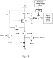
- a specific circuit structure for realizing the crack detection and undesirable-display detection in the display substrate of the present disclosure will be described below with reference to FIG. 3 , in which the connection relationship and operation principle of the related pixel driving circuit of 7T1C, the switching transistor M and the crack detecting wire are mainly described.
- each of the transistors in the pixel driving circuit of 7T1C and the switching transistor M employs a P-type transistor.
- a third transistor T3 is a driving transistor, and a fourth transistor T4 is a scanning transistor.
- a first electrode of a first transistor T1 is coupled to a signal input terminal Vinit
- a second electrode of the first transistor T1 is coupled to a first electrode of a second transistor T2 and a control electrode of a third transistor T3, and a control electrode of the first transistor T1 is coupled to a reset signal terminal Reset.
- the first electrode of the second transistor T2 is coupled to the source of the first transistor T1 and the control electrode of the third transistor T3, a second electrode of the second transistor T2 is coupled to a first electrode of the third transistor T3 and a source of a sixth transistor T6, and a control electrode of the second transistor T2 is coupled to a gate line Gate.
- the first electrode of the third transistor T3 is coupled to the source of the second transistor T2 and the source of the sixth transistor T6, and a second electrode of the third transistor T3 is coupled to a first electrode of the fifth transistor T5 and a first electrode of a fourth transistor T4, and the control electrode of the third transistor T3 is coupled to a first end of the capacitor Cst and the first electrode of the second transistor T2.
- the first electrode of the fourth transistor T4 is coupled to the first electrode of the fifth transistor T5 and the source of the third transistor T3, and a second electrode of the fourth transistor T4 is coupled to the data line Data and in turn coupled to a first electrode of the switching transistor M, a control electrode of the fourth transistor T4 is coupled to the gate line Gate.
- the first electrode of the fifth transistor T5 is coupled to the source of the third transistor T3 and the first electrode of the fourth transistor T4, and a second electrode of the fifth transistor T5 is coupled to a first power supply voltage terminal and a second end of the storage capacitor Cst, a control electrode of the fifth transistor T5 is coupled to a light-emitting control line EM.
- a first electrode of a sixth transistor T6 is coupled to a first electrode of a seventh transistor T7 and a first electrode of a light-emitting device OLED, a second electrode of sixth transistor T6 is coupled to the source of the second transistor T2 and the first electrode of the third transistor T3, an control electrode of sixth transistor T6 is coupled to the light-emitting control line EM.
- the first electrode of the seventh transistor T7 is coupled to the first electrode of the sixth transistor T6 and the first electrode of the light-emitting device OLED, and a second electrode of the seventh transistor T7 is coupled to the signal input terminal Vinit, and a control electrode of the seventh transistor T7 is coupled to a reset signal terminal Reset.
- a second electrode of the light-emitting device OLED is coupled to a second power voltage terminal.
- the first electrode of the switching transistor M is coupled to the data line Data, a second electrode of the switching transistor M is coupled to the data voltage supply circuit, and a control electrode of the switching transistor M is coupled to an end of the crack detecting wire, another end of the crack detecting wire is coupled to a switching voltage supply circuit.
- the scanning transistor (the fourth transistor) T4 is configured to control whether the pixel driving circuit is gated, and the driving transistor (the third transistor) T3 is configured to supply a driving current to the light-emitting device after the switching transistor M is turned on.
- the source of the driving transistor T3 is coupled to the first power supply voltage terminal through the fifth transistor.
- the driving transistor operates in the saturation region due to the first power supply voltage from the first power supply voltage terminal.
- both the driving transistor and the switching transistor M are in the sub-threshold swing (SS) section during the crack detection stage, and a small change in the gate-source voltage may cause a significant influence on the source-drain current, and since the data line Data is coupled to the crack detecting wire through the switching transistor M, a rate of writing the second data voltage to the data line Data is significantly lowered.
- the power supply voltage applied to the gate of the driving transistor is adjusted to increase the gate-source voltage of the driving transistor, therefore it can quickly and accurately determine whether the crack detecting wire is abnormal by detecting the change in the resistance of the crack detecting wire.
- a first data voltage of 7 V output from the data voltage supply circuit is output to the drain of the switching transistor M through the ET signal line and is finally input to the data line Data.
- the gate-source voltage of the switching transistor M ranges from -7V to -13V, and the switching transistor M operates in the linear region.
- fluctuation of the voltage of the gate of the switching transistor M has no significant influence on the output of the source-drain current, the simulation results are shown in Fig. 4 . As can be seen from Fig.
- the currents output to the light emitting device OLED are almost the same, and in the undesirable-display detection stage, no display defect, such as typical horizontal stripes due to breakage of the crack detecting wire, appears on the display panel, therefore, the normal undesirable-display detection cannot be affected, and the effect of shielding the amplifying circuit is achieved.
- the numeral 1 in the drawing represents a current change curve in a case where the resistance of the crack detecting wire is 1 ⁇
- the numeral 2 represents a current change curve in a case where the resistance of the crack detecting wire is 1 M ⁇
- Fig. 5 is similar.
- the second switching voltage written to the gate of the switching transistor M is adjusted to about 2.5V, and the second data voltage written to the second electrode of the switching transistor M is adjusted to about 4V, at this time, the gate-source voltage of the switching transistor M is 1.5V.
- the switching transistor M Since Vgs equals to 1.5V, the switching transistor M operates in the normal PMOS sub-threshold swing (SS) section, and the influence of small change in Vgs on the current is obvious, and since the efficiency of writing the second data voltage is decreased significantly, the first power supply voltage Vdd received by the source of the driving transistor in the pixel circuit is adjusted to 0.1V, the Vgs of the driving transistor is increased, and the driving transistor also operates in the SS section, therefore it can quickly and accurately determine whether the crack detecting wire is abnormal by detecting the change in the resistance of the crack detecting wire. As shown in the simulation results in Fig. 5 , when the resistance of the crack detecting wire changes from 1 ⁇ to 1 M ⁇ , the current output from the light-emitting device OLED changes significantly.
- SS normal PMOS sub-threshold swing
- the output current of the light-emitting device OLED changes more obviously.
- the crack detecting wire is provided in the non-display area Q2, and the crack detecting wire is provided to surround the display area Q1.
- Such an arrangement does not affect the aperture ratio of the display area Q1 of the display substrate, and also does not affect the signal transmission in the display area Q1.
- the crack detecting wire has a length capable of surrounding the display area 2-3 turns.
- the length of the crack detecting wire may be specifically set according to the size of the display substrate.
- the crack detecting wire is provided in a same layer as the gate line Gate in the display substrate, and is made of a same material as the gate line Gate. It should be noted that providing in the same layer may represent that layer structures are located at a same horizontal plane, or have a step difference therebetween. In this way, the crack detecting wire can be formed while forming the gate line Gate in the display substrate, therefore no additional process step is increased and the cost is not increased.
- the material of the crack detecting wire may be a material having a good electrical conductivity, such as molybdenum.
- the display substrate in the present embodiment may be an LCD array substrate in a liquid crystal panel, or may be an OLED array substrate in an OLED display device. In the present embodiment, description is made by taking the display substrate being an OLED array substrate as an example.
- An embodiment of the present disclosure further provides a method for detecting a display substrate, and the display substrate may be the aforementioned display substrate.
- the method for detecting the display substrate includes two stages, that is, an undesirable-display detection stage and a crack detection stage.
- controlling the switching voltage supply circuit to output the first switching voltage to the control electrode of the switching transistor; controlling the data voltage supply circuit to output the first data voltage to the second electrode of the switching transistor, so that the switching transistor operates in a linear region to detect whether or not the display of the display substrate is defective.
- the switching voltage supply circuit outputs the first switching voltage to the control electrode of the switching transistor through the crack detecting wire, and the data voltage supply circuit outputs the first data voltage to the drain of the switching transistor through the data line Data, and the switching transistor operates in a linear region during this stage.
- the switching voltage supply circuit outputs a second switching voltage to the control electrode of the switching transistor through the crack detecting wire, and the data voltage supply circuit outputs the second data voltage to the drain of the switching transistor through the data line Data, and the switching transistor operates in a saturation region during this stage.
- a small change in the voltage of the gate of the switching transistor can cause a large change in the source-drain current of the switching transistor, as long as the crack detecting wire breaks, its resistance changes, the voltage applied to the gate of the switching transistor changes, resulting in a large change in the source-drain current of the switching transistor, that is, the switching transistor operating in the saturation region is equivalent to an amplifying circuit of the crack detecting wire, thus the crack detection may be more accurate.
- the display substrate in the present embodiment further includes a pixel driving circuit.
- the pixel driving circuit may be a pixel driving circuit of 2T1C or a pixel driving circuit of 7T1C.
- the pixel driving circuit may be a pixel driving circuit of other structure.
- the crack detection stage further includes: applying the first power supply voltage, so that the driving transistor operates in the saturation region.
- both the driving transistor and the switching transistor M operate in the sub-threshold swing (SS) section during the crack detection stage, and a small change in the gate-source voltage may cause a significant influence on the source-drain current, and since the data line Data is coupled to the crack detecting wire through the switching transistor M, a rate of writing the second data voltage to the data line Data is significantly lowered.
- the power supply voltage applied to the gate of the driving transistor is adjusted to increase the gate-source voltage of the driving transistor, therefore it can quickly and accurately determine whether the crack detecting wire is abnormal by detecting the change in the resistance of the crack detecting wire.
- a first data voltage of 7 V output from the data voltage supply circuit is output to the drain of the switching transistor M through the ET signal line and is finally input to the data line Data.
- the gate-source voltage of the switching transistor M ranges from -7V to -13V, and the switching transistor M operates in the linear region.
- fluctuation of the voltage of the gate of the switching transistor M has no significant influence on the output of the source-drain current, the simulation results are shown in Fig. 4 . As can be seen from Fig.
- the second switching voltage written to the gate of the switching transistor M is adjusted to about 2.5V, and the second data voltage written to the second electrode of the switching transistor M is adjusted to about 4V, at this time, the gate-source voltage of the switching transistor M is 1.5V.
- the switching transistor M Since Vgs equals to 1.5V, the switching transistor M operates in the normal PMOS sub-threshold swing (SS) section, and the influence of small change in Vgs on the current is obvious, and since the efficiency of writing the second data voltage is decreased significantly, the first power supply voltage Vdd received by the source of the driving transistor in the pixel circuit is adjusted to 0.1V, the Vgs of the driving transistor is increased, so that the driving transistor also operates in the SS section, therefore it can quickly and accurately determine whether the crack detecting wire PCD is abnormal by the change in the resistance of the crack detecting wire is abnormal. As shown in the simulation results in Fig.
- An embodiment of the present disclosure provides a display device including the display substrate in the foregoing embodiments.
- the detection of the display device of the present embodiment is more accurate.
- the display device may be a liquid crystal display device or an light-emitting display device, for example, a product or component having display function, such as a liquid crystal panel, an electronic paper, an OLED panel, a mobile phone, a tablet computer, a television, a display, a notebook computer, a digital photo frame, a navigator, and so on.
- a liquid crystal display device or an light-emitting display device, for example, a product or component having display function, such as a liquid crystal panel, an electronic paper, an OLED panel, a mobile phone, a tablet computer, a television, a display, a notebook computer, a digital photo frame, a navigator, and so on.
- the present disclosure has the following beneficial effects.
- the switching voltage supply circuit When the display substrate in the present embodiment is subjected to the undesirable-display detection, the switching voltage supply circuit outputs the first switching voltage to the control electrode of the switching transistor through the crack detecting wire, and the data voltage supply circuit outputs the first data voltage to the drain of the switching transistor through the data line, and the switching transistor operates in a linear region during this stage. Therefore, changes in the voltage of the gate of the switching transistor would not affect the change of the source-drain current of the switching transistor.
- the switching voltage supply circuit outputs the second switching voltage to the control electrode of the switching transistor through the crack detecting wire
- the data voltage supply circuit outputs the second data voltage to the first electrode of the switching transistor through the data line
- the switching transistor operates in a saturated region during this stage. Therefore, a small change in the voltage of the control electrode of the switching transistor may result in a large change in the source-drain current of the switching transistor.
- the crack detecting wire breaks, the resistance of the crack detecting wire changes, and the voltage applied to the gate of the switching transistor changes, resulting in a large change in the source-drain current of the switching transistor, i.e. the switching transistor operating in the saturation region is equivalent to an amplifying circuit of the crack detecting wire, so that the crack detecting is more accurate.
Landscapes
- Engineering & Computer Science (AREA)
- Physics & Mathematics (AREA)
- General Physics & Mathematics (AREA)
- Computer Hardware Design (AREA)
- Theoretical Computer Science (AREA)
- Crystallography & Structural Chemistry (AREA)
- Chemical & Material Sciences (AREA)
- Nonlinear Science (AREA)
- Microelectronics & Electronic Packaging (AREA)
- Mathematical Physics (AREA)
- Optics & Photonics (AREA)
- Electroluminescent Light Sources (AREA)
- Control Of Indicators Other Than Cathode Ray Tubes (AREA)
- Control Of El Displays (AREA)
Abstract
Description
- The present application claims priority to Chinese Patent Application No.
201810258058.4 filed on March 27, 2018 - The present disclosure relates to the field of display technology, and in particular, to a display substrate, a method for detecting the same, and a display device.
- Currently, most of OLED flexible products adopt a design of crack detecting wire to perform a panel crack detect (PCD). In this design, a metal wire is provided to surround a circumference of display panel several turns and then coupled to data lines in a display area. In a case where the crack detecting wire breaks, a resistance of the crack detecting wire increases, causing insufficient writing of a data voltage on the data line connected thereto. For example, for a conventional pixel driving circuit of 7T1C, insufficiently writing of the data voltage may result in a number of bright lines in the display panel, depending on which a crack in a film layer can be detected.
- An embodiment of the present disclosure provides a display substrate including a display area and a non-display area surrounding the display area, the display substrate further including data lines extending from the display area to the non-display area, wherein the non-display area is provided with at least one switching transistor, a first electrode of each switching transistor is coupled to one of the data lines respectively, a second electrode of each switching transistor is coupled to a data voltage supply circuit, and at least one crack detecting wire, corresponding to the at least one switching transistor in one-to-one correspondence, is provided in the display area, one end of the crack detecting wire is coupled to a control electrode of a corresponding switching transistor, and the other end of the crack detecting wire is coupled to a switching voltage supply circuit.
- In some implementations, in a case where performing a display failure detection, the switching voltage supply circuit is configured to output a first switching voltage, and the data voltage supply circuit is configured to output a first data voltage, so that the switching transistor operates in a linear region.
- In some implementations, in the case where performing a crack detection, the switching voltage supply circuit is configured to output a second switching voltage, and the data voltage supply circuit is configured to output a second data voltage, so that the switching transistor operates in a saturation region.
- In some implementations, a pixel driving circuit is provided in the display area, the pixel driving circuit including a driving transistor, in a case where performing a crack detection, a second electrode of the driving transistor is coupled to a first power supply voltage, so that the driving transistor operates in a saturation region.
- In some implementations, the crack detecting wire is provided to surround the display area.
- In some implementations, the crack detecting wire surrounds the
display area - In some implementations, the display substrate further including a gate line, and the crack detecting wire is provided in a same layer as the gate line, and is made of a same material as the gate line.
- In some implementations, a material of the crack detecting wire includes molybdenum.
- In some implementations, the switching transistor includes a P-type transistor.
- In some implementations, the display substrate including an LCD array substrate or an OLED array substrate.
- An embodiment of the present disclosure provides a method for detecting the above display substrate, including a display fault detection stage and a crack detection stage, wherein
in the display fault detection stage, controlling a switching voltage supply circuit to output a first switching voltage to a control electrode of the switching transistor; and controlling a data voltage supply circuit to output a first data voltage to a second electrode of the switching transistor so that the switching transistor operates in a linear region, so as to detect whether there is a defect in the display of the display substrate;
in the crack detection stage, controlling the switching voltage supply circuit to output a second switching voltage to the control electrode of the switching transistor, and controlling the data voltage supply circuit to output a second data voltage to the second electrode of the switching transistor, so that the switching transistor operates in a saturation region, so as to detect whether there is a crack in the crack detecting wire. - In some implementations, the display area is provided with a pixel driving circuit, and the pixel driving circuit includes a driving transistor, and the crack detection stage further includes:
supplying a first power supply voltage to the second electrode of the driving transistor, so that the driving transistor operates in the saturation region. - An embodiment of the present disclosure provides a display device including the above display substrate.
-
-
Fig. 1 is a structural diagram of a display substrate according to an embodiment of the present disclosure; -
Fig. 2 is a circuit diagram of a display substrate according to an embodiment of the present disclosure; -
Fig. 3 is a schematic diagram of an Id-Vg curve of a P-type transistor; -
Fig. 4 shows an influence of changes in a resistance of a crack detecting wire on a current of a light emitting device in an undesirable-display detection stage, according to an embodiment of the present disclosure; -
Fig. 5 shows an influence of changes in a resistance of a crack detection wire on a current of a light emitting device in a crack detection stage, according to an embodiment of the present disclosure. - To enable those skilled in the art to better understand the technical solutions of the present disclosure, the present disclosure will be further described in detail below in conjunction with the drawings and specific embodiments.
- With the continuous improvement of product resolution (PPI: pixels per inch) and the popularity of full-screen, a space for arranging a detection switch in the display panel is becoming narrower and narrower. Currently, the single-sided switch is frequently used to perform Cell Test (that is, undesirable-display detection) on a display panel. For the PCD, there are no more switches available for controlling the PCD, resulting in that the PCD cannot be turned off during the Cell Test of the display product. Due to the resistance of the crack detecting wire for the PCD, the data voltage signal coupled to the crack detecting wire has a significant voltage drop, the writing of the data voltage is insufficient, and a bright line or a dark line may appear in different circuits, which causes the Cell Test process being affected by a vertical line PCD-X-Line, the normal undesirable-product detection is affected and excessive test and misjudgment may occur, affecting product quality and yield.
- As described in
Fig. 1 , an embodiment of the present disclosure provides a display substrate including a display area Q1 and a non-display area Q2 surrounding the display area Q1. The display substrate further includes: a data line Data extending from the display area Q1 to the non-display area Q2; a switching transistor and a crack detecting line provided in the non-display area Q2; wherein an end of the crack detecting wire is coupled to a control electrode of the switching transistor, and another end of the crack detecting wire is coupled to a switching voltage supply circuit; a first electrode of the switching transistor is coupled to the data line Data, and a second electrode of the switching transistor is coupled to a data voltage supply circuit. In an undesirable-display detection stage, the switching voltage supply circuit is configured to output a first switching voltage, the data voltage supply circuit is configured to output a first data voltage, and the switching transistor operates in a linear region; and in a crack detection stage, the switching voltage supply circuit is configured to output a second switching voltage, the data voltage supply circuit is configured to output a second data voltage, and the switching transistor operates in a saturation region. - In the present embodiment, the description will be made by taking each of the transistors in the display substrate being a P-type transistor as an example, and the first electrode of the transistor is a drain, the second electrode of the transistor is a source, and the control electrode of the transistor is a gate. The linear region of the switching transistor in the present embodiment is located near Ion of the Id-Vg characteristic curve of the switching transistor, and the saturation region of the switching transistor is located near the sub-threshold value of the Id-Vg characteristic curve of the switching transistor.
- In the present embodiment, in a case where the display substrate is subjected to the undesirable-display detection, the switching voltage supply circuit outputs the first switching voltage to the control electrode of the switching transistor through the crack detecting wire, and the data voltage supply circuit outputs the first data voltage to the drain of the switching transistor, and the switching transistor operates in a linear region during this stage. Therefore, changes in voltage of the gate of the switching transistor would not affect a change in source-drain current of the switching transistor, that is, even if the crack detecting wire breaks during the undesirable-display detection stage, the resistance of the crack detecting wire changes from 1 Ω to 1 MΩ, and a change in voltage of the control electrode of the switching transistor occurs, the current output from the drain of the switching transistor to the data line Data cannot be affected, that is, the undesirable-display detection of the display substrate cannot be affected. It can be seen that the switching transistor being controlled to operate in the linear region is equivalent to shielding the crack detecting wire. Correspondingly, when the display substrate of the present embodiment is subjected to the crack detection, the switching voltage supply circuit outputs a second switching voltage to the control electrode of the switching transistor through the crack detecting wire, and the data voltage supply circuit outputs the second data voltage to the drain of the switching transistor, and the switching transistor operates in a saturation region during this stage. Therefore, a small change in the voltage of the gate of the switching transistor can cause a large change in the source-drain current of the switching transistor, thus, as long as the crack detecting wire breaks, its resistance changes, the voltage applied to the gate of the switching transistor changes, resulting in a large change in the source-drain current of the switching transistor, that is, the switching transistor operating in the saturation region is equivalent to an amplifying circuit of the crack detecting wire, so that the crack detection may be more accurate.
- The display area Q1 of the display substrate of the present embodiment is provided with a pixel driving circuit therein, and the pixel driving circuit may be a pixel driving circuit of 2T1C, that is, the pixel driving circuit includes two transistors and one storage capacitor Cst; or the pixel driving circuit may be a pixel driving circuit of 7T1C, that is, the pixel driving circuit includes seven transistors and a storage capacitor Cst. A specific circuit structure for realizing the crack detection and undesirable-display detection in the display substrate of the present disclosure will be described below with reference to
FIG. 3 , in which the connection relationship and operation principle of the related pixel driving circuit of 7T1C, the switching transistor M and the crack detecting wire are mainly described. - As shown in
FIG. 3 , each of the transistors in the pixel driving circuit of 7T1C and the switching transistor M employs a P-type transistor. A third transistor T3 is a driving transistor, and a fourth transistor T4 is a scanning transistor. - Specifically, a first electrode of a first transistor T1 is coupled to a signal input terminal Vinit, a second electrode of the first transistor T1 is coupled to a first electrode of a second transistor T2 and a control electrode of a third transistor T3, and a control electrode of the first transistor T1 is coupled to a reset signal terminal Reset. The first electrode of the second transistor T2 is coupled to the source of the first transistor T1 and the control electrode of the third transistor T3, a second electrode of the second transistor T2 is coupled to a first electrode of the third transistor T3 and a source of a sixth transistor T6, and a control electrode of the second transistor T2 is coupled to a gate line Gate. The first electrode of the third transistor T3 is coupled to the source of the second transistor T2 and the source of the sixth transistor T6, and a second electrode of the third transistor T3 is coupled to a first electrode of the fifth transistor T5 and a first electrode of a fourth transistor T4, and the control electrode of the third transistor T3 is coupled to a first end of the capacitor Cst and the first electrode of the second transistor T2. The first electrode of the fourth transistor T4 is coupled to the first electrode of the fifth transistor T5 and the source of the third transistor T3, and a second electrode of the fourth transistor T4 is coupled to the data line Data and in turn coupled to a first electrode of the switching transistor M, a control electrode of the fourth transistor T4 is coupled to the gate line Gate. The first electrode of the fifth transistor T5 is coupled to the source of the third transistor T3 and the first electrode of the fourth transistor T4, and a second electrode of the fifth transistor T5 is coupled to a first power supply voltage terminal and a second end of the storage capacitor Cst, a control electrode of the fifth transistor T5 is coupled to a light-emitting control line EM. A first electrode of a sixth transistor T6 is coupled to a first electrode of a seventh transistor T7 and a first electrode of a light-emitting device OLED, a second electrode of sixth transistor T6 is coupled to the source of the second transistor T2 and the first electrode of the third transistor T3, an control electrode of sixth transistor T6 is coupled to the light-emitting control line EM. The first electrode of the seventh transistor T7 is coupled to the first electrode of the sixth transistor T6 and the first electrode of the light-emitting device OLED, and a second electrode of the seventh transistor T7 is coupled to the signal input terminal Vinit, and a control electrode of the seventh transistor T7 is coupled to a reset signal terminal Reset. A second electrode of the light-emitting device OLED is coupled to a second power voltage terminal. The first electrode of the switching transistor M is coupled to the data line Data, a second electrode of the switching transistor M is coupled to the data voltage supply circuit, and a control electrode of the switching transistor M is coupled to an end of the crack detecting wire, another end of the crack detecting wire is coupled to a switching voltage supply circuit.
- In the present embodiment, the scanning transistor (the fourth transistor) T4 is configured to control whether the pixel driving circuit is gated, and the driving transistor (the third transistor) T3 is configured to supply a driving current to the light-emitting device after the switching transistor M is turned on. As described above, the source of the driving transistor T3 is coupled to the first power supply voltage terminal through the fifth transistor. In the embodiment, in the crack detection stage, the driving transistor operates in the saturation region due to the first power supply voltage from the first power supply voltage terminal. In this way, both the driving transistor and the switching transistor M are in the sub-threshold swing (SS) section during the crack detection stage, and a small change in the gate-source voltage may cause a significant influence on the source-drain current, and since the data line Data is coupled to the crack detecting wire through the switching transistor M, a rate of writing the second data voltage to the data line Data is significantly lowered. At this time, the power supply voltage applied to the gate of the driving transistor is adjusted to increase the gate-source voltage of the driving transistor, therefore it can quickly and accurately determine whether the crack detecting wire is abnormal by detecting the change in the resistance of the crack detecting wire.
- Specifically, description will be made by taking the switching transistor M adopting a P-type transistor and detecting whether a green pixel displays normally in the undesirable-display detection stage as an example. A first data voltage of 7 V output from the data voltage supply circuit is output to the drain of the switching transistor M through the ET signal line and is finally input to the data line Data. At this time, the gate-source voltage of the switching transistor M ranges from -7V to -13V, and the switching transistor M operates in the linear region. In this case, fluctuation of the voltage of the gate of the switching transistor M has no significant influence on the output of the source-drain current, the simulation results are shown in
Fig. 4 . As can be seen fromFig. 4 , when the resistance of the crack detecting wire is 1Ω or 1 MΩ, the currents output to the light emitting device OLED are almost the same, and in the undesirable-display detection stage, no display defect, such as typical horizontal stripes due to breakage of the crack detecting wire, appears on the display panel, therefore, the normal undesirable-display detection cannot be affected, and the effect of shielding the amplifying circuit is achieved. Thenumeral 1 in the drawing represents a current change curve in a case where the resistance of the crack detecting wire is 1 Ω, and thenumeral 2 represents a current change curve in a case where the resistance of the crack detecting wire is 1 MΩ, andFig. 5 is similar. - In the crack detection stage, the second switching voltage written to the gate of the switching transistor M is adjusted to about 2.5V, and the second data voltage written to the second electrode of the switching transistor M is adjusted to about 4V, at this time, the gate-source voltage of the switching transistor M is 1.5V. Since Vgs equals to 1.5V, the switching transistor M operates in the normal PMOS sub-threshold swing (SS) section, and the influence of small change in Vgs on the current is obvious, and since the efficiency of writing the second data voltage is decreased significantly, the first power supply voltage Vdd received by the source of the driving transistor in the pixel circuit is adjusted to 0.1V, the Vgs of the driving transistor is increased, and the driving transistor also operates in the SS section, therefore it can quickly and accurately determine whether the crack detecting wire is abnormal by detecting the change in the resistance of the crack detecting wire. As shown in the simulation results in
Fig. 5 , when the resistance of the crack detecting wire changes from 1 Ω to 1 MΩ, the current output from the light-emitting device OLED changes significantly. As the change of the resistance of the crack detecting wire intensifies, the output current of the light-emitting device OLED changes more obviously. By adjusting amplitude of the Vdd, adjusting the operation region of the driving transistor, and adjusting the sensitivity to the change in the resistance of the crack detecting wire, it is possible to effectively determine whether the crack detecting wire is broken. - In the present embodiment, the crack detecting wire is provided in the non-display area Q2, and the crack detecting wire is provided to surround the display area Q1. Such an arrangement does not affect the aperture ratio of the display area Q1 of the display substrate, and also does not affect the signal transmission in the display area Q1.
- In some embodiments, the crack detecting wire has a length capable of surrounding the display area 2-3 turns. Certainly, the length of the crack detecting wire may be specifically set according to the size of the display substrate. The crack detecting wire is provided in a same layer as the gate line Gate in the display substrate, and is made of a same material as the gate line Gate. It should be noted that providing in the same layer may represent that layer structures are located at a same horizontal plane, or have a step difference therebetween. In this way, the crack detecting wire can be formed while forming the gate line Gate in the display substrate, therefore no additional process step is increased and the cost is not increased. Specifically, the material of the crack detecting wire may be a material having a good electrical conductivity, such as molybdenum.
- It should be understood that the present disclosure has been described by taking one switching transistor, one crack detecting wire, one data line, one switching voltage supply circuit, and one data voltage supply circuit as an example with reference to the accompanying drawings, but this is merely exemplary, but not limited. A person skilled in the art may provide a plurality of switching transistors, a plurality of data lines, and a plurality of crack detecting wires according to actual applications, wherein the plurality of switching transistors are coupled to the plurality of crack detecting wires respectively in one-to-one correspondence, and at this time, one switching voltage supply circuit and one data voltage supply circuit may be respectively coupled to the plurality of switching transistors. Furthermore, depending on actual applications, a plurality of switching voltage supply circuits and a plurality of data voltage supply circuits may be provided such that each kind of them are coupled to the switching transistors respectively in a one-to-one correspondence.
- The display substrate in the present embodiment may be an LCD array substrate in a liquid crystal panel, or may be an OLED array substrate in an OLED display device. In the present embodiment, description is made by taking the display substrate being an OLED array substrate as an example.
- An embodiment of the present disclosure further provides a method for detecting a display substrate, and the display substrate may be the aforementioned display substrate. The method for detecting the display substrate includes two stages, that is, an undesirable-display detection stage and a crack detection stage.
- In the undesirable-display detection stage, controlling the switching voltage supply circuit to output the first switching voltage to the control electrode of the switching transistor; controlling the data voltage supply circuit to output the first data voltage to the second electrode of the switching transistor, so that the switching transistor operates in a linear region to detect whether or not the display of the display substrate is defective.
- In the crack detection stage, controlling the switching voltage supply circuit to output the second switching voltage to the control electrode of the switching transistor; controlling the data voltage supply circuit to output the second data voltage to the second electrode of the switching transistor so that the switching transistor operates in the saturation region to detect whether there is a crack in the crack detecting wire.
- In the present embodiment, in a case where the display substrate is subjected to the undesirable-display detection, the switching voltage supply circuit outputs the first switching voltage to the control electrode of the switching transistor through the crack detecting wire, and the data voltage supply circuit outputs the first data voltage to the drain of the switching transistor through the data line Data, and the switching transistor operates in a linear region during this stage. Therefore, changes in the voltage of the gate of the switching transistor does not affect the change in the source-drain current of the switching transistor, that is, even if the crack detecting wire breaks during the undesirable-display detection stage, the resistance of the crack detecting wire changes from 1 Ω to 1 MΩ, resulting in a change in the voltage of the control electrode of the switching transistor, the current output from the drain of the switching transistor to the data line Data cannot be affected, that is, the undesirable-display detection of the display substrate cannot be affected. It can be seen that the switching transistor is controlled to operate in the linear region, which is equivalent to shielding the crack detecting wire. Correspondingly, in a case where the display substrate of the present embodiment is subjected to the crack detection, the switching voltage supply circuit outputs a second switching voltage to the control electrode of the switching transistor through the crack detecting wire, and the data voltage supply circuit outputs the second data voltage to the drain of the switching transistor through the data line Data, and the switching transistor operates in a saturation region during this stage. Therefore, a small change in the voltage of the gate of the switching transistor can cause a large change in the source-drain current of the switching transistor, as long as the crack detecting wire breaks, its resistance changes, the voltage applied to the gate of the switching transistor changes, resulting in a large change in the source-drain current of the switching transistor, that is, the switching transistor operating in the saturation region is equivalent to an amplifying circuit of the crack detecting wire, thus the crack detection may be more accurate.
- The display substrate in the present embodiment further includes a pixel driving circuit. The pixel driving circuit may be a pixel driving circuit of 2T1C or a pixel driving circuit of 7T1C. Certainly, the pixel driving circuit may be a pixel driving circuit of other structure. In some embodiments, the crack detection stage further includes: applying the first power supply voltage, so that the driving transistor operates in the saturation region. In this way, both the driving transistor and the switching transistor M operate in the sub-threshold swing (SS) section during the crack detection stage, and a small change in the gate-source voltage may cause a significant influence on the source-drain current, and since the data line Data is coupled to the crack detecting wire through the switching transistor M, a rate of writing the second data voltage to the data line Data is significantly lowered. At this time, the power supply voltage applied to the gate of the driving transistor is adjusted to increase the gate-source voltage of the driving transistor, therefore it can quickly and accurately determine whether the crack detecting wire is abnormal by detecting the change in the resistance of the crack detecting wire.
- Specifically, description will be made by taking the switching transistor M adopting a P-type transistor and detecting whether a green pixel displays normally in the undesirable-display detection stage as an example. A first data voltage of 7 V output from the data voltage supply circuit is output to the drain of the switching transistor M through the ET signal line and is finally input to the data line Data. At this time, the gate-source voltage of the switching transistor M ranges from -7V to -13V, and the switching transistor M operates in the linear region. In this case, fluctuation of the voltage of the gate of the switching transistor M has no significant influence on the output of the source-drain current, the simulation results are shown in
Fig. 4 . As can be seen fromFig. 4 , when the resistance of the crack detecting wire is 1 Ω and 1 MΩ, the currents output to the light emitting device OLED are almost the same, and in the undesirable-display detection stage, no display defect, such as typical horizontal stripes due to breakage of the crack detecting wire, appears on the display panel, therefore, the normal undesirable-display detection cannot be affected, and the effect of shielding the amplifying circuit is achieved. - In the crack detection stage, the second switching voltage written to the gate of the switching transistor M is adjusted to about 2.5V, and the second data voltage written to the second electrode of the switching transistor M is adjusted to about 4V, at this time, the gate-source voltage of the switching transistor M is 1.5V. Since Vgs equals to 1.5V, the switching transistor M operates in the normal PMOS sub-threshold swing (SS) section, and the influence of small change in Vgs on the current is obvious, and since the efficiency of writing the second data voltage is decreased significantly, the first power supply voltage Vdd received by the source of the driving transistor in the pixel circuit is adjusted to 0.1V, the Vgs of the driving transistor is increased, so that the driving transistor also operates in the SS section, therefore it can quickly and accurately determine whether the crack detecting wire PCD is abnormal by the change in the resistance of the crack detecting wire is abnormal. As shown in the simulation results in
Fig. 5 , when the resistance of the crack detecting wire changes from 1 Ω to 1 MΩ, the current output from the light-emitting device OLED changes significantly. As the change of the resistance of the crack detecting wire intensifies, the output current of the light-emitting device OLED changes more obviously. By adjusting amplitude of the Vdd, adjusting the operation region of the driving transistor, so as to adjust the sensitivity to the change in the resistance of the crack detecting wire, it is possible to effectively determine whether the crack detecting wire is broken. - An embodiment of the present disclosure provides a display device including the display substrate in the foregoing embodiments.
- Therefore, the detection of the display device of the present embodiment is more accurate.
- The display device may be a liquid crystal display device or an light-emitting display device, for example, a product or component having display function, such as a liquid crystal panel, an electronic paper, an OLED panel, a mobile phone, a tablet computer, a television, a display, a notebook computer, a digital photo frame, a navigator, and so on.
- The present disclosure has the following beneficial effects.
- When the display substrate in the present embodiment is subjected to the undesirable-display detection, the switching voltage supply circuit outputs the first switching voltage to the control electrode of the switching transistor through the crack detecting wire, and the data voltage supply circuit outputs the first data voltage to the drain of the switching transistor through the data line, and the switching transistor operates in a linear region during this stage. Therefore, changes in the voltage of the gate of the switching transistor would not affect the change of the source-drain current of the switching transistor. Correspondingly, when the display substrate of the present disclosure is subjected to the crack detection, the switching voltage supply circuit outputs the second switching voltage to the control electrode of the switching transistor through the crack detecting wire, and the data voltage supply circuit outputs the second data voltage to the first electrode of the switching transistor through the data line, and the switching transistor operates in a saturated region during this stage. Therefore, a small change in the voltage of the control electrode of the switching transistor may result in a large change in the source-drain current of the switching transistor. In this way, if the crack detecting wire breaks, the resistance of the crack detecting wire changes, and the voltage applied to the gate of the switching transistor changes, resulting in a large change in the source-drain current of the switching transistor, i.e. the switching transistor operating in the saturation region is equivalent to an amplifying circuit of the crack detecting wire, so that the crack detecting is more accurate.
- It should be understood that, the foregoing embodiments are only exemplary embodiments used for explaining the principle of the present disclosure, but the present disclosure is not limited thereto. Various variations and modifications may be made by a person skilled in the art without departing from the spirit and essence of the present disclosure, and these variations and modifications also fall into the protection scope of the present disclosure.
Claims (13)
- A display substrate, comprising a display area and a non-display area surrounding the display area, the display substrate further comprising data lines extending from the display area to the non-display area, wherein the non-display area is provided with at least one switching transistor, a first electrode of each switching transistor is coupled to one of the data lines, a second electrode of each switching transistor is coupled to a data voltage supply circuit, and at least one crack detecting wire, corresponding to the at least one switching transistor in one-to-one correspondence, is provided in the display area, an end of the crack detecting wire is coupled to a control electrode of the switching transistor corresponding to the crack detecting wire, and another end of the crack detecting wire is coupled to a switching voltage supply circuit.
- The display substrate according to claim 1, wherein in a case where performing an undesirable-display detection, the switching voltage supply circuit is configured to output a first switching voltage, and the data voltage supply circuit is configured to output a first data voltage, and the switching transistor operates in a linear region.
- The display substrate according to claim 1, wherein, in a case where performing a crack detection, the switching voltage supply circuit is configured to output a second switching voltage, and the data voltage supply circuit is configured to output a second data voltage, and the switching transistor operates in a saturation region.
- The display substrate according to claim 3, wherein a pixel driving circuit is provided in the display area, the pixel driving circuit comprising a driving transistor, in a case where performing the crack detection, a second electrode of the driving transistor is coupled to a first power supply voltage, and the driving transistor operates in a saturation region.
- The display substrate according to claim 1, wherein the crack detecting wire is provided to surround the display area.
- The display substrate according to claim 5, wherein the crack detecting wire surrounds the display area 2 or 3 turns.
- The display substrate according to claim 1, wherein the display substrate further comprising a gate line, and the crack detecting wire is provided in a same layer as the gate line, and is made of a same material as the gate line.
- The display substrate according to claim 1, wherein a material of the crack detecting wire comprises molybdenum.
- The display substrate according to any one of claims 1 to 3, wherein the switching transistor comprises a P-type transistor.
- The display substrate according to claim 1, wherein the display substrate comprising an LCD array substrate or an OLED array substrate.
- A method for detecting a display substrate according to any one of claims 1 to 10, comprising an undesirable-display detection stage and a crack detection stage, wherein
in the undesirable-display detection stage, controlling a switching voltage supply circuit to output a first switching voltage to a control electrode of the switching transistor; and controlling a data voltage supply circuit to output a first data voltage to a second electrode of the switching transistor so that the switching transistor operates in a linear region, so as to detect whether there is a defect in the display of the display substrate;
in the crack detection stage, controlling the switching voltage supply circuit to output a second switching voltage to the control electrode of the switching transistor, and controlling the data voltage supply circuit to output a second data voltage to the second electrode of the switching transistor, so that the switching transistor operates in a saturation region, so as to detect whether there is a crack in the crack detecting wire. - The method according to claim 11, wherein the display area is provided with a pixel driving circuit therein, and the pixel driving circuit comprises a driving transistor, and the crack detection stage further comprises:
supplying a first power supply voltage to the second electrode of the driving transistor, so that the driving transistor operates in the saturation region. - A display device, comprising the display substrate according to any one of claims 1 to 10.
Applications Claiming Priority (2)
| Application Number | Priority Date | Filing Date | Title |
|---|---|---|---|
| CN201810258058.4A CN110211517B (en) | 2018-03-27 | 2018-03-27 | Display substrate, detection method thereof and display device |
| PCT/CN2018/114586 WO2019184371A1 (en) | 2018-03-27 | 2018-11-08 | Display substrate and detection method thereof, and display device |
Publications (2)
| Publication Number | Publication Date |
|---|---|
| EP3779942A1 true EP3779942A1 (en) | 2021-02-17 |
| EP3779942A4 EP3779942A4 (en) | 2022-01-05 |
Family
ID=67779066
Family Applications (1)
| Application Number | Title | Priority Date | Filing Date |
|---|---|---|---|
| EP18857435.4A Pending EP3779942A4 (en) | 2018-03-27 | 2018-11-08 | DISPLAY SUBSTRATE AND ITS DETECTION METHOD AND DISPLAY DEVICE |
Country Status (4)
| Country | Link |
|---|---|
| US (1) | US11361690B2 (en) |
| EP (1) | EP3779942A4 (en) |
| CN (1) | CN110211517B (en) |
| WO (1) | WO2019184371A1 (en) |
Families Citing this family (10)
| Publication number | Priority date | Publication date | Assignee | Title |
|---|---|---|---|---|
| CN111223408B (en) * | 2020-02-11 | 2022-03-25 | 京东方科技集团股份有限公司 | Display panel, edge damage detection method, preparation method and display device |
| CN111354296B (en) * | 2020-04-16 | 2023-01-24 | 京东方科技集团股份有限公司 | display panel, display device |
| CN111696459B (en) * | 2020-05-26 | 2023-10-20 | 京东方科技集团股份有限公司 | Detection module, crack detection method, display panel and display device |
| CN112289837A (en) * | 2020-10-27 | 2021-01-29 | 昆山国显光电有限公司 | Display substrate, detection method thereof and display device |
| CN112419949B (en) * | 2020-12-15 | 2022-04-05 | 武汉华星光电半导体显示技术有限公司 | Display panel and display device |
| CN113473826B (en) * | 2021-06-09 | 2022-07-05 | 荣耀终端有限公司 | Glass substrate, display panel, display and electronic equipment |
| JP7775009B2 (en) * | 2021-10-04 | 2025-11-25 | 上海天馬微電子有限公司 | Liquid crystal display device and line defect detection method |
| KR20230102047A (en) * | 2021-12-29 | 2023-07-07 | 삼성디스플레이 주식회사 | Display device |
| CN114550628B (en) * | 2022-02-24 | 2025-07-25 | 京东方科技集团股份有限公司 | Display panel, display device and crack detection method of display panel |
| CN118298761B (en) * | 2024-05-11 | 2026-01-20 | 京东方科技集团股份有限公司 | Pixel circuit, detection method and display device |
Family Cites Families (19)
| Publication number | Priority date | Publication date | Assignee | Title |
|---|---|---|---|---|
| KR101365673B1 (en) | 2006-11-24 | 2014-02-21 | 삼성디스플레이 주식회사 | Thin film transistor, thin film transistor substrate including the same and menufacturing method thereof |
| KR20140015887A (en) * | 2012-07-26 | 2014-02-07 | 삼성디스플레이 주식회사 | Safety driving system of display device and safety driving method of display device |
| JP6138480B2 (en) * | 2012-12-20 | 2017-05-31 | 株式会社ジャパンディスプレイ | Display device |
| JP6562608B2 (en) * | 2013-09-19 | 2019-08-21 | 株式会社半導体エネルギー研究所 | Electronic device and driving method of electronic device |
| US9983452B2 (en) * | 2014-07-15 | 2018-05-29 | Huawei Technologies Co., Ltd. | Method for detecting substrate crack, substrate, and detection circuit |
| CN204116461U (en) * | 2014-07-31 | 2015-01-21 | 上海天马微电子有限公司 | Display panel |
| KR102246365B1 (en) * | 2014-08-06 | 2021-04-30 | 삼성디스플레이 주식회사 | Display device and fabricating method of the same |
| CN104407481B (en) * | 2014-12-09 | 2017-05-10 | 京东方科技集团股份有限公司 | Array substrate, detection method of failure of signal line, display panel and display device |
| CN104535620B (en) * | 2015-01-16 | 2017-05-24 | 友达光电(厦门)有限公司 | Display panel and crack detection method thereof |
| KR102409454B1 (en) * | 2015-02-02 | 2022-06-15 | 삼성디스플레이 주식회사 | Display panel |
| KR102417143B1 (en) * | 2015-04-29 | 2022-07-05 | 삼성디스플레이 주식회사 | Display device |
| KR102343803B1 (en) * | 2015-06-16 | 2021-12-29 | 삼성디스플레이 주식회사 | Display Apparatus and Inspecting Method Thereof |
| CN105976744B (en) * | 2016-06-24 | 2023-03-31 | 山东影响力智能科技有限公司 | Screen module, electronic equipment and micro-crack detection method of screen module |
| KR102561277B1 (en) * | 2016-08-01 | 2023-07-28 | 삼성디스플레이 주식회사 | Display device |
| KR102769951B1 (en) * | 2016-08-22 | 2025-02-18 | 삼성디스플레이 주식회사 | Display device |
| KR102351323B1 (en) * | 2017-03-28 | 2022-01-17 | 삼성전자주식회사 | Circuit for sensing crack of display and electronic device including the same |
| US10605855B2 (en) * | 2017-08-29 | 2020-03-31 | Taiwan Semiconductor Manufacturing Co., Ltd. | Method, test line and system for detecting semiconductor wafer defects |
| CN111667784B (en) * | 2020-06-09 | 2023-03-31 | 昆山国显光电有限公司 | Display panel, driving method of display panel and display device |
| CN112289837A (en) * | 2020-10-27 | 2021-01-29 | 昆山国显光电有限公司 | Display substrate, detection method thereof and display device |
-
2018
- 2018-03-27 CN CN201810258058.4A patent/CN110211517B/en active Active
- 2018-11-08 US US16/338,332 patent/US11361690B2/en active Active
- 2018-11-08 EP EP18857435.4A patent/EP3779942A4/en active Pending
- 2018-11-08 WO PCT/CN2018/114586 patent/WO2019184371A1/en not_active Ceased
Also Published As
| Publication number | Publication date |
|---|---|
| EP3779942A4 (en) | 2022-01-05 |
| US11361690B2 (en) | 2022-06-14 |
| CN110211517B (en) | 2021-03-16 |
| CN110211517A (en) | 2019-09-06 |
| WO2019184371A1 (en) | 2019-10-03 |
| US20210366325A1 (en) | 2021-11-25 |
Similar Documents
| Publication | Publication Date | Title |
|---|---|---|
| US11361690B2 (en) | Display substrate and method for detecting the same, and display device | |
| CN108510940B (en) | Display screen, and display screen brightness compensation method and compensation device | |
| EP3163559B1 (en) | Pixel circuit, display panel and display device | |
| US10439610B2 (en) | Force touch detection circuit, method and display panel | |
| US11238767B2 (en) | Array substrate, display device and method for detecting the same | |
| KR20200003023A (en) | Display panel and its crack detection method, display device | |
| US10672675B2 (en) | Circuit and method for testing gate lines of array substrate | |
| US10102783B2 (en) | Array substrate and detecting method for an array substrate | |
| US20160266689A1 (en) | Pixel circuit, display panel and display apparatus | |
| CN105632383B (en) | A kind of test circuit, test method, display panel and display device | |
| CN112331141A (en) | OLED display panel and display device | |
| US20180067582A1 (en) | In-cell touch panel and display device | |
| CN103413524A (en) | Organic light-emitting diode pixel circuit, method for driving same and display device | |
| US10916193B2 (en) | Pixel driving circuit, display device, and driving method | |
| WO2020228411A1 (en) | Display substrate, driving method therefor, and display device | |
| US10763391B2 (en) | Display panel, method for processing defective pixels thereof, display device | |
| CN110853558B (en) | Flexible display screen, detection method thereof and display device | |
| JP7195928B2 (en) | Charge emission circuit, display substrate, display device and charge emission method thereof | |
| CN107705737B (en) | Method and device for detecting poor short circuit | |
| CN113394258A (en) | Display panel and display device | |
| CN108597424B (en) | Display panel, display device and detection method | |
| CN113466252A (en) | Display panel, detection method of display panel and display device | |
| CN108169972A (en) | Array substrate and its driving method, display device | |
| JP2006208137A (en) | Matrix structure defect detection method and matrix structure defect detection apparatus | |
| CN118588022B (en) | Display screen, crack detection method and display |
Legal Events
| Date | Code | Title | Description |
|---|---|---|---|
| STAA | Information on the status of an ep patent application or granted ep patent |
Free format text: STATUS: UNKNOWN |
|
| STAA | Information on the status of an ep patent application or granted ep patent |
Free format text: STATUS: THE INTERNATIONAL PUBLICATION HAS BEEN MADE |
|
| PUAI | Public reference made under article 153(3) epc to a published international application that has entered the european phase |
Free format text: ORIGINAL CODE: 0009012 |
|
| STAA | Information on the status of an ep patent application or granted ep patent |
Free format text: STATUS: REQUEST FOR EXAMINATION WAS MADE |
|
| 17P | Request for examination filed |
Effective date: 20190329 |
|
| AK | Designated contracting states |
Kind code of ref document: A1 Designated state(s): AL AT BE BG CH CY CZ DE DK EE ES FI FR GB GR HR HU IE IS IT LI LT LU LV MC MK MT NL NO PL PT RO RS SE SI SK SM TR |
|
| AX | Request for extension of the european patent |
Extension state: BA ME |
|
| DAV | Request for validation of the european patent (deleted) | ||
| DAX | Request for extension of the european patent (deleted) | ||
| A4 | Supplementary search report drawn up and despatched |
Effective date: 20211207 |
|
| RIC1 | Information provided on ipc code assigned before grant |
Ipc: G09G 3/3291 20160101ALN20211201BHEP Ipc: G09G 3/3233 20160101ALI20211201BHEP Ipc: G09G 3/00 20060101AFI20211201BHEP |
|
| STAA | Information on the status of an ep patent application or granted ep patent |
Free format text: STATUS: EXAMINATION IS IN PROGRESS |
|
| 17Q | First examination report despatched |
Effective date: 20241023 |