EP3779522A1 - Verarbeitungstechnologie für einspaltige und mehrreihige äquivalente feldlinse mit negativem brechungsindex - Google Patents
Verarbeitungstechnologie für einspaltige und mehrreihige äquivalente feldlinse mit negativem brechungsindex Download PDFInfo
- Publication number
- EP3779522A1 EP3779522A1 EP18925489.9A EP18925489A EP3779522A1 EP 3779522 A1 EP3779522 A1 EP 3779522A1 EP 18925489 A EP18925489 A EP 18925489A EP 3779522 A1 EP3779522 A1 EP 3779522A1
- Authority
- EP
- European Patent Office
- Prior art keywords
- strip
- shaped optical
- optical waveguide
- waveguide array
- plates
- Prior art date
- Legal status (The legal status is an assumption and is not a legal conclusion. Google has not performed a legal analysis and makes no representation as to the accuracy of the status listed.)
- Pending
Links
- 238000005516 engineering process Methods 0.000 title description 9
- 230000003287 optical effect Effects 0.000 claims abstract description 100
- 239000000463 material Substances 0.000 claims abstract description 21
- 239000003292 glue Substances 0.000 claims abstract description 15
- 238000005520 cutting process Methods 0.000 claims abstract description 10
- 238000003672 processing method Methods 0.000 claims abstract description 9
- 238000004026 adhesive bonding Methods 0.000 claims abstract description 8
- XAGFODPZIPBFFR-UHFFFAOYSA-N aluminium Chemical compound [Al] XAGFODPZIPBFFR-UHFFFAOYSA-N 0.000 claims abstract description 8
- 229910052782 aluminium Inorganic materials 0.000 claims abstract description 8
- 230000001681 protective effect Effects 0.000 claims abstract description 5
- 238000007747 plating Methods 0.000 claims abstract description 4
- 238000010438 heat treatment Methods 0.000 claims abstract description 3
- 238000003825 pressing Methods 0.000 claims abstract description 3
- 238000002791 soaking Methods 0.000 claims abstract description 3
- 238000003384 imaging method Methods 0.000 abstract description 45
- 238000010586 diagram Methods 0.000 description 7
- 239000010408 film Substances 0.000 description 6
- 230000000694 effects Effects 0.000 description 5
- 239000011521 glass Substances 0.000 description 5
- 239000011241 protective layer Substances 0.000 description 5
- 230000004075 alteration Effects 0.000 description 4
- 238000003491 array Methods 0.000 description 3
- 239000000084 colloidal system Substances 0.000 description 3
- 230000007547 defect Effects 0.000 description 3
- 239000012535 impurity Substances 0.000 description 3
- 238000004519 manufacturing process Methods 0.000 description 3
- 238000000034 method Methods 0.000 description 3
- 239000002994 raw material Substances 0.000 description 2
- 239000002699 waste material Substances 0.000 description 2
- 206010010071 Coma Diseases 0.000 description 1
- 238000004458 analytical method Methods 0.000 description 1
- 201000009310 astigmatism Diseases 0.000 description 1
- 230000009286 beneficial effect Effects 0.000 description 1
- 239000006185 dispersion Substances 0.000 description 1
- 238000012986 modification Methods 0.000 description 1
- 230000004048 modification Effects 0.000 description 1
- 239000012788 optical film Substances 0.000 description 1
- 238000005498 polishing Methods 0.000 description 1
- 238000006467 substitution reaction Methods 0.000 description 1
- 229920001187 thermosetting polymer Polymers 0.000 description 1
Images

Classifications
-
- G—PHYSICS
- G02—OPTICS
- G02B—OPTICAL ELEMENTS, SYSTEMS OR APPARATUS
- G02B3/00—Simple or compound lenses
- G02B3/02—Simple or compound lenses with non-spherical faces
-
- B—PERFORMING OPERATIONS; TRANSPORTING
- B29—WORKING OF PLASTICS; WORKING OF SUBSTANCES IN A PLASTIC STATE IN GENERAL
- B29D—PRODUCING PARTICULAR ARTICLES FROM PLASTICS OR FROM SUBSTANCES IN A PLASTIC STATE
- B29D11/00—Producing optical elements, e.g. lenses or prisms
- B29D11/00663—Production of light guides
- B29D11/00721—Production of light guides involving preforms for the manufacture of light guides
-
- B—PERFORMING OPERATIONS; TRANSPORTING
- B29—WORKING OF PLASTICS; WORKING OF SUBSTANCES IN A PLASTIC STATE IN GENERAL
- B29D—PRODUCING PARTICULAR ARTICLES FROM PLASTICS OR FROM SUBSTANCES IN A PLASTIC STATE
- B29D11/00—Producing optical elements, e.g. lenses or prisms
- B29D11/00605—Production of reflex reflectors
-
- B—PERFORMING OPERATIONS; TRANSPORTING
- B29—WORKING OF PLASTICS; WORKING OF SUBSTANCES IN A PLASTIC STATE IN GENERAL
- B29D—PRODUCING PARTICULAR ARTICLES FROM PLASTICS OR FROM SUBSTANCES IN A PLASTIC STATE
- B29D11/00—Producing optical elements, e.g. lenses or prisms
- B29D11/00663—Production of light guides
-
- G—PHYSICS
- G02—OPTICS
- G02B—OPTICAL ELEMENTS, SYSTEMS OR APPARATUS
- G02B3/00—Simple or compound lenses
- G02B3/0006—Arrays
- G02B3/0037—Arrays characterized by the distribution or form of lenses
-
- G—PHYSICS
- G02—OPTICS
- G02B—OPTICAL ELEMENTS, SYSTEMS OR APPARATUS
- G02B3/00—Simple or compound lenses
- G02B3/02—Simple or compound lenses with non-spherical faces
- G02B3/08—Simple or compound lenses with non-spherical faces with discontinuous faces, e.g. Fresnel lens
-
- G—PHYSICS
- G02—OPTICS
- G02B—OPTICAL ELEMENTS, SYSTEMS OR APPARATUS
- G02B6/00—Light guides; Structural details of arrangements comprising light guides and other optical elements, e.g. couplings
- G02B6/24—Coupling light guides
- G02B6/26—Optical coupling means
- G02B6/28—Optical coupling means having data bus means, i.e. plural waveguides interconnected and providing an inherently bidirectional system by mixing and splitting signals
- G02B6/293—Optical coupling means having data bus means, i.e. plural waveguides interconnected and providing an inherently bidirectional system by mixing and splitting signals with wavelength selective means
- G02B6/29301—Optical coupling means having data bus means, i.e. plural waveguides interconnected and providing an inherently bidirectional system by mixing and splitting signals with wavelength selective means based on a phased array of light guides
-
- H—ELECTRICITY
- H04—ELECTRIC COMMUNICATION TECHNIQUE
- H04N—PICTORIAL COMMUNICATION, e.g. TELEVISION
- H04N13/00—Stereoscopic video systems; Multi-view video systems; Details thereof
- H04N13/20—Image signal generators
- H04N13/204—Image signal generators using stereoscopic image cameras
-
- G—PHYSICS
- G02—OPTICS
- G02B—OPTICAL ELEMENTS, SYSTEMS OR APPARATUS
- G02B2207/00—Coding scheme for general features or characteristics of optical elements and systems of subclass G02B, but not including elements and systems which would be classified in G02B6/00 and subgroups
- G02B2207/123—Optical louvre elements, e.g. for directional light blocking
Definitions
- the present disclosure relates to the field of optical manufacturing, and more particularly, to a processing method of a single-column and multi-row equivalent negative refractive flat lens, aiming to achieve imaging in the air.
- lens imaging is mainly limited by a field of view and an aperture, has optical aberrations such as spherical aberrations, coma aberrations, astigmatism, field curvature, distortion, chromatic aberration and the like, and thus has a great limitation in the field of large-field and large-aperture imaging display.
- optical aberrations such as spherical aberrations, coma aberrations, astigmatism, field curvature, distortion, chromatic aberration and the like, and thus has a great limitation in the field of large-field and large-aperture imaging display.
- most of the current naked eye three-dimensional display technologies achieve the three-dimensional sense by adjusting parallax between left and right eyes, and thus do not belong to the actual three-dimensional display technologies.
- the holographic imaging technology has high production costs.
- the present disclosure provides a processing technology for an equivalent negative refractive flat lens capable of achieving three-dimensional imaging display, thereby providing technological support for an equivalent negative refractive flat lens which achieves naked eye three-dimensional display.
- the strip-shaped optical waveguides manufactured by the existing optical waveguide processing technology greatly differ from each other in: cross-sectional dimensions having different deviations, which results in that a surface of an array of spliced single-column and multi-row equivalent negative refractive flat lens for three-dimensional imaging is not smooth and therefore the image clipping takes place in respective regions of an image; and inconsistent surface parallelisms, which results in that light rays are deflected by respective optical waveguides at different angles and thus multi-pixel distortion and image distortion may occur in an imaging region.
- the present disclosure provides a processing method of a single-column and multi-row equivalent negative refractive flat lens, which can greatly reduce individual differences among the traditionally processed strip-shaped optical waveguides and achieve the purpose of sharp three-dimensional imaging of a spliced array.
- the technical solutions of the present disclosure will be described as follows.
- a processing method of a single-column and multi-row equivalent negative refractive flat lens includes the following steps:
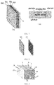
- FIG. 1 and FIG. 2 are schematic structural diagrams of a single-column and multi-row equivalent negative refractive flat lens according to the present disclosure.
- the flat lens includes a pair of glass windows each having two optical films, and two sets of optical waveguide arrays located between the two glass windows.
- the optical waveguide array is composed of single-column and multi-row optical waveguides arranged obliquely at 45° and having a rectangular cross section, and waveguide directions of mutually corresponding parts of the two sets of optical waveguide arrays are perpendicular to each other.
- Such flat lens can enable a two-dimensional or three-dimensional light source to directly generate a real image in air and thus achieve a real holographic image. This can achieve naked eye three-dimensional display characteristics while achieving a large field of view, a large aperture and a high resolution with no distortion and no chromatic dispersion.
- the present disclosure has beneficial effects as follows.
- the present disclosure can greatly reduce individual differences among the traditionally processed strip-shaped optical waveguides and greatly reduce the image cropping defect.
- Two polished surfaces of the strip-shaped optical waveguides are plated with the aluminum films, so that the dependence of the flat lens on types of optical materials is greatly reduced and the requirements of a gluing technology on bubbles and impurities are reduced.
- the requirements for three-dimensional display characteristics and the naked eye three-dimensional holographic display are met, and the purpose of sharp three-dimensional imaging of the spliced array can be truly achieved.
- the present embodiment provides a processing method of a single-column and multi-row equivalent negative refractive flat lens, which includes steps as follows.
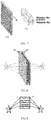
- the present disclosure relates to two single-column and multi-row equivalent negative refractive optical waveguide array plates IM1 and IM2 that are orthogonal to each other, as core imaging elements.
- the present disclosure can achieve point-to-point aberrationless imaging between an object side and an image side.
- the specific principle lies in that a light beam from an object side at side A is reflected inside optical waveguides of the equivalent negative refractive flat lens one or more times, so that the light beam is modulated into mirror image light while being transmitted to an image side at side B, and then the light beam converges to an image again.
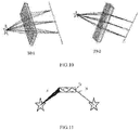
- the IM1 and the IM2 are disassembled, as shown in FIG.
- light beams from a single point at an object side after entering the equivalent negative refractive flat lens from a single side, are subjected to mirror image modulation by respective rows of optical waveguides, and then converge on a straight line parallel to a long side of the optical waveguides again, so as to form a point-to-line one-dimensional imaging effect.
- two sets of optical waveguides are used jointly. To be specific, arrangement directions of the two sets of optical waveguides are perpendicular to each other.
- the point-to-point modulation can be performed on an object image as a target, and the imaging effect is consistent with that of the flat lens made of a negative refractive material (with reference to FIG. 8 ).
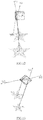
- the optical waveguide according to the present disclosure can only partially modulate the object light, as shown in FIG. 11 , mirror image modulated light b' participates in imaging, and light b will keep characteristics of the original object light to form stray light.
- Each unit formed by a combination of two sets of optical waveguides that are perpendicular to each other is equivalent to one square waveguide for stray light analysis.
- the combined waveguide generates four light beams at the image side, at least two of which reach an image plane, including one participating in imaging and another one affecting imaging as stray light.
- two sets of optical waveguide arrays need to be rotated by 45 ° and orthogonally arranged with respect to each other, so as to eliminate the affection of the stray light, as shown in FIG. 13 .
- the final imaging effect of the imaging principle is consistent with that of a flat lens made of a negative refractive material.
- the embodiments of the present disclosure mainly describe the processing method of the single-column and multi-row equivalent negative refractive flat lens and the imaging principle of the flat lens.
- the equivalent negative refractive flat lens manufactured according to the processing method of the present disclosure there are smaller differences among the individual optical waveguides, so that the image cropping defect caused by the differences among the individual optical waveguides can be greatly reduced.
- the materials used by the flat lens of the present disclosure can be conventional optical materials, and the processing method can achieve high-precision processing in a shorter time.
- the double-sided plating of the strip-shaped optical waveguide can avoid defects such as bubbles, impurities and the like generated in the gluing process, which would otherwise affect the imaging, thereby greatly reducing the difficulty of the gluing process.
- the high-definition imaging can be achieved, and it is easy to achieve mass production is easy with lower cost.
Landscapes
- Physics & Mathematics (AREA)
- Engineering & Computer Science (AREA)
- General Physics & Mathematics (AREA)
- Optics & Photonics (AREA)
- Health & Medical Sciences (AREA)
- Manufacturing & Machinery (AREA)
- Ophthalmology & Optometry (AREA)
- Mechanical Engineering (AREA)
- Multimedia (AREA)
- Signal Processing (AREA)
- Optical Integrated Circuits (AREA)
Applications Claiming Priority (2)
| Application Number | Priority Date | Filing Date | Title |
|---|---|---|---|
| CN201810726637.7A CN110687621A (zh) | 2018-07-04 | 2018-07-04 | 一种单列多排等效负折射率平板透镜的加工工艺 |
| PCT/CN2018/095950 WO2020006780A1 (zh) | 2018-07-04 | 2018-07-17 | 一种单列多排等效负折射率平板透镜的加工工艺 |
Publications (2)
| Publication Number | Publication Date |
|---|---|
| EP3779522A1 true EP3779522A1 (de) | 2021-02-17 |
| EP3779522A4 EP3779522A4 (de) | 2021-06-23 |
Family
ID=69060597
Family Applications (1)
| Application Number | Title | Priority Date | Filing Date |
|---|---|---|---|
| EP18925489.9A Pending EP3779522A4 (de) | 2018-07-04 | 2018-07-17 | Verarbeitungstechnologie für einspaltige und mehrreihige äquivalente feldlinse mit negativem brechungsindex |
Country Status (4)
| Country | Link |
|---|---|
| US (1) | US11977242B2 (de) |
| EP (1) | EP3779522A4 (de) |
| CN (1) | CN110687621A (de) |
| WO (1) | WO2020006780A1 (de) |
Families Citing this family (7)
| Publication number | Priority date | Publication date | Assignee | Title |
|---|---|---|---|---|
| CN110716248B (zh) * | 2018-07-12 | 2021-03-09 | 安徽省东超科技有限公司 | 一种多列多排等效负折射率平板透镜的加工工艺 |
| CN114252941A (zh) * | 2020-09-21 | 2022-03-29 | 郭生文 | 一种光波导透镜 |
| CN113534303B (zh) * | 2021-06-22 | 2022-07-08 | 浙江蓝特光学股份有限公司 | 一种胶合棱镜的加工方法 |
| CN114637127A (zh) * | 2022-02-24 | 2022-06-17 | 安徽省东超科技有限公司 | 应用于光学成像系统的视场控制装置以及光学成像系统 |
| CN114815501B (zh) * | 2022-04-22 | 2025-09-12 | 安徽省东超科技有限公司 | 平板透镜的加工方法 |
| CN116203657A (zh) * | 2023-02-10 | 2023-06-02 | 安徽省东超科技有限公司 | 等效负折射率平板透镜及其制备方法 |
| CN118046605B (zh) * | 2024-02-27 | 2024-08-09 | 湖北五方晶体有限公司 | 一种光学棱镜集成双抛加工工艺 |
Family Cites Families (13)
| Publication number | Priority date | Publication date | Assignee | Title |
|---|---|---|---|---|
| US5150259A (en) | 1990-07-30 | 1992-09-22 | Mitsubishi Rayon Company Ltd. | Optical imaging device |
| CN1103630A (zh) * | 1993-12-10 | 1995-06-14 | 卢大伟 | 转移法制作彩虹玻璃的方法 |
| US6177217B1 (en) * | 1999-07-23 | 2001-01-23 | Eastman Kodak Company | Method and apparatus for precise positioning of arrays with periodic structures |
| JP2004302121A (ja) * | 2003-03-31 | 2004-10-28 | Canon Inc | 立体画像表示装置、及び立体画像撮像装置 |
| CN1600724A (zh) * | 2004-09-29 | 2005-03-30 | 崔建伟 | 一种按太阳高度角选择采光功能玻璃 |
| US10073264B2 (en) * | 2007-08-03 | 2018-09-11 | Lumus Ltd. | Substrate-guide optical device |
| JP5073609B2 (ja) | 2008-08-11 | 2012-11-14 | 日東電工株式会社 | 光導波路の製造方法 |
| CN102109638A (zh) | 2011-03-14 | 2011-06-29 | 浙江大学 | 一种玻璃热极化层中的条形光波导 |
| CN204029962U (zh) | 2014-08-14 | 2014-12-17 | 东南大学 | 基于超材料的折射率梯度平板聚焦透镜 |
| JP6165206B2 (ja) * | 2015-09-08 | 2017-07-19 | 松浪硝子工業株式会社 | 光制御パネルの製造方法、光制御パネル、光学結像装置、及び、空中映像形成システム |
| CN107831558A (zh) * | 2017-12-09 | 2018-03-23 | 安徽省东超科技有限公司 | 多排多列等效负折射率平板透镜 |
| CN107807417A (zh) * | 2017-12-09 | 2018-03-16 | 安徽省东超科技有限公司 | 单列多排等效负折射率平板透镜 |
| CN108233863A (zh) | 2018-03-01 | 2018-06-29 | 成都银顶科技有限公司 | 条形聚光均光太阳能发电技术 |
-
2018
- 2018-07-04 CN CN201810726637.7A patent/CN110687621A/zh active Pending
- 2018-07-17 WO PCT/CN2018/095950 patent/WO2020006780A1/zh not_active Ceased
- 2018-07-17 EP EP18925489.9A patent/EP3779522A4/de active Pending
-
2020
- 2020-09-24 US US17/030,502 patent/US11977242B2/en active Active
Also Published As
| Publication number | Publication date |
|---|---|
| EP3779522A4 (de) | 2021-06-23 |
| CN110687621A (zh) | 2020-01-14 |
| US11977242B2 (en) | 2024-05-07 |
| US20210018658A1 (en) | 2021-01-21 |
| WO2020006780A1 (zh) | 2020-01-09 |
Similar Documents
| Publication | Publication Date | Title |
|---|---|---|
| US11977242B2 (en) | Processing technology for single-column and multi-row equivalent negative refractive index plate lens | |
| US11092888B2 (en) | Processing method for multi-row, multi-column flat lens with equivalent negative refractive index | |
| US11598958B2 (en) | Method of fabricating a symmetric light guide optical element | |
| CN102047169B (zh) | 光学装置和结合光学装置的自动立体显示设备 | |
| WO2019109585A1 (zh) | 多排多列等效负折射率平板透镜 | |
| US20170261755A1 (en) | Three-dimensional display substrate, its manufacturing method and three-dimensional display device | |
| WO2018053684A1 (en) | Three-dimensional display panel, three-dimensional display apparatus having the same, and fabricating method thereof | |
| CN106855655B (zh) | 非对称曲面棱镜影像显示光学系统 | |
| TW201912284A (zh) | 一種適於在雷射加工工藝中使用的F-theta鏡頭 | |
| CN118330903B (zh) | 一种空中成像显示系统 | |
| CN107193115A (zh) | 一种近紫外波段的物像双侧远心光学系统 | |
| CN104813214A (zh) | 一种近红外激光聚焦镜头及激光印刷设备 | |
| CN110286494B (zh) | 光波导单元、阵列及平板透镜 | |
| CN207502759U (zh) | 多排多列等效负折射率平板透镜 | |
| CN110208896B (zh) | 一种新型光波导及应用新型光波导的屏幕 | |
| EP3933465B1 (de) | Optische wellenleitereinheit und anordnung sowie flache linse | |
| CN113504604B (zh) | 一种扩瞳装置及ar设备 | |
| US3749477A (en) | Anamorphic lens system | |
| CN202119964U (zh) | 精细激光扫描f-theta透镜 | |
| CN209746177U (zh) | 一种光学透镜 | |
| CN219302778U (zh) | 一种光机及可穿戴显示设备 | |
| CN118732237B (zh) | 一种沙姆投影镜头及投影设备 | |
| US11977245B2 (en) | Optical waveguide unit, array, and flat lens | |
| CN110262047B (zh) | 光波导单元、阵列及平板透镜 | |
| CN109298510B (zh) | 零视差光学检像系统及成像方法 |
Legal Events
| Date | Code | Title | Description |
|---|---|---|---|
| STAA | Information on the status of an ep patent application or granted ep patent |
Free format text: STATUS: THE INTERNATIONAL PUBLICATION HAS BEEN MADE |
|
| PUAI | Public reference made under article 153(3) epc to a published international application that has entered the european phase |
Free format text: ORIGINAL CODE: 0009012 |
|
| STAA | Information on the status of an ep patent application or granted ep patent |
Free format text: STATUS: REQUEST FOR EXAMINATION WAS MADE |
|
| 17P | Request for examination filed |
Effective date: 20201102 |
|
| AK | Designated contracting states |
Kind code of ref document: A1 Designated state(s): AL AT BE BG CH CY CZ DE DK EE ES FI FR GB GR HR HU IE IS IT LI LT LU LV MC MK MT NL NO PL PT RO RS SE SI SK SM TR |
|
| AX | Request for extension of the european patent |
Extension state: BA ME |
|
| A4 | Supplementary search report drawn up and despatched |
Effective date: 20210521 |
|
| RIC1 | Information provided on ipc code assigned before grant |
Ipc: G02B 3/00 20060101AFI20210517BHEP Ipc: B29D 11/00 20060101ALI20210517BHEP Ipc: G02B 5/136 20060101ALI20210517BHEP Ipc: G02B 30/27 20200101ALI20210517BHEP |
|
| DAV | Request for validation of the european patent (deleted) | ||
| DAX | Request for extension of the european patent (deleted) | ||
| STAA | Information on the status of an ep patent application or granted ep patent |
Free format text: STATUS: EXAMINATION IS IN PROGRESS |
|
| 17Q | First examination report despatched |
Effective date: 20231023 |