EP3779426B1 - Vorrichtung zur elektrochemischen messung einer lösung - Google Patents
Vorrichtung zur elektrochemischen messung einer lösung Download PDFInfo
- Publication number
- EP3779426B1 EP3779426B1 EP19774494.9A EP19774494A EP3779426B1 EP 3779426 B1 EP3779426 B1 EP 3779426B1 EP 19774494 A EP19774494 A EP 19774494A EP 3779426 B1 EP3779426 B1 EP 3779426B1
- Authority
- EP
- European Patent Office
- Prior art keywords
- circuit
- electrode
- capacitor
- solution
- noise
- Prior art date
- Legal status (The legal status is an assumption and is not a legal conclusion. Google has not performed a legal analysis and makes no representation as to the accuracy of the status listed.)
- Active
Links
Images



Classifications
-
- G—PHYSICS
- G01—MEASURING; TESTING
- G01N—INVESTIGATING OR ANALYSING MATERIALS BY DETERMINING THEIR CHEMICAL OR PHYSICAL PROPERTIES
- G01N27/00—Investigating or analysing materials by the use of electric, electrochemical, or magnetic means
- G01N27/26—Investigating or analysing materials by the use of electric, electrochemical, or magnetic means by investigating electrochemical variables; by using electrolysis or electrophoresis
- G01N27/416—Systems
- G01N27/4161—Systems measuring the voltage and using a constant current supply, e.g. chronopotentiometry
-
- G—PHYSICS
- G01—MEASURING; TESTING
- G01N—INVESTIGATING OR ANALYSING MATERIALS BY DETERMINING THEIR CHEMICAL OR PHYSICAL PROPERTIES
- G01N27/00—Investigating or analysing materials by the use of electric, electrochemical, or magnetic means
- G01N27/26—Investigating or analysing materials by the use of electric, electrochemical, or magnetic means by investigating electrochemical variables; by using electrolysis or electrophoresis
- G01N27/416—Systems
- G01N27/48—Systems using polarography, i.e. measuring changes in current under a slowly-varying voltage
-
- G—PHYSICS
- G01—MEASURING; TESTING
- G01N—INVESTIGATING OR ANALYSING MATERIALS BY DETERMINING THEIR CHEMICAL OR PHYSICAL PROPERTIES
- G01N27/00—Investigating or analysing materials by the use of electric, electrochemical, or magnetic means
- G01N27/02—Investigating or analysing materials by the use of electric, electrochemical, or magnetic means by investigating impedance
- G01N27/22—Investigating or analysing materials by the use of electric, electrochemical, or magnetic means by investigating impedance by investigating capacitance
- G01N27/226—Construction of measuring vessels; Electrodes therefor
-
- G—PHYSICS
- G01—MEASURING; TESTING
- G01N—INVESTIGATING OR ANALYSING MATERIALS BY DETERMINING THEIR CHEMICAL OR PHYSICAL PROPERTIES
- G01N27/00—Investigating or analysing materials by the use of electric, electrochemical, or magnetic means
- G01N27/02—Investigating or analysing materials by the use of electric, electrochemical, or magnetic means by investigating impedance
- G01N27/22—Investigating or analysing materials by the use of electric, electrochemical, or magnetic means by investigating impedance by investigating capacitance
- G01N27/228—Circuits therefor
-
- G—PHYSICS
- G01—MEASURING; TESTING
- G01N—INVESTIGATING OR ANALYSING MATERIALS BY DETERMINING THEIR CHEMICAL OR PHYSICAL PROPERTIES
- G01N27/00—Investigating or analysing materials by the use of electric, electrochemical, or magnetic means
- G01N27/26—Investigating or analysing materials by the use of electric, electrochemical, or magnetic means by investigating electrochemical variables; by using electrolysis or electrophoresis
- G01N27/28—Electrolytic cell components
- G01N27/30—Electrodes, e.g. test electrodes; Half-cells
- G01N27/301—Reference electrodes
-
- G—PHYSICS
- G01—MEASURING; TESTING
- G01N—INVESTIGATING OR ANALYSING MATERIALS BY DETERMINING THEIR CHEMICAL OR PHYSICAL PROPERTIES
- G01N33/00—Investigating or analysing materials by specific methods not covered by groups G01N1/00 - G01N31/00
- G01N33/48—Biological material, e.g. blood, urine; Haemocytometers
- G01N33/483—Physical analysis of biological material
- G01N33/487—Physical analysis of biological material of liquid biological material
- G01N33/48707—Physical analysis of biological material of liquid biological material by electrical means
Definitions
- the present disclosure relates to an electrical circuit for electrochemical measurement and a measurement device.
- a chemical substance or a biological substance is detected or quantified by measuring an electric current flowing in a solution by a chemical reaction or a biochemical reaction in which a chemical substance or a biological substance in a solution occurs at or near an electrode surface.
- a method such as three-electrode method is widely used.
- the three-electrode method is a method in which a counter electrode, a reference electrode, and a working electrode are installed in a container, a predetermined potential difference is provided between the counter electrode and the working electrode, and a current flowing from the counter electrode to the working electrode is measured.
- a potential difference called an interfacial potential occurs between the substance and the electrolytic solution.
- the potential at the reference electrode can be measured, and the voltage applied to the counter electrode can be controlled so that the potential is determined to a desired value.
- US 6 228 237 B1 refers to a device for automatically measuring a concentration of a developing agent in a developing bath includes a voltage generator capable of generating at least one voltage ramp provided to feed a three-electrode cell; a potentiostat provided to maintain a constant potential difference between two electrodes; a peak detector provided to identify the maximum current flowing in the three-electrode cell that corresponds to the developing agent concentration; and a display unit provided to show the maximum current.
- US 4 500 391 A refers to an electrochemical detection cell which includes, in the order named, a stack of components constituted by a first membrane, an electrode carrier having reference and counter electrodes thereon, a membrane support, an electrode carrier having a sensing electrode thereon, and a permselective membrane.
- US 5 470 484 A refers to a method for controlling the chemical treatment of a solution comprises the steps of feeding a treatment chemical into the solution, applying an external voltage across a reference electrode and a working electrode of a voltammetric sensor while the electrodes are immersed in the solution, measuring a current that flows through the working electrode, converting the measured current into a feedback signal indicative of the concentration of treatment chemical in the solution, and using the feedback signal to control the rate of feeding the treatment chemical.
- a device for an electrochemical measurement of a solution, comprising:
- the source of external noise is relatively easy to identify. Therefore, if the propagation path from the source of the noise to the measurement unit is cut off, it is possible to reduce the effect. For example, if the measuring system is covered with a shield, the effects of noise, static electricity, and communication radio waves propagating from external equipment can be greatly reduced. Further, the influence of noise caused by commercial power supply, switching power supply, clock, etc. entering the inside of the measuring device can be reduced by appropriately placing the ground of the measuring device. Alternatively, with the exception of static electricity and commercial power supplies, these noises can be reduced by a low-pass filter (LPF) or the like because of their high frequency. In addition, the frequency of commercial power supply is determined by the country and region to be 50Hz or 60Hz.
- LPF low-pass filter
- the averaging process in accordance with the period e.g., averaging the data for 0.1 seconds, the signal of 50Hz/60Hz becomes zero
- the countermeasure can be sufficiently carried out by properly applying the shield.
- noise such as thermal noise, shot noise, flicker noise (1/f noise).
- thermal noise shot noise
- these noises can not be reduced by proper arrangement of the shield or ground, because they are present inside the device or electrical or electronic elements in the measuring device. Further, these noises are present at low frequency, and thus may be difficult to reduce in the averaging process. In particular, flicker noise (1/f noise) is difficult to reduce in the averaging process since its noise power is increased at low frequencies.
- the body fluid may be lymph fluid, tissue fluid such as interstitial fluid, intercellular fluid, or interstitial fluid, and may be body cavity fluid, serosal fluid, pleural fluid, ascites fluid, effusions, cerebrospinal fluid, joint fluid (synovial fluid), or aqueous humor of eye (aqueous humor).
- the body fluid may be digestive fluid such as saliva, gastric juice, bile, pancreatic juice, intestinal fluid, etc., and may be sweat, tears, nasal mucus, urine, semen, vaginal fluid, amniotic fluid, milk, etc.
- the solution may be a physiological buffer such as phosphate buffered saline (PBS) or N-tris(hydroxymethyl)methyl-2-aminoethanesulfonic acid buffer (TES), containing a substance to be measured.
- PBS phosphate buffered saline
- TES N-tris(hydroxymethyl)methyl-2-aminoethanesulfonic acid buffer
- the electrochemical measurement method may be an amperometric method during electrolysis.
- the amperometry may measure the current value when the potential is kept constant, or the voltammetry may measure the variation of the current amount when the potential is varied.
- the electrochemical measurement method may be a three-electrode method.
- the voltage generating circuit may include a power supply, or may be configured to convert the voltage from a power supply provided at its outside to a desired voltage. It may include a circuit for dividing the power supply voltage, or it may include an integrated circuit (IC) capable of generating a desired voltage.
- the voltage generating circuit may be configured to have a low-pass filter circuit and a buffer circuit.
- the output of the operational amplifier (OUT) and the counter electrode (CE) may be directly connected, or a resistor of, for example, 100 ⁇ (ohms) may be connected in series between the output of the operational amplifier (OUT) and the counter electrode (CE) so as not to damage the electronic elements in the circuit by making a connection error.
- the output of the operational amplifier may not be directly connected to the counter electrode.
- an amplifier circuit or an attenuation circuit may further be connected in the subsequent stage.
- multiple stages of operational amplifiers may be used for connection.
- a protective resistor may be placed in series to form the connection.
- the capacitor is connected between the output (OUT) and the inverting input (-IN) via the switch.
- the capacitor may have a capacitance of 1 ⁇ F or greater. In another embodiment, the capacitor may have a capacitance greater than 1 ⁇ F.
- the capacitance of the capacitor may be greater than or equal to 2 ⁇ F, 3 ⁇ F, 4 ⁇ F, 5 ⁇ F, 6 ⁇ F, 7 ⁇ F, 8 ⁇ F, 9 ⁇ F, or 10 ⁇ F, or may be greater than any value thereof.
- the capacitance of the capacitor may be greater than or equal to 10 ⁇ F, 20 ⁇ F, 30 ⁇ F, 40 ⁇ F, 50 ⁇ F, 60 ⁇ F, 70 ⁇ F, 80 ⁇ F, 90 ⁇ F, or 100 ⁇ F, or may be greater than any value thereof.
- the capacitance of the capacitor may be greater than the capacitance of the equivalent circuit at the interface of the counter electrode under measurement.
- the capacitor may be a noise reduction capacitor.
- the contact area of the electrode with the solution may be less than or equal to 100 square millimeters.
- the capacitance of the electrode interface may generally be about 10 ⁇ F or smaller.
- the thickness of the electric double layer may be as small as 1 nm or greater than this.
- the capacitance of the capacitor is 10 ⁇ F, noise can sufficiently be reduced. Further, if the capacitance of the capacitor is 100 ⁇ F, noise can be further reduced. For example, if the electrode area is further smaller, the capacitance of the capacitor may be 0.1 ⁇ F.
- the capacitance of the capacitor may be smaller than or equal to 100mF, 10mF, 1mF, 500 ⁇ F, 400 ⁇ F, 300 ⁇ F, 200 ⁇ F, 100 ⁇ F, or may be smaller than any value thereof.
- the capacitance of the capacitor may be 350 ⁇ For 330 ⁇ F.
- the capacitor may be a ceramic capacitor.
- the capacitor may be configured by combining two or more capacitors. For example, two electrolytic capacitors may be connected in series in opposite directions.
- the capacitor may or may not have polarity. Non-polar capacitors are useful when the voltage applied to them may vary between positive and negative.
- the counter electrode, the reference electrode, and the working electrode may be referred to as an electrode, and may be referred to as a counter electrode, a reference electrode, and a working electrode, respectively.
- the working electrode at least on a surface in contact with the solution, may be formed of a metal such as platinum (Pt), gold (Au), silver (Ag), or copper (Cu), may be a carbon electrode including carbon nanotubes, graphene, diamond, or the like, may be a metal oxide such as tantalum oxide, or may be a conductive polymer.
- Current measuring circuit may have a current-voltage conversion circuit.
- the current measurement circuit may be configured with a current-voltage conversion circuit and a voltage measurement circuit connected in series.
- the voltage measurement circuit may be an A/D converter.
- nodal point or a node a point where a plurality of circuit elements or wires are connected is called a nodal point or a node, often represented by a point of black circle
- nodal point or node as well as locations such as wiring sections that can be treated as substantially the same potential for circuit function, with the exception of the electrical and electronic circuitry or elements explicitly shown, are called a node.
- the output of the voltage generating circuit 20 is connected to the non-inverting input (+IN) of the operational amplifier 30, and supplies a reference voltage Vref.
- the voltage generating circuit 20 supplies an output signal having the stable potential difference Vref with respect to the ground potential of the measuring device 1.
- the output of the operational amplifier 30 is connected to the counter electrode 91, and the inverting input (-IN) is connected to the reference electrode 92.
- the capacitor 40 is connected between the counter electrode 91 and the reference electrode 92, or between the output (OUT) and the inverting input (-IN) of the operational amplifier 30. In other words, the capacitor 40 is connected to the output of the operational amplifier 30 (OUT) and the counter electrode 91 at one end, and is connected to the inverting input (-IN) and the reference electrode 92 of the operational amplifier 30 at the other end.
- the current measuring circuit 50 is connected to the working electrode 93 and receives the value of the current from the working electrode 93 and outputs an output signal to the outside of the electric circuit 10.
- a substantially equipotential wiring section between the output (OUT) of the operational amplifier 30 and the capacitor 40, or between the output (OUT) of the operational amplifier 30, the capacitor 40, and the counter electrode 91 is referred to as a node (first node) 11.
- a substantially equipotential wiring section between the inverting input (-IN) of the operational amplifier 30 and the capacitor 40, or between the inverting input (-IN) of the operational amplifier 30, the capacitor 40 and the reference electrode 92 is referred to as a node (second node) 12.
- a substantially equipotential wiring section between the working electrode 93 and the current measuring circuit is referred to as a node (third node) 13.
- the container 90 containing the solution 95, the counter electrode 91, the reference electrode 92, and the working electrode 93 may be configured to be removed from the measuring device 1.
- the container 90 containing the solution 95, the counter electrode 91, the reference electrode 92, and the working electrode 93 may be configured to be disposable at each measurement, according to the frequency of use or according to the time interval.
- the container 90 containing the solution, the counter electrode 91, the reference electrode 92, and the working electrode 93 may be fitted into the measurement device 1 such that the counter electrode 91, the reference electrode 92, and the working electrode 93 may be configured to form electrical contact with the first node 11, the second node 12, and the third node 13, respectively.
- the container 90 containing the solution, the counter electrode 91, the reference electrode 92, and the working electrode 93 may be integrally formed or manufactured in the measuring device 1.
- the measuring device 1 includes a shield 60.
- Shield 60 can reduce external noise.
- the shield 60 is disposed so as to surround the electric circuit 10, the container 90, the counter electrode 91, the reference electrode 92, and the working electrode 93, but the arrangement of the shield 60 is not limited thereto.
- the shield 60 may be disposed along or surrounding the second node 12.
- the wiring configured to be connected to the output (OUT) of the operational amplifier 30, the inverting input (-IN) of the operational amplifier 30, and the current measurement circuit 50 may be configured to be connected to the counter electrode 91 (CE), the reference electrode 92 (RE), and the working electrode 93 (WE) that are in contact with the solution during the electrochemical measurement, respectively.
- the measuring device 1 and the electrical circuit path 10 may be configured such that the component including the electrical circuit and the component including the counter electrode (CE), the reference electrode (RE), and the working electrode (WE) are in contact or merged in a form of a mechanical fit or the like to form electrical contact with the respective wires of the counter electrode 91 (CE), the reference electrode 92 (RE), and the working electrode 93 (WE).
- the container 90 containing the solution 95 may be configured to be removal with respect to the measuring device 1 in a cartridge manner.
- the container 90 may have an inlet for introducing a solution 95 or other liquid.
- the container 90 may have an outlet for discharging the solution 95 and other liquids.
- Each of the inlet and the outlet may be one or plural, and may be configured as the same hole.
- the counter electrode 91 (CE), the reference electrode 92 (RE), and the working electrode 93 (WE) may be secured to the container 90 and removably fixable to the container 90.
- the container 90 may be configured to contain solution 95 in a substantially non-flowing state during measurement.
- the container 90 may be configured as a channel.
- the solution 95 is flowed into or introduced into the container 90 from the introduction port or inlet (not shown).
- the substance to be measured or the measurement object substance may be contained in the solution in advance, or may be mixed into the solution 95 after the solution containing no substance to be measured is introduced into the container 90, at a different timing.
- the timing at which the substance to be measured and the solution are mixed is not limited thereto.
- a solution 95 in which a substance to be measured is dissolved may be poured into the container 90 from a state in which the counter electrode 91, the reference electrode 92, and the working electrode 93 are not in contact with the solution 95, that is, from a dry state.
- the introduced solution 95 contacts at least a portion of the surface of the counter electrode 91, the reference electrode 92, and the working electrode 93
- a feedback loop is formed that returns from the output of the operational amplifier 30, via the first node 11, the counter electrode 91, the solution 95, the reference electrode 92, and the second node 12, back to the inverting input (-IN) of the operational amplifier 30.
- the voltage of the counter electrode 91 is controlled so that the voltage transmitted from the reference electrode 92 to the second node 12 is equal to the reference voltage Vref.
- the operational amplifier 30 is one component of the feedback circuit, another circuit component having similar functions may be used in another embodiment.
- Capacitor 40 can reduce the effects of noise inherent in the components of the device, such as thermal noise, shot noise, flicker noise, and the like (hereinafter referred to as "physical noise").
- the physical noise is inherent in the components of the voltage generating circuit 20 and the operational amplifier 30.
- the physical noise inherent in the components of the voltage generating circuit 20 is superimposed on the reference voltage signal as voltage noise is input to the non-inverting input terminal of the operational amplifier 30 (+IN).
- Physical noise inherent in the operational amplifier 30 is present in both the inverting input (-IN) and the non-inverting input (+IN), but equivalently can be calculated as the sum is present concentrated on the non-inverting input (+IN) of the operational amplifier 30.
- the noise of the operational amplifier 30 is superimposed on the reference voltage signal. From these, the physical noise present at various locations can be considered as one noise summed on the non-inverting input (+IN) of the operational amplifier 30 superimposed on the reference voltage Vref. This is hereinafter also referred to as "integrated physical noise".
- interface impedance The ones that constitute the interfacial impedance are redox reactions and electric double layers.
- the oxidation reduction (redox) reaction generates the transfer of electrons between the solution and the electrode, whereby a direct current flows.
- the electric double layer is formed by ions that collect at the interface and does not generate transfer of electrons.
- the oxidation-reduction reaction can be expressed as a resistor, and the electric double layer can be expressed as a capacitor. Therefore, the interface impedance can be approximately expressed as a parallel circuit of these.
- the interface impedance can be approximately expressed as a parallel circuit of these.
- there are complex elements such as Warburg impedance dominated by the diffuse rate.
- the counter electrode 91, the reference electrode 92, and the working electrode 93 each have an interface impedance, and each can be approximately expressed as a parallel circuit of resistance and capacitance.
- the integrated physical noise is amplified by the feedback loop.
- the mechanism will be described below.
- the amount of feedback from the operational amplifier output to the inverting input is determined by the impedance division Zw/ (Zc+Zw) with the interface impedance Zc between the counter electrode 91 and the solution 95, and the interface impedance Zw between the working electrode 93 and the solution 95.
- the impedance Zr of the equivalent circuit there is a path through the impedance Zr of the equivalent circuit at the interface of the reference electrode 92 and the solution 95.
- the impedance Zr at the reference electrode 92 may be considered not to affect the impedance division in the feedback path.
- the input impedance of a general operational amplifier is sufficiently large compared to the value of Zc and Zw obtained realistically.
- the input impedance of the current measuring circuit 50 may be considered sufficiently small.
- the ammeter is required to have a low input impedance.
- the current-voltage conversion circuit 51 has a virtual ground at the input unit, the input impedance may be regarded as zero.
- Electrochemical measurements such as the three-electrode method, currents due to chemical or biochemical reactions by minute amounts of substances contained in the solution are measured. In order to obtain more current, it is effective to increase the contact area of the working electrode with the solution. Generally, the area of the working electrode is larger than the area of the counter electrode. When the contact area is large, the impedance of the interface becomes small, and the capacitance becomes large.
- the area of the working electrode was about 2.5 times the area of the counter electrode, and the equivalent circuits of the interface of the counter electrode, the reference electrode, and the working electrode were 35 M ⁇ //2.8 ⁇ F, 2 M ⁇ //1.4 ⁇ F, and 14 M ⁇ //7 ⁇ F, respectively.
- "//" indicates that the left and right elements are connected in parallel.
- the time required for the measurement is about 0.1 second to about 1 minute, and the frequency is in the range of about 0.01 Hz to 10 Hz.
- the impedance is substantially proportional to the inverse of the capacitance, since the capacitance is dominant in the equivalent circuit of the interface. If the input impedance of the inverting input (-IN) of the operational amplifier 30 is sufficiently large, Zr can be ignored if there is no capacitor 40, the amplification factor of the noise in the feedback loop can be expressed as (Zc+Zw)/Zw.
- the capacitor 40 is connected to the first node 11 which is the output of the operational amplifier 30 and the second node 12 which is the inverting input (-IN) of the operational amplifier 30.
- the capacitor 40 is arranged in parallel with a path from the first node 11 which is the output (OUT) of the operational amplifier 30, via the counter electrode 91, the solution 95, and the reference electrode 92, back to the second node 12 which is the inverting input (-IN) of the operational amplifier 30. Therefore, the feedback amount of the feedback loop is increased as compared to when there is no capacitor 40.
- the noise power appearing at the counter electrode 91 via the first node 11 is reduced, and it is possible to improve the measurement accuracy of the minute current.
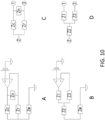
- connection of Zc, Zr, and the impedance Zn of and the capacitor 40 is regarded as a ⁇ -type connection ( FIG. 10A ), which can be converted into T-type connection ( FIG. 10B ). More specifically, ⁇ -type connection of Zc, Zr, Zn shown in FIG. 10C can be converted to T-type connection of Z1, Z2, Z3 shown in FIG. 10D .
- Z1 (Zc ⁇ Zn)/(Zr+Zn+Zc)
- Z2 (Zr ⁇ Zc)/(Zr+Zn+Zc)
- Z3 (Zn ⁇ Zr)/(Zr+Zn+Zc).
- the feedback amount of the feedback loop can be expressed as (Z2+Zw)/(Z1+Z2+Zw)
- the amplification factor of the noise can be expressed as (Z1+Z2+Zw)/(Z2+Zw).
- the amplification factor of the non-inverting amplifier of the feedback loop is reduced, the amplification factor of the integrated physical noise present in the non-inverting input (+IN) of the operational amplifier 30 is reduced.
- the feedback amount increases.
- the capacitances Cc and Cw of the counter electrode 91 and the working electrode 93 described above are used as they are and the capacitance Cn of the capacitor 40 is 100 ⁇ F, most of the feedback is performed through the capacitor 40, so that the feedback amount becomes almost 1 and the noise is not amplified. That is, as compared with the case without the capacitor 40 it leads to 3.5 times of the noise reduction.
- Noise caused by external noise with a relatively high frequency can be reduced by averaging in accordance with countermeasures for shielding and ground.
- noise with relatively low frequency cannot be expected to be reduced by techniques such as averaging.
- physical noise cannot be reduced in the shield or ground because it is inherent in the parts.
- attempting to reduce physical noise with low frequency by averaging may also reduce the original signal.
- flicker noise which increases inversely proportionally to the frequency, is the dominant noise at low frequencies. Flicker noise in the vicinity of the time constant of the electrochemical reaction is very difficult to remove by conventional methods.
- the electric circuit including the capacitor 40 and the feedback circuit thereof can remarkably enhance the effect of noise reduction in the frequency range of, for example, about 0.01 Hz to 10 Hz.
- the electrical circuit and its feedback circuit having the capacitor 40 for example, can increase the feedback amount of noise having a frequency of about 10 Hz from 0.01 Hz, and thus the amplification of noise in the feedback circuit is suppressed.
- chemical reactions may take from 0.1 seconds to about 1 minute or more.
- the electrical circuit including the capacitor 40 of the present disclosure can improve the accuracy of the electrochemical measurement.
- the current measuring circuit 50 may be provided with a current-voltage conversion circuit 51.
- the current-voltage conversion circuit 51 may be configured using an operational amplifier and a resistor. At this time, the inverting input of the operational amplifier is a virtual ground. The input impedance of the third node 13 is low and can be considered zero.
- Measuring device 1 may have an analog-to-digital (A/D) conversion circuit 52 inside the current-voltage conversion circuit 50 ( FIG.8 ) or outside thereof. In the current measuring circuit 50 shown in FIG. 8 , the current signal from the working electrode 93 is current-voltage converted by the current-voltage conversion circuit 51, converted into digital data by the A/D converter 52, and output as a digital signal to the outside of the electric circuit 10.
- A/D analog-to-digital
- the counter electrode 91 is an electrode having a predetermined voltage difference between it and the working electrode 93.
- the voltage difference may be determined according to the type of electrode used for measurement or the substance to be measured.
- a voltage as high as possible may be applied within a range in which an excessive load is not applied to the molecular recognition film.
- the potential difference between the counter electrode 91 and the solution 95 changes in accordance with the amount of current flowing. Therefore, in order to keep the potential of the solution 95 at a predetermined value, the potential of the solution is measured by the reference electrode 92, and the potential of the counter electrode 91 is controlled by the feedback circuit.
- a molecular recognition film that specifically reacts with a substance to be measured is provided on a surface of the working electrode 93 (not shown)
- the molecular recognition film may include a polymer film.
- the polymer film may be, for example, a biomolecule such as an antigen, an antibody, an enzyme, or the like, a self-assembled monomolecular film (SAM : Self-Assembled Monolayer), a polymer film such as a molecular template polymer (MIP : Molecular Imprinted Polymer), or the like, depending on the substance to be measured.
- SAM Self-Assembled Monolayer
- MIP molecular template polymer
- the shield 60 is made of an electrically conductive material including, for example, a metal.
- the shield 60 may block noise entering from outside the equipment.
- by setting the shield to the same as the ground potential it is also possible to reduce the noise generated in the internal circuit such as commercial power supply noise and switching noise.
- the voltage generating circuit 20 generates a reference voltage Vref, and supply this to the operational amplifier 30.
- the operational amplifier 30 performs control of the output voltage so that the reference electrode 92 is at the reference voltage Vref.
- a chemical reaction is performed at the working electrode 93.
- the counter electrode 91 a platinum electrode having an area of about 4 square millimeters was used.
- the working electrode 93 a platinum electrode of about 10 square millimeters was used, and a fructosylamino acid oxidase (FAOD) enzymatic film for measuring glycoalbumin was formed on this surface.
- the reference electrode 92 a platinum electrode of about 2 square millimeters was used, and silver chloride was disposed on the surface of the platinum electrode.
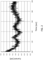
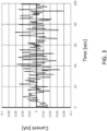
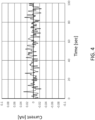
- FIGS. 2 , 3 and 4 show a noise waveform measured without the noise countermeasure according to the present disclosure.
- FIG. 3 shows the noise waveform when taking measures to reduce external noise by performing such shielding and appropriate ground arrangement.
- FIG. 4 shows a noise waveform when placing a capacitor of 10 ⁇ F as the capacitor 40 according to the present disclosure.
- noise of the order of 0.7 nA (nanoampere) p-p (peak to peak) was observed when no noise countermeasures were taken.
- noise of about 0.12 nAp-p was observed when measures to reduce external noise were taken. The influence of external noise almost disappeared, and the physical noise became dominant for the observed noise. However, the amplification effect in the feedback loop was observed.
- noise was reduced to about 0.04 nAp-p when an electric circuit including a noise reduction capacitor was used.
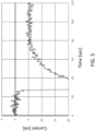
- FIGS. 5 and 6 show an example of a current waveform when taking measures to reduce external noise by performing such shielding and appropriate ground arrangement.
- FIG. 6 shows a current waveform when placing a capacitor of 10v ⁇ F as a capacitor 40.
- FIGS. 5 and 6 show the replacement of solutions at the 28-second and 32-second time points in each graph.
- the current value increased rapidly.
- the downward direction of the graph means an increase in current in relation to the measurement system.
- the current stabilized. It is considered that such a peak current is generated by a factor other than a desired chemical reaction, such as the formation of an electric double layer or the variation of the concentration distribution of ions in the solution or the like. This peak current makes it difficult to measure the current corresponding to the chemical reaction to be measured. Therefore, it is preferable to measure a stable current after the peak current or the rapid change of the current has disappeared.
- the concentration of glycoalbumin in tears of about 10 ⁇ L is about 1 mg/mL. Therefore, quantification of glycoalbumin in tears requires accurate measurement of this degree of current.
- the current value at the time of stability is about 5 to 10 nA. It is required to measure this value with an accuracy of 1% units, i.e. an accuracy of 0.05 nA to 0.1 nA or so. In the measurement of FIG. 5 , it is almost impossible to ensure an accuracy of 1% of the current value. On the other hand, in the measurement of FIG. 6 , it is possible to reduce the influence of noise to 1% or less. In addition, time averaging may be used. This can further increase the measurement accuracy.
- the current flowing from the counter electrode to the working electrode changes, and the potential of the counter electrode 91 changes accordingly. Since the potential of the reference electrode 92 is constant, the potential difference applied across the capacitor 40 is changed. Since this change requires the injection of charge, the capacitor 40 needs to be charged during the measurement. At this time, the charge injected into the capacitor 40 only passes through the second node 12 from the reference electrode 92. The current injected from reference electrode 92 is limited by the electrical resistance of reference electrode 92. That is, the injection time of charge into the capacitor 40 is determined by the electrical resistance of the reference electrode 92 and the capacitance of the capacitor 40.
- the capacitance of the capacitor 40 is 10 ⁇ F, and the electrical resistance of the reference electrode 92 is about 2 M ⁇ , the time constant of charging of the capacitor 40 is 20 seconds. Therefore, this configuration, while achieving an effect of suppressing noise, it is possible to avoid or reduce the waiting time of charging of the capacitor 40 which is a large hindrance to the measurement. In other words, it is possible to achieve both the improvement of the measurement accuracy of the minute current, and the suppression of the measurement time.
- the capacitance of the capacitor 40 may be 100 ⁇ F or larger.
- the impedance Zn of the capacitor 40 is further reduced, further improving the feedback amount of noise, and further suppressing the amplification of noise.
- FIG. 7 is a circuit block diagram showing an example of the configuration of the measurement apparatus according to the invention.
- the measuring device 101 shown in FIG. 7 includes an electric circuit 110, a container 90 containing a solution 95, a counter electrode 91, a reference electrode 92, a working electrode 93, a shield 60, and a housing 70.
- the electric circuit 110 includes a voltage generating circuit 20, an operational amplifier 30, a capacitor 40, a switch (switch circuit) 180, and a buffer circuit 181.
- the electrical circuit 110 includes a voltage generating circuit 20, a operational amplifier 30, a capacitor 40, a current measuring circuit 50, and a capacitor charging circuit (not shown).
- the time to charge the capacitor 40 by the capacitor charging circuit may be less than or equal to any value of 1 second, 5 seconds, 10 seconds, 30 seconds, 1 minute, 2 minutes, 3 minutes, 4 minutes, 5 minutes, 10 minutes, 15 minutes, 30 minutes, 60 minutes.
- the capacitor 40 shown in FIG. 7 is provided between the first node 11 and the switch 180. That is, the capacitor 40 has one end connected to the output (OUT) of the operational amplifier and the first node 11, and the other end connected to the output terminal 180c of the switch circuit 180.
- the switch 180 is a circuit block having a first input terminal 180a, a second input terminal 180b, and an output terminal 180c.
- the switch 180 has a control unit (not shown), which can switch the connection of the two input terminals by the control unit.
- the first input terminal 180a is connected to the output terminal of the buffer circuit 181.
- the second input terminal 180b is connected to the inverting input (-IN) of the operational amplifier 30 and the reference electrode 92, that is, to the second node 12.
- the output terminal 180c is connected to one end of the capacitor 40.
- the switch 180 can switch the connection destination of the capacitor 40 by switching the connection of the input terminal.
- Buffer circuit 181 is a circuit that receives the input voltage at a high impedance, and outputs the same voltage as the input voltage at a low impedance.
- the buffer circuit 181 shown in FIG. 7 is connected at its output terminal to the first input terminal 180a of the switch circuit 180.
- the input terminal is connected to the inverting input (-IN) and to the reference electrode 92, i.e. to the second node 12.
- the buffer circuit 181 receives the voltage of the reference electrode 92 and the second node 12 with a high impedance, and charges the capacitor 40 with a low impedance.
- the buffer circuit 181 may be a voltage follower using an operational amplifier. However, the configuration of the buffer circuit 181 is not limited thereto and may be different.
- the capacitance of the capacitor 40 may be greater than the interface capacitance of the counter electrode 91 and the interface capacitance of the reference electrode 92.
- the charging time of the capacitor 40 may be longer than the time until the chemical reaction becomes stable.
- the capacitor 40 may also delay the progress of the chemical reaction. Electrochemical measurements cannot be performed correctly while the capacitor 40 is being charged. Therefore, the time while the capacitor 40 is charged is a waiting time. Therefore, it is necessary to set the measurement time longer than when there is no capacitor 40, in other words, it is necessary to set the measurement time sufficiently long including the waiting time for charging of the capacitor 40.
- the time constant calculated as a simple CR product is 20 seconds, 200 seconds, respectively. These time constants may affect chemical and biochemical reactions.
- the reduction of the amplification factor of the noise and the minimization of the influence on the reaction and the shortening of the measurement time can become a trade-off relationship.
- both noise reduction effects and measurement times can be sacrificed a little.
- the capacitance of the optimum noise reduction capacitor is different. For example, since the electrode to be used may be different depending on the substance to be measured, the electrode to be used, the molecular recognition film, the concentration of the measurement substance in the solution or the solution at the time of measurement, and the concentration to be measured, it may become necessary to replace the capacitor for reducing noise.
- the electric circuit 110 having the buffer circuit 181 and the switch 180 as in the present embodiment potentially achieves the following effects. That is, before the chemical reaction is stabilized, that is, before the measurement is started, the output terminal 180c and the input terminal 180a of the switch 180 are connected in accordance with a signal from the control unit. Thus, the switch 180 connects the output terminal of the capacitor 40 and the buffer circuit 181. Therefore, the capacitor 40 can be rapidly charged to a predetermined voltage by the configuration of the electric circuit including the buffer 181 until the chemical reaction is stabilized. During charging, the capacitor 40 does not become a component of the feedback loop and therefore does not affect the chemical and biochemical reactions nor the convergence time of the feedback circuit.
- the output impedance of the buffer circuit 181 can be smaller than or equal to 1 ⁇ , which allows the charging time of the capacitor 40 to be smaller than or equal to 100 ⁇ sec (microseconds).
- the chemical reaction settled in about 1 minute. In such a case, if the charging time is about 1 second to a few seconds, it is not a major problem for measurements. If the chemical reaction settles in about 5 seconds, the time constant of the circuit can be 100 msec.
- the control unit switches the switch 180, to connect the capacitor 40 and the second node 12. At this time, the capacitor 40 is charged to the same voltage as the voltage of the second node 12 by the buffer 181. Therefore, there is no need to re-converge the feedback circuit by switching, achieving noise reduction at the time of measurement as one effect.
Landscapes
- Health & Medical Sciences (AREA)
- Chemical & Material Sciences (AREA)
- Life Sciences & Earth Sciences (AREA)
- Physics & Mathematics (AREA)
- General Physics & Mathematics (AREA)
- Pathology (AREA)
- Immunology (AREA)
- Analytical Chemistry (AREA)
- Biochemistry (AREA)
- General Health & Medical Sciences (AREA)
- Electrochemistry (AREA)
- Chemical Kinetics & Catalysis (AREA)
- Molecular Biology (AREA)
- Engineering & Computer Science (AREA)
- Biomedical Technology (AREA)
- Biophysics (AREA)
- Hematology (AREA)
- Urology & Nephrology (AREA)
- Food Science & Technology (AREA)
- Medicinal Chemistry (AREA)
- Investigating Or Analyzing Materials By The Use Of Electric Means (AREA)
Claims (5)
- Vorrichtung (1, 101) zur elektrochemischen Messung einer Lösung (95), umfassend:eine Gegenelektrode (CE) (91), ausgelegt zum Kontaktieren der Lösung (95);eine Referenzelektrode (RE) (92), ausgelegt zum Kontaktieren der Lösung (95);eine Arbeitselektrode (WE) (93), ausgelegt zum Kontaktieren der Lösung (95);eine Spannungserzeugungsschaltung (20);eine Strommesschaltung (50), die mit der Arbeitselektrode (WE) (93) verbunden ist;einen Operationsverstärker mit einem Ausgang (OUT), einem nichtinvertierenden Eingang (+IN) und einen invertierenden Eingang (-IN),wobei der Ausgang (OUT) mit der Gegenelektrode (CE) (91) verbunden ist,wobei der nichtinvertierende Eingang (+IN) mit der Referenzelektrode (RE) (92) verbunden ist,wobei der invertierende Eingang (-IN) mit der Spannungserzeugungsschaltung (20) verbunden ist;einen Kondensator (40) mit einer Kapazität von 1 µF oder mehr;dadurch gekennzeichnet, dass sie Folgendes umfasst:eine Umschaltschaltung (180) mit einem ersten Eingangsanschluss, dem zweiten Eingangsanschluss und dem Ausgangsanschluss; undeine Pufferschaltung (181) mit einem Eingang und einem Ausgang,wobei der Kondensator (40) an einem Ende mit dem Ausgang des Operationsverstärkers (OUT) und der Gegenelektrode (CE) (91) verbunden ist und an dem anderen Ende mit dem Ausgangsanschluss der Umschaltschaltung (180) verbunden ist,wobei die Umschaltschaltung (180) an dem ersten Eingangsanschluss mit dem Ausgangsanschluss der Pufferschaltung (181) verbunden ist und an dem zweiten Eingangsanschluss mit dem invertierenden Eingang des Operationsverstärkers (-IN) und der Referenzelektrode (RE) (92) verbunden ist,wobei die Pufferschaltung (181) an einem Eingangsanschluss mit dem invertierenden Eingang (-IN) des Operationsverstärkers und der Referenzelektrode (RE) (92) verbunden ist.
- Elektromechanische Messvorrichtung (1, 101) nach Anspruch 1,
wobei die Lösung (95) eine zu messende Substanz enthält, wobei die Vorrichtung (1, 101) ferner einen Molekularerkennungsfilm umfasst, der auf einer Oberfläche bereitgestellt ist, um zumindest mit der Lösung (95) der Arbeitselektrode (93) in Kontakt zu treten, und der insbesondere mit der zu messenden Substanz reagiert. - Elektrische Schaltung (10, 110) nach Anspruch 1 oder 2, wobei die Kapazität des Kondensators (40) 10 µF oder mehr beträgt.
- Elektrische Schaltung (10, 110) nach einem der Ansprüche 1 bis 3, wobei die Kapazität des Kondensators (40) 100 µF oder mehr beträgt.
- Elektrische Schaltung (10, 110) nach einem der Ansprüche 1 bis 4, wobei die Kapazität des Kondensators (40) größer ist als die Kapazität einer Ersatzschaltung an der Grenzfläche der Gegenelektrode (91) unter Messung.
Applications Claiming Priority (2)
| Application Number | Priority Date | Filing Date | Title |
|---|---|---|---|
| JP2018066582 | 2018-03-30 | ||
| PCT/JP2019/012350 WO2019188896A1 (ja) | 2018-03-30 | 2019-03-25 | 電気化学測定用電気回路および測定装置 |
Publications (3)
| Publication Number | Publication Date |
|---|---|
| EP3779426A1 EP3779426A1 (de) | 2021-02-17 |
| EP3779426A4 EP3779426A4 (de) | 2021-12-15 |
| EP3779426B1 true EP3779426B1 (de) | 2023-12-27 |
Family
ID=68059141
Family Applications (1)
| Application Number | Title | Priority Date | Filing Date |
|---|---|---|---|
| EP19774494.9A Active EP3779426B1 (de) | 2018-03-30 | 2019-03-25 | Vorrichtung zur elektrochemischen messung einer lösung |
Country Status (5)
| Country | Link |
|---|---|
| US (1) | US11536690B2 (de) |
| EP (1) | EP3779426B1 (de) |
| JP (1) | JP7239201B2 (de) |
| CN (1) | CN112166318B (de) |
| WO (1) | WO2019188896A1 (de) |
Family Cites Families (13)
| Publication number | Priority date | Publication date | Assignee | Title |
|---|---|---|---|---|
| US4500391A (en) * | 1983-10-13 | 1985-02-19 | Allied Corporation | Method of and system for real time differential pulse detection |
| US4496454A (en) * | 1983-10-19 | 1985-01-29 | Hewlett-Packard Company | Self cleaning electrochemical detector and cell for flowing stream analysis |
| US5180968A (en) * | 1991-03-01 | 1993-01-19 | Research Foundation Of State University Of New York | Method and apparatus for compensation of double layer charging current in electrochemical cells |
| US5470484A (en) * | 1994-01-13 | 1995-11-28 | Buckman Laboratories International, Inc. | Method and apparatus for controlling the feed of water treatment chemicals using a voltammetric sensor |
| GB9708786D0 (en) | 1997-05-01 | 1997-06-25 | Central Research Lab Ltd | Elecrochemical sensing circuits |
| FR2776071B1 (fr) * | 1998-03-13 | 2000-05-26 | Eastman Kodak Co | Dispositif de mesure automatique de la concentration d'un agent developpateur |
| US7914655B2 (en) * | 2003-05-13 | 2011-03-29 | Siemens Aktiengesellschaft | Potentiostatic circuit arrangement on a biosensor for digitisation of the measured current |
| JP5558251B2 (ja) * | 2010-07-30 | 2014-07-23 | 日置電機株式会社 | 積分回路および電圧検出装置 |
| JP5712910B2 (ja) * | 2011-12-05 | 2015-05-07 | 株式会社Jvcケンウッド | 電気化学測定装置 |
| JP6051534B2 (ja) * | 2012-02-08 | 2016-12-27 | セイコーエプソン株式会社 | 容量検出回路、光学モジュール、及び電子機器 |
| WO2016144266A1 (en) * | 2015-03-11 | 2016-09-15 | Agency For Science, Technology And Research | Method and circuit for providing an accurate voltage for electrochemical sensing |
| JP2017051593A (ja) * | 2015-09-10 | 2017-03-16 | セイコーエプソン株式会社 | 分析装置および分析方法 |
| EP3642603B1 (de) * | 2017-06-22 | 2026-04-01 | ProbiusDx | Nanoskaliges elektrochemisches system zum nachweis von analyten |
-
2019
- 2019-03-25 WO PCT/JP2019/012350 patent/WO2019188896A1/ja not_active Ceased
- 2019-03-25 EP EP19774494.9A patent/EP3779426B1/de active Active
- 2019-03-25 CN CN201980028946.XA patent/CN112166318B/zh active Active
- 2019-03-25 US US17/044,204 patent/US11536690B2/en active Active
- 2019-03-25 JP JP2020510027A patent/JP7239201B2/ja active Active
Also Published As
| Publication number | Publication date |
|---|---|
| JP7239201B2 (ja) | 2023-03-14 |
| JPWO2019188896A1 (ja) | 2021-08-12 |
| WO2019188896A1 (ja) | 2019-10-03 |
| CN112166318B (zh) | 2023-06-23 |
| US20210293747A1 (en) | 2021-09-23 |
| CN112166318A (zh) | 2021-01-01 |
| US11536690B2 (en) | 2022-12-27 |
| EP3779426A4 (de) | 2021-12-15 |
| EP3779426A1 (de) | 2021-02-17 |
Similar Documents
| Publication | Publication Date | Title |
|---|---|---|
| US7638033B2 (en) | Biosensor system | |
| US5220920A (en) | Electrochemical measurement system having interference reduction circuit | |
| US20090118604A1 (en) | Analyte monitoring system having back-up power source for use in either transport of the system or primary power loss | |
| EP0167126B1 (de) | pH-Fühler | |
| US9528959B2 (en) | Method and apparatus for measuring oxidation-reduction potential | |
| KR101005559B1 (ko) | 바이오센서를 이용한 단백질 측정 장치 | |
| JPH0736274Y2 (ja) | 改良フローセル | |
| EP2284526B1 (de) | Biosensorsystem und verfahren zur messung einer analytkonzentration in einer blutprobe | |
| CN107941865A (zh) | 用于电化学分析的检测装置 | |
| US20150136617A1 (en) | Hematocrit measurement system and measurement method using the same | |
| US11536690B2 (en) | Electrical circuit for electrochemical measurement and measurement device | |
| Olthuis et al. | A new probe for measuring electrolytic conductance | |
| EP0155725A1 (de) | Vorrichtung zur Messung einer ionischen Konzentration mittels eines Messfeldeffekttransistors und eines Referenzfeldeffekttransistors, die beide für dasselbe Ion empfindlich sind | |
| AU2022400944A1 (en) | Systems and methods for hematocrit impedance measurement using 4-wire measurement | |
| Ghodsevali et al. | High accuracy and sensitivity differential potentiostat with amplifier-based error cancellation feedback loop | |
| US20250244285A1 (en) | Circuitry for Measurement of Electrochemical Cells | |
| Schmukler | Impedance spectroscopy: The measurement of electrical impedance of biologic materials | |
| JPS59147249A (ja) | バイオセンサを用いた測定器 | |
| Yeung et al. | Low Impedance pH Sensitive Electrochemical Devices That are Potentially Applicable to Transcutaneous PGo2 Measurements | |
| KR20040017605A (ko) | 교류 임피던스법을 이용한 글루코스 농도 측정 방법 | |
| JP2945082B2 (ja) | 酸素濃度測定装置及び測定方法 | |
| US20100148789A1 (en) | System for Measuring the Electric Potential of a Voltage Source | |
| Wang et al. | Reduction of Organic Anions | |
| HK1188823B (en) | Apparatus for measuring oxidation-reduction potential | |
| HK1188823A (en) | Apparatus for measuring oxidation-reduction potential |
Legal Events
| Date | Code | Title | Description |
|---|---|---|---|
| STAA | Information on the status of an ep patent application or granted ep patent |
Free format text: STATUS: THE INTERNATIONAL PUBLICATION HAS BEEN MADE |
|
| PUAI | Public reference made under article 153(3) epc to a published international application that has entered the european phase |
Free format text: ORIGINAL CODE: 0009012 |
|
| STAA | Information on the status of an ep patent application or granted ep patent |
Free format text: STATUS: REQUEST FOR EXAMINATION WAS MADE |
|
| 17P | Request for examination filed |
Effective date: 20201026 |
|
| AK | Designated contracting states |
Kind code of ref document: A1 Designated state(s): AL AT BE BG CH CY CZ DE DK EE ES FI FR GB GR HR HU IE IS IT LI LT LU LV MC MK MT NL NO PL PT RO RS SE SI SK SM TR |
|
| AX | Request for extension of the european patent |
Extension state: BA ME |
|
| DAV | Request for validation of the european patent (deleted) | ||
| DAX | Request for extension of the european patent (deleted) | ||
| A4 | Supplementary search report drawn up and despatched |
Effective date: 20211115 |
|
| RIC1 | Information provided on ipc code assigned before grant |
Ipc: G01N 33/487 20060101ALI20211109BHEP Ipc: G01N 27/48 20060101ALI20211109BHEP Ipc: G01N 27/327 20060101ALI20211109BHEP Ipc: G01N 27/416 20060101AFI20211109BHEP |
|
| GRAP | Despatch of communication of intention to grant a patent |
Free format text: ORIGINAL CODE: EPIDOSNIGR1 |
|
| STAA | Information on the status of an ep patent application or granted ep patent |
Free format text: STATUS: GRANT OF PATENT IS INTENDED |
|
| RIC1 | Information provided on ipc code assigned before grant |
Ipc: G01N 33/487 20060101ALI20230629BHEP Ipc: G01N 27/48 20060101ALI20230629BHEP Ipc: G01N 27/327 20060101ALI20230629BHEP Ipc: G01N 27/416 20060101AFI20230629BHEP |
|
| INTG | Intention to grant announced |
Effective date: 20230721 |
|
| GRAS | Grant fee paid |
Free format text: ORIGINAL CODE: EPIDOSNIGR3 |
|
| GRAA | (expected) grant |
Free format text: ORIGINAL CODE: 0009210 |
|
| STAA | Information on the status of an ep patent application or granted ep patent |
Free format text: STATUS: THE PATENT HAS BEEN GRANTED |
|
| P01 | Opt-out of the competence of the unified patent court (upc) registered |
Effective date: 20231025 |
|
| AK | Designated contracting states |
Kind code of ref document: B1 Designated state(s): AL AT BE BG CH CY CZ DE DK EE ES FI FR GB GR HR HU IE IS IT LI LT LU LV MC MK MT NL NO PL PT RO RS SE SI SK SM TR |
|
| REG | Reference to a national code |
Ref country code: GB Ref legal event code: FG4D |
|
| REG | Reference to a national code |
Ref country code: CH Ref legal event code: EP |
|
| REG | Reference to a national code |
Ref country code: DE Ref legal event code: R096 Ref document number: 602019044072 Country of ref document: DE |
|
| REG | Reference to a national code |
Ref country code: IE Ref legal event code: FG4D |
|
| PG25 | Lapsed in a contracting state [announced via postgrant information from national office to epo] |
Ref country code: GR Free format text: LAPSE BECAUSE OF FAILURE TO SUBMIT A TRANSLATION OF THE DESCRIPTION OR TO PAY THE FEE WITHIN THE PRESCRIBED TIME-LIMIT Effective date: 20240328 |
|
| REG | Reference to a national code |
Ref country code: LT Ref legal event code: MG9D |
|
| PG25 | Lapsed in a contracting state [announced via postgrant information from national office to epo] |
Ref country code: LT Free format text: LAPSE BECAUSE OF FAILURE TO SUBMIT A TRANSLATION OF THE DESCRIPTION OR TO PAY THE FEE WITHIN THE PRESCRIBED TIME-LIMIT Effective date: 20231227 |
|
| PG25 | Lapsed in a contracting state [announced via postgrant information from national office to epo] |
Ref country code: ES Free format text: LAPSE BECAUSE OF FAILURE TO SUBMIT A TRANSLATION OF THE DESCRIPTION OR TO PAY THE FEE WITHIN THE PRESCRIBED TIME-LIMIT Effective date: 20231227 |
|
| PG25 | Lapsed in a contracting state [announced via postgrant information from national office to epo] |
Ref country code: LT Free format text: LAPSE BECAUSE OF FAILURE TO SUBMIT A TRANSLATION OF THE DESCRIPTION OR TO PAY THE FEE WITHIN THE PRESCRIBED TIME-LIMIT Effective date: 20231227 Ref country code: GR Free format text: LAPSE BECAUSE OF FAILURE TO SUBMIT A TRANSLATION OF THE DESCRIPTION OR TO PAY THE FEE WITHIN THE PRESCRIBED TIME-LIMIT Effective date: 20240328 Ref country code: FI Free format text: LAPSE BECAUSE OF FAILURE TO SUBMIT A TRANSLATION OF THE DESCRIPTION OR TO PAY THE FEE WITHIN THE PRESCRIBED TIME-LIMIT Effective date: 20231227 Ref country code: ES Free format text: LAPSE BECAUSE OF FAILURE TO SUBMIT A TRANSLATION OF THE DESCRIPTION OR TO PAY THE FEE WITHIN THE PRESCRIBED TIME-LIMIT Effective date: 20231227 Ref country code: BG Free format text: LAPSE BECAUSE OF FAILURE TO SUBMIT A TRANSLATION OF THE DESCRIPTION OR TO PAY THE FEE WITHIN THE PRESCRIBED TIME-LIMIT Effective date: 20240327 |
|
| REG | Reference to a national code |
Ref country code: NL Ref legal event code: MP Effective date: 20231227 |
|
| REG | Reference to a national code |
Ref country code: AT Ref legal event code: MK05 Ref document number: 1644977 Country of ref document: AT Kind code of ref document: T Effective date: 20231227 |
|
| PG25 | Lapsed in a contracting state [announced via postgrant information from national office to epo] |
Ref country code: NL Free format text: LAPSE BECAUSE OF FAILURE TO SUBMIT A TRANSLATION OF THE DESCRIPTION OR TO PAY THE FEE WITHIN THE PRESCRIBED TIME-LIMIT Effective date: 20231227 |
|
| PG25 | Lapsed in a contracting state [announced via postgrant information from national office to epo] |
Ref country code: SE Free format text: LAPSE BECAUSE OF FAILURE TO SUBMIT A TRANSLATION OF THE DESCRIPTION OR TO PAY THE FEE WITHIN THE PRESCRIBED TIME-LIMIT Effective date: 20231227 Ref country code: RS Free format text: LAPSE BECAUSE OF FAILURE TO SUBMIT A TRANSLATION OF THE DESCRIPTION OR TO PAY THE FEE WITHIN THE PRESCRIBED TIME-LIMIT Effective date: 20231227 Ref country code: NO Free format text: LAPSE BECAUSE OF FAILURE TO SUBMIT A TRANSLATION OF THE DESCRIPTION OR TO PAY THE FEE WITHIN THE PRESCRIBED TIME-LIMIT Effective date: 20240327 Ref country code: NL Free format text: LAPSE BECAUSE OF FAILURE TO SUBMIT A TRANSLATION OF THE DESCRIPTION OR TO PAY THE FEE WITHIN THE PRESCRIBED TIME-LIMIT Effective date: 20231227 Ref country code: LV Free format text: LAPSE BECAUSE OF FAILURE TO SUBMIT A TRANSLATION OF THE DESCRIPTION OR TO PAY THE FEE WITHIN THE PRESCRIBED TIME-LIMIT Effective date: 20231227 Ref country code: HR Free format text: LAPSE BECAUSE OF FAILURE TO SUBMIT A TRANSLATION OF THE DESCRIPTION OR TO PAY THE FEE WITHIN THE PRESCRIBED TIME-LIMIT Effective date: 20231227 |
|
| PG25 | Lapsed in a contracting state [announced via postgrant information from national office to epo] |
Ref country code: IS Free format text: LAPSE BECAUSE OF FAILURE TO SUBMIT A TRANSLATION OF THE DESCRIPTION OR TO PAY THE FEE WITHIN THE PRESCRIBED TIME-LIMIT Effective date: 20240427 |
|
| PG25 | Lapsed in a contracting state [announced via postgrant information from national office to epo] |
Ref country code: AT Free format text: LAPSE BECAUSE OF FAILURE TO SUBMIT A TRANSLATION OF THE DESCRIPTION OR TO PAY THE FEE WITHIN THE PRESCRIBED TIME-LIMIT Effective date: 20231227 Ref country code: CZ Free format text: LAPSE BECAUSE OF FAILURE TO SUBMIT A TRANSLATION OF THE DESCRIPTION OR TO PAY THE FEE WITHIN THE PRESCRIBED TIME-LIMIT Effective date: 20231227 |
|
| PG25 | Lapsed in a contracting state [announced via postgrant information from national office to epo] |
Ref country code: SK Free format text: LAPSE BECAUSE OF FAILURE TO SUBMIT A TRANSLATION OF THE DESCRIPTION OR TO PAY THE FEE WITHIN THE PRESCRIBED TIME-LIMIT Effective date: 20231227 |
|
| PG25 | Lapsed in a contracting state [announced via postgrant information from national office to epo] |
Ref country code: SM Free format text: LAPSE BECAUSE OF FAILURE TO SUBMIT A TRANSLATION OF THE DESCRIPTION OR TO PAY THE FEE WITHIN THE PRESCRIBED TIME-LIMIT Effective date: 20231227 Ref country code: SK Free format text: LAPSE BECAUSE OF FAILURE TO SUBMIT A TRANSLATION OF THE DESCRIPTION OR TO PAY THE FEE WITHIN THE PRESCRIBED TIME-LIMIT Effective date: 20231227 Ref country code: RO Free format text: LAPSE BECAUSE OF FAILURE TO SUBMIT A TRANSLATION OF THE DESCRIPTION OR TO PAY THE FEE WITHIN THE PRESCRIBED TIME-LIMIT Effective date: 20231227 Ref country code: IT Free format text: LAPSE BECAUSE OF FAILURE TO SUBMIT A TRANSLATION OF THE DESCRIPTION OR TO PAY THE FEE WITHIN THE PRESCRIBED TIME-LIMIT Effective date: 20231227 Ref country code: IS Free format text: LAPSE BECAUSE OF FAILURE TO SUBMIT A TRANSLATION OF THE DESCRIPTION OR TO PAY THE FEE WITHIN THE PRESCRIBED TIME-LIMIT Effective date: 20240427 Ref country code: EE Free format text: LAPSE BECAUSE OF FAILURE TO SUBMIT A TRANSLATION OF THE DESCRIPTION OR TO PAY THE FEE WITHIN THE PRESCRIBED TIME-LIMIT Effective date: 20231227 Ref country code: CZ Free format text: LAPSE BECAUSE OF FAILURE TO SUBMIT A TRANSLATION OF THE DESCRIPTION OR TO PAY THE FEE WITHIN THE PRESCRIBED TIME-LIMIT Effective date: 20231227 Ref country code: AT Free format text: LAPSE BECAUSE OF FAILURE TO SUBMIT A TRANSLATION OF THE DESCRIPTION OR TO PAY THE FEE WITHIN THE PRESCRIBED TIME-LIMIT Effective date: 20231227 |
|
| PG25 | Lapsed in a contracting state [announced via postgrant information from national office to epo] |
Ref country code: PL Free format text: LAPSE BECAUSE OF FAILURE TO SUBMIT A TRANSLATION OF THE DESCRIPTION OR TO PAY THE FEE WITHIN THE PRESCRIBED TIME-LIMIT Effective date: 20231227 Ref country code: PT Free format text: LAPSE BECAUSE OF FAILURE TO SUBMIT A TRANSLATION OF THE DESCRIPTION OR TO PAY THE FEE WITHIN THE PRESCRIBED TIME-LIMIT Effective date: 20240429 |
|
| PG25 | Lapsed in a contracting state [announced via postgrant information from national office to epo] |
Ref country code: PT Free format text: LAPSE BECAUSE OF FAILURE TO SUBMIT A TRANSLATION OF THE DESCRIPTION OR TO PAY THE FEE WITHIN THE PRESCRIBED TIME-LIMIT Effective date: 20240429 Ref country code: PL Free format text: LAPSE BECAUSE OF FAILURE TO SUBMIT A TRANSLATION OF THE DESCRIPTION OR TO PAY THE FEE WITHIN THE PRESCRIBED TIME-LIMIT Effective date: 20231227 |
|
| REG | Reference to a national code |
Ref country code: DE Ref legal event code: R097 Ref document number: 602019044072 Country of ref document: DE |
|
| PG25 | Lapsed in a contracting state [announced via postgrant information from national office to epo] |
Ref country code: DK Free format text: LAPSE BECAUSE OF FAILURE TO SUBMIT A TRANSLATION OF THE DESCRIPTION OR TO PAY THE FEE WITHIN THE PRESCRIBED TIME-LIMIT Effective date: 20231227 |
|
| PG25 | Lapsed in a contracting state [announced via postgrant information from national office to epo] |
Ref country code: DK Free format text: LAPSE BECAUSE OF FAILURE TO SUBMIT A TRANSLATION OF THE DESCRIPTION OR TO PAY THE FEE WITHIN THE PRESCRIBED TIME-LIMIT Effective date: 20231227 |
|
| REG | Reference to a national code |
Ref country code: CH Ref legal event code: PL |
|
| PLBE | No opposition filed within time limit |
Free format text: ORIGINAL CODE: 0009261 |
|
| STAA | Information on the status of an ep patent application or granted ep patent |
Free format text: STATUS: NO OPPOSITION FILED WITHIN TIME LIMIT |
|
| PG25 | Lapsed in a contracting state [announced via postgrant information from national office to epo] |
Ref country code: LU Free format text: LAPSE BECAUSE OF NON-PAYMENT OF DUE FEES Effective date: 20240325 |
|
| PG25 | Lapsed in a contracting state [announced via postgrant information from national office to epo] |
Ref country code: MC Free format text: LAPSE BECAUSE OF FAILURE TO SUBMIT A TRANSLATION OF THE DESCRIPTION OR TO PAY THE FEE WITHIN THE PRESCRIBED TIME-LIMIT Effective date: 20231227 |
|
| PG25 | Lapsed in a contracting state [announced via postgrant information from national office to epo] |
Ref country code: MC Free format text: LAPSE BECAUSE OF FAILURE TO SUBMIT A TRANSLATION OF THE DESCRIPTION OR TO PAY THE FEE WITHIN THE PRESCRIBED TIME-LIMIT Effective date: 20231227 Ref country code: LU Free format text: LAPSE BECAUSE OF NON-PAYMENT OF DUE FEES Effective date: 20240325 |
|
| 26N | No opposition filed |
Effective date: 20240930 |
|
| REG | Reference to a national code |
Ref country code: BE Ref legal event code: MM Effective date: 20240331 |
|
| PG25 | Lapsed in a contracting state [announced via postgrant information from national office to epo] |
Ref country code: BE Free format text: LAPSE BECAUSE OF NON-PAYMENT OF DUE FEES Effective date: 20240331 |
|
| PG25 | Lapsed in a contracting state [announced via postgrant information from national office to epo] |
Ref country code: IE Free format text: LAPSE BECAUSE OF NON-PAYMENT OF DUE FEES Effective date: 20240325 |
|
| PG25 | Lapsed in a contracting state [announced via postgrant information from national office to epo] |
Ref country code: IE Free format text: LAPSE BECAUSE OF NON-PAYMENT OF DUE FEES Effective date: 20240325 Ref country code: BE Free format text: LAPSE BECAUSE OF NON-PAYMENT OF DUE FEES Effective date: 20240331 Ref country code: CH Free format text: LAPSE BECAUSE OF NON-PAYMENT OF DUE FEES Effective date: 20240331 |
|
| PG25 | Lapsed in a contracting state [announced via postgrant information from national office to epo] |
Ref country code: SI Free format text: LAPSE BECAUSE OF FAILURE TO SUBMIT A TRANSLATION OF THE DESCRIPTION OR TO PAY THE FEE WITHIN THE PRESCRIBED TIME-LIMIT Effective date: 20231227 |
|
| PG25 | Lapsed in a contracting state [announced via postgrant information from national office to epo] |
Ref country code: CY Free format text: LAPSE BECAUSE OF FAILURE TO SUBMIT A TRANSLATION OF THE DESCRIPTION OR TO PAY THE FEE WITHIN THE PRESCRIBED TIME-LIMIT; INVALID AB INITIO Effective date: 20190325 |
|
| PG25 | Lapsed in a contracting state [announced via postgrant information from national office to epo] |
Ref country code: HU Free format text: LAPSE BECAUSE OF FAILURE TO SUBMIT A TRANSLATION OF THE DESCRIPTION OR TO PAY THE FEE WITHIN THE PRESCRIBED TIME-LIMIT; INVALID AB INITIO Effective date: 20190325 |
|
| PG25 | Lapsed in a contracting state [announced via postgrant information from national office to epo] |
Ref country code: TR Free format text: LAPSE BECAUSE OF FAILURE TO SUBMIT A TRANSLATION OF THE DESCRIPTION OR TO PAY THE FEE WITHIN THE PRESCRIBED TIME-LIMIT Effective date: 20231227 |
|
| PGFP | Annual fee paid to national office [announced via postgrant information from national office to epo] |
Ref country code: GB Payment date: 20260324 Year of fee payment: 8 |
|
| PGFP | Annual fee paid to national office [announced via postgrant information from national office to epo] |
Ref country code: DE Payment date: 20260325 Year of fee payment: 8 |
|
| PGFP | Annual fee paid to national office [announced via postgrant information from national office to epo] |
Ref country code: FR Payment date: 20260323 Year of fee payment: 8 |