EP3775945B1 - Fehlererkennung in der stromversorgung einer last hinsichtlich einer drahtrisserkennung für einen funktionssicheren gleichspannungsausgang - Google Patents
Fehlererkennung in der stromversorgung einer last hinsichtlich einer drahtrisserkennung für einen funktionssicheren gleichspannungsausgang Download PDFInfo
- Publication number
- EP3775945B1 EP3775945B1 EP18737739.5A EP18737739A EP3775945B1 EP 3775945 B1 EP3775945 B1 EP 3775945B1 EP 18737739 A EP18737739 A EP 18737739A EP 3775945 B1 EP3775945 B1 EP 3775945B1
- Authority
- EP
- European Patent Office
- Prior art keywords
- output
- load
- readback
- voltage
- measurement signal
- Prior art date
- Legal status (The legal status is an assumption and is not a legal conclusion. Google has not performed a legal analysis and makes no representation as to the accuracy of the status listed.)
- Active
Links
Images


Classifications
-
- G—PHYSICS
- G05—CONTROLLING; REGULATING
- G05B—CONTROL OR REGULATING SYSTEMS IN GENERAL; FUNCTIONAL ELEMENTS OF SUCH SYSTEMS; MONITORING OR TESTING ARRANGEMENTS FOR SUCH SYSTEMS OR ELEMENTS
- G05B19/00—Program-control systems
- G05B19/02—Program-control systems electric
- G05B19/04—Program control other than numerical control, i.e. in sequence controllers or logic controllers
- G05B19/05—Programmable logic controllers, e.g. simulating logic interconnections of signals according to ladder diagrams or function charts
- G05B19/054—Input/output
-
- G—PHYSICS
- G01—MEASURING; TESTING
- G01R—MEASURING ELECTRIC VARIABLES; MEASURING MAGNETIC VARIABLES
- G01R31/00—Arrangements for testing electric properties; Arrangements for locating electric faults; Arrangements for electrical testing characterised by what is being tested not provided for elsewhere
- G01R31/40—Testing power supplies
-
- G—PHYSICS
- G01—MEASURING; TESTING
- G01R—MEASURING ELECTRIC VARIABLES; MEASURING MAGNETIC VARIABLES
- G01R31/00—Arrangements for testing electric properties; Arrangements for locating electric faults; Arrangements for electrical testing characterised by what is being tested not provided for elsewhere
- G01R31/50—Testing of electric apparatus, lines, cables or components for short-circuits, continuity, leakage current or incorrect line connections
- G01R31/54—Testing for continuity
-
- G—PHYSICS
- G01—MEASURING; TESTING
- G01R—MEASURING ELECTRIC VARIABLES; MEASURING MAGNETIC VARIABLES
- G01R31/00—Arrangements for testing electric properties; Arrangements for locating electric faults; Arrangements for electrical testing characterised by what is being tested not provided for elsewhere
- G01R31/50—Testing of electric apparatus, lines, cables or components for short-circuits, continuity, leakage current or incorrect line connections
- G01R31/58—Testing of lines, cables or conductors
-
- G—PHYSICS
- G05—CONTROLLING; REGULATING
- G05B—CONTROL OR REGULATING SYSTEMS IN GENERAL; FUNCTIONAL ELEMENTS OF SUCH SYSTEMS; MONITORING OR TESTING ARRANGEMENTS FOR SUCH SYSTEMS OR ELEMENTS
- G05B2219/00—Program-control systems
- G05B2219/10—Plc systems
- G05B2219/11—Plc I-O input output
- G05B2219/1105—I-O
Definitions
- aspects of the present invention generally relate to fault detection in the power supply to a load in terms of broken wire detection for a functional safety DC output on an industrial control, e.g., a programmable logic controller (PLC).
- PLC programmable logic controller
- US 2001/048367 A1 describes a method and system for diagnosing the type of fault condition associated with powering an electrical load that has a high side driver portion and a low side driver portion.
- a type of fault is determined by selectively powering the driver portions in different combinations and sampling a plurality of associated diagnostic feedback signals associated with each of the driver portions.
- US 2018/026624 A1 describes an apparatus for controlling the application of electrical power to a load includes a controller, a controllable high side driver electrically connected to a first electrical terminal of the load, and a controllable low side driver electrically connected to a second electrical terminal of the load.
- the apparatus also includes a diagnostic circuit configured to sense and identify an open load fault condition, a high-side short circuit to battery fault condition, a low-side short circuit to ground fault condition, a high-side short circuit to ground fault condition, a low-side short circuit to battery fault condition, and a short circuited load fault condition.
- a method is needed for detecting a wire break (broken wire, missing load) for a 24V DC output on an industrial control (e.g., a programmable logic controller (PLC)).
- the output/load is for functional safety applications where the load is switched on both the positive and negative side of the load (a PM configuration).
- an additional switch with a series sense resistor are placed in parallel to the high-side switch.
- the voltage across the sense resistor is used to determine if current is flowing in the load by turning OFF the high-side switch and turning ON the switch with the series sense resistor.
- the voltage across the sense resistor will be below a threshold.
- the addition of the extra switch and sense resistor is too expensive and/or take up too much room in the product, so in this case the product does not have wire break detection.
- the present invention provides an apparatus for detecting fault conditions in the energy supply of a load with the features of the independent claim. Further advantageous embodiments are subject-matter of the dependent claims.
- aspects of the present invention relate to an architecture of a PM output circuit and a readback diagnostic circuit.
- Resistors form a first resistor divider to reduce a voltage of a P-output down to a P-Readback.
- the P-Readback can be examined by lower voltage circuits.
- Resistors form a second resistor divider to reduce a voltage of a M-output down to a M-Readback.
- the M-Readback can be examined by lower voltage circuits.
- a resistor and a diode may bias the M-output when a M-switch is OFF.
- An apparatus for detecting fault conditions in the energy supply of a load may comprise a fail-safe input-output (I/O) module circuit including: a first switch coupled to a first resistor divider and a first output that supplies a DC supply voltage to the load via a first wiring to reduce a first voltage of the first output down to a first readback diagnostic output, a second switch coupled to a second resistor divider and a second output that supplies the DC supply voltage to the load via a second wiring to reduce a second voltage of the second output down to a second readback diagnostic output and a diagnostic circuit coupled to the fail-safe input-output (I/O) module circuit.
- I/O input-output
- the diagnostic circuit is to provide a first readback measurement signal from the first readback diagnostic output and provide a second readback measurement signal from the second readback diagnostic output.
- the apparatus is configured to provide the first readback measurement signal and the second readback measurement signal for the first output and the second output with and without the load such that when the first and second switches are open or OFF the first voltage at the first output with the load and the second voltage at the second output with the load indicate a NOT broken wire condition with respect to the first and second wirings while the first voltage at the first output without the load and the second voltage at the second output without the load indicate a broken wire condition with respect to the first and second wirings.
- an apparatus for detecting fault conditions in the energy supply of a load according to claim 1 is provided.
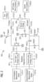
- FIG. 1 represents schematically an apparatus 5 that includes a fail-safe input-output (I/O) module circuit 7 and a diagnostic circuit 9 for detecting fault conditions in the energy supply of a load 10 in accordance with an exemplary embodiment of the present invention.
- I/O input-output
- the fail-safe input-output (I/O) module circuit 7 includes a first switch 12(1) coupled to a first resistor divider 15(1) and a first output 17(1) that supplies a DC supply voltage to the load 10 via a first wiring 20(1) to reduce a first voltage 22(1) of the first output 17(1) down to a first readback diagnostic output 25(1).
- the fail-safe input-output (I/O) module circuit 7 further includes a second switch 12(2) coupled to a second resistor divider 15(2) and a second output 17(2) that supplies the DC supply voltage to the load 10 via a second wiring 20(2) to reduce a second voltage 22(2) of the second output 17(2) down to a second readback diagnostic output 25(2).
- the diagnostic circuit 9 is coupled to the fail-safe input-output (I/O) module circuit 7.
- the diagnostic circuit 9 to provide a first readback measurement signal 27(1) from the first readback diagnostic output 25(1) and provide a second readback measurement signal 27(2) from the second readback diagnostic output 25(2).
- the apparatus 5 is configured to provide the first readback measurement signal 27(1) and the second readback measurement signal 27(2) for the first output 17(1) and the second output 17(2) with and without the load 10 such that when the first and second switches 12(1-2) are open or OFF the first voltage 22(1) at the first output 17(1) with the load 10 and the second voltage 22(2) at the second output 17(2) with the load 10 indicate a NOT broken wire condition 30(1) with respect to the first and second wirings 20(1-2) while the first voltage 22(1) at the first output 17(1) without the load 10 and the second voltage 22(2) at the second output 17(2) without the load 10 indicate a broken wire condition 30(2) with respect to the first and second wirings 20(1-2).
- the first output 17(1) and the second output 17(2) have the same voltage if the load 10 is connected or if the load 10 is not connected.
- the first output 17(1) and the second output 17(2) have a different voltage if the load 10 is connected or if the load 10 is not connected.
- the broken wire condition 30(2) or a missing load condition is discovered by examining voltage levels of the first output 17(1) and the second output 17(2) when both the first and second switches 12(1-2) are open or OFF.
- the thresholds for detecting a broken wire as a percentage of the DC supply voltage are used for the first output 17(1) and the second output 17(2) to determine whether there is the broken wire condition 30(2) or the missing load condition or there is a load connected condition.
- the first readback measurement signal 27(1) between a threshold1 and a threshold2 and the second readback measurement signal 27(2) between a threshold3 and a threshold4 indicates an output OFF condition or a load connected condition and wherein the first readback measurement signal 27(1) less than the threshold1 and the second readback measurement signal 27(2) between greater than the threshold4 indicates an output OFF condition or the broken wire condition 30(2).
- FIG. 2 it illustrates a circuit schematic of a PM output circuit 200 with a readback diagnostics circuit 202 in accordance with an exemplary embodiment of the present invention.
- the combination of the PM output circuit 200 and the readback diagnostics circuit 202 represents an apparatus for detecting fault conditions in the energy supply of a load 205.
- the PM output circuit 200 is a fail-safe input-output (I/O) module circuit that includes an input 207 for a DC supply voltage.
- the PM output circuit 200 further includes a first output 210(1) for supplying the DC supply voltage to a first terminal 212(1) of the load 205 via a first wiring 215(1).
- the PM output circuit 200 further includes a second output 210(2) for supplying the DC supply voltage to a second terminal 212(2) of the load 205 via a second wiring 215(2).
- the PM output circuit 200 further includes a first switch 217(1) coupled to a first resistor divider 220(1) and the first output 210(1) to reduce a first voltage 222(1) of the first output 210(1) down to a first readback diagnostic output 225(1).
- the PM output circuit 200 further includes a second switch 217(2) coupled to a second resistor divider 220(2) and the second output 210(2) to reduce a second voltage 222(2) of the second output 210(2) down to a second readback diagnostic output 225(2).
- the PM output circuit 200 further includes a resistor 230 and a diode 232 to bias the second output 210(2) when the second switch 217(2) if open or OFF.
- the readback diagnostics circuit 202 is a diagnostic circuit that is coupled to the PM output circuit 200 being the fail-safe input-output (I/O) module circuit.
- the readback diagnostics circuit 202 includes a first lower voltage circuit 235(1) coupled to the first readback diagnostic output 225(1) in series to provide a first readback measurement signal 237(1).
- the readback diagnostics circuit 202 further includes a second lower voltage circuit 235(2) coupled to the second readback diagnostic output 225(2) in series to provide a second readback measurement signal 237(2).
- the apparatus including the PM output circuit 200 and the readback diagnostics circuit 202 is configured to provide the first readback measurement signal 237(1) and the second readback measurement signal 237(2) for the first output 210(1) and the second output 210(2) with and without the load 205 such that when the first and second switches 217(1-2) are open or OFF the first voltage 222(1) at the first output 210(1) with the load 205 and the second voltage 222(2) at the second output 210(2) with the load 205 indicate a NOT broken wire condition 240(1) with respect to the first and second wirings 215(1-2) while the first voltage 222(1) at the first output 210(1) without the load 205 and the second voltage 222(2) at the second output 210(2) without the load 205 indicate a broken wire condition 240(2) with respect to the first and second wirings 215(1-2).
- Resistors R1 and R2 form a first resistor divider to reduce the voltage of the P-output down to P-Readback.
- P-Readback can be examined by lower voltage circuits.
- Resistors R4 and R5 form a second resistor divider to reduce the voltage of the M-output down to M-Readback.
- M-Readback can be examined by lower voltage circuits.
- Resistor R3 and Diode V1 bias the M-output when the M-switch is OFF. Suggested ratios for the resistors are following.
- R 1 + R 2 ⁇ R 3 .
- R 1 + R 2 > 10 * maximum Load resistance e.g., the Load may be an actuator or a motor
- the first output 210(1) and the second output 210(2) have the same voltage if the load 205 is connected or if the load 205 is not connected.
- the first switch 217(1) and the second switch 217(2) are both open or OFF, the first output 210(1) and the second output 210(2) have a different voltage if the load 205 is connected or if the load 205 is not connected.
- the broken wire condition 240(2) or a missing load condition is discovered by examining voltage levels of the first output 210(1) and the second output 210(2) when both the first and second switches 217(1-2) are open or OFF.
- the thresholds for detecting a broken wire as a percentage of the DC supply voltage are used for the first output 210(1) and the second output 210(2) to determine whether there is the broken wire condition 240(2) or the missing load condition or there is a load connected condition.
- the first readback measurement signal 237(1) between a threshold1 and a threshold2 and the second readback measurement signal 237(2) between a threshold3 and a threshold4 indicates an output OFF condition or a load connected condition.
- the first readback measurement signal 237(1) less than the threshold1 and the second readback measurement signal 237(2) between greater than the threshold4 indicates an output OFF condition or the broken wire condition 240(2).
- the DC supply voltage is 24V
- the threshold1 is 24% of 24V
- the threshold2 is 58% of 24V
- the threshold3 is 38% of 24V
- the threshold4 is 69% of 24V.
- the first readback measurement signal 237(1) and the second readback measurement signal 237(2) may be fed to an analog to digital converter (ADC) which is then read by a microprocessor to determine if criteria are met for the broken wire condition 240(2).
- ADC analog to digital converter
- first and second comparators may be used to check for the thresholds and then a state of the thresholds is interrogated by a microprocessor to see if criteria are met for the broken wire condition 240(2).
- a resistance of a resistor R4 245(1) in series with a resistor R5 245(2) is large in comparison to a resistance of the resistor R3 230 in parallel with the load 205.
- FIG. 3 it illustrates schematically an equivalent circuit 300 of a circuit in FIG. 2 including the PM output circuit 200 and the readback diagnostics circuit 202 being in a first combination of a P-Switch and a M-Switch as open or close in accordance with an exemplary embodiment of the present invention.
- the P-Switch and the M-Switch are both closed.
- a voltage for a M-output 305(1) may be "- VDD" and a voltage for a P-output 305(2) may be "-0V".
- FIG. 4 illustrates schematically an equivalent circuit 400 of a circuit in FIG. 2 including the PM output circuit 200 and the readback diagnostics circuit 202 being in a second combination of a P-Switch and a M-Switch as open or close in accordance with an exemplary embodiment of the present invention.
- the P-Switch is open and the M-Switch is closed.
- a voltage for a M-output 405(1) may be "- 0V" and a voltage for a P-output 405(2) may be "-0V".
- FIG. 5 it illustrates schematically an equivalent circuit 500 of a circuit in FIG. 2 including the PM output circuit 200 and the readback diagnostics circuit 202 being in a third combination of a P-Switch and a M-Switch as open or close in accordance with an exemplary embodiment of the present invention.
- the P-Switch is closed, and the M-Switch is open.
- a voltage for a M-output 505(1) may be " ⁇ VDD x (R4+R5) ⁇ / ⁇ (R4+R5) + (R3
- FIG. 6 it illustrates schematically an equivalent circuit 600 of a circuit in FIG. 2 including the PM output circuit 200 and the readback diagnostics circuit 202 being in a fourth combination of a P-Switch and a M-Switch as open or close in accordance with an exemplary embodiment of the present invention.
- the P-Switch and the M-Switch both are open.
- a voltage for a M-output 605(1) may be " ⁇ (VDD -VI) x [(R4+R5) ⁇ (Load + R1+R2)] ⁇ / ⁇ R3+[(R4+R5) ⁇ (Load+R1+R2)] ⁇ ” and a voltage for a P-output 605(2) may be " ⁇ M-output x (R1+R2) ⁇ / ⁇ Load+R1+R2 ⁇ ".
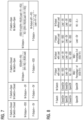
- FIG. 7 it shows equations for the voltage of a M-output and a P-output of the circuit in FIG. 2 as described in FIGs. 3-6 in accordance with an exemplary embodiment of the present invention.
- FIG. 8 shows a readback state of the expected readback signals for the P-output and the M-output with and without a load in accordance with an exemplary embodiment of the present invention.
- FIG. 8 shows the expected readback signals for the P-output and the M-output with and without a Load. This assumes that there has been enough time for the voltages to stabilize due to capacitive or inductive load effects. It also assumes that the resistance of R4 in series with R5 is large in comparison to the resistance of R3 in parallel with the Load.
- the P-output and the M-output have the same voltage if there is a Load connected or if there is no Load connected. Since the P-switch and M-switch voltages are different when both switches are OPEN, it is possible to determine when a Load is connected and when a Load is missing. As a result, a broken wire or missing Load can be discovered by examining the voltage levels of the P-output and the M-output switches when both switches are OFF.
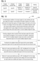
- FIG. 9 shows the thresholds used for the P-output and the M-output for detecting a broken wire of the PM output circuit 200 of FIG. 2 in accordance with an exemplary embodiment of the present invention.
- Threshold1 and Threshold2 are the extremes of Percentage1 when part tolerance, voltage variation, load variation and margin are considered.
- Threshold3 and Threshold4 are the extremes of Percentage2 when part tolerance, voltage variation, load variation and margin are considered.
- ADC analog to digital converter
- Another method is to use comparators to check for the thresholds. Then the state of the thresholds could be interrogated by a microprocessor to see if the conditions are met for a broken wire.
- FIG. 10 illustrates a flow chart of a method 1000 of detecting fault conditions in the energy supply of a load according to one exemplary embodiment of the present invention. Reference is made to the elements and features described in FIGs. 1-9 . It should be appreciated that some steps are not required to be performed in any particular order, and that some steps are optional.
- the method 1000 includes a step 1005 of providing a fail-safe input-output (I/O) module circuit.
- This circuit includes a first switch coupled to a first resistor divider and a first output that supplies a DC supply voltage to the load via a first wiring to reduce a first voltage of the first output down to a first readback diagnostic output and a second switch coupled to a second resistor divider and a second output that supplies the DC supply voltage to the load via a second wiring to reduce a second voltage of the second output down to a second readback diagnostic output.
- I/O input-output
- the method 1000 further includes a step 1010 of providing a diagnostic circuit coupled to the fail-safe input-output (I/O) module circuit.
- the diagnostic circuit to provide a first readback measurement signal from the first readback diagnostic output and provide a second readback measurement signal from the second readback diagnostic output.
- the method 1000 further includes a step 1015 providing the first readback measurement signal and the second readback measurement signal for the first output and the second output with and without the load.
- the method 1000 further includes a step 1020 of indicating with the first voltage at the first output with the load and the second voltage at the second output with the load a NOT broken wire condition with respect to the first and second wirings.
- the method 1000 further includes a step 1025 of indicating with the first voltage at the first output without the load and the second voltage at the second output without the load a broken wire condition with respect to the first and second wirings.
- the method 1000 includes in all cases except when the first switch and second switch are both open or OFF, the first output and the second output have the same voltage if the load is connected or if the load is not connected.
- the method 1000 includes when the first switch and second switch are both open or OFF, the first output and the second output have a different voltage if the load is connected or if the load is not connected.
- the techniques described herein can be particularly useful for fault detection in the power supply to a load in terms of broken wire detection for a functional safety DC output on an industrial control. While particular embodiments are described in terms of such an industrial control, the fault detection techniques described herein are not limited to the industrial control but can also be used with other suitable applications.
Landscapes
- Physics & Mathematics (AREA)
- General Physics & Mathematics (AREA)
- Engineering & Computer Science (AREA)
- Automation & Control Theory (AREA)
- Testing Of Short-Circuits, Discontinuities, Leakage, Or Incorrect Line Connections (AREA)
Claims (8)
- Einrichtung (5) zum Detektieren von Fehlerbedingungen bei der Energieversorgung einer Last (10, 205), wobei die Einrichtung (5) Folgendes umfasst:
eine Fail-Safe-Eingabe-Ausgabe-Modulschaltung (7, 200), die Folgendes beinhaltet:einen Eingang (207) für eine DC-Versorgungsspannung;einen ersten Ausgang (210(1)) zum Zuführen der DC-Versorgungsspannung zu einem ersten Anschluss (212(1)) der Last (10, 205) über eine erste Verdrahtung (215(1));einen zweiten Ausgang (210(2)) zum Zuführen der DC-Versorgungsspannung zu einem zweiten Anschluss (212(2)) der Last (10, 205) über eine zweite Verdrahtung (215(2));einen ersten Widerstandsteiler (220(1)) mit einem ersten Widerstand (R1) und einem zweiten Widerstand (R2);einen ersten Schalter (217(1)), der mit dem ersten Widerstandsteiler (220(1)) und dem ersten Ausgang (210(1)) gekoppelt ist, um eine erste Spannung (222(1)) des ersten Ausgangs (210(1)) auf eine erste Rücklesediagnoseausgabe (225(1)) zu reduzieren;einen zweiten Widerstandsteiler (220(2)) mit einem vierten Widerstand (R4) und einem fünften Widerstand (R5);einen zweiten Schalter (217(2)), der mit dem zweiten Widerstandsteiler (220(2)) und dem zweiten Ausgang (210(2)) gekoppelt ist, um eine zweite Spannung (222(2)) des zweiten Ausgangs (210(2)) auf eine zweite Rücklesediagnoseausgabe (235(2)) zu reduzieren;einen dritten Widerstand (R3) und eine Diode (V1) zum Vorspannen des zweiten Ausgangs (210(2)), wenn der zweite Schalter (217(2)) offen oder AUS ist; undeine Diagnoseschaltung (9, 202), die mit der Fail-Safe-Eingabe/Ausgabe-Modulschaltung (7, 200) gekoppelt ist, wobei die Diagnoseschaltung (9, 202) Folgendes beinhaltet:eine erste Schaltung (235(1)) für niedrigere Spannung, die mit dem ersten Rücklesediagnoseausgang (225(1)) in Reihe geschaltet ist, um ein erstes Rücklesemesssignal (237(1)) bereitzustellen;eine zweite Schaltung (235(2)) für niedrigere Spannung, die mit dem zweiten Rücklesediagnoseausgang (225(2)) in Reihe geschaltet ist, um ein zweites Rücklesemesssignal (237(2)) bereitzustellen, wobei die Einrichtung (5) dazu ausgelegt ist, das erste Rücklesemesssignal (237(1)) und das zweite Rücklesemesssignal (237(2)) für den ersten Ausgang (210(1)) und den zweiten Ausgang (210(2)) mit und ohne die Last (10, 205) bereitzustellen,wobei die Einrichtung (5) dazu ausgelegt ist, das erste Rücklesemesssignal (237(1)) und das zweite Rücklesemesssignal (237(2)) derart bereitzustellen, dass, wenn der erste und der zweite Schalter (217(1), 217(2)) offen oder AUS sind, die erste Spannung (222(1)) am ersten Ausgang (210(1)) mit der Last (10, 205) und die zweite Spannung (222(2)) am zweiten Ausgang (210(2)) mit der Last (10, 205) einen Draht-NICHT-unterbrochen-Zustand (240(1)) mit Bezug auf die erste und die zweite Verdrahtungen (215(1), 215(2)) angeben, während die erste Spannung (222(1)) am ersten Ausgang (210(1)) ohne die Last (10, 205) und die zweite Spannung (222(2)) am zweiten Ausgang (210(2)) ohne die Last (10, 205) einen Draht-unterbrochen-Zustand (240(2)) in Bezug auf die erste und die zweite Verdrahtung (215(1), 215(2)) angeben, undwobei die Einrichtung (5) dazu ausgelegt ist, einen Ausgang-AUS-Zustand oder einen Last(10, 205)-verbunden-Zustand zu identifizieren, wenn das erste Rücklesemesssignal (237(1)) zwischen einer ersten Schwelle und einer zweiten Schwelle liegt und das zweite Rücklesemesssignal (237(2)) zwischen einer dritten Schwelle und einer vierten Schwelle liegt. - Einrichtung (5) nach Anspruch 1, wobei die Einrichtung (5) dazu ausgelegt ist, einen Ausgang-AUS-Zustand oder einen Draht-unterbrochen-Zustand zu identifizieren, wenn das erste Rücklesemesssignal (237(1)) kleiner als die erste Schwelle ist und das zweite Rücklesemesssignal (237(2)) größer als die vierte Schwelle ist.
- Einrichtung (5) nach Anspruch 1 oder 2, wobei der Ausgang-AUS-Zustand, der Last(10, 205)-verbunden-Zustand und/oder der Draht-unterbrochen-Zustand durch Prüfen von Spannungspegeln des ersten Ausgangs (210(1)) und des zweiten Ausgangs (210(2)) festgestellt werden, wenn sowohl der erste als auch der zweite Schalter (217(1), 217(2)) offen oder AUS sind.
- Einrichtung (5) nach einem der vorhergehenden Ansprüche, wobei Schwellen zum Detektieren eines unterbrochenen Drahts als Prozentsatz der DC-Versorgungsspannung für den ersten Ausgang (210(1)) und den zweiten Ausgang (210(2)) verwendet werden, um zu bestimmen, ob der Draht-unterbrochen-Zustand oder der Fehlende-Last(10, 205)-Zustand vorliegt oder ein Last(10, 205)-verbunden-Zustand vorliegt.
- Einrichtung (5) nach Anspruch 2, wobei die DC-Versorgungsspannung 24 V beträgt, die erste Schwelle 24 % von 24 V beträgt, die zweite Schwelle 58 % von 24 V beträgt, die dritte Schwelle 38 % von 24 V beträgt und die vierte Schwelle 69 % von 24 V beträgt.
- Einrichtung (5) nach einem der vorhergehenden Ansprüche, wobei das erste Rücklesemesssignal (237(1)) und das zweite Rücklesemesssignal (237(2)) einem Analog-Digital-Wandler zugeführt werden, der dann von einem Mikroprozessor gelesen wird, um zu bestimmen, ob Kriterien für den Draht-unterbrochen-Zustand erfüllt sind.
- Einrichtung (5) nach einem der Ansprüche 1-5, wobei erste und zweite Komparatoren verwendet werden, um auf die Schwellen zu prüfen, und dann ein Zustand der Schwellen durch einen Mikroprozessor abgefragt wird, um festzustellen, ob Kriterien für den Draht-unterbrochen-Zustand erfüllt sind.
- Einrichtung (5) nach einem der vorhergehenden Ansprüche, wobei ein Widerstandswert des vierten Widerstands (R4) in Reihenschaltung mit dem fünften Widerstand (R5) im Vergleich zu einem Widerstandswert des dritten Widerstands (R3) in Parallelschaltung mit der Last (10, 205) groß ist.
Applications Claiming Priority (1)
| Application Number | Priority Date | Filing Date | Title |
|---|---|---|---|
| PCT/US2018/034609 WO2019226171A1 (en) | 2018-05-25 | 2018-05-25 | Fault detection in power supply to a load in terms of a broken wire detection for a functional safety dc output |
Publications (3)
| Publication Number | Publication Date |
|---|---|
| EP3775945A1 EP3775945A1 (de) | 2021-02-17 |
| EP3775945C0 EP3775945C0 (de) | 2025-06-25 |
| EP3775945B1 true EP3775945B1 (de) | 2025-06-25 |
Family
ID=62837972
Family Applications (1)
| Application Number | Title | Priority Date | Filing Date |
|---|---|---|---|
| EP18737739.5A Active EP3775945B1 (de) | 2018-05-25 | 2018-05-25 | Fehlererkennung in der stromversorgung einer last hinsichtlich einer drahtrisserkennung für einen funktionssicheren gleichspannungsausgang |
Country Status (4)
| Country | Link |
|---|---|
| US (1) | US11675327B2 (de) |
| EP (1) | EP3775945B1 (de) |
| CN (1) | CN112189144B (de) |
| WO (1) | WO2019226171A1 (de) |
Families Citing this family (3)
| Publication number | Priority date | Publication date | Assignee | Title |
|---|---|---|---|---|
| EP4137822B1 (de) * | 2021-08-17 | 2024-04-17 | Siemens Aktiengesellschaft | Verfahren zur erhöhung einer ausfallsicherheit einer industriellen ein-/ausgabebaugruppe und eine ein-/ausgabebaugruppe |
| CN114779125B (zh) * | 2022-04-24 | 2024-12-20 | 南京科远智慧科技集团股份有限公司 | 一种数字量输出回路断线诊断装置及诊断方法 |
| CN116626528A (zh) * | 2023-05-18 | 2023-08-22 | 广州明美新能源股份有限公司 | 一种负载检测电路和负载检测方法 |
Family Cites Families (13)
| Publication number | Priority date | Publication date | Assignee | Title |
|---|---|---|---|---|
| DE19516208C1 (de) * | 1995-05-03 | 1996-07-25 | Siemens Ag | Verfahren zur Überwachung einer Leistungsendstufe und Schaltungsanordnung zur Durchführung dieses Verfahrens |
| DE19723456C2 (de) * | 1997-06-04 | 2003-03-27 | Siemens Ag | Fehlschlußerkennungseinrichtung für elektrische Verbraucher |
| WO2001094959A2 (en) | 2000-06-02 | 2001-12-13 | Siemens Automotive Corporation | System and method for diagnosing fault conditions associated with powering an electrical load |
| WO2009115869A1 (en) * | 2008-03-20 | 2009-09-24 | Freescale Semiconductor, Inc. | Apparatus and a method for detecting faults in the delivery of electrical power to electrical loads |
| PL2796887T3 (pl) * | 2012-03-27 | 2020-05-18 | Lg Chem, Ltd. | Aparat do pomiaru rezystancji izolacji, mający funkcję autodiagnozowania usterek, oraz sposób autodiagnozowania usterek przy jego użyciu |
| DE102012212123B4 (de) * | 2012-07-11 | 2016-05-19 | Continental Automotive Gmbh | Vorrichtung zur Diagnose einer Schaltungsanordnung |
| JP6375908B2 (ja) * | 2014-12-03 | 2018-08-22 | 株式会社デンソー | Dc−dcコンバータの制御装置 |
| US10426342B2 (en) * | 2016-03-31 | 2019-10-01 | Zoll Medical Corporation | Remote access for ambulatory medical device |
| US10340908B2 (en) | 2016-07-25 | 2019-07-02 | Continental Automotive Systems, Inc. | Half-bridge driver fault diagnostic system and method |
| US10967147B2 (en) * | 2018-06-28 | 2021-04-06 | St. Jude Medical International Holding S.À R.L. | Reliability determination of electrode location data |
| US10983103B2 (en) * | 2018-11-23 | 2021-04-20 | Msa Technology, Llc | Detection of blockage in a porous member |
| US11135429B2 (en) * | 2019-04-26 | 2021-10-05 | Medtronic, Inc. | Neural oscillatory signal source location detection |
| DE102019121794A1 (de) * | 2019-08-13 | 2021-02-18 | Infineon Technologies Ag | Intelligenter elektronischer schalter |
-
2018
- 2018-05-25 US US17/051,020 patent/US11675327B2/en active Active
- 2018-05-25 CN CN201880093734.5A patent/CN112189144B/zh active Active
- 2018-05-25 EP EP18737739.5A patent/EP3775945B1/de active Active
- 2018-05-25 WO PCT/US2018/034609 patent/WO2019226171A1/en not_active Ceased
Also Published As
| Publication number | Publication date |
|---|---|
| CN112189144A (zh) | 2021-01-05 |
| EP3775945C0 (de) | 2025-06-25 |
| EP3775945A1 (de) | 2021-02-17 |
| US11675327B2 (en) | 2023-06-13 |
| CN112189144B (zh) | 2023-09-29 |
| WO2019226171A1 (en) | 2019-11-28 |
| US20210123983A1 (en) | 2021-04-29 |
Similar Documents
| Publication | Publication Date | Title |
|---|---|---|
| US11431162B2 (en) | Smart electronic switch | |
| US7772725B2 (en) | Apparatus and method for current control in H-Bridge load drivers | |
| KR102155973B1 (ko) | 하프-브릿지 드라이버 결함 진단 시스템 및 방법 | |
| CN105846803B (zh) | 包括电子流检测块的固态继电器 | |
| CN102822930B (zh) | 用于电气电路监控的装置、用于为负载供电的电路装置和用于运行电路装置的方法 | |
| US9550423B2 (en) | Interlock switching circuit for protecting an electrical on-board power supply | |
| CN108068729B (zh) | 包括具有同时开关状态检测功能的多重模拟开关监测系统的车辆 | |
| CN114987202A (zh) | 使电流流动中断的接触器、集成电路、方法 | |
| EP3775945B1 (de) | Fehlererkennung in der stromversorgung einer last hinsichtlich einer drahtrisserkennung für einen funktionssicheren gleichspannungsausgang | |
| US20140333320A1 (en) | Circuit arrangement for detecting a short circuit in a power switch arrangement | |
| CN104583787A (zh) | 用于诊断电路装置的设备 | |
| CN110658481A (zh) | 接地丢失检测系统 | |
| US10740272B2 (en) | Input circuit that can be made redundant, input circuit unit having at least one input circuit, and method for operating the input circuit unit | |
| US20010048367A1 (en) | System and method for diagnosing fault conditions associated with powering an electrical load | |
| US11124138B2 (en) | Device for supplying power to a control unit and method for monitoring a power supply | |
| CN101836355A (zh) | 用于识别负载降低的方法 | |
| US20190308572A1 (en) | Multi-voltage control device for a motor vehicle, motor vehicle and operating method for the control device | |
| CN113841313B (zh) | 用于致动器的电流控制的设备和方法 | |
| EP1974247B1 (de) | Erfassen eines betriebszustands eines systems | |
| US10848157B2 (en) | Level converter and a method for converting level values in vehicle control devices | |
| US6960915B2 (en) | Electric circuit system | |
| CN113985147A (zh) | 车辆的地偏移检测装置及方法 | |
| EP0995997A1 (de) | Fehlererkennungsvorrichtung eines elektromagnetischen gesteverten anordnung | |
| KR100738450B1 (ko) | 스위칭 소자의 병렬 구동회로 | |
| JP2020141230A (ja) | スイッチの状態診断回路及びそれを用いた負荷制御装置 |
Legal Events
| Date | Code | Title | Description |
|---|---|---|---|
| STAA | Information on the status of an ep patent application or granted ep patent |
Free format text: STATUS: UNKNOWN |
|
| STAA | Information on the status of an ep patent application or granted ep patent |
Free format text: STATUS: THE INTERNATIONAL PUBLICATION HAS BEEN MADE |
|
| PUAI | Public reference made under article 153(3) epc to a published international application that has entered the european phase |
Free format text: ORIGINAL CODE: 0009012 |
|
| STAA | Information on the status of an ep patent application or granted ep patent |
Free format text: STATUS: REQUEST FOR EXAMINATION WAS MADE |
|
| 17P | Request for examination filed |
Effective date: 20201027 |
|
| AK | Designated contracting states |
Kind code of ref document: A1 Designated state(s): AL AT BE BG CH CY CZ DE DK EE ES FI FR GB GR HR HU IE IS IT LI LT LU LV MC MK MT NL NO PL PT RO RS SE SI SK SM TR |
|
| AX | Request for extension of the european patent |
Extension state: BA ME |
|
| DAV | Request for validation of the european patent (deleted) | ||
| DAX | Request for extension of the european patent (deleted) | ||
| RAP1 | Party data changed (applicant data changed or rights of an application transferred) |
Owner name: SIEMENS AKTIENGESELLSCHAFT |
|
| STAA | Information on the status of an ep patent application or granted ep patent |
Free format text: STATUS: EXAMINATION IS IN PROGRESS |
|
| 17Q | First examination report despatched |
Effective date: 20220817 |
|
| REG | Reference to a national code |
Ref country code: DE Ref legal event code: R079 Free format text: PREVIOUS MAIN CLASS: G01R0031020000 Ipc: G05B0019050000 Ref country code: DE Ref legal event code: R079 Ref document number: 602018082903 Country of ref document: DE Free format text: PREVIOUS MAIN CLASS: G01R0031020000 Ipc: G05B0019050000 |
|
| RIC1 | Information provided on ipc code assigned before grant |
Ipc: G01R 31/58 20200101ALI20230331BHEP Ipc: G01R 31/54 20200101ALI20230331BHEP Ipc: G01R 31/40 20200101ALI20230331BHEP Ipc: G05B 19/05 20060101AFI20230331BHEP |
|
| GRAP | Despatch of communication of intention to grant a patent |
Free format text: ORIGINAL CODE: EPIDOSNIGR1 |
|
| STAA | Information on the status of an ep patent application or granted ep patent |
Free format text: STATUS: GRANT OF PATENT IS INTENDED |
|
| INTG | Intention to grant announced |
Effective date: 20230602 |
|
| GRAJ | Information related to disapproval of communication of intention to grant by the applicant or resumption of examination proceedings by the epo deleted |
Free format text: ORIGINAL CODE: EPIDOSDIGR1 |
|
| STAA | Information on the status of an ep patent application or granted ep patent |
Free format text: STATUS: EXAMINATION IS IN PROGRESS |
|
| INTC | Intention to grant announced (deleted) | ||
| GRAP | Despatch of communication of intention to grant a patent |
Free format text: ORIGINAL CODE: EPIDOSNIGR1 |
|
| STAA | Information on the status of an ep patent application or granted ep patent |
Free format text: STATUS: GRANT OF PATENT IS INTENDED |
|
| INTG | Intention to grant announced |
Effective date: 20250121 |
|
| GRAS | Grant fee paid |
Free format text: ORIGINAL CODE: EPIDOSNIGR3 |
|
| GRAA | (expected) grant |
Free format text: ORIGINAL CODE: 0009210 |
|
| STAA | Information on the status of an ep patent application or granted ep patent |
Free format text: STATUS: THE PATENT HAS BEEN GRANTED |
|
| AK | Designated contracting states |
Kind code of ref document: B1 Designated state(s): AL AT BE BG CH CY CZ DE DK EE ES FI FR GB GR HR HU IE IS IT LI LT LU LV MC MK MT NL NO PL PT RO RS SE SI SK SM TR |
|
| REG | Reference to a national code |
Ref country code: GB Ref legal event code: FG4D |
|
| REG | Reference to a national code |
Ref country code: CH Ref legal event code: EP |
|
| REG | Reference to a national code |
Ref country code: DE Ref legal event code: R096 Ref document number: 602018082903 Country of ref document: DE |
|
| REG | Reference to a national code |
Ref country code: CH Ref legal event code: EP |
|
| REG | Reference to a national code |
Ref country code: IE Ref legal event code: FG4D |
|
| U01 | Request for unitary effect filed |
Effective date: 20250625 |
|
| U07 | Unitary effect registered |
Designated state(s): AT BE BG DE DK EE FI FR IT LT LU LV MT NL PT RO SE SI Effective date: 20250701 |
|
| PG25 | Lapsed in a contracting state [announced via postgrant information from national office to epo] |
Ref country code: NO Free format text: LAPSE BECAUSE OF FAILURE TO SUBMIT A TRANSLATION OF THE DESCRIPTION OR TO PAY THE FEE WITHIN THE PRESCRIBED TIME-LIMIT Effective date: 20250925 Ref country code: GR Free format text: LAPSE BECAUSE OF FAILURE TO SUBMIT A TRANSLATION OF THE DESCRIPTION OR TO PAY THE FEE WITHIN THE PRESCRIBED TIME-LIMIT Effective date: 20250926 |
|
| PG25 | Lapsed in a contracting state [announced via postgrant information from national office to epo] |
Ref country code: HR Free format text: LAPSE BECAUSE OF FAILURE TO SUBMIT A TRANSLATION OF THE DESCRIPTION OR TO PAY THE FEE WITHIN THE PRESCRIBED TIME-LIMIT Effective date: 20250625 |
|
| PG25 | Lapsed in a contracting state [announced via postgrant information from national office to epo] |
Ref country code: RS Free format text: LAPSE BECAUSE OF FAILURE TO SUBMIT A TRANSLATION OF THE DESCRIPTION OR TO PAY THE FEE WITHIN THE PRESCRIBED TIME-LIMIT Effective date: 20250925 |
|
| PG25 | Lapsed in a contracting state [announced via postgrant information from national office to epo] |
Ref country code: IS Free format text: LAPSE BECAUSE OF FAILURE TO SUBMIT A TRANSLATION OF THE DESCRIPTION OR TO PAY THE FEE WITHIN THE PRESCRIBED TIME-LIMIT Effective date: 20251025 |
|
| PG25 | Lapsed in a contracting state [announced via postgrant information from national office to epo] |
Ref country code: SM Free format text: LAPSE BECAUSE OF FAILURE TO SUBMIT A TRANSLATION OF THE DESCRIPTION OR TO PAY THE FEE WITHIN THE PRESCRIBED TIME-LIMIT Effective date: 20250625 |
|
| PG25 | Lapsed in a contracting state [announced via postgrant information from national office to epo] |
Ref country code: CZ Free format text: LAPSE BECAUSE OF FAILURE TO SUBMIT A TRANSLATION OF THE DESCRIPTION OR TO PAY THE FEE WITHIN THE PRESCRIBED TIME-LIMIT Effective date: 20250625 |
|
| PG25 | Lapsed in a contracting state [announced via postgrant information from national office to epo] |
Ref country code: PL Free format text: LAPSE BECAUSE OF FAILURE TO SUBMIT A TRANSLATION OF THE DESCRIPTION OR TO PAY THE FEE WITHIN THE PRESCRIBED TIME-LIMIT Effective date: 20250625 |
|
| PG25 | Lapsed in a contracting state [announced via postgrant information from national office to epo] |
Ref country code: SK Free format text: LAPSE BECAUSE OF FAILURE TO SUBMIT A TRANSLATION OF THE DESCRIPTION OR TO PAY THE FEE WITHIN THE PRESCRIBED TIME-LIMIT Effective date: 20250625 |
|
| PG25 | Lapsed in a contracting state [announced via postgrant information from national office to epo] |
Ref country code: ES Free format text: LAPSE BECAUSE OF FAILURE TO SUBMIT A TRANSLATION OF THE DESCRIPTION OR TO PAY THE FEE WITHIN THE PRESCRIBED TIME-LIMIT Effective date: 20250625 |
|
| PLBE | No opposition filed within time limit |
Free format text: ORIGINAL CODE: 0009261 |
|
| STAA | Information on the status of an ep patent application or granted ep patent |
Free format text: STATUS: NO OPPOSITION FILED WITHIN TIME LIMIT |