EP3772121B1 - Electricity supply system and package structure thereof - Google Patents
Electricity supply system and package structure thereof Download PDFInfo
- Publication number
- EP3772121B1 EP3772121B1 EP19203124.3A EP19203124A EP3772121B1 EP 3772121 B1 EP3772121 B1 EP 3772121B1 EP 19203124 A EP19203124 A EP 19203124A EP 3772121 B1 EP3772121 B1 EP 3772121B1
- Authority
- EP
- European Patent Office
- Prior art keywords
- silicone
- layer
- electricity supply
- active material
- supply system
- Prior art date
- Legal status (The legal status is an assumption and is not a legal conclusion. Google has not performed a legal analysis and makes no representation as to the accuracy of the status listed.)
- Active
Links
- 230000005611 electricity Effects 0.000 title claims description 98
- 229920001296 polysiloxane Polymers 0.000 claims description 125
- 238000007789 sealing Methods 0.000 claims description 63
- 239000011149 active material Substances 0.000 claims description 56
- 239000000126 substance Substances 0.000 claims description 25
- 229910052751 metal Inorganic materials 0.000 claims description 15
- 239000002184 metal Substances 0.000 claims description 15
- VYPSYNLAJGMNEJ-UHFFFAOYSA-N Silicium dioxide Chemical compound O=[Si]=O VYPSYNLAJGMNEJ-UHFFFAOYSA-N 0.000 claims description 4
- 239000002245 particle Substances 0.000 claims description 4
- 125000006850 spacer group Chemical group 0.000 claims description 4
- SMZOUWXMTYCWNB-UHFFFAOYSA-N 2-(2-methoxy-5-methylphenyl)ethanamine Chemical compound COC1=CC=C(C)C=C1CCN SMZOUWXMTYCWNB-UHFFFAOYSA-N 0.000 claims description 2
- NIXOWILDQLNWCW-UHFFFAOYSA-N 2-Propenoic acid Natural products OC(=O)C=C NIXOWILDQLNWCW-UHFFFAOYSA-N 0.000 claims description 2
- 239000004593 Epoxy Substances 0.000 claims description 2
- GWEVSGVZZGPLCZ-UHFFFAOYSA-N Titan oxide Chemical compound O=[Ti]=O GWEVSGVZZGPLCZ-UHFFFAOYSA-N 0.000 claims description 2
- 235000012239 silicon dioxide Nutrition 0.000 claims description 2
- 239000000377 silicon dioxide Substances 0.000 claims description 2
- OGIDPMRJRNCKJF-UHFFFAOYSA-N titanium oxide Inorganic materials [Ti]=O OGIDPMRJRNCKJF-UHFFFAOYSA-N 0.000 claims description 2
- 239000006183 anode active material Substances 0.000 claims 1
- 239000006182 cathode active material Substances 0.000 claims 1
- 239000010410 layer Substances 0.000 description 224
- 239000000758 substrate Substances 0.000 description 125
- 229910052744 lithium Inorganic materials 0.000 description 28
- WHXSMMKQMYFTQS-UHFFFAOYSA-N Lithium Chemical compound [Li] WHXSMMKQMYFTQS-UHFFFAOYSA-N 0.000 description 26
- 239000000463 material Substances 0.000 description 19
- 238000000034 method Methods 0.000 description 16
- 239000003792 electrolyte Substances 0.000 description 11
- 239000007789 gas Substances 0.000 description 11
- 238000010438 heat treatment Methods 0.000 description 8
- 229920000642 polymer Polymers 0.000 description 8
- 230000008569 process Effects 0.000 description 8
- 238000013461 design Methods 0.000 description 7
- 230000002829 reductive effect Effects 0.000 description 7
- 238000012360 testing method Methods 0.000 description 7
- 238000006243 chemical reaction Methods 0.000 description 5
- 230000002093 peripheral effect Effects 0.000 description 5
- 230000032683 aging Effects 0.000 description 4
- 238000004804 winding Methods 0.000 description 4
- HBBGRARXTFLTSG-UHFFFAOYSA-N Lithium ion Chemical compound [Li+] HBBGRARXTFLTSG-UHFFFAOYSA-N 0.000 description 3
- 230000015572 biosynthetic process Effects 0.000 description 3
- 238000001723 curing Methods 0.000 description 3
- 229910001416 lithium ion Inorganic materials 0.000 description 3
- 238000004519 manufacturing process Methods 0.000 description 3
- 238000006116 polymerization reaction Methods 0.000 description 3
- PXHVJJICTQNCMI-UHFFFAOYSA-N Nickel Chemical compound [Ni] PXHVJJICTQNCMI-UHFFFAOYSA-N 0.000 description 2
- QVGXLLKOCUKJST-UHFFFAOYSA-N atomic oxygen Chemical compound [O] QVGXLLKOCUKJST-UHFFFAOYSA-N 0.000 description 2
- 230000004888 barrier function Effects 0.000 description 2
- 238000000576 coating method Methods 0.000 description 2
- 239000002131 composite material Substances 0.000 description 2
- 238000004880 explosion Methods 0.000 description 2
- 230000002209 hydrophobic effect Effects 0.000 description 2
- 150000002500 ions Chemical class 0.000 description 2
- 230000005012 migration Effects 0.000 description 2
- 238000013508 migration Methods 0.000 description 2
- 238000012986 modification Methods 0.000 description 2
- 230000004048 modification Effects 0.000 description 2
- 239000001301 oxygen Substances 0.000 description 2
- 229910052760 oxygen Inorganic materials 0.000 description 2
- 230000036961 partial effect Effects 0.000 description 2
- 230000035515 penetration Effects 0.000 description 2
- 238000003825 pressing Methods 0.000 description 2
- 238000007650 screen-printing Methods 0.000 description 2
- 239000007787 solid Substances 0.000 description 2
- 230000035882 stress Effects 0.000 description 2
- XLYOFNOQVPJJNP-UHFFFAOYSA-N water Chemical compound O XLYOFNOQVPJJNP-UHFFFAOYSA-N 0.000 description 2
- RYGMFSIKBFXOCR-UHFFFAOYSA-N Copper Chemical compound [Cu] RYGMFSIKBFXOCR-UHFFFAOYSA-N 0.000 description 1
- 239000000654 additive Substances 0.000 description 1
- 239000012790 adhesive layer Substances 0.000 description 1
- 239000000919 ceramic Substances 0.000 description 1
- 239000011248 coating agent Substances 0.000 description 1
- 238000004891 communication Methods 0.000 description 1
- 229910052802 copper Inorganic materials 0.000 description 1
- 239000010949 copper Substances 0.000 description 1
- 238000011161 development Methods 0.000 description 1
- 230000018109 developmental process Effects 0.000 description 1
- 238000007599 discharging Methods 0.000 description 1
- 230000000694 effects Effects 0.000 description 1
- 238000003487 electrochemical reaction Methods 0.000 description 1
- 230000007613 environmental effect Effects 0.000 description 1
- 230000003628 erosive effect Effects 0.000 description 1
- 238000010304 firing Methods 0.000 description 1
- 239000000446 fuel Substances 0.000 description 1
- 239000011521 glass Substances 0.000 description 1
- 239000003365 glass fiber Substances 0.000 description 1
- 230000009477 glass transition Effects 0.000 description 1
- 239000003292 glue Substances 0.000 description 1
- 238000007731 hot pressing Methods 0.000 description 1
- 230000003116 impacting effect Effects 0.000 description 1
- 230000002147 killing effect Effects 0.000 description 1
- 239000007791 liquid phase Substances 0.000 description 1
- 239000007769 metal material Substances 0.000 description 1
- 229910052759 nickel Inorganic materials 0.000 description 1
- 230000000149 penetrating effect Effects 0.000 description 1
- 239000004033 plastic Substances 0.000 description 1
- 239000004014 plasticizer Substances 0.000 description 1
- 239000002798 polar solvent Substances 0.000 description 1
- 230000004224 protection Effects 0.000 description 1
- 230000001681 protective effect Effects 0.000 description 1
- 239000007790 solid phase Substances 0.000 description 1
- 238000010186 staining Methods 0.000 description 1
- 238000001029 thermal curing Methods 0.000 description 1
- 238000007669 thermal treatment Methods 0.000 description 1
- 238000003466 welding Methods 0.000 description 1
Images


Classifications
-
- H—ELECTRICITY
- H01—ELECTRIC ELEMENTS
- H01M—PROCESSES OR MEANS, e.g. BATTERIES, FOR THE DIRECT CONVERSION OF CHEMICAL ENERGY INTO ELECTRICAL ENERGY
- H01M50/00—Constructional details or processes of manufacture of the non-active parts of electrochemical cells other than fuel cells, e.g. hybrid cells
- H01M50/10—Primary casings, jackets or wrappings of a single cell or a single battery
- H01M50/183—Sealing members
- H01M50/184—Sealing members characterised by their shape or structure
-
- H—ELECTRICITY
- H01—ELECTRIC ELEMENTS
- H01M—PROCESSES OR MEANS, e.g. BATTERIES, FOR THE DIRECT CONVERSION OF CHEMICAL ENERGY INTO ELECTRICAL ENERGY
- H01M50/00—Constructional details or processes of manufacture of the non-active parts of electrochemical cells other than fuel cells, e.g. hybrid cells
- H01M50/10—Primary casings, jackets or wrappings of a single cell or a single battery
- H01M50/172—Arrangements of electric connectors penetrating the casing
- H01M50/174—Arrangements of electric connectors penetrating the casing adapted for the shape of the cells
- H01M50/176—Arrangements of electric connectors penetrating the casing adapted for the shape of the cells for prismatic or rectangular cells
-
- H—ELECTRICITY
- H01—ELECTRIC ELEMENTS
- H01M—PROCESSES OR MEANS, e.g. BATTERIES, FOR THE DIRECT CONVERSION OF CHEMICAL ENERGY INTO ELECTRICAL ENERGY
- H01M10/00—Secondary cells; Manufacture thereof
- H01M10/05—Accumulators with non-aqueous electrolyte
- H01M10/052—Li-accumulators
-
- H—ELECTRICITY
- H01—ELECTRIC ELEMENTS
- H01M—PROCESSES OR MEANS, e.g. BATTERIES, FOR THE DIRECT CONVERSION OF CHEMICAL ENERGY INTO ELECTRICAL ENERGY
- H01M50/00—Constructional details or processes of manufacture of the non-active parts of electrochemical cells other than fuel cells, e.g. hybrid cells
- H01M50/10—Primary casings, jackets or wrappings of a single cell or a single battery
- H01M50/183—Sealing members
- H01M50/19—Sealing members characterised by the material
- H01M50/197—Sealing members characterised by the material having a layered structure
-
- H—ELECTRICITY
- H01—ELECTRIC ELEMENTS
- H01M—PROCESSES OR MEANS, e.g. BATTERIES, FOR THE DIRECT CONVERSION OF CHEMICAL ENERGY INTO ELECTRICAL ENERGY
- H01M10/00—Secondary cells; Manufacture thereof
- H01M10/42—Methods or arrangements for servicing or maintenance of secondary cells or secondary half-cells
-
- H—ELECTRICITY
- H01—ELECTRIC ELEMENTS
- H01M—PROCESSES OR MEANS, e.g. BATTERIES, FOR THE DIRECT CONVERSION OF CHEMICAL ENERGY INTO ELECTRICAL ENERGY
- H01M50/00—Constructional details or processes of manufacture of the non-active parts of electrochemical cells other than fuel cells, e.g. hybrid cells
- H01M50/10—Primary casings, jackets or wrappings of a single cell or a single battery
- H01M50/172—Arrangements of electric connectors penetrating the casing
- H01M50/174—Arrangements of electric connectors penetrating the casing adapted for the shape of the cells
- H01M50/179—Arrangements of electric connectors penetrating the casing adapted for the shape of the cells for cells having curved cross-section, e.g. round or elliptic
-
- H—ELECTRICITY
- H01—ELECTRIC ELEMENTS
- H01M—PROCESSES OR MEANS, e.g. BATTERIES, FOR THE DIRECT CONVERSION OF CHEMICAL ENERGY INTO ELECTRICAL ENERGY
- H01M50/00—Constructional details or processes of manufacture of the non-active parts of electrochemical cells other than fuel cells, e.g. hybrid cells
- H01M50/10—Primary casings, jackets or wrappings of a single cell or a single battery
- H01M50/183—Sealing members
- H01M50/186—Sealing members characterised by the disposition of the sealing members
-
- H—ELECTRICITY
- H01—ELECTRIC ELEMENTS
- H01M—PROCESSES OR MEANS, e.g. BATTERIES, FOR THE DIRECT CONVERSION OF CHEMICAL ENERGY INTO ELECTRICAL ENERGY
- H01M50/00—Constructional details or processes of manufacture of the non-active parts of electrochemical cells other than fuel cells, e.g. hybrid cells
- H01M50/10—Primary casings, jackets or wrappings of a single cell or a single battery
- H01M50/183—Sealing members
- H01M50/19—Sealing members characterised by the material
- H01M50/191—Inorganic material
-
- H—ELECTRICITY
- H01—ELECTRIC ELEMENTS
- H01M—PROCESSES OR MEANS, e.g. BATTERIES, FOR THE DIRECT CONVERSION OF CHEMICAL ENERGY INTO ELECTRICAL ENERGY
- H01M50/00—Constructional details or processes of manufacture of the non-active parts of electrochemical cells other than fuel cells, e.g. hybrid cells
- H01M50/10—Primary casings, jackets or wrappings of a single cell or a single battery
- H01M50/183—Sealing members
- H01M50/19—Sealing members characterised by the material
- H01M50/193—Organic material
-
- H—ELECTRICITY
- H01—ELECTRIC ELEMENTS
- H01M—PROCESSES OR MEANS, e.g. BATTERIES, FOR THE DIRECT CONVERSION OF CHEMICAL ENERGY INTO ELECTRICAL ENERGY
- H01M50/00—Constructional details or processes of manufacture of the non-active parts of electrochemical cells other than fuel cells, e.g. hybrid cells
- H01M50/10—Primary casings, jackets or wrappings of a single cell or a single battery
- H01M50/183—Sealing members
- H01M50/19—Sealing members characterised by the material
- H01M50/198—Sealing members characterised by the material characterised by physical properties, e.g. adhesiveness or hardness
-
- H—ELECTRICITY
- H01—ELECTRIC ELEMENTS
- H01M—PROCESSES OR MEANS, e.g. BATTERIES, FOR THE DIRECT CONVERSION OF CHEMICAL ENERGY INTO ELECTRICAL ENERGY
- H01M50/00—Constructional details or processes of manufacture of the non-active parts of electrochemical cells other than fuel cells, e.g. hybrid cells
- H01M50/40—Separators; Membranes; Diaphragms; Spacing elements inside cells
- H01M50/463—Separators, membranes or diaphragms characterised by their shape
-
- H—ELECTRICITY
- H01—ELECTRIC ELEMENTS
- H01M—PROCESSES OR MEANS, e.g. BATTERIES, FOR THE DIRECT CONVERSION OF CHEMICAL ENERGY INTO ELECTRICAL ENERGY
- H01M50/00—Constructional details or processes of manufacture of the non-active parts of electrochemical cells other than fuel cells, e.g. hybrid cells
- H01M50/50—Current conducting connections for cells or batteries
- H01M50/543—Terminals
- H01M50/552—Terminals characterised by their shape
- H01M50/553—Terminals adapted for prismatic, pouch or rectangular cells
- H01M50/555—Window-shaped terminals
-
- H—ELECTRICITY
- H01—ELECTRIC ELEMENTS
- H01M—PROCESSES OR MEANS, e.g. BATTERIES, FOR THE DIRECT CONVERSION OF CHEMICAL ENERGY INTO ELECTRICAL ENERGY
- H01M50/00—Constructional details or processes of manufacture of the non-active parts of electrochemical cells other than fuel cells, e.g. hybrid cells
- H01M50/50—Current conducting connections for cells or batteries
- H01M50/572—Means for preventing undesired use or discharge
- H01M50/584—Means for preventing undesired use or discharge for preventing incorrect connections inside or outside the batteries
- H01M50/586—Means for preventing undesired use or discharge for preventing incorrect connections inside or outside the batteries inside the batteries, e.g. incorrect connections of electrodes
-
- H—ELECTRICITY
- H01—ELECTRIC ELEMENTS
- H01M—PROCESSES OR MEANS, e.g. BATTERIES, FOR THE DIRECT CONVERSION OF CHEMICAL ENERGY INTO ELECTRICAL ENERGY
- H01M50/00—Constructional details or processes of manufacture of the non-active parts of electrochemical cells other than fuel cells, e.g. hybrid cells
- H01M50/50—Current conducting connections for cells or batteries
- H01M50/572—Means for preventing undesired use or discharge
- H01M50/584—Means for preventing undesired use or discharge for preventing incorrect connections inside or outside the batteries
- H01M50/59—Means for preventing undesired use or discharge for preventing incorrect connections inside or outside the batteries characterised by the protection means
- H01M50/593—Spacers; Insulating plates
-
- H—ELECTRICITY
- H01—ELECTRIC ELEMENTS
- H01M—PROCESSES OR MEANS, e.g. BATTERIES, FOR THE DIRECT CONVERSION OF CHEMICAL ENERGY INTO ELECTRICAL ENERGY
- H01M10/00—Secondary cells; Manufacture thereof
- H01M10/05—Accumulators with non-aqueous electrolyte
- H01M10/058—Construction or manufacture
- H01M10/0585—Construction or manufacture of accumulators having only flat construction elements, i.e. flat positive electrodes, flat negative electrodes and flat separators
-
- H—ELECTRICITY
- H01—ELECTRIC ELEMENTS
- H01M—PROCESSES OR MEANS, e.g. BATTERIES, FOR THE DIRECT CONVERSION OF CHEMICAL ENERGY INTO ELECTRICAL ENERGY
- H01M2220/00—Batteries for particular applications
- H01M2220/30—Batteries in portable systems, e.g. mobile phone, laptop
-
- H—ELECTRICITY
- H01—ELECTRIC ELEMENTS
- H01M—PROCESSES OR MEANS, e.g. BATTERIES, FOR THE DIRECT CONVERSION OF CHEMICAL ENERGY INTO ELECTRICAL ENERGY
- H01M50/00—Constructional details or processes of manufacture of the non-active parts of electrochemical cells other than fuel cells, e.g. hybrid cells
- H01M50/10—Primary casings, jackets or wrappings of a single cell or a single battery
- H01M50/14—Primary casings, jackets or wrappings of a single cell or a single battery for protecting against damage caused by external factors
- H01M50/141—Primary casings, jackets or wrappings of a single cell or a single battery for protecting against damage caused by external factors for protecting against humidity
-
- H—ELECTRICITY
- H01—ELECTRIC ELEMENTS
- H01M—PROCESSES OR MEANS, e.g. BATTERIES, FOR THE DIRECT CONVERSION OF CHEMICAL ENERGY INTO ELECTRICAL ENERGY
- H01M50/00—Constructional details or processes of manufacture of the non-active parts of electrochemical cells other than fuel cells, e.g. hybrid cells
- H01M50/20—Mountings; Secondary casings or frames; Racks, modules or packs; Suspension devices; Shock absorbers; Transport or carrying devices; Holders
- H01M50/284—Mountings; Secondary casings or frames; Racks, modules or packs; Suspension devices; Shock absorbers; Transport or carrying devices; Holders with incorporated circuit boards, e.g. printed circuit boards [PCB]
-
- Y—GENERAL TAGGING OF NEW TECHNOLOGICAL DEVELOPMENTS; GENERAL TAGGING OF CROSS-SECTIONAL TECHNOLOGIES SPANNING OVER SEVERAL SECTIONS OF THE IPC; TECHNICAL SUBJECTS COVERED BY FORMER USPC CROSS-REFERENCE ART COLLECTIONS [XRACs] AND DIGESTS
- Y02—TECHNOLOGIES OR APPLICATIONS FOR MITIGATION OR ADAPTATION AGAINST CLIMATE CHANGE
- Y02E—REDUCTION OF GREENHOUSE GAS [GHG] EMISSIONS, RELATED TO ENERGY GENERATION, TRANSMISSION OR DISTRIBUTION
- Y02E60/00—Enabling technologies; Technologies with a potential or indirect contribution to GHG emissions mitigation
- Y02E60/10—Energy storage using batteries
-
- Y—GENERAL TAGGING OF NEW TECHNOLOGICAL DEVELOPMENTS; GENERAL TAGGING OF CROSS-SECTIONAL TECHNOLOGIES SPANNING OVER SEVERAL SECTIONS OF THE IPC; TECHNICAL SUBJECTS COVERED BY FORMER USPC CROSS-REFERENCE ART COLLECTIONS [XRACs] AND DIGESTS
- Y02—TECHNOLOGIES OR APPLICATIONS FOR MITIGATION OR ADAPTATION AGAINST CLIMATE CHANGE
- Y02P—CLIMATE CHANGE MITIGATION TECHNOLOGIES IN THE PRODUCTION OR PROCESSING OF GOODS
- Y02P70/00—Climate change mitigation technologies in the production process for final industrial or consumer products
- Y02P70/50—Manufacturing or production processes characterised by the final manufactured product
Definitions
- the present invention relates to a package structure and its related electricity supply system and especially is related to a package structure and its related electricity supply system having a brand new electrical conduction module and excellent abilities of moisture resistance and gas resistance.
- FIG. 1 illustrates the current cell of the lithium battery system.
- the main structure is constructed by a separator layer sandwiched by a cathode electrode and an anode electrode.
- the external electrodes of the whole lithium battery system which are electrically connected to the peripherals, are welded individually to the tabs located in the current collectors of both cathode and anode electrodes.
- the lithium battery 1 includes a separator layer 11, a first active material layer 12, a second active material layer 13, a first current collector layer 14, a second current collector layer 15 and a package unit 16.
- the first active material layer 12 is located above the separator layer 11.
- the first current collector layer 14 is located above the first active material layer 12.
- the second active material layer 13 is located under the separator layer 11.
- the second current collector layer 15 is located under the second active material layer 13.
- the package unit 16 seals the whole stacking structure mentioned above except the two tabs 141 and 151. Accordingly, as the lithium battery 1 provides the electricity to an electronic device 2 (the circuit broad illustrated in FIG. 1 is only one embodiment and is not a limitation for the electronic device 2), the tabs 141 and 151 are electrically connected to the electricity input terminals 21 and 22 of the electronic device 2 so that the electricity stored in the lithium battery 1 is transferred to the electronic device 2. After that, the electricity is transferred to the element area 23 of the electronic device 2 by the layouts.
- the element area 23 mentioned here may be the circuit layouts or the surface mounted elements, that is, typically includes the logical circuit, active elements, and passive elements and so on.
- the electrical and safety performances of the lithium battery 1 are dramatically influenced by the characteristics of both the interface between the separator layer 11 and the first active material layer 12 and the interface between the separator layer 11 and the second active material layer 13.
- the characteristics of these interfaces are controlled either by solid stacking method or by high-tension winding method to ensure the good electrical and safety performances of the lithium battery system.
- the lithium battery systems made by solid stacking or high-tension winding method are definitely lack of flexibility and even are impossible to be flexed. If the stacked battery or the winded battery is forced to be flexed would cause the serious damage to the interfaces between the separator layer 11 and the first active material layer 12 and the separator layer 11 and the second active material layer 13.
- the current package unit of the current electricity supply system no matter for the primary battery system or for the secondary battery system, most of the packages of the battery system are with the hard metal cases including the cylindrical cases and prismatic cases.
- the hard metal cases including the cylindrical cases and prismatic cases.
- most of the battery systems exerted in the current notebooks are the lithium battery in shape of 18650 cylinders with hard metal cases; most of the battery systems exerted in the current portable communication devices are the lithium battery in the shape of 383562 prisms with hard metal cases.
- the advantages of the hard metal case are to prevent the cell from the external force and also to reduce the influence of the environmental factors such as the moisture and oxygen and so on.
- the secondary battery systems are indeed able to provide better electrical performance and better safety performance but the fixed size and the hard case become the serious limitations for matching with most of the electronics.
- a soft-pack lithium battery system had been developed for reducing the difficulties of exerting in the current electronics
- the soft-pack lithium battery system comparing to the lithium battery systems having the hard metal packages, has to be sealed by a hot pressing procedure so that the interface between the metal tab and soft package would be poor because the material of the tab is metal while the material of the soft package is thermal-sealing polymer.
- the abilities of gas resistance, especially for oxygen, and of moisture resistance of the soft package would be worse than the hard metal case with welding sealing.
- the dimensions of the whole battery system have to suffer expansion and shrinkage alternatively. Due to the weaker stress of the material of the soft package, the secondary battery having the soft package is not able to maintain its own dimension and this disadvantage would be the killing problem for circuit design of the electronics.
- the separator layer 11 between the first active material layer 12 and the second active material layer 13 is mainly used for preventing the direct connection between the first electrode substrate (including the first active material layer 11 and the first current collector layer 14) and the second electrode substrate (including the second active material layer 13 and the second current collector layer 15).
- the lithium battery 1 would have the inner shortage problem.
- the material of the separator layer 11 must be electrically insulated as well as porous so that the most popular materials of the separator layer 11 are PVC, PC and any other polymers.
- the partial structure of the polymer may be changed within a certain range of the temperature.
- the structure of the separator layer 11 would be changed to block the paths of ion migrations inside the lithium battery 1 for avoiding the reactions under the high temperature and further reducing the possibility of explosion of the lithium battery 1. If the inner temperature of the lithium battery 1 still increases under certain reasons, the structure of the separator layer 11 would be totally melted till the inner temperature reaches to 150°C to 180°C.
- the melted separator layer 11 would not be able to provide any protections between the first electrode substrate and the second electrode substrate so that the lithium battery 1 would be entirely short and even gets on fire or explodes. Hence, the current separator layer 11 is a great threat to the safety of the lithium battery 1.
- the most important is almost all the circuits and elements are designed as flexible for matching with the flexible devices except for the battery system. Till now, the flexibility of the battery system can not coexist with the good electrical and safety performances. Meanwhile, the dimensions of the battery system are not easy to meet the requirements of smaller and thinner so that most of the electronics have to reserve a space for the battery system and this would make the dimensions of the electronics become much more difficult to be reduced.
- US 2011/217570 , CN 201673947 and US 2018/069271 disclose a package structure and its related electricity supply system are disclosed. Two substrates of the package structure are directly or indirectly served as current collectors of the electricity supply system.
- the sealing frame of the package structure is made of several adhesive layers having high moisture-resistance and/or high gas-resistance.
- the package structure mentioned may not only provide a novel electrical conduction module to lower the intrinsic impedance of the electricity supply system itself but prevent the moisture and the gas outward from the electricity supply unit inside the package structure as well. Consequently, the electrical performance and safety of the electricity supply system are both improved.
- the details of the sealing frame is not disclosed.
- EP 2604667 discloses a side package structure of electronic modules including a upper substrate, a lower substrate and a sealing frame.
- the sealing frame is disposed between the upper substrate and the lower substrate to form a space thereof.
- the sealing frame is made of silicone to improve moisture barrier and to retard the permeation of water vapor. Also, the erosion of polar solvent and plasticizer is avoided due to the characteristic of the silicone. In this application, the chemical formulas are taught, however, the thickness of the sealing frame is not disclosed.
- the package mentioned in this invention acts as a sealing frame to block the moisture and gas from outsides so that the chemical and the electrical reactions of the electricity supply unit would not be affected.
- Another objective of this invention is to provide a package structure and its related electricity supply system.
- the sealing frame may be rapidly and precisely formed on the first substrate and the second substrate by screen printing or coating.
- the package structure mentioned in this invention may be produced under higher yield rate and faster production rate.
- the electricity supply system is able to directly electrically connected to the external electrical elements so that the amounts of the elements exerted in the electronic may be reduced and the dimensions of the electronics are able to become smaller and thinner as well.
- the package structure can be integrated with the electricity supply unit so that the materials used are reduced and the production cost of the electronics can be reduced as well.
- Another objective of this invention is to provide a package structure and its related electricity supply system.
- the package structure may be integrated with the electricity supply unit so that the amounts of the total interfaces inside the electricity supply system are reduced to reduce the inner resistance of the electricity supply system and to increase the electrical performance of the electricity supply system as well.
- this invention discloses a package structure and its related electricity supply system.
- a flexible sealing frame is exerted to seal a space between the first substrate and the second substrate so that the electricity supply unit placed inside the space can be totally isolated from the external moisture and gas to ensure the electrical and safety performances of the electricity supply system.
- At least one of the first substrate and the second substrate can be a circuit broad and electrically connects to the peripheral electronics so that the amounts of the elements exerted inside the electronics may be reduced to implement the designs of smaller and thinner.
- the first electrode includes a first active material layer and a first current collector.
- the first current collector is directly contacted to the first active material layer and has a first sealing region.
- the second electrode includes a second active material layer and a second current collector.
- the second current collector is directly contacted to the second active material layer and has a second sealing region.
- the flexible sealing frame is disposed between the first sealing region of the first current collector and the second sealing region of the second current collector. The flexible sealing frame is used for adhering the first current collector to the second current collector to provide an enclosed space to accumulate the first active material, the second active material and the separator layer.
- the flexible sealing frame includes two first silicone layers and a second silicone layer.
- the first silicone layers mainly contain a chemical formula I of:
- the second silicone layer mainly contains a chemical formula II of:
- Both the first silicone layers and the second silicone layer contain the chemical formula I and the chemical formula II. This solves the problems of bubbles or the substrate easily peeling off.
- the interfacial tension and the polarity of silicone are modified of the modified silicone cured layer to enhance the adhesion for different materials.
- the sealing frame is flexible after sealing and can totally match with the flexible electricity supply unit placed inside. And of course, the package structure can meet the requirement of the flexible electronics.
- FIG. 2A illustrates the appearance of the package structure of the electricity supply system of this invention
- FIG. 2B illustrates the cross-section view along the A-A' line of the FIG. 2A
- the package structure 31 of this invention is used for placing an electricity supply unit 32.
- the package structure 31 includes a first substrate 311, a second substrate 312 and a sealing frame 313.
- the package structure 31 can be directly exposed in the general environment and has the ability to resist external forces and moisture penetration.
- the first substrate 311 has at least one first conductive surface 311a and the second substrate 312 has at least one second conductive surface 312a.
- the sealing frame 313 surrounds the edges between the first substrate 311 and the second substrate 312 so that there is a space S formed among the sealing frame 313, the first substrate 311 and the second substrate 312. The space S is used for placing the electricity supply unit 32.
- the electricity supply unit 32 is electrically connected to the first conductive surface 311a of the first substrate 311 as well as connected to the second conductive surface 312a of the second substrate 312.
- the sealing frame 313 includes two first silicone layers 313a and a second silicone layer 313b. Two first silicone layers 313a adhere to the first substrate 311 and the second substrate 312 respectively. That is, the first substrate 311 and the second substrate 312 adhere to one of first silicone layers 313a respectively.
- the second silicone layer 313b is located between the two first silicone layers 313a to stick the two first silicone layers 313a, that is, the first silicone layer 313a attached to the first substrate 311 and the first silicone layer 313a attached to the second substrate 312 are adhered to each other by the second silicone layer 313b.
- the first conductive surface 311a of the first substrate 311 has a first sealing region 311b, which is defined along the circumference of the first conductive surface 311a.
- the remaining area of the first conductive surface 311a of the first substrate 311, surrounded by the first sealing region 311b, is primarily to provide as the contact area for the first active material layer.
- One of the first silicone layer 313a is adhered to the first sealing region 311b.
- the second conductive surface 312a of the second substrate 312 has a second sealing region 312b, which is defined along the circumference of the second conductive surface 312a.
- the other first silicone layer 313a is adhered to the second sealing region 312b.
- the remaining area of the second conductive surface 312a of the second substrate 312, surrounded by the second sealing region 312b is primarily to provide as the contact area for the second active material layer.
- first silicone layers 313a and the second silicone layer 313b with different adhesion property
- different additives or formulas are used to modify the adhesion property of the first silicone layers 313a and the second silicone layer 313b.
- the interfacial tension and the polarity of silicone of the first silicone layer 313a are modified, depending on the materials of the first conductive surface 311a and the second conductive surface 312a, to enhance the adhesion for different materials.
- the adhesion force of the first adhesion 313a between surfaces with different materials, such as metal substrates and silicone, i.e. the second silicone layer 313b, is improved. Therefore, the first silicone layer 313a are adhered firmly between the first substrate 311 and the second substrate 312.
- the second silicone layer 131b is used to adhere two first silicone layers 313a. Therefore, the adhesion force of the second adhesion 313b between surfaces with the same materials or property, is improved.
- the first substrate 311 and the second substrate 312 are adhered firmly by the first silicone layers 313a and the second silicone layer 313b.
- the space S, formed among the sealing frame 313, the first substrate 311 and the second substrate 312, would be totally isolated from the external moisture and gas to ensure the electrical and safety performances of the electricity supply system.
- the first silicone layers 313a mainly contain a chemical formula I of:
- the second silicone layer 313b mainly contains a chemical formula II of:
- Both the first silicone layers 313a and the second silicone layer 313b contain both the chemical formula I and the chemical formula II.
- Amounts of the chemical formula I within each of the first silicone layers 313a is greater than amounts of the chemical formula II within each of the first silicone layers 313a.
- Amounts of the chemical formula II within the second silicone layer 313b is greater than amounts of the chemical formula I within the second silicone layer 313b.
- amounts of the chemical formula II within the second silicone layer 313b is greater than amounts of the chemical formula II within the first silicone layers 313a by 0.1% to 60%, on a weight/volume basis.
- the first silicone layers 313a are modified by increasing a proportion of addition-type silicone and/or by adding epoxy, acrylic acid or a combination thereof into silicone.
- the first silicone layers 313a are formed on the first conductive surface 311a of the first substrate 311, and the second conductive surface 312a of the second substrate 312 respectively, by the screen printing method or the coating method, for example. Then, surface characteristics of the first conductive surface 311a and the second conductive surface 312a are modified to enhance bonding ability with the second silicone layers 313b in the subsequent process. In the other words, the first silicone layers 313a can be considered as the surface-modified layer of the first substrate 311 and the second substrate 312 respectively. Furthermore, the first silicone layers 313a are adhered along their inner circumferences of the first conductive surface 311a and the second conductive surface 312a.
- the polymerization is performed slowly for curing. Since one side of the first silicone layers 313a is free and the slowly curing process is performed, the produced gas can be exhausted. Also, the first silicone layers 313a are modified depending on the materials of the first conductive surface 311a of the first substrate 311, and the second conductive surface 312a of the second substrate 312 respectively. The good adhesion situations are presented on the interfaces between the first silicone layers 313a and the first substrate 311, and the first silicone layers 313a and the second substrate 312.
- the second silicone layers 313b is disposed on one of the first silicone layers 313a. Then, the first substrate 311 and the second substrate 312, together with the second silicone layers 313b and the first silicone layer 313a, are combined. This polymerization is performed in two stages to bond together firmly. In addition, a pressing step can be combined with the polymerization process.
- the heat treatment temperature of first stage is lower than the heat treatment temperature of second stage.
- the heat treatment duration of first stage is longer than the heat treatment duration of second stage.
- the chemical formula II of the second silicone layers 313b is the dominant component to form a crystalline structure in the second silicone layers 313b.
- the crystalline structure Due to the thickness of the second silicone layers 313b is thin, the crystalline structure is essentially regarded as the main moisture-blocking structure of the second silicone layers 313b.
- the crystalline structure can enhance the moisture-blocking ability of the interfaces between the second silicone layers 313b and any one of the first silicone layer 313a. It is very important capability for package structure of the electricity supply system, such as the lithium battery.
- the chemical formula I of the second silicone layers 313b is the dominant component and has better bonding ability than the chemical formula II. Therefore, the second silicone layers 313b and the first silicone layers 313a are bonded together firmly.
- the heat treatment temperature of first stage is lower than the heat treatment temperature of second stage by 30 to 70 degrees C°.
- the heat treatment duration of first stage is longer than the heat treatment duration of second stage by 80 to 300 seconds.
- the second silicone layers 313b further includes a spacer.
- the spacer includes silicon dioxide particles, titanium oxide particles or a combination thereof.
- the second silicone layers 313b is disposed between the first silicone layers 313a, which are made of the same or substantially the same material, i.e. silicone, the adhesion force therebetween is high. Even though gas is produced, the adhesion structure is not easily weakened. Also, silicone is not as dense as the first substrate 311 and the second substrate 312. In micro-view, the silicone has larger hole inside than the materials of the first substrate 311 and the second substrate 312. Even though the second silicone layers 313b is disposed between the first silicone layers 313a for curing, the produced gas is easily exhausted from the first silicone layers 313a, and does not readily collect to form bubbles. The intermolecular forces between the second silicone layers 313b and the first silicone layers 313a are equal. The gas flows inside are uniform.
- the gas bubbles will not easily merge to form larger ones. Therefore, the good adhesion situations are presented on the interfaces between the first silicone layers 313a and the second silicone layers 313b.
- the interfaces between the first silicone layers 313a and the first substrate 311, and the first silicone layers 313a and the second substrate 312 are secured better interface adhesion than the conventional interfaces.
- At least one of the first substrate 311 and the second substrate 312 is a circuit broad, such as the printed circuit broad, multi-layer circuit broad and flexible printed circuit broad and so on, or a metal layer.
- a circuit broad such as the printed circuit broad, multi-layer circuit broad and flexible printed circuit broad and so on, or a metal layer.
- at least one of the first substrate 311 and the second substrate 312 must have a conductive surface (the first conductive surface 311a and/or the second conductive surface 312a) to electrically connects to the electricity supply unit 32 placed inside the package structure 31 so that the electrical power generated by the electricity supply unit 32 is collected by the conductive surface (the first conductive surface 311a and/or the second conductive surface 312a) and furthermore, the electrical power collected may be transferred to the circuit broad according to the different mechanical designs. For example, FIG.
- the electrical power collected can be directly transferred to the circuit broad (the first substrate 311) by the conductive surface (the first conductive surface 311a).
- the electrical power collected is transferred by the electrical connection between the two substrates (the first substrate 311 and the second substrate 312). At last, a complete loop is formed within the electricity supply unit 32 and the electrical power may be transferred to the element 5 laid on the circuit broad (the first substrate 311).
- both the first substrate 311 and the second substrate 312 are circuit broads, the electrical connection between the first substrate 311 and the second substrate 312 not only being used for providing electrical power but acting as the electrical path for elements laid on the first substrate 311 and the second substrate 312 as well.
- the first substrate 311 and the second substrate 312 can also act as the metal substrates, the glass substrates, the composite substrates such as the metal-polymer composite substrates and so on.
- the electricity supply unit 32 mentioned above includes at least two electrode layers 321 and 322 and at least one separator layer 323.
- the two electrode layers 321 and 322 are disposed to directly contact to the sealing frame 313 (as shown in FIG. 2B ).
- one of the two electrode layers 321,322 is disposed to directly contact to the sealing frame 313(as shown in FIG. 8 ), usually an anode electrode layer.
- the electrode layer 321 which does not directly contact to the sealing frame 313 is usually a cathode electrode layer.
- a part of the first conductive surface 311a is exposed between the sealing frame 313 and the electrode layer 321 because the electrode layer 321 does not directly contact to the sealing frame 313.
- the electricity supply unit 32 is a lithium-ion conductive function layer for a lithium cell.
- the first silicone layers 313a are utilized to support the electricity supply unit 32 to get a balance stress relationship between the electrode layers 321, 322. Therefore, the thickness of the first silicone layers 313a is close to the thickness of the electrode layers 321, 322.
- Each of the first silicone layers 313a has a thickness ranging from 70 percent to 90 percent with respect to the sum of the thickness of the separator layer 323 and the first active material layer (the electrode layer 321) or with respect to the sum of the thickness of the separator layer 323 and the second active material layer (the electrode layer 322).
- each of the first silicone layers 313a has a thickness ranging from 80 percent to 85 percent with respect to the sum of the thickness of the separator layer 323 and the first active material layer (the electrode layer 321) or with respect to the sum of the thickness of the separator layer 323 and the second active material layer (the electrode layer 322).
- the second silicone layer 313b is served as a bonding layer in the invention and its thickness is a setting value, not varied depending on the first silicone layers 313a.
- the thickness of the second silicone layers 313b is 0.5 ⁇ m to 2.5 ⁇ m.
- the thickness of the second silicone layers 313b is too thin, i.e. thinner than 0.5 ⁇ m, the adhesion will be too weak.
- the thickness of the second silicone layers 313b is too thick, i.e. thicker than 2.5 ⁇ m, the water barrier effect would be too worse.
- the thickness of the second silicone layers 313b is 1 ⁇ m to 2 ⁇ m.
- Each separator layer 323 is located between the adjacent two electrode layers 321 and 322.
- One of the purposes of the separator layer 323 is to prevent the electrode layer 321 directly connected to the electrode layer 322.
- the electrode layers 321 and 322 and the separator layer 323 are all moistened by the electrolyte including the liquid-phase electrolyte, gel type electrolyte and solid-phase electrolyte.
- the materials of the separator layer 323 include the polymers, the ceramics or the glass fibers.
- the electrode layer 321 includes an active material layer A1 and the electrode layer 322 includes an active material layer A2.
- the first substrate 311 has the first conductive surface 311a, served as a first current collector
- the second substrate 312 has the second conductive surface 312a, served as a second current collector.
- the active material layer A1 is directly contacted to or formed on the first conductive surface 311a of the first substrate 311 and the active material layer A2 is directly contacted to or formed on the second conductive surface 312a of the second substrate 312.
- the formation method for the active material layers A1 and A2 may include that the active material layers A1 and A2 are directly formed on the conductive surface 311a and 312a and that the active material layers A1 and A2 are against to the conductive surface 311a and 312a by the mechanical design such as vacuum sealing.
- the electrical power generated by the active material layers A1 and A2 can be directly transferred to the conductive surface 311a and 312a of the first substrate 311 and 312 (both of the substrate 311 and 312 act as the circuit broad in this embodiment).
- the current collector layers illustrated are independent components comparing to the current collector layers illustrated in FIG. 4A are one part of the substrates.
- the current collector layers C1 and C2 illustrated in FIG. 4B are independent components while the conductive surfaces 311a and 312a of the substrates 311 and 312 act as the current collector layers illustrated in FIG. 4B .
- FIG. 4B the embodiment shown in FIG.
- the definition of the electrode layer 321 includes the active material layer A1 and the current collector layer C1 and the active material layer A1 is formed on the current collector layer C1.
- the definition of the electrode layer 322 includes the active material layer A2 and the current collector layer C2 and the active material layer A2 is formed on the current collector layer C2.
- the electrical connection between the electricity supply unit 32 and the package structure 31 is implemented by the direct connection between the current collector layers C1 and C2 and the conductive surfaces 311a and 312a of the substrates 311 and 312 or by the indirect connection between the current collector layers C1 and C2 and the conductive surfaces 311a and 312a of the substrates 311 and 312.
- the indirect connection mentioned here can be implemented by exerting the extra conductive wires, tabs or any other conductive components such as the metal strip, thin metal sheet and so on to be the electrical connection between the between the current collector layers C1 and C2 and the conductive surfaces 311a and 312a of the substrates 311 and 312.
- the package structure 31 of this invention is electrically connected to the electricity supply unit 32 and the electrical connection between the electricity supply unit 32 and the package structure 31 may be the direct electrical connection or the indirect electrical connection.
- Such design for the package structure 31 and the electricity supply unit 32 may not only greatly increase the contact area of the electrical connection but dramatically decrease the resistance of the electricity supply unit 32 as well.
- the active material layers A1 and A2 of the electrode layers 321 and 322 and/or the current collector layers C1 and C2 of the electrode layers 321 and 322 would be immediately separated from the electrode layers 321 and 322 for the occurrences of the partial high temperature or the broken structure.
- the electrical connection between the electricity supply unit 32 and the package structure 31 would be entirely destroyed, that is, the whole electricity supply system 3 would be under the open circuit state so that the chemical reactions inside the electricity supply unit 32 can be terminated to avoid the explosion or firing of the electricity supply system 3 due to the serious of the chain reactions occurring inside the electricity supply unit 32.
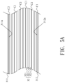
- the configuration of the electricity supply unit 32 mentioned may be the stacking structure of one cathode electrode layer 321, one separator layer 323 and one anode electrode layer 322 or be the stacking structure of several cathode electrode layers 321, several separator layers 323 and several anode electrode layers 322 as shown in FIG 5A .
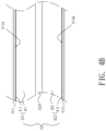
- the configuration of the electricity supply unit 32' can be the winding structure as shown in FIG. 5B .
- the configuration of the electricity supply unit 32 mentioned in this invention may be any kinds of structures without limitation because the major difference between this invention and the prior art is the electrical connection between the electricity supply unit 32 and the package structure 31 while there is no any electrical connection between the current electricity supply system and the current package structure.
- the package structure 31 includes at least two terminals T1 and T2.
- One end of the terminal T1 is electrically connected to the cathode electrode layer 321 of the electricity supply unit 32 while another end of the terminal T1 is located on the first substrate 311 of the package structure 31 and acts as a connection point to connect to the peripherals (not shown).
- One end of the terminal T2 is electrically connected to the anode electrode layer 322 of the electricity supply unit 32 while the other end of the terminal T2 is located on the second substrate 312 of the package structure 31 and acts as a connection point to connect to the peripherals (not shown).
- the terminals T1 and T2 can be located on the same substrate 311 or 312 or located on the different substrate 311 or 312. As illustrated in FIG.
- the terminal T1 is located on the first substrate 311 and the terminal T2 is located on the second substrate 312.
- the electrode layer 321 is electrically connected to the terminal T1 due to the electrical connection between the conductive surface 311a of the substrate 311 and the electrode layer 321 of the electricity supply unit 32.
- the electrode layer 322 is electrically connected to the terminal T2 due to the electrical connection between the conductive surface 312a of the substrate 312 and the electrode layer 322 of the electricity supply unit 32.
- the electrical connections between the terminal T1 and the electrode 321 and between the terminal T2 and the electrode 322 can be implemented by direct circuit layout or any conductive components. In FIG.
- the two terminals T1 and T2 are located on the same substrate 311 or 312 so that the electrode layers 321 and 322 are individually electrical connected to the terminals T1 and T2 due to the electrical connection between the conductive surfaces 311a and 312a of the substrates 311 and 312 and the electrode layers 321 and 322 of the electricity supply unit 32.
- the conductive element 6 such as the conductive glue
- the electrical power generated by the electrode layer 321 of the substrate 311 is able to be transferred from the terminal T1 on the conductive surface 311a of the substrate 311 to the terminal T2 on the conductive surface 312a of the substrate 312.
- the package structure mentioned above mainly has four functions.
- the first function is to seal the electricity supply system completely inside the package structure.
- a great amount of the electrolyte must be impregnated by the electricity supply system to make the chemical-electrical reactions occurring inside the electricity supply system can be workable.
- the polarities of the sealing frame and the electrolyte are different from each other so that after forming the first silicone layers on to the two substrates and forming the second silicone layer on to at least one first silicone layer, the adhesion layers stained with the electrolyte still can be able to adhere to each other because the electrolyte staining on the adhesion layers would be repelled.
- the second function is to reduce the possibility of the lithium metal formation. The main reason of this is because the material of the sealing frame is not metal but polymer. As the electrochemical reactions occurring around 0V, the lithium ions would be easy to form the lithium metal if the lithium ions contact with the metal material such as copper or nickel.
- the third function is to provide excellent flexibility even after thermal curing process.
- the sealing frame is mainly silicone, the material is not the thermal plastic materials and this is why the sealing frame would be able to keep its flexibility even under the thermal treatments.
- the forth function is to increase the moisture resistant ability.
- the sealing frame is a kind of the hydrophobic component. Since the sealing frame is hydrophobic, the moisture inside the sealing frame can only be transferred by diffusing. Until the moisture entirely diffuses into sealing frame, that is, the moisture concentration of the sealing frame has been reached to saturation, and then the moisture would be able to penetrate into the electricity supply system inside the package structure gradually. Hence, the sealing frame is helpful for slowing down the speed of moisture penetration. As illustrated in FIG.
- the package structure of this invention gets higher moisture content at the first 7-day test but indeed gets much lower moisture content at the 14-day test and at the 21-day test as well.
- the first 7-day result can be taken as one-year usage of the package structure under normal condition (the package structure is operated under the room temperature and moisture for one year) while the 14-day result and the 21-day result reveal the two-year usage condition and the three-year usage condition individually.
- the package structure shows better ability of moisture resistance for long-time usage.
- the electricity supply system can be directly integrated with the circuit broad and also can be processed by the normal PCB or SMT processes.
- the electricity supply system can be taken as an element of SMT so that the SMT processes are able to be exerted for manufacturing the electricity supply system and of course, the process cost can be reduced.
- the surfaces of the substrates can be used for laying some peripheral electronic elements or electrical circuits, the dimensions of the electronics can be much smaller and thinner.
Description
- This application is a continuation-in-part (CIP) of
U.S. patent application Ser. No. 15/806,940, filed on November 8, 2017 U.S. patent application Ser. No. 15/141,826, filed on April 29, 2016 - The present invention relates to a package structure and its related electricity supply system and especially is related to a package structure and its related electricity supply system having a brand new electrical conduction module and excellent abilities of moisture resistance and gas resistance.
- In the electronic device industry, portability and wireless design are the major trends. Except the lighter, thinner and smaller designs, the flexibility of the electronics is highly focused as well. Hence, an electricity supply system having smaller volume, lighter weight and higher energy density is imperatively required. However, to prolong the life and to increase the energy density of the electricity supply system, the primary electricity supply system obviously can not satisfy the demands of the current electronics. And this is the reason why the secondary electricity supply systems such as the lithium battery system, fuel cell system, solar cell system become the main stream for their recharge abilities. The lithium battery system is taken as the example for its highly development.
-
FIG. 1 illustrates the current cell of the lithium battery system. The main structure is constructed by a separator layer sandwiched by a cathode electrode and an anode electrode. The external electrodes of the whole lithium battery system, which are electrically connected to the peripherals, are welded individually to the tabs located in the current collectors of both cathode and anode electrodes. As shown inFIG. 1 , thelithium battery 1 includes aseparator layer 11, a firstactive material layer 12, a secondactive material layer 13, a firstcurrent collector layer 14, a secondcurrent collector layer 15 and apackage unit 16. The firstactive material layer 12 is located above theseparator layer 11. The firstcurrent collector layer 14 is located above the firstactive material layer 12. The secondactive material layer 13 is located under theseparator layer 11. The secondcurrent collector layer 15 is located under the secondactive material layer 13. Thepackage unit 16 seals the whole stacking structure mentioned above except the twotabs lithium battery 1 provides the electricity to an electronic device 2 (the circuit broad illustrated inFIG. 1 is only one embodiment and is not a limitation for the electronic device 2), thetabs electricity input terminals electronic device 2 so that the electricity stored in thelithium battery 1 is transferred to theelectronic device 2. After that, the electricity is transferred to theelement area 23 of theelectronic device 2 by the layouts. Theelement area 23 mentioned here may be the circuit layouts or the surface mounted elements, that is, typically includes the logical circuit, active elements, and passive elements and so on. However, the electrical and safety performances of thelithium battery 1 are dramatically influenced by the characteristics of both the interface between theseparator layer 11 and the firstactive material layer 12 and the interface between theseparator layer 11 and the secondactive material layer 13. For the current lithium battery system, the characteristics of these interfaces are controlled either by solid stacking method or by high-tension winding method to ensure the good electrical and safety performances of the lithium battery system. Unfortunately, the lithium battery systems made by solid stacking or high-tension winding method are definitely lack of flexibility and even are impossible to be flexed. If the stacked battery or the winded battery is forced to be flexed would cause the serious damage to the interfaces between theseparator layer 11 and the firstactive material layer 12 and theseparator layer 11 and the secondactive material layer 13. - As for the current package unit of the current electricity supply system, no matter for the primary battery system or for the secondary battery system, most of the packages of the battery system are with the hard metal cases including the cylindrical cases and prismatic cases. For example, most of the battery systems exerted in the current notebooks are the lithium battery in shape of 18650 cylinders with hard metal cases; most of the battery systems exerted in the current portable communication devices are the lithium battery in the shape of 383562 prisms with hard metal cases. The advantages of the hard metal case are to prevent the cell from the external force and also to reduce the influence of the environmental factors such as the moisture and oxygen and so on. Hence, for the terminal electronics, the secondary battery systems are indeed able to provide better electrical performance and better safety performance but the fixed size and the hard case become the serious limitations for matching with most of the electronics. Although a soft-pack lithium battery system had been developed for reducing the difficulties of exerting in the current electronics, the soft-pack lithium battery system, comparing to the lithium battery systems having the hard metal packages, has to be sealed by a hot pressing procedure so that the interface between the metal tab and soft package would be poor because the material of the tab is metal while the material of the soft package is thermal-sealing polymer. Naturally, the abilities of gas resistance, especially for oxygen, and of moisture resistance of the soft package would be worse than the hard metal case with welding sealing. Furthermore, after several times of charging and discharging, the dimensions of the whole battery system have to suffer expansion and shrinkage alternatively. Due to the weaker stress of the material of the soft package, the secondary battery having the soft package is not able to maintain its own dimension and this disadvantage would be the killing problem for circuit design of the electronics.
- As illustrated in
FIG. 1 , theseparator layer 11 between the firstactive material layer 12 and the secondactive material layer 13 is mainly used for preventing the direct connection between the first electrode substrate (including the firstactive material layer 11 and the first current collector layer 14) and the second electrode substrate (including the secondactive material layer 13 and the second current collector layer 15). Once the first electrode substrate connects to the second electrode substrate directly, thelithium battery 1 would have the inner shortage problem. However, since the ion migrations inside thelithium battery 1 are still needed, the material of theseparator layer 11 must be electrically insulated as well as porous so that the most popular materials of theseparator layer 11 are PVC, PC and any other polymers. Besides, according to the glass transition temperature and softening temperature of the different polymers or one polymer with different molecular weights, the partial structure of the polymer may be changed within a certain range of the temperature. Hence, when the inner temperature of the battery system is increased due to the inner shortage or the external shortage or any other reasons, the structure of theseparator layer 11 would be changed to block the paths of ion migrations inside thelithium battery 1 for avoiding the reactions under the high temperature and further reducing the possibility of explosion of thelithium battery 1. If the inner temperature of thelithium battery 1 still increases under certain reasons, the structure of theseparator layer 11 would be totally melted till the inner temperature reaches to 150°C to 180°C. In this case, the meltedseparator layer 11 would not be able to provide any protections between the first electrode substrate and the second electrode substrate so that thelithium battery 1 would be entirely short and even gets on fire or explodes. Apparently, thecurrent separator layer 11 is a great threat to the safety of thelithium battery 1. - Besides the disadvantages mentioned above, the most important is almost all the circuits and elements are designed as flexible for matching with the flexible devices except for the battery system. Till now, the flexibility of the battery system can not coexist with the good electrical and safety performances. Meanwhile, the dimensions of the battery system are not easy to meet the requirements of smaller and thinner so that most of the electronics have to reserve a space for the battery system and this would make the dimensions of the electronics become much more difficult to be reduced.
-
US 2011/217570 ,CN 201673947 andUS 2018/069271 disclose a package structure and its related electricity supply system are disclosed. Two substrates of the package structure are directly or indirectly served as current collectors of the electricity supply system. The sealing frame of the package structure is made of several adhesive layers having high moisture-resistance and/or high gas-resistance. Hence, the package structure mentioned may not only provide a novel electrical conduction module to lower the intrinsic impedance of the electricity supply system itself but prevent the moisture and the gas outward from the electricity supply unit inside the package structure as well. Consequently, the electrical performance and safety of the electricity supply system are both improved. However, in this application, the details of the sealing frame is not disclosed. -
EP 2604667 discloses a side package structure of electronic modules including a upper substrate, a lower substrate and a sealing frame. The sealing frame is disposed between the upper substrate and the lower substrate to form a space thereof. The sealing frame is made of silicone to improve moisture barrier and to retard the permeation of water vapor. Also, the erosion of polar solvent and plasticizer is avoided due to the characteristic of the silicone. In this application, the chemical formulas are taught, however, the thickness of the sealing frame is not disclosed. - It is an objective of this invention to provide a package structure and its related electricity supply system. The package mentioned in this invention acts as a sealing frame to block the moisture and gas from outsides so that the chemical and the electrical reactions of the electricity supply unit would not be affected.
- Another objective of this invention is to provide a package structure and its related electricity supply system. The sealing frame may be rapidly and precisely formed on the first substrate and the second substrate by screen printing or coating. The package structure mentioned in this invention may be produced under higher yield rate and faster production rate.
- It is an objective of this invention to provide a package structure and its related electricity supply system. The electricity supply system is able to directly electrically connected to the external electrical elements so that the amounts of the elements exerted in the electronic may be reduced and the dimensions of the electronics are able to become smaller and thinner as well.
- It is an objective of this invention to provide a package structure and its related electricity supply system. The package structure can be integrated with the electricity supply unit so that the materials used are reduced and the production cost of the electronics can be reduced as well.
- It is an objective of this invention to provide a package structure and its related electricity supply system. Once the electricity supply system is impacted by the external forces, the electricity supply unit would be immediately separated from the package structure to form a protective open circuit so that the safety performance of the electricity supply system is increased.
- Another objective of this invention is to provide a package structure and its related electricity supply system. The package structure may be integrated with the electricity supply unit so that the amounts of the total interfaces inside the electricity supply system are reduced to reduce the inner resistance of the electricity supply system and to increase the electrical performance of the electricity supply system as well.
- In order to implement the abovementioned, this invention discloses a package structure and its related electricity supply system. A flexible sealing frame is exerted to seal a space between the first substrate and the second substrate so that the electricity supply unit placed inside the space can be totally isolated from the external moisture and gas to ensure the electrical and safety performances of the electricity supply system. At least one of the first substrate and the second substrate can be a circuit broad and electrically connects to the peripheral electronics so that the amounts of the elements exerted inside the electronics may be reduced to implement the designs of smaller and thinner.
- The first electrode includes a first active material layer and a first current collector. The first current collector is directly contacted to the first active material layer and has a first sealing region. The second electrode includes a second active material layer and a second current collector. The second current collector is directly contacted to the second active material layer and has a second sealing region. The flexible sealing frame is disposed between the first sealing region of the first current collector and the second sealing region of the second current collector. The flexible sealing frame is used for adhering the first current collector to the second current collector to provide an enclosed space to accumulate the first active material, the second active material and the separator layer.
- The flexible sealing frame includes two first silicone layers and a second silicone layer. The first silicone layers mainly contain a chemical formula I of:

- The second silicone layer mainly contains a chemical formula II of:

- Both the first silicone layers and the second silicone layer contain the chemical formula I and the chemical formula II. This solves the problems of bubbles or the substrate easily peeling off. The interfacial tension and the polarity of silicone are modified of the modified silicone cured layer to enhance the adhesion for different materials. Moreover, the sealing frame is flexible after sealing and can totally match with the flexible electricity supply unit placed inside. And of course, the package structure can meet the requirement of the flexible electronics.
- Further scope of applicability of the present invention will become apparent from the detailed description given hereinafter. However, it should be understood that the detailed description and specific examples, while indicating preferred embodiments of the invention, are given by way of illustration only, since various changes and modifications within the scope of the invention will become apparent to those skilled in the art from this detailed description.
- The present invention will become more fully understood from the detailed description given hereinbelow illustration only, and thus are not limitative of the present invention, and wherein:
-
FIG. 1 illustrates the example of the cell of the prior-art lithium battery system. -
FIG. 2A illustrates the package structure of the electricity supply system of the present invention. -
FIG. 2B illustrates the cross-section view configuration along the A-A' line inFIG. 2A . -
FIG. 3 illustrates an embodiment that the first substrate of the package structure serves as a circuit broad of the present invention. -
FIG. 4A illustrates an embodiment that the conductive surface of the substrate serves as a current collector layer of the present invention. -
FIG. 4B illustrates an embodiment that the conductive surface of the substrate dose not serve as a current collector layer of the present invention. -
FIG. 5A illustrates the cross-section configuration of the electricity supply system having the multi-layer electrode placed inside the package structure of the present invention. -
FIG. 5B illustrates the cross-section configuration of the electricity supply system having the winding type electrode placed inside the package structure of the present invention. -
FIG. 6A illustrates an embodiment that two terminals of the electricity supply system are located on two different substrates of the present invention. -
FIG. 6B illustrates an embodiment that two terminals of the electricity supply system are located on one substrate of the present invention. -
FIG. 7 illustrates the aging test result of both the prior-art and the present package structures under the aging test condition of the temperature at 60°C and the moisture at 95%RH. -
FIG. 8 illustrates the cross-section view configuration along the A-A' line inFIG. 2A . -
FIG. 9A illustrates the first conductive surface of the first substrate of the present invention, showing an embodiment of the first sealing region. -
FIG. 9B illustrates the second conductive surface of the second substrate of the present invention, showing an embodiment of the second sealing region. -
FIG. 2A illustrates the appearance of the package structure of the electricity supply system of this invention andFIG. 2B illustrates the cross-section view along the A-A' line of theFIG. 2A . Thepackage structure 31 of this invention is used for placing anelectricity supply unit 32. Thepackage structure 31 includes afirst substrate 311, asecond substrate 312 and asealing frame 313. Thepackage structure 31 can be directly exposed in the general environment and has the ability to resist external forces and moisture penetration. Thefirst substrate 311 has at least one firstconductive surface 311a and thesecond substrate 312 has at least one secondconductive surface 312a. The sealingframe 313 surrounds the edges between thefirst substrate 311 and thesecond substrate 312 so that there is a space S formed among the sealingframe 313, thefirst substrate 311 and thesecond substrate 312. The space S is used for placing theelectricity supply unit 32. - The
electricity supply unit 32 is electrically connected to the firstconductive surface 311a of thefirst substrate 311 as well as connected to the secondconductive surface 312a of thesecond substrate 312. The sealingframe 313 includes twofirst silicone layers 313a and asecond silicone layer 313b. Twofirst silicone layers 313a adhere to thefirst substrate 311 and thesecond substrate 312 respectively. That is, thefirst substrate 311 and thesecond substrate 312 adhere to one offirst silicone layers 313a respectively. Thesecond silicone layer 313b is located between the twofirst silicone layers 313a to stick the twofirst silicone layers 313a, that is, thefirst silicone layer 313a attached to thefirst substrate 311 and thefirst silicone layer 313a attached to thesecond substrate 312 are adhered to each other by thesecond silicone layer 313b. - Furthermore, please refer to
FIG. 9A , the firstconductive surface 311a of thefirst substrate 311 has afirst sealing region 311b, which is defined along the circumference of the firstconductive surface 311a. The remaining area of the firstconductive surface 311a of thefirst substrate 311, surrounded by thefirst sealing region 311b, is primarily to provide as the contact area for the first active material layer. One of thefirst silicone layer 313a is adhered to thefirst sealing region 311b. please refer toFIG. 9B , the secondconductive surface 312a of thesecond substrate 312 has asecond sealing region 312b, which is defined along the circumference of the secondconductive surface 312a. The otherfirst silicone layer 313a is adhered to thesecond sealing region 312b. The remaining area of the secondconductive surface 312a of thesecond substrate 312, surrounded by thesecond sealing region 312b, is primarily to provide as the contact area for the second active material layer. - To make the
first silicone layers 313a and thesecond silicone layer 313b with different adhesion property, different additives or formulas are used to modify the adhesion property of thefirst silicone layers 313a and thesecond silicone layer 313b. The interfacial tension and the polarity of silicone of thefirst silicone layer 313a are modified, depending on the materials of the firstconductive surface 311a and the secondconductive surface 312a, to enhance the adhesion for different materials. The adhesion force of thefirst adhesion 313a between surfaces with different materials, such as metal substrates and silicone, i.e. thesecond silicone layer 313b, is improved. Therefore, thefirst silicone layer 313a are adhered firmly between thefirst substrate 311 and thesecond substrate 312. On the other hand, the second silicone layer 131b is used to adhere twofirst silicone layers 313a. Therefore, the adhesion force of thesecond adhesion 313b between surfaces with the same materials or property, is improved. Thus, thefirst substrate 311 and thesecond substrate 312 are adhered firmly by thefirst silicone layers 313a and thesecond silicone layer 313b. And the space S, formed among the sealingframe 313, thefirst substrate 311 and thesecond substrate 312, would be totally isolated from the external moisture and gas to ensure the electrical and safety performances of the electricity supply system. - The
first silicone layers 313a mainly contain a chemical formula I of:
- The
second silicone layer 313b mainly contains a chemical formula II of:
- Both the
first silicone layers 313a and thesecond silicone layer 313b contain both the chemical formula I and the chemical formula II. - Amounts of the chemical formula I within each of the
first silicone layers 313a is greater than amounts of the chemical formula II within each of thefirst silicone layers 313a. Amounts of the chemical formula II within thesecond silicone layer 313b is greater than amounts of the chemical formula I within thesecond silicone layer 313b. - Also, amounts of the chemical formula II within the
second silicone layer 313b is greater than amounts of the chemical formula II within thefirst silicone layers 313a by 0.1% to 60%, on a weight/volume basis. Thefirst silicone layers 313a are modified by increasing a proportion of addition-type silicone and/or by adding epoxy, acrylic acid or a combination thereof into silicone. - As an example of the forming method, the
first silicone layers 313a are formed on the firstconductive surface 311a of thefirst substrate 311, and the secondconductive surface 312a of thesecond substrate 312 respectively, by the screen printing method or the coating method, for example. Then, surface characteristics of the firstconductive surface 311a and the secondconductive surface 312a are modified to enhance bonding ability with the second silicone layers 313b in the subsequent process. In the other words, thefirst silicone layers 313a can be considered as the surface-modified layer of thefirst substrate 311 and thesecond substrate 312 respectively. Furthermore, thefirst silicone layers 313a are adhered along their inner circumferences of the firstconductive surface 311a and the secondconductive surface 312a. - Then the polymerization is performed slowly for curing. Since one side of the
first silicone layers 313a is free and the slowly curing process is performed, the produced gas can be exhausted. Also, thefirst silicone layers 313a are modified depending on the materials of the firstconductive surface 311a of thefirst substrate 311, and the secondconductive surface 312a of thesecond substrate 312 respectively. The good adhesion situations are presented on the interfaces between thefirst silicone layers 313a and thefirst substrate 311, and thefirst silicone layers 313a and thesecond substrate 312. - The second silicone layers 313b is disposed on one of the
first silicone layers 313a. Then, thefirst substrate 311 and thesecond substrate 312, together with the second silicone layers 313b and thefirst silicone layer 313a, are combined. This polymerization is performed in two stages to bond together firmly. In addition, a pressing step can be combined with the polymerization process. The heat treatment temperature of first stage is lower than the heat treatment temperature of second stage. The heat treatment duration of first stage is longer than the heat treatment duration of second stage. During the lower temperature of the first stage, the chemical formula II of thesecond silicone layers 313b is the dominant component to form a crystalline structure in the second silicone layers 313b. Due to the thickness of thesecond silicone layers 313b is thin, the crystalline structure is essentially regarded as the main moisture-blocking structure of the second silicone layers 313b. The crystalline structure can enhance the moisture-blocking ability of the interfaces between the second silicone layers 313b and any one of thefirst silicone layer 313a. It is very important capability for package structure of the electricity supply system, such as the lithium battery. - During the higher temperature of the second stage, the chemical formula I of the
second silicone layers 313b is the dominant component and has better bonding ability than the chemical formula II. Therefore, the second silicone layers 313b and thefirst silicone layers 313a are bonded together firmly. Preferably, the heat treatment temperature of first stage is lower than the heat treatment temperature of second stage by 30 to 70 degrees C°. The heat treatment duration of first stage is longer than the heat treatment duration of second stage by 80 to 300 seconds. To prevent the second silicone layers 313b to be deformed during above-mentioned process, the second silicone layers 313b further includes a spacer. The spacer includes silicon dioxide particles, titanium oxide particles or a combination thereof. - Since the second silicone layers 313b is disposed between the
first silicone layers 313a, which are made of the same or substantially the same material, i.e. silicone, the adhesion force therebetween is high. Even though gas is produced, the adhesion structure is not easily weakened. Also, silicone is not as dense as thefirst substrate 311 and thesecond substrate 312. In micro-view, the silicone has larger hole inside than the materials of thefirst substrate 311 and thesecond substrate 312. Even though the second silicone layers 313b is disposed between thefirst silicone layers 313a for curing, the produced gas is easily exhausted from thefirst silicone layers 313a, and does not readily collect to form bubbles. The intermolecular forces between the second silicone layers 313b and thefirst silicone layers 313a are equal. The gas flows inside are uniform. The gas bubbles will not easily merge to form larger ones. Therefore, the good adhesion situations are presented on the interfaces between thefirst silicone layers 313a and the second silicone layers 313b. The interfaces between thefirst silicone layers 313a and thefirst substrate 311, and thefirst silicone layers 313a and thesecond substrate 312 are secured better interface adhesion than the conventional interfaces. - At least one of the
first substrate 311 and thesecond substrate 312 is a circuit broad, such as the printed circuit broad, multi-layer circuit broad and flexible printed circuit broad and so on, or a metal layer. No matter for thefirst substrate 311 or thesecond substrate 312, at least one of thefirst substrate 311 and thesecond substrate 312 must have a conductive surface (the firstconductive surface 311a and/or the secondconductive surface 312a) to electrically connects to theelectricity supply unit 32 placed inside thepackage structure 31 so that the electrical power generated by theelectricity supply unit 32 is collected by the conductive surface (the firstconductive surface 311a and/or the secondconductive surface 312a) and furthermore, the electrical power collected may be transferred to the circuit broad according to the different mechanical designs. For example,FIG. 3 illustrates one of the possible embodiments, as for the substrate (thefirst substrate 311 as the example here) acting as the circuit broad and having one conductive surface (the firstconductive surface 311a as the example here), the electrical power collected can be directly transferred to the circuit broad (the first substrate 311) by the conductive surface (the firstconductive surface 311a). As for the substrate (thesecond substrate 312 as the example here) only having one conductive surface (the secondconductive surface 312a as the example here), the electrical power collected is transferred by the electrical connection between the two substrates (thefirst substrate 311 and the second substrate 312). At last, a complete loop is formed within theelectricity supply unit 32 and the electrical power may be transferred to theelement 5 laid on the circuit broad (the first substrate 311). If both thefirst substrate 311 and thesecond substrate 312 are circuit broads, the electrical connection between thefirst substrate 311 and thesecond substrate 312 not only being used for providing electrical power but acting as the electrical path for elements laid on thefirst substrate 311 and thesecond substrate 312 as well. However, besides acting as the circuit broads, thefirst substrate 311 and thesecond substrate 312 can also act as the metal substrates, the glass substrates, the composite substrates such as the metal-polymer composite substrates and so on. - The
electricity supply unit 32 mentioned above includes at least twoelectrode layers separator layer 323. The twoelectrode layers FIG. 2B ). In other embodiment, one of the two electrode layers 321,322 is disposed to directly contact to the sealing frame 313(as shown inFIG. 8 ), usually an anode electrode layer. InFIG.8 , theelectrode layer 321 which does not directly contact to thesealing frame 313 is usually a cathode electrode layer. Also, a part of the firstconductive surface 311a is exposed between the sealingframe 313 and theelectrode layer 321 because theelectrode layer 321 does not directly contact to thesealing frame 313. Theelectricity supply unit 32 is a lithium-ion conductive function layer for a lithium cell. - The
first silicone layers 313a are utilized to support theelectricity supply unit 32 to get a balance stress relationship between the electrode layers 321, 322. Therefore, the thickness of thefirst silicone layers 313a is close to the thickness of the electrode layers 321, 322. Each of thefirst silicone layers 313a has a thickness ranging from 70 percent to 90 percent with respect to the sum of the thickness of theseparator layer 323 and the first active material layer (the electrode layer 321) or with respect to the sum of the thickness of theseparator layer 323 and the second active material layer (the electrode layer 322). Preferably, each of thefirst silicone layers 313a has a thickness ranging from 80 percent to 85 percent with respect to the sum of the thickness of theseparator layer 323 and the first active material layer (the electrode layer 321) or with respect to the sum of the thickness of theseparator layer 323 and the second active material layer (the electrode layer 322). - The
second silicone layer 313b is served as a bonding layer in the invention and its thickness is a setting value, not varied depending on thefirst silicone layers 313a. The thickness of thesecond silicone layers 313b is 0.5 µm to 2.5 µm. When the thickness of thesecond silicone layers 313b is too thin, i.e. thinner than 0.5 µm, the adhesion will be too weak. When the thickness of thesecond silicone layers 313b is too thick, i.e. thicker than 2.5 µm, the water barrier effect would be too worse. Preferably, the thickness of thesecond silicone layers 313b is 1 µm to 2 µm. - Each
separator layer 323 is located between the adjacent twoelectrode layers separator layer 323 is to prevent theelectrode layer 321 directly connected to theelectrode layer 322. The electrode layers 321 and 322 and theseparator layer 323 are all moistened by the electrolyte including the liquid-phase electrolyte, gel type electrolyte and solid-phase electrolyte. The materials of theseparator layer 323 include the polymers, the ceramics or the glass fibers. - The
electrode layer 321 includes an active material layer A1 and theelectrode layer 322 includes an active material layer A2. As illustrated inFIG. 4A , thefirst substrate 311 has the firstconductive surface 311a, served as a first current collector, and thesecond substrate 312 has the secondconductive surface 312a, served as a second current collector. The active material layer A1 is directly contacted to or formed on the firstconductive surface 311a of thefirst substrate 311 and the active material layer A2 is directly contacted to or formed on the secondconductive surface 312a of thesecond substrate 312. That is, there is no any other structure exists between the active material layer A1 and the firstconductive surface 311a of thefirst substrate 311; there is no any other structure exists between the active material layer A2 and the secondconductive surface 312a of thesecond substrate 312 either. The formation method for the active material layers A1 and A2 may include that the active material layers A1 and A2 are directly formed on theconductive surface conductive surface conductive surface first substrate 311 and 312 (both of thesubstrate FIG. 4B , the current collector layers illustrated are independent components comparing to the current collector layers illustrated inFIG. 4A are one part of the substrates. The current collector layers C1 and C2 illustrated inFIG. 4B are independent components while theconductive surfaces substrates FIG. 4B . In the embodiment shown inFIG. 4B , the definition of theelectrode layer 321 includes the active material layer A1 and the current collector layer C1 and the active material layer A1 is formed on the current collector layer C1. The definition of theelectrode layer 322 includes the active material layer A2 and the current collector layer C2 and the active material layer A2 is formed on the current collector layer C2. The electrical connection between theelectricity supply unit 32 and thepackage structure 31 is implemented by the direct connection between the current collector layers C1 and C2 and theconductive surfaces substrates conductive surfaces substrates conductive surfaces substrates - Accordingly, the
package structure 31 of this invention is electrically connected to theelectricity supply unit 32 and the electrical connection between theelectricity supply unit 32 and thepackage structure 31 may be the direct electrical connection or the indirect electrical connection. Such design for thepackage structure 31 and theelectricity supply unit 32 may not only greatly increase the contact area of the electrical connection but dramatically decrease the resistance of theelectricity supply unit 32 as well. At the same time, as theelectricity supply system 3 is damaged due to impacting, falling down or nail penetrating and so on, the active material layers A1 and A2 of the electrode layers 321 and 322 and/or the current collector layers C1 and C2 of the electrode layers 321 and 322 would be immediately separated from the electrode layers 321 and 322 for the occurrences of the partial high temperature or the broken structure. So, the electrical connection between theelectricity supply unit 32 and thepackage structure 31 would be entirely destroyed, that is, the wholeelectricity supply system 3 would be under the open circuit state so that the chemical reactions inside theelectricity supply unit 32 can be terminated to avoid the explosion or firing of theelectricity supply system 3 due to the serious of the chain reactions occurring inside theelectricity supply unit 32. - The configuration of the
electricity supply unit 32 mentioned may be the stacking structure of onecathode electrode layer 321, oneseparator layer 323 and oneanode electrode layer 322 or be the stacking structure of several cathode electrode layers 321,several separator layers 323 and several anode electrode layers 322 as shown inFIG 5A . Also, the configuration of the electricity supply unit 32' can be the winding structure as shown inFIG. 5B . Of course, the configuration of theelectricity supply unit 32 mentioned in this invention may be any kinds of structures without limitation because the major difference between this invention and the prior art is the electrical connection between theelectricity supply unit 32 and thepackage structure 31 while there is no any electrical connection between the current electricity supply system and the current package structure. - The
package structure 31 includes at least two terminals T1 and T2. One end of the terminal T1 is electrically connected to thecathode electrode layer 321 of theelectricity supply unit 32 while another end of the terminal T1 is located on thefirst substrate 311 of thepackage structure 31 and acts as a connection point to connect to the peripherals (not shown). One end of the terminal T2 is electrically connected to theanode electrode layer 322 of theelectricity supply unit 32 while the other end of the terminal T2 is located on thesecond substrate 312 of thepackage structure 31 and acts as a connection point to connect to the peripherals (not shown). The terminals T1 and T2 can be located on thesame substrate different substrate FIG. 6A , the terminal T1 is located on thefirst substrate 311 and the terminal T2 is located on thesecond substrate 312. Theelectrode layer 321 is electrically connected to the terminal T1 due to the electrical connection between theconductive surface 311a of thesubstrate 311 and theelectrode layer 321 of theelectricity supply unit 32. Theelectrode layer 322 is electrically connected to the terminal T2 due to the electrical connection between theconductive surface 312a of thesubstrate 312 and theelectrode layer 322 of theelectricity supply unit 32. And the electrical connections between the terminal T1 and theelectrode 321 and between the terminal T2 and theelectrode 322 can be implemented by direct circuit layout or any conductive components. InFIG. 6B , the two terminals T1 and T2 are located on thesame substrate conductive surfaces substrates electricity supply unit 32. In this way, by theconductive element 6 such as the conductive glue, the electrical power generated by theelectrode layer 321 of thesubstrate 311 is able to be transferred from the terminal T1 on theconductive surface 311a of thesubstrate 311 to the terminal T2 on theconductive surface 312a of thesubstrate 312. - The package structure mentioned above mainly has four functions. The first function is to seal the electricity supply system completely inside the package structure. As is known to all, a great amount of the electrolyte must be impregnated by the electricity supply system to make the chemical-electrical reactions occurring inside the electricity supply system can be workable. Fortunately, the polarities of the sealing frame and the electrolyte are different from each other so that after forming the first silicone layers on to the two substrates and forming the second silicone layer on to at least one first silicone layer, the adhesion layers stained with the electrolyte still can be able to adhere to each other because the electrolyte staining on the adhesion layers would be repelled. In this way, the adhesion ability of the first silicone layer to the substrate and the adhesion ability of the first silicone layer to the second silicone layer would not be affected even the electricity supply system is soaked in a great amount of electrolyte. Besides, by the repellence of the electrolyte and the adhesion layers, most of the electrolyte would be kept inside the electricity supply system during pressing process. The second function is to reduce the possibility of the lithium metal formation. The main reason of this is because the material of the sealing frame is not metal but polymer. As the electrochemical reactions occurring around 0V, the lithium ions would be easy to form the lithium metal if the lithium ions contact with the metal material such as copper or nickel. The third function is to provide excellent flexibility even after thermal curing process. Because the material of the sealing frame is mainly silicone, the material is not the thermal plastic materials and this is why the sealing frame would be able to keep its flexibility even under the thermal treatments. The forth function is to increase the moisture resistant ability. Also, the sealing frame is a kind of the hydrophobic component. Since the sealing frame is hydrophobic, the moisture inside the sealing frame can only be transferred by diffusing. Until the moisture entirely diffuses into sealing frame, that is, the moisture concentration of the sealing frame has been reached to saturation, and then the moisture would be able to penetrate into the electricity supply system inside the package structure gradually. Hence, the sealing frame is helpful for slowing down the speed of moisture penetration. As illustrated in
FIG. 7 , comparing to the prior art, under the aging test conditions of the temperature at 60°C and the moisture at 95%RH, the package structure of this invention gets higher moisture content at the first 7-day test but indeed gets much lower moisture content at the 14-day test and at the 21-day test as well. According to this aging test, the first 7-day result can be taken as one-year usage of the package structure under normal condition (the package structure is operated under the room temperature and moisture for one year) while the 14-day result and the 21-day result reveal the two-year usage condition and the three-year usage condition individually. Obviously, the package structure shows better ability of moisture resistance for long-time usage. - Since the two substrates of the package structure are directly or indirectly served as current collectors of the electricity supply system, the electricity supply system can be directly integrated with the circuit broad and also can be processed by the normal PCB or SMT processes. For example, the electricity supply system can be taken as an element of SMT so that the SMT processes are able to be exerted for manufacturing the electricity supply system and of course, the process cost can be reduced. Besides, because the surfaces of the substrates can be used for laying some peripheral electronic elements or electrical circuits, the dimensions of the electronics can be much smaller and thinner.
- The invention being thus described, it will be obvious that the same may be varied in many ways. Such variations are not to be regarded as a departure from the scope of the invention, and all such modifications as would be obvious to one skilled in the art are intended to be included within the scope of the following claims.
Claims (13)
- An electricity supply system, comprising:a first electrode, having a first active material layer and a first current collector directly contacted to the first active material layer and having a first sealing region;a second electrode, having a second active material layer and a second current collector directly contacted to the second active material layer and having a second sealing region;a separator layer, located between the first electrode and the second electrode layer; anda flexible sealing frame, disposed between the first sealing region of the first current collector and the second sealing region of the second current collector, wherein the flexible sealing frame adheres the first current collector to the second current collector for providing an enclosed space to accumulate the first active material, the second active material and the separator layer, the flexible sealing frame comprising:two first silicone layers, one of the first silicone layers adhering to the first sealing region of the first current collector, and the other one of the first silicone layers adhering to the second sealing region of the second current collector, wherein each of the first silicone layers mainly contains a chemical formula I of:
 a second silicone layer, located between the two first silicone layers to adhere therebetween, wherein the second silicone frame mainly contains a chemical formula II of:
 wherein both the first silicone layers and the second silicone layer contain the chemical formula I and the chemical formula II;wherein each of the first silicone layers has a thickness ranging from 70 percent to 90 percent with respect to the sum of the thickness of the separator layer and the first active material layer or with respect to the sum of the thickness of the separator layer and the second active material layer;wherein a thickness of the second silicone layer is 0.5 µm to 2.5 µm and wherein a thickness of the second silicone layer is a setting value and the setting value is not varied depending on a thickness if the first silicone layer.
 - The electricity supply system of claim 1, wherein the first sealing region of the first current collector is defined along the circumference of the first current collector and the second sealing region of the second current collector is defined along the circumference of the second current collector.
- The electricity supply system of claim 1, wherein at least one of the first current collector and the second current collector is a metal layer of a printed circuit board.
- The electricity supply system of claim 1, wherein the first active material layer is directly contacted to the flexible sealing frame and the second active material layer does not contact to the flexible sealing frame.
- The electricity supply system of claim 4, wherein the first active material layer is an anode active material layer and the second active material layer is a cathode active material layer.
- The electricity supply system of claim 4, wherein the second current collector is exposed between the flexible sealing frame and the second active material layer.
- The electricity supply system of claim 1, wherein the first silicone layers are modified by increasing a proportion of addition-type silicone.
- The electricity supply system of claim 1, wherein the first silicone layers are modified by adding epoxy, acrylic acid or a combination thereof into silicone.
- The electricity supply system of claim 1, wherein the second silicone layer further comprises a spacer, wherein the spacer includes silicon dioxide particles, titanium oxide particles or a combination thereof.
- The electricity supply system of claim 1, wherein amounts of the chemical formula II within the second silicone layer is greater than amounts of the chemical formula II within each of the first silicone layers by 0.1% to 60%, on a weight/volume basis.
- The electricity supply system of claim 1, wherein a thickness of the second silicone layer is 1 µm to 2 µm.
- The electricity supply system of claim 1, wherein each of the first silicone layers has a thickness ranging from 75 percent to 80 percent with respect to the sum of the thickness of the separator layer and the first active material layer or with respect to the sum of the thickness of the separator layer and the second active material layer.
- The electricity supply system of claim 1, wherein the second silicone layer has a moisture-blocking crystalline structure.
Applications Claiming Priority (1)
| Application Number | Priority Date | Filing Date | Title |
|---|---|---|---|
| US16/530,513 US11056743B2 (en) | 2010-10-29 | 2019-08-02 | Electricity supply system and package structure thereof |
Publications (3)
| Publication Number | Publication Date |
|---|---|
| EP3772121A1 EP3772121A1 (en) | 2021-02-03 |
| EP3772121B1 true EP3772121B1 (en) | 2023-08-30 |
| EP3772121C0 EP3772121C0 (en) | 2023-08-30 |
Family
ID=68289846
Family Applications (1)
| Application Number | Title | Priority Date | Filing Date |
|---|---|---|---|
| EP19203124.3A Active EP3772121B1 (en) | 2019-08-02 | 2019-10-14 | Electricity supply system and package structure thereof |
Country Status (7)
| Country | Link |
|---|---|
| EP (1) | EP3772121B1 (en) |
| JP (1) | JP6896043B2 (en) |
| KR (1) | KR102324650B1 (en) |
| CN (1) | CN112331977B (en) |
| ES (1) | ES2961817T3 (en) |
| MX (1) | MX2019013545A (en) |
| RU (1) | RU2730593C1 (en) |
Family Cites Families (21)
| Publication number | Priority date | Publication date | Assignee | Title |
|---|---|---|---|---|
| JPH0547360A (en) * | 1991-08-09 | 1993-02-26 | Yuasa Corp | Thin battery |
| JPH07326228A (en) * | 1994-05-30 | 1995-12-12 | Hitachi Cable Ltd | Heat resistant insulated electric wire |
| JP3717085B2 (en) * | 1994-10-21 | 2005-11-16 | キヤノン株式会社 | Negative electrode for secondary battery, secondary battery having the negative electrode, and method for producing electrode |
| US8029927B2 (en) * | 2005-03-22 | 2011-10-04 | Blue Spark Technologies, Inc. | Thin printable electrochemical cell utilizing a “picture frame” and methods of making the same |
| JP2009245782A (en) * | 2008-03-31 | 2009-10-22 | Tdk Corp | Dye-sensitized solar cell |
| JP5658450B2 (en) * | 2009-11-12 | 2015-01-28 | 川崎重工業株式会社 | Battery system |
| TWI406444B (en) * | 2010-03-05 | 2013-08-21 | Prologium Technology Co | Package structure and its related electricity supply system |
| CN201673947U (en) * | 2010-04-30 | 2010-12-15 | 辉能科技股份有限公司 | Packaging structure of power supply system |
| US20180069271A1 (en) * | 2010-10-29 | 2018-03-08 | Prologium Technology Co., Ltd. | Electricity supply system and package structure thereof |
| TWI472831B (en) * | 2011-12-16 | 2015-02-11 | Prologium Technology Co Ltd | Side package structure of electric modules |
| TWI437931B (en) * | 2011-12-16 | 2014-05-11 | Prologium Technology Co Ltd | Pcb structure |
| CN103188868B (en) * | 2011-12-28 | 2016-07-13 | 辉能科技股份有限公司 | Board structure of circuit |
| CN103187370B (en) * | 2011-12-28 | 2016-06-29 | 辉能科技股份有限公司 | The side packing structure of electronics module |
| KR102039390B1 (en) * | 2012-02-21 | 2019-11-04 | 린텍 가부시키가이샤 | Organic electronic element and method for manufacturing organic electronic element |
| WO2014178590A1 (en) * | 2013-04-29 | 2014-11-06 | 주식회사 엘지화학 | Packaging for cable-type secondary battery and cable-type secondary battery comprising same |
| US10673044B2 (en) * | 2016-10-13 | 2020-06-02 | Prologium Technology Co., Ltd. | Electrical insulator and its related battery |
| CN109585704A (en) * | 2017-09-29 | 2019-04-05 | 辉能科技股份有限公司 | Flexible battery |
| TWI676315B (en) * | 2017-10-20 | 2019-11-01 | 輝能科技股份有限公司 | Composite battery cell |
| CN109980984A (en) * | 2017-12-28 | 2019-07-05 | 九号能源科技有限公司 | A kind of two-dimension flexible micro generation power supply system and preparation method thereof |
| CN108976965A (en) * | 2018-07-18 | 2018-12-11 | 江苏卓岸电源科技有限公司 | A kind of corrosion cell case |
| CN208538852U (en) * | 2018-08-16 | 2019-02-22 | 南昌大学 | A kind of encapsulating products of LED chip |
-
2019
- 2019-10-14 ES ES19203124T patent/ES2961817T3/en active Active
- 2019-10-14 EP EP19203124.3A patent/EP3772121B1/en active Active
- 2019-10-29 JP JP2019196191A patent/JP6896043B2/en active Active
- 2019-11-07 KR KR1020190142066A patent/KR102324650B1/en active IP Right Grant
- 2019-11-13 MX MX2019013545A patent/MX2019013545A/en unknown
- 2019-11-25 RU RU2019137913A patent/RU2730593C1/en active
- 2019-11-29 CN CN201911201143.8A patent/CN112331977B/en active Active
Also Published As
| Publication number | Publication date |
|---|---|
| JP6896043B2 (en) | 2021-06-30 |
| KR20210016256A (en) | 2021-02-15 |
| RU2730593C1 (en) | 2020-08-24 |
| CN112331977B (en) | 2023-03-28 |
| MX2019013545A (en) | 2021-09-21 |
| KR102324650B1 (en) | 2021-11-10 |
| EP3772121C0 (en) | 2023-08-30 |
| BR102019022505A2 (en) | 2021-02-09 |
| ES2961817T3 (en) | 2024-03-14 |
| EP3772121A1 (en) | 2021-02-03 |
| CN112331977A (en) | 2021-02-05 |
| JP2021027024A (en) | 2021-02-22 |
Similar Documents
| Publication | Publication Date | Title |
|---|---|---|
| US8679674B2 (en) | Battery with protective packaging | |
| KR100782162B1 (en) | Reserve battery having all solid state thin film battery | |
| KR101037042B1 (en) | Pouch type secondary battery with enhanced stability | |
| US7235112B2 (en) | Micro-battery fabrication process including formation of an electrode on a metal strip, cold compression and removal of the metal strip | |
| KR20130076882A (en) | Thin film battery with protective packaging | |
| KR20030095266A (en) | Electrochemical element | |
| EP1939962B1 (en) | Electricity supply system | |
| CN101443937A (en) | Thin film battery on an integrated circuit or circuit board and method thereof | |
| KR100858790B1 (en) | Secondary Battery of High Capacity and Excellent Stability | |
| JPH07107840B2 (en) | Organic electrolyte battery | |
| KR101493569B1 (en) | Electricity supply system and electricity supply element thereof | |
| EP1221734B1 (en) | Flexible battery structure | |
| US9105930B2 (en) | Electricity supply system and electricity supply element thereof | |
| US20110217570A1 (en) | Electricity supply system and package structure thereof | |
| JP5227009B2 (en) | Electrical energy supply system | |
| EP3772121B1 (en) | Electricity supply system and package structure thereof | |
| CN1663062A (en) | Battery with vibration-resistant joint between positive electrode and current carrying strap | |
| US11056743B2 (en) | Electricity supply system and package structure thereof | |
| US20180069271A1 (en) | Electricity supply system and package structure thereof | |
| KR20160107060A (en) | Rechargeable battery having connecting member | |
| TWI705598B (en) | Electricity supply system and the package structure thereof | |
| KR101136215B1 (en) | Secondary Battery | |
| KR20070104689A (en) | Secondary battery of improved safety employing electrode assembly covered with separator film | |
| KR20220033944A (en) | The Electrode Assembly And The Secondary Battery | |
| KR101136162B1 (en) | Secondary Battery |
Legal Events
| Date | Code | Title | Description |
|---|---|---|---|
| PUAI | Public reference made under article 153(3) epc to a published international application that has entered the european phase |
Free format text: ORIGINAL CODE: 0009012 |
|
| STAA | Information on the status of an ep patent application or granted ep patent |
Free format text: STATUS: THE APPLICATION HAS BEEN PUBLISHED |
|
| AK | Designated contracting states |
Kind code of ref document: A1 Designated state(s): AL AT BE BG CH CY CZ DE DK EE ES FI FR GB GR HR HU IE IS IT LI LT LU LV MC MK MT NL NO PL PT RO RS SE SI SK SM TR |
|
| AX | Request for extension of the european patent |
Extension state: BA ME |
|
| STAA | Information on the status of an ep patent application or granted ep patent |
Free format text: STATUS: REQUEST FOR EXAMINATION WAS MADE |
|
| 17P | Request for examination filed |
Effective date: 20210803 |
|
| RBV | Designated contracting states (corrected) |
Designated state(s): AL AT BE BG CH CY CZ DE DK EE ES FI FR GB GR HR HU IE IS IT LI LT LU LV MC MK MT NL NO PL PT RO RS SE SI SK SM TR |
|
| REG | Reference to a national code |
Ref country code: DE Ref legal event code: R079 Ref document number: 602019036016 Country of ref document: DE Free format text: PREVIOUS MAIN CLASS: H01M0002060000 Ipc: H01M0050183000 Ref legal event code: R079 Ipc: H01M0050183000 |
|
| GRAP | Despatch of communication of intention to grant a patent |
Free format text: ORIGINAL CODE: EPIDOSNIGR1 |
|
| STAA | Information on the status of an ep patent application or granted ep patent |
Free format text: STATUS: GRANT OF PATENT IS INTENDED |
|
| INTG | Intention to grant announced |
Effective date: 20230323 |
|
| RIC1 | Information provided on ipc code assigned before grant |
Ipc: H01M 50/191 20210101ALI20230310BHEP Ipc: H01M 50/184 20210101ALI20230310BHEP Ipc: H01M 50/183 20210101AFI20230310BHEP |
|
| GRAS | Grant fee paid |
Free format text: ORIGINAL CODE: EPIDOSNIGR3 |
|
| GRAA | (expected) grant |
Free format text: ORIGINAL CODE: 0009210 |
|
| STAA | Information on the status of an ep patent application or granted ep patent |
Free format text: STATUS: THE PATENT HAS BEEN GRANTED |
|
| AK | Designated contracting states |
Kind code of ref document: B1 Designated state(s): AL AT BE BG CH CY CZ DE DK EE ES FI FR GB GR HR HU IE IS IT LI LT LU LV MC MK MT NL NO PL PT RO RS SE SI SK SM TR |
|
| REG | Reference to a national code |
Ref country code: GB Ref legal event code: FG4D |
|
| REG | Reference to a national code |
Ref country code: CH Ref legal event code: EP |
|
| REG | Reference to a national code |
Ref country code: DE Ref legal event code: R096 Ref document number: 602019036016 Country of ref document: DE |
|
| REG | Reference to a national code |
Ref country code: IE Ref legal event code: FG4D |
|
| U01 | Request for unitary effect filed |
Effective date: 20230926 |
|
| U07 | Unitary effect registered |
Designated state(s): AT BE BG DE DK EE FI FR IT LT LU LV MT NL PT SE SI Effective date: 20231002 |
|
| U20 | Renewal fee paid [unitary effect] |
Year of fee payment: 5 Effective date: 20231031 |
|
| PG25 | Lapsed in a contracting state [announced via postgrant information from national office to epo] |
Ref country code: GR Free format text: LAPSE BECAUSE OF FAILURE TO SUBMIT A TRANSLATION OF THE DESCRIPTION OR TO PAY THE FEE WITHIN THE PRESCRIBED TIME-LIMIT Effective date: 20231201 |
|
| PGFP | Annual fee paid to national office [announced via postgrant information from national office to epo] |
Ref country code: GB Payment date: 20231006 Year of fee payment: 5 |
|
| PGFP | Annual fee paid to national office [announced via postgrant information from national office to epo] |
Ref country code: ES Payment date: 20231107 Year of fee payment: 5 |
|
| PG25 | Lapsed in a contracting state [announced via postgrant information from national office to epo] |
Ref country code: IS Free format text: LAPSE BECAUSE OF FAILURE TO SUBMIT A TRANSLATION OF THE DESCRIPTION OR TO PAY THE FEE WITHIN THE PRESCRIBED TIME-LIMIT Effective date: 20231230 |
|
| PG25 | Lapsed in a contracting state [announced via postgrant information from national office to epo] |
Ref country code: RS Free format text: LAPSE BECAUSE OF FAILURE TO SUBMIT A TRANSLATION OF THE DESCRIPTION OR TO PAY THE FEE WITHIN THE PRESCRIBED TIME-LIMIT Effective date: 20230830 Ref country code: NO Free format text: LAPSE BECAUSE OF FAILURE TO SUBMIT A TRANSLATION OF THE DESCRIPTION OR TO PAY THE FEE WITHIN THE PRESCRIBED TIME-LIMIT Effective date: 20231130 Ref country code: IS Free format text: LAPSE BECAUSE OF FAILURE TO SUBMIT A TRANSLATION OF THE DESCRIPTION OR TO PAY THE FEE WITHIN THE PRESCRIBED TIME-LIMIT Effective date: 20231230 Ref country code: HR Free format text: LAPSE BECAUSE OF FAILURE TO SUBMIT A TRANSLATION OF THE DESCRIPTION OR TO PAY THE FEE WITHIN THE PRESCRIBED TIME-LIMIT Effective date: 20230830 Ref country code: GR Free format text: LAPSE BECAUSE OF FAILURE TO SUBMIT A TRANSLATION OF THE DESCRIPTION OR TO PAY THE FEE WITHIN THE PRESCRIBED TIME-LIMIT Effective date: 20231201 |
|
| PG25 | Lapsed in a contracting state [announced via postgrant information from national office to epo] |
Ref country code: PL Free format text: LAPSE BECAUSE OF FAILURE TO SUBMIT A TRANSLATION OF THE DESCRIPTION OR TO PAY THE FEE WITHIN THE PRESCRIBED TIME-LIMIT Effective date: 20230830 |
|
| REG | Reference to a national code |
Ref country code: ES Ref legal event code: FG2A Ref document number: 2961817 Country of ref document: ES Kind code of ref document: T3 Effective date: 20240314 |