EP3771302A1 - Wiring substrate - Google Patents
Wiring substrate Download PDFInfo
- Publication number
- EP3771302A1 EP3771302A1 EP19771901.6A EP19771901A EP3771302A1 EP 3771302 A1 EP3771302 A1 EP 3771302A1 EP 19771901 A EP19771901 A EP 19771901A EP 3771302 A1 EP3771302 A1 EP 3771302A1
- Authority
- EP
- European Patent Office
- Prior art keywords
- substrate
- pad
- support body
- direction changing
- frame body
- Prior art date
- Legal status (The legal status is an assumption and is not a legal conclusion. Google has not performed a legal analysis and makes no representation as to the accuracy of the status listed.)
- Withdrawn
Links
Images



Classifications
-
- H—ELECTRICITY
- H05—ELECTRIC TECHNIQUES NOT OTHERWISE PROVIDED FOR
- H05K—PRINTED CIRCUITS; CASINGS OR CONSTRUCTIONAL DETAILS OF ELECTRIC APPARATUS; MANUFACTURE OF ASSEMBLAGES OF ELECTRICAL COMPONENTS
- H05K1/00—Printed circuits
- H05K1/02—Details
- H05K1/0213—Electrical arrangements not otherwise provided for
- H05K1/0237—High frequency adaptations
- H05K1/0242—Structural details of individual signal conductors, e.g. related to the skin effect
-
- H—ELECTRICITY
- H05—ELECTRIC TECHNIQUES NOT OTHERWISE PROVIDED FOR
- H05K—PRINTED CIRCUITS; CASINGS OR CONSTRUCTIONAL DETAILS OF ELECTRIC APPARATUS; MANUFACTURE OF ASSEMBLAGES OF ELECTRICAL COMPONENTS
- H05K1/00—Printed circuits
- H05K1/02—Details
- H05K1/14—Structural association of two or more printed circuits
- H05K1/144—Stacked arrangements of planar printed circuit boards
-
- H—ELECTRICITY
- H01—ELECTRIC ELEMENTS
- H01Q—ANTENNAS, i.e. RADIO AERIALS
- H01Q1/00—Details of, or arrangements associated with, antennas
- H01Q1/12—Supports; Mounting means
- H01Q1/22—Supports; Mounting means by structural association with other equipment or articles
- H01Q1/2283—Supports; Mounting means by structural association with other equipment or articles mounted in or on the surface of a semiconductor substrate as a chip-type antenna or integrated with other components into an IC package
-
- H—ELECTRICITY
- H01—ELECTRIC ELEMENTS
- H01Q—ANTENNAS, i.e. RADIO AERIALS
- H01Q1/00—Details of, or arrangements associated with, antennas
- H01Q1/36—Structural form of radiating elements, e.g. cone, spiral, umbrella; Particular materials used therewith
-
- H—ELECTRICITY
- H01—ELECTRIC ELEMENTS
- H01Q—ANTENNAS, i.e. RADIO AERIALS
- H01Q21/00—Antenna arrays or systems
- H01Q21/06—Arrays of individually energised antenna units similarly polarised and spaced apart
- H01Q21/061—Two dimensional planar arrays
- H01Q21/065—Patch antenna array
-
- H—ELECTRICITY
- H05—ELECTRIC TECHNIQUES NOT OTHERWISE PROVIDED FOR
- H05K—PRINTED CIRCUITS; CASINGS OR CONSTRUCTIONAL DETAILS OF ELECTRIC APPARATUS; MANUFACTURE OF ASSEMBLAGES OF ELECTRICAL COMPONENTS
- H05K1/00—Printed circuits
- H05K1/02—Details
- H05K1/0213—Electrical arrangements not otherwise provided for
- H05K1/0237—High frequency adaptations
-
- H—ELECTRICITY
- H05—ELECTRIC TECHNIQUES NOT OTHERWISE PROVIDED FOR
- H05K—PRINTED CIRCUITS; CASINGS OR CONSTRUCTIONAL DETAILS OF ELECTRIC APPARATUS; MANUFACTURE OF ASSEMBLAGES OF ELECTRICAL COMPONENTS
- H05K1/00—Printed circuits
- H05K1/02—Details
- H05K1/0271—Arrangements for reducing stress or warp in rigid printed circuit boards, e.g. caused by loads, vibrations or differences in thermal expansion
-
- H—ELECTRICITY
- H05—ELECTRIC TECHNIQUES NOT OTHERWISE PROVIDED FOR
- H05K—PRINTED CIRCUITS; CASINGS OR CONSTRUCTIONAL DETAILS OF ELECTRIC APPARATUS; MANUFACTURE OF ASSEMBLAGES OF ELECTRICAL COMPONENTS
- H05K2201/00—Indexing scheme relating to printed circuits covered by H05K1/00
- H05K2201/09—Shape and layout
- H05K2201/09009—Substrate related
- H05K2201/09063—Holes or slots in insulating substrate not used for electrical connections
-
- H—ELECTRICITY
- H05—ELECTRIC TECHNIQUES NOT OTHERWISE PROVIDED FOR
- H05K—PRINTED CIRCUITS; CASINGS OR CONSTRUCTIONAL DETAILS OF ELECTRIC APPARATUS; MANUFACTURE OF ASSEMBLAGES OF ELECTRICAL COMPONENTS
- H05K2201/00—Indexing scheme relating to printed circuits covered by H05K1/00
- H05K2201/09—Shape and layout
- H05K2201/09009—Substrate related
- H05K2201/09081—Tongue or tail integrated in planar structure, e.g. obtained by cutting from the planar structure
-
- H—ELECTRICITY
- H05—ELECTRIC TECHNIQUES NOT OTHERWISE PROVIDED FOR
- H05K—PRINTED CIRCUITS; CASINGS OR CONSTRUCTIONAL DETAILS OF ELECTRIC APPARATUS; MANUFACTURE OF ASSEMBLAGES OF ELECTRICAL COMPONENTS
- H05K2201/00—Indexing scheme relating to printed circuits covered by H05K1/00
- H05K2201/10—Details of components or other objects attached to or integrated in a printed circuit board
- H05K2201/10007—Types of components
- H05K2201/10098—Components for radio transmission, e.g. radio frequency identification [RFID] tag, printed or non-printed antennas
-
- H—ELECTRICITY
- H05—ELECTRIC TECHNIQUES NOT OTHERWISE PROVIDED FOR
- H05K—PRINTED CIRCUITS; CASINGS OR CONSTRUCTIONAL DETAILS OF ELECTRIC APPARATUS; MANUFACTURE OF ASSEMBLAGES OF ELECTRICAL COMPONENTS
- H05K2201/00—Indexing scheme relating to printed circuits covered by H05K1/00
- H05K2201/10—Details of components or other objects attached to or integrated in a printed circuit board
- H05K2201/10613—Details of electrical connections of non-printed components, e.g. special leads
- H05K2201/10621—Components characterised by their electrical contacts
- H05K2201/10719—Land grid array [LGA]
Definitions
- the present disclosure relates to a wiring substrate.
- a wiring substrate is used as an antenna for transmitting and receiving electromagnetic waves for signals.
- a wiring substrate for an antenna is used for wireless communication between electronic devices and obstacle detection devices for vehicles.
- Such a wiring substrate has, for example, a circuit board including an antenna circuit, a ground conductor plate including a ground conductor layer, and a frame body including a pier on the inner circumferential part. The frame body is located between the circuit board and the ground conductor plate in the state that the antenna circuit and the ground conductor layer face each other. In such a circuit board, an air layer is provided between the antenna circuit and the ground conductor layer. (See Patent Document 1).
- Patent Document 1 Japanese Unexamined Patent Publication No. S63-125003
- the wiring substrate of the present disclosure includes a first substrate, a second substrate including a frame body located at an outer circumferential edge of the first substrate, at least two connecting parts connected to an inner circumferential part of the frame body, and a support body connecting the two connecting parts to each other, and a flat plate third substrate located on a top surface of the second substrate.
- the support body includes a direction changing part between the two connecting parts and does not include an annular structure where the direction changing part is included on the circumference.
- Fig. 1 is a schematic plan view from the side of third substrate that configures the wiring substrate of the present disclosure.
- Fig. 2 is a schematic sectional view passing between X and X shown in Fig. 1 .
- a wiring substrate 1 includes a first substrate 10, a second substrate 20 and a third substrate 30. As shown in Fig. 2 , in the wiring substrate 1, the second substrate 20 and the third substrate 30 are sequentially stacked above the first substrate 10.
- the first substrate 10 and the third substrate 30 may be, for instance, in the form of a flat plate.
- the first substrate 10 and the third substrate 30 have a first antenna conductor 12 and a second antenna conductor 32, respectively.
- a void is formed between the first substrate 10 and the third substrate 30, for example, depending on the thickness of the second substrate 20.
- the second substrate 20 has a shape including a frame body.
- the first substrate 10 includes, for instance, a first insulating layer 11, a first antenna conductor 12, a wiring conductor 13, a first pad 14, an electrode 15, and a solder resist 16.
- the first substrate 10 is in a rectangular shape.
- the first substrate 10, for example, has a length of 10 mm to 120 mm on one side and a thickness of 100 ⁇ m to 800 ⁇ m.
- the first insulating layer 11 includes, for instance, glass cloth and may also include at least one type of thermosetting resin, such as an epoxy resin or a bismaleimide triazine resin.
- the first insulating layer 11 is formed in the form of a flat plate by pressing a prepreg impregnated with a thermosetting resin such as an epoxy resin or a bismaleimide triazine resin in glass cloth under heat.
- a thermosetting resin such as an epoxy resin or a bismaleimide triazine resin in glass cloth under heat.
- the first insulating layer 11 has a plurality of through holes 17 that penetrates between the upper surface (the side of the first antenna conductor 12) and the lower surface (the side of the electrode 15).
- the through holes 17 have circular openings in plan view, for instance, on the upper and lower surfaces of the first insulating layer 11.
- the through holes 17 are formed by drilling, blasting or laser machining, for instance.
- a plurality of first antenna conductors 12 is located on the upper surface of the first insulating layer 11, for example, spaced apart in the vertical and horizontal directions, respectively.
- the plurality of first antenna conductors 12 opposes each of the second antenna conductors 32 on the surface of a third insulating layer 31, as described later.
- the first antenna conductor 12 includes a metal, such as copper, for example.
- the first antenna conductor 12 is formed using a plating technique such as a semi-additive or subtractive method.
- the wiring conductor 13 is located on the lower surface of the first insulating layer 11 and within the through holes 17. A part of the wiring conductor 13 is connected to the first antenna conductor 12.
- the wiring conductor 13 includes a metal, such as copper, for instance.
- the wiring conductor 13 is formed using a plating technique such as a semi-additive or subtractive method.
- the first pad 14 is located on the outer circumferential edge of the upper surface of the first insulating layer 11.
- the first pad 14 includes a metal, such as copper, for example.
- the first pad 14 is formed using a plating technique such as a semi-additive or subtractive method.
- the electrode 15 is located on the lower surface of the first insulating layer 11 (outermost surface of the wiring substrate 1).
- the electrode 15 is connected to the electrodes of an external electric substrate via solder. This allows the wiring substrate 1 to be electrically connected to the external electric substrate.
- the electrode 15 includes a metal, such as copper, for instance.
- the electrode 15 is formed by using a plating technique such as a semi-additive or subtractive method. Manufacturing efficiency is improved, when the first antenna conductor 12, the wiring conductor 13, the first pad 14 and the electrode 15 are formed simultaneously by the above method.
- the solder resist 16 is located on a part of the upper and lower surfaces of the first insulating layer 11.
- the solder resist 16 has an opening 16a that exposes the first pad 14.
- the solder resist 16 has an opening 16b that exposes the electrode 15.
- the solder resist 16 is formed in a predetermined pattern by applying, for example, a photosensitive thermosetting resin such as an acrylic-modified epoxy resin to the upper and lower surfaces of the first insulating layer 11 and exposing and developing the resin.
- a photosensitive thermosetting resin such as an acrylic-modified epoxy resin
- the second substrate 20 is located on the upper surface of the first substrate 10.
- the second substrate 20 includes a second insulating layer 21, a second pad 22, a third pad 23, and a solder resist 24.
- the second insulating layer 21 includes, for instance, glass cloth, and also includes a thermosetting resin such as an epoxy resin or a bismaleimide triazine resin.
- the second insulating layer 21 has a frame body 21a and a support body 21b.
- the frame body 21a is framed, for example, having a square inner and outer circumferences in plan view.
- the ends of the support body 21b are connected to two sides of the frame body 21a that are different from each other.
- the inside of the frame body 21a may be divided into a plurality of areas by the support body 21b.
- the frame body 21a is located so as to protrude on the outer circumferential edge of the first substrate 10 in top view.
- the frame body 21a has two connecting parts 25 on the inner circumferential part and is connected to the support body 21b.
- the area surrounded by the inner circumferential part of the frame body 21a and the support body 21b is a void where the second insulating layer 21 does not exist. With the second substrate 20 interposed by the first substrate 10 and the third substrate 30, this void constitutes the cavity 26.
- the length of one side on the outer circumferential side of the frame body 21a is, for instance, 20 mm to 150 mm, and the thickness is 50 ⁇ m to 1000 ⁇ m.
- the length of one side of the frame body 21a is preferably 3 mm to 10 mm larger than the length of one side of the first substrate 10. This allows the rigidity of the frame body 21a to be increased.
- the length of one side of the frame body may be aligned with the length of one side of the first substrate 10.
- the support body 21b has a belt-like shape and connects the two connecting parts 25 to each other.
- the support body 21b is located between the first antenna conductors 12 which are adjacent to each other in plan view. In plan view, there is no overlap between the support body 21b and the first antenna conductor 12.
- the support body 21b has the function of a supporting part suppressing deformation of the first substrate 10 and the third substrate 30 and preventing contact between the first substrate 10 and the third substrate 30 in the wiring substrate 1. In the absence of the support body 21b, at least one of the first substrate 10 and the third substrate 30 is deformed and enters the above void, resulting in contact between the first substrate 10 and the third substrate 30.
- the support body 21b has four direction changing parts 27 between the two connecting parts 25.
- the support body 21b is turned 90 degrees in the direction changing part 27.
- the support body 21b is not limited to a linear shape extending in one direction only.
- the support body 21b can support the first substrate 10 and the third substrate 30 in multiple directions.
- the directions to be changed by the direction changing part 27 are, for example, directions that intersect each other at 90 degrees.
- one support body 21b includes a plurality of direction changing parts 27, each of which changes direction by 90 degrees.
- the connecting part 25 between the support body 21b and the frame body 21a is located at two side portions of the square frame body 21a that are opposed to each other.
- a closed shape is composed of the frame body 21a and the support body 21b in plan view.
- the annular structure in which the direction changing part 27 is included on the circumference refers to, for instance, a closed structure such as a square shape configured only by the support body 21b.
- the support body 21b does not have the annular structure in which the direction changing part 27 is included on the circumference. This means that the support body 21b alone does not constitute the annular structure.
- the support body 21b has an elastic structure in which the direction changing part 27 is a bending point between the connecting parts 25. As a result, when residual stresses during processing or thermal stresses due to heat dissipation of the electronic device are applied to the support body 21b, the direction changing part 27 disperses the stresses. Therefore, it is possible to mitigate the deformation amount of the support body 21b and to suppress the deformation of the wiring substrate 1.
- the frame body 21a and support body 21b are formed, for example, by routing the second insulating layer 21 at positions corresponding to the inner circumference of the frame body 21a and the side of the support body 21b in the second insulating layer 21 and removing the second insulating layer 21.
- the width of the frame body 21a is, for instance, 0.5 mm to 10 mm.
- the width of the support body 21b is, for example, 0.5 mm to 5 mm.
- the second pad 22 opposes the first pad 14 at the outer circumferential edge of the lower surface of the second insulating layer 21.
- the second pad 22 includes a metal, such as copper.
- the second pad 22 is formed by using a plating technique such as a semi-additive or subtractive method.
- the second pad 22 is connected to the first pad 14, for example, via solder 28. Thereby, the second substrate 20 is fixed on the first substrate 10.
- the first pad 14 and the second pad 22 may be physically or electrically connected to the first substrate 10 and the second substrate 20.
- the third pad 23 is located on the outer circumferential edge of the upper surface of the second insulating layer 21.
- the third pad 23 includes a metal, such as copper.
- the third pad 23 is formed by using a plating technique such as a semi-additive or subtractive method. The manufacturing efficiency is improved, when the second pad 22 and the third pad 23 are formed simultaneously by the above method.
- the solder resist 24 is located on a part of the upper and lower surface of the second insulating layer 21.
- the solder resist 24 has an opening 24a that exposes the second pad 22.
- the solder resist 24 has an opening 24b that exposes the third pad 23.
- the third substrate 30 is located on the upper surface of the second substrate 20 (the surface opposite to the first substrate 10) to cover the area (void) surrounded by the inner circumferential part of the frame body 21a and the support body 21b. As a result, the second substrate 20 is sandwiched between the first substrate 10 and the third substrate 30, and the void constitutes the cavity 26.
- the third substrate 30 includes a third insulating layer 31, a second antenna conductor 32, a fourth pad 33, and a solder resist 34.
- the third insulating layer 31 includes, for example, glass cloth and includes a thermosetting resin such as an epoxy resin or a bismaleimide triazine resin.
- the third insulating layer 31 is formed in the form of a flat plate by pressing a prepreg impregnated with a thermosetting resin such as epoxy resin or bismaleimide triazine resin in glass cloth under heating.
- a thermosetting resin such as epoxy resin or bismaleimide triazine resin
- the second antenna conductor 32 is located on the upper surface (the surface opposite to the second substrate 20) and the lower surface (the surface on the side of the second substrate 20) of the third insulating layer 31, for example, spaced in the vertical and horizontal directions, respectively. In plan view, the second antenna conductor 32 overlaps the upper and lower surfaces of the third insulating layer 31. The second antenna conductor 32 opposes the first antenna conductor 12 with the air layer in the cavity 26 interposed therebetween.
- the plurality of second antenna conductors 32 on the upper surface of the third insulating layer 31, the plurality of second antenna conductors 32 on the lower surface, and the first antenna conductor 12, which are opposed to each other, are formed with the same shape and the same size.
- the second antenna conductor 32 includes a metal, such as copper.
- the second antenna conductor 32 is formed by using a plating technique such as a semi-additive or subtractive method.
- the fourth pad 33 is located opposite the third pad 23 at the outer circumferential edge of the lower surface of the third insulating layer 31.
- the fourth pad 33 includes a metal, such as copper.
- the fourth pad 33 is formed by using a plating technique such as a semi-additive or subtractive method.
- the fourth pad 33 is connected to the third pad 23, for example, via solder 28. As a result, the third substrate 30 is fixed on the second substrate 20.
- the third pad 23 and the fourth pad 33 may be physically or electrically connected to the second substrate 20 and the third substrate 30.
- the second substrate 20 is provided with a through hole conductor connecting to the second pad 22 and the third pad 23, it is possible to electrically connect the first substrate 10, the second substrate 20 and the third substrate 30, respectively.
- the solder resist 34 is located on a part of the upper and lower surfaces of the third insulating layer 31.
- the solder resist 34 has an opening 34a that exposes the fourth pad 33.
- the wiring substrate 1 used for such an antenna application has the following functions, for example.
- the signal transmitted from the external electrical substrate is transmitted to the first antenna conductor 12 via the electrode 15 and the wiring conductor 13.
- the first antenna conductor 12 which receives the signal supply, radiates the electromagnetic waves.
- the electromagnetic waves then propagate through the air layer in the cavity 26 to the second antenna conductor 32 on the lower surface side of the third insulating layer 31 and to the second antenna conductor 32 on the upper surface side.
- the second antenna conductor 32 on the upper surface side radiates electromagnetic waves to the outside.
- the second antenna conductor 32 has a function of transmitting electromagnetic waves received from the outside as a signal to the external electrical substrate by following the reverse route to the above.
- the frame body 21a and support body 21b, which constitute the cavity 26, are required to be located outside of the outer circumference of the first antenna conductor 12 to secure a path for the transmission and reception of electromagnetic waves.
- the distance between the first antenna conductor 12 and the second antenna conductor 32 is maintained at a constant level to enable stable transmission and reception of electromagnetic waves between them.
- the distance between the first antenna conductor 12 and the second antenna conductor 32 can be adjusted to an optimum distance for sending and receiving electromagnetic waves for signals by adjusting the thickness of the second insulating layer 21.
- connection of the first substrate 10, the second substrate 20 and the third substrate 30 is performed, for example, as follows.
- the solder 28 is welded to at least one of the first pad 14 and the second pad 22, and at least one of the third pad 23 and the fourth pad 33.
- the second substrate 20 is placed on the first substrate 10 and the third substrate 30 is placed on the second substrate 20, while the first pad 14 and the second pad 22 are facing each other as well as the third pad 23 and the fourth pad 33.
- solder 28 is melted by the reflow treatment and cooled and fixed. This connects the first substrate 10, the second substrate 20 and the third substrate 30 with solder 28.
- a resin may be filled in the gap of the connection between the first substrate 10 and the second substrate 20 and the gap of the connection between the second substrate 20 and the third substrate 30.
- the support body 21b has four direction changing parts 27 between the two connecting parts 25, and does not have an annular structure where the direction changing parts 27 are included on the circumference.
- the support body 21b has an elastic structure in which the direction changing parts 27 are the bending points between the connecting parts 25. This allows the stresses to be dispersed to each direction changing parts 27, even if residual stresses during processing or thermal stresses due to heat dissipation of the electronics are applied to the support body 21b. Therefore, it is possible to mitigate the deformation amount of the support body 21b and to suppress the deformation of the wiring substrate 1.
- the wiring substrate 1 when the wiring substrate 1 is used for an antenna application, it is possible to provide the wiring substrate 1 that enables stable transmission and reception of electromagnetic waves between the first antenna conductor 12 and the second antenna conductor 32 by maintaining a constant distance between them.
- the support body 21b is shown in a linear shape, but as shown in Fig. 3 , the direction changing part 27 may have a curved shape. If the direction changing part 27 has a curved shape, stresses are applied to the entire curved portion of the direction changing part 27. As a result, the stresses can be dispersed and the damage to the direction changing part 27 can be more suppressed.
- the direction changing part 27 may have a bag shape.
- the stresses applied to the direction changing part 27 can be more efficiently dispersed due to the elasticity of the bag-shaped portion. This makes it possible to better suppress the damage to the direction changing part 27 due to large stresses.
- the two connecting parts 25 may be located separately on a pair of sides of the frame body 21a.
- a plurality of direction changing parts 27 may be located between the two connecting parts 25.
- Fig. 5 is an example of a form having two connecting parts 25 located at the intersection of each other.
- the deformation of the first substrate 10 and the third substrate 30 between a pair of sides opposed to each other can be suppressed while maintaining sufficient void in the frame body 21a to function as an antenna.
- the connecting parts 25 in the frame body 21a are located separately on a pair of opposing sides, but as shown in Fig. 5 , the connecting parts 25 in the frame body 21a may be located separately on two opposing sides. In this case, the deformation amount of the wiring substrate 1 can be suppressed more evenly by the support body 21b, which is connected to the connecting parts 25 located on the two pairs of sides, respectively.
- a wiring substrate with small deformation can be provided. Therefore, it is effective for application to the wiring substrate that may be deformed by thermal stress caused by the heat dissipation of electronic devices. This is especially effective for application to the wiring substrate where many antenna circuits are located at high density due to the increased functionality and miniaturization of electronic devices and sensing devices.
- the present disclosure is not limited to the application of one example in the above embodiments.
- the wiring conductors for signal transmission may also be located.
Landscapes
- Engineering & Computer Science (AREA)
- Microelectronics & Electronic Packaging (AREA)
- Structure Of Printed Boards (AREA)
- Production Of Multi-Layered Print Wiring Board (AREA)
- Combinations Of Printed Boards (AREA)
Abstract
Description
- The present disclosure relates to a wiring substrate.
- Conventionally, a wiring substrate is used as an antenna for transmitting and receiving electromagnetic waves for signals. A wiring substrate for an antenna is used for wireless communication between electronic devices and obstacle detection devices for vehicles. Such a wiring substrate has, for example, a circuit board including an antenna circuit, a ground conductor plate including a ground conductor layer, and a frame body including a pier on the inner circumferential part. The frame body is located between the circuit board and the ground conductor plate in the state that the antenna circuit and the ground conductor layer face each other. In such a circuit board, an air layer is provided between the antenna circuit and the ground conductor layer. (See Patent Document 1).
- Patent Document 1: Japanese Unexamined Patent Publication No.
S63-125003 - The wiring substrate of the present disclosure includes a first substrate, a second substrate including a frame body located at an outer circumferential edge of the first substrate, at least two connecting parts connected to an inner circumferential part of the frame body, and a support body connecting the two connecting parts to each other, and a flat plate third substrate located on a top surface of the second substrate. The support body includes a direction changing part between the two connecting parts and does not include an annular structure where the direction changing part is included on the circumference.
-
-
Fig. 1 is a schematic plan view showing an example of an embodiment of the wiring substrate of the present disclosure. -
Fig. 2 is a schematic sectional view between X and X shown inFig. 1 . -
Fig. 3 is a schematic plan view showing another embodiment example in a main part of the wiring substrate of the present disclosure. -
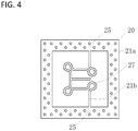
Fig. 4 is a schematic plan view showing another embodiment example in a main part of the wiring substrate of the present disclosure. -
Fig. 5 is a schematic plan view showing another embodiment example in a main part of the wiring substrate of the present disclosure. - Next, an example of an embodiment regarding the wiring substrate of the present disclosure will be described based on
Figs. 1 and2 .Fig. 1 is a schematic plan view from the side of third substrate that configures the wiring substrate of the present disclosure.Fig. 2 is a schematic sectional view passing between X and X shown inFig. 1 . - A
wiring substrate 1 includes afirst substrate 10, asecond substrate 20 and athird substrate 30. As shown inFig. 2 , in thewiring substrate 1, thesecond substrate 20 and thethird substrate 30 are sequentially stacked above thefirst substrate 10. - The
first substrate 10 and thethird substrate 30 may be, for instance, in the form of a flat plate. Thefirst substrate 10 and thethird substrate 30 have afirst antenna conductor 12 and asecond antenna conductor 32, respectively. A void is formed between thefirst substrate 10 and thethird substrate 30, for example, depending on the thickness of thesecond substrate 20. Thesecond substrate 20 has a shape including a frame body. - The
first substrate 10 includes, for instance, a firstinsulating layer 11, afirst antenna conductor 12, awiring conductor 13, afirst pad 14, anelectrode 15, and a solder resist 16. Thefirst substrate 10 is in a rectangular shape. Thefirst substrate 10, for example, has a length of 10 mm to 120 mm on one side and a thickness of 100 µm to 800 µm. - The first
insulating layer 11 includes, for instance, glass cloth and may also include at least one type of thermosetting resin, such as an epoxy resin or a bismaleimide triazine resin. - The first insulating
layer 11 is formed in the form of a flat plate by pressing a prepreg impregnated with a thermosetting resin such as an epoxy resin or a bismaleimide triazine resin in glass cloth under heat. - The first
insulating layer 11 has a plurality of throughholes 17 that penetrates between the upper surface (the side of the first antenna conductor 12) and the lower surface (the side of the electrode 15). The throughholes 17 have circular openings in plan view, for instance, on the upper and lower surfaces of the firstinsulating layer 11. The throughholes 17 are formed by drilling, blasting or laser machining, for instance. - A plurality of
first antenna conductors 12 is located on the upper surface of the firstinsulating layer 11, for example, spaced apart in the vertical and horizontal directions, respectively. The plurality offirst antenna conductors 12 opposes each of thesecond antenna conductors 32 on the surface of a thirdinsulating layer 31, as described later. - The
first antenna conductor 12 includes a metal, such as copper, for example. Thefirst antenna conductor 12 is formed using a plating technique such as a semi-additive or subtractive method. - The
wiring conductor 13 is located on the lower surface of the firstinsulating layer 11 and within the throughholes 17. A part of thewiring conductor 13 is connected to thefirst antenna conductor 12. - The
wiring conductor 13 includes a metal, such as copper, for instance. Thewiring conductor 13 is formed using a plating technique such as a semi-additive or subtractive method. - The
first pad 14 is located on the outer circumferential edge of the upper surface of the firstinsulating layer 11. Thefirst pad 14 includes a metal, such as copper, for example. Thefirst pad 14 is formed using a plating technique such as a semi-additive or subtractive method. - The
electrode 15 is located on the lower surface of the first insulating layer 11 (outermost surface of the wiring substrate 1). Theelectrode 15 is connected to the electrodes of an external electric substrate via solder. This allows thewiring substrate 1 to be electrically connected to the external electric substrate. Theelectrode 15 includes a metal, such as copper, for instance. Theelectrode 15 is formed by using a plating technique such as a semi-additive or subtractive method. Manufacturing efficiency is improved, when thefirst antenna conductor 12, thewiring conductor 13, thefirst pad 14 and theelectrode 15 are formed simultaneously by the above method. - The
solder resist 16 is located on a part of the upper and lower surfaces of the firstinsulating layer 11. Thesolder resist 16 has an opening 16a that exposes thefirst pad 14. Thesolder resist 16 has an opening 16b that exposes theelectrode 15. - The
solder resist 16 is formed in a predetermined pattern by applying, for example, a photosensitive thermosetting resin such as an acrylic-modified epoxy resin to the upper and lower surfaces of the firstinsulating layer 11 and exposing and developing the resin. - The
second substrate 20 is located on the upper surface of thefirst substrate 10. Thesecond substrate 20 includes a secondinsulating layer 21, asecond pad 22, athird pad 23, and a solder resist 24. - The second
insulating layer 21 includes, for instance, glass cloth, and also includes a thermosetting resin such as an epoxy resin or a bismaleimide triazine resin. The secondinsulating layer 21 has aframe body 21a and asupport body 21b. - The
frame body 21a is framed, for example, having a square inner and outer circumferences in plan view. The ends of thesupport body 21b are connected to two sides of theframe body 21a that are different from each other. The inside of theframe body 21a may be divided into a plurality of areas by thesupport body 21b. Theframe body 21a is located so as to protrude on the outer circumferential edge of thefirst substrate 10 in top view. - The
frame body 21a has two connectingparts 25 on the inner circumferential part and is connected to thesupport body 21b. The area surrounded by the inner circumferential part of theframe body 21a and thesupport body 21b is a void where the second insulatinglayer 21 does not exist. With thesecond substrate 20 interposed by thefirst substrate 10 and thethird substrate 30, this void constitutes thecavity 26. - The length of one side on the outer circumferential side of the
frame body 21a is, for instance, 20 mm to 150 mm, and the thickness is 50 µm to 1000 µm. The length of one side of theframe body 21a is preferably 3 mm to 10 mm larger than the length of one side of thefirst substrate 10. This allows the rigidity of theframe body 21a to be increased. When miniaturizing thewiring substrate 1, the length of one side of the frame body may be aligned with the length of one side of thefirst substrate 10. - The
support body 21b has a belt-like shape and connects the two connectingparts 25 to each other. Thesupport body 21b is located between thefirst antenna conductors 12 which are adjacent to each other in plan view. In plan view, there is no overlap between thesupport body 21b and thefirst antenna conductor 12. Thesupport body 21b has the function of a supporting part suppressing deformation of thefirst substrate 10 and thethird substrate 30 and preventing contact between thefirst substrate 10 and thethird substrate 30 in thewiring substrate 1. In the absence of thesupport body 21b, at least one of thefirst substrate 10 and thethird substrate 30 is deformed and enters the above void, resulting in contact between thefirst substrate 10 and thethird substrate 30. - As shown in
Fig. 1 , thesupport body 21b has fourdirection changing parts 27 between the two connectingparts 25. In the case of this example, thesupport body 21b is turned 90 degrees in thedirection changing part 27. Thesupport body 21b is not limited to a linear shape extending in one direction only. Thesupport body 21b can support thefirst substrate 10 and thethird substrate 30 in multiple directions. - The directions to be changed by the
direction changing part 27 are, for example, directions that intersect each other at 90 degrees. In the example shown inFig. 3 , onesupport body 21b includes a plurality ofdirection changing parts 27, each of which changes direction by 90 degrees. In the example shown inFig. 3 , the connectingpart 25 between thesupport body 21b and theframe body 21a is located at two side portions of thesquare frame body 21a that are opposed to each other. - In the example shown in
Fig. 3 , a closed shape (annular structure) is composed of theframe body 21a and thesupport body 21b in plan view. The annular structure in which thedirection changing part 27 is included on the circumference refers to, for instance, a closed structure such as a square shape configured only by thesupport body 21b. Thesupport body 21b does not have the annular structure in which thedirection changing part 27 is included on the circumference. This means that thesupport body 21b alone does not constitute the annular structure. - The
support body 21b has an elastic structure in which thedirection changing part 27 is a bending point between the connectingparts 25. As a result, when residual stresses during processing or thermal stresses due to heat dissipation of the electronic device are applied to thesupport body 21b, thedirection changing part 27 disperses the stresses. Therefore, it is possible to mitigate the deformation amount of thesupport body 21b and to suppress the deformation of thewiring substrate 1. - The
frame body 21a andsupport body 21b are formed, for example, by routing the second insulatinglayer 21 at positions corresponding to the inner circumference of theframe body 21a and the side of thesupport body 21b in the second insulatinglayer 21 and removing the second insulatinglayer 21. The width of theframe body 21a is, for instance, 0.5 mm to 10 mm. The width of thesupport body 21b is, for example, 0.5 mm to 5 mm. - The
second pad 22 opposes thefirst pad 14 at the outer circumferential edge of the lower surface of the second insulatinglayer 21. Thesecond pad 22 includes a metal, such as copper. Thesecond pad 22 is formed by using a plating technique such as a semi-additive or subtractive method. Thesecond pad 22 is connected to thefirst pad 14, for example, viasolder 28. Thereby, thesecond substrate 20 is fixed on thefirst substrate 10. Thefirst pad 14 and thesecond pad 22 may be physically or electrically connected to thefirst substrate 10 and thesecond substrate 20. - The
third pad 23 is located on the outer circumferential edge of the upper surface of the second insulatinglayer 21. Thethird pad 23 includes a metal, such as copper. Thethird pad 23 is formed by using a plating technique such as a semi-additive or subtractive method. The manufacturing efficiency is improved, when thesecond pad 22 and thethird pad 23 are formed simultaneously by the above method. - The solder resist 24 is located on a part of the upper and lower surface of the second insulating
layer 21. The solder resist 24 has anopening 24a that exposes thesecond pad 22. The solder resist 24 has anopening 24b that exposes thethird pad 23. - The
third substrate 30 is located on the upper surface of the second substrate 20 (the surface opposite to the first substrate 10) to cover the area (void) surrounded by the inner circumferential part of theframe body 21a and thesupport body 21b. As a result, thesecond substrate 20 is sandwiched between thefirst substrate 10 and thethird substrate 30, and the void constitutes thecavity 26. Thethird substrate 30 includes a third insulatinglayer 31, asecond antenna conductor 32, afourth pad 33, and a solder resist 34. - The third insulating
layer 31 includes, for example, glass cloth and includes a thermosetting resin such as an epoxy resin or a bismaleimide triazine resin. - The third insulating
layer 31 is formed in the form of a flat plate by pressing a prepreg impregnated with a thermosetting resin such as epoxy resin or bismaleimide triazine resin in glass cloth under heating. - The
second antenna conductor 32 is located on the upper surface (the surface opposite to the second substrate 20) and the lower surface (the surface on the side of the second substrate 20) of the third insulatinglayer 31, for example, spaced in the vertical and horizontal directions, respectively. In plan view, thesecond antenna conductor 32 overlaps the upper and lower surfaces of the third insulatinglayer 31. Thesecond antenna conductor 32 opposes thefirst antenna conductor 12 with the air layer in thecavity 26 interposed therebetween. In this example, the plurality ofsecond antenna conductors 32 on the upper surface of the third insulatinglayer 31, the plurality ofsecond antenna conductors 32 on the lower surface, and thefirst antenna conductor 12, which are opposed to each other, are formed with the same shape and the same size. - The
second antenna conductor 32 includes a metal, such as copper. Thesecond antenna conductor 32 is formed by using a plating technique such as a semi-additive or subtractive method. - The
fourth pad 33 is located opposite thethird pad 23 at the outer circumferential edge of the lower surface of the third insulatinglayer 31. Thefourth pad 33 includes a metal, such as copper. Thefourth pad 33 is formed by using a plating technique such as a semi-additive or subtractive method. Thefourth pad 33 is connected to thethird pad 23, for example, viasolder 28. As a result, thethird substrate 30 is fixed on thesecond substrate 20. - The
third pad 23 and thefourth pad 33 may be physically or electrically connected to thesecond substrate 20 and thethird substrate 30. For example, if thesecond substrate 20 is provided with a through hole conductor connecting to thesecond pad 22 and thethird pad 23, it is possible to electrically connect thefirst substrate 10, thesecond substrate 20 and thethird substrate 30, respectively. - The solder resist 34 is located on a part of the upper and lower surfaces of the third insulating
layer 31. The solder resist 34 has anopening 34a that exposes thefourth pad 33. - The
wiring substrate 1 used for such an antenna application has the following functions, for example. - First, the signal transmitted from the external electrical substrate is transmitted to the
first antenna conductor 12 via theelectrode 15 and thewiring conductor 13. - Next, the
first antenna conductor 12, which receives the signal supply, radiates the electromagnetic waves. - The electromagnetic waves then propagate through the air layer in the
cavity 26 to thesecond antenna conductor 32 on the lower surface side of the third insulatinglayer 31 and to thesecond antenna conductor 32 on the upper surface side. - The
second antenna conductor 32 on the upper surface side radiates electromagnetic waves to the outside. Alternatively, thesecond antenna conductor 32 has a function of transmitting electromagnetic waves received from the outside as a signal to the external electrical substrate by following the reverse route to the above. - For this reason, in the
wiring substrate 1, theframe body 21a andsupport body 21b, which constitute thecavity 26, are required to be located outside of the outer circumference of thefirst antenna conductor 12 to secure a path for the transmission and reception of electromagnetic waves. In thewiring substrate 1, the distance between thefirst antenna conductor 12 and thesecond antenna conductor 32 is maintained at a constant level to enable stable transmission and reception of electromagnetic waves between them. - The distance between the
first antenna conductor 12 and thesecond antenna conductor 32 can be adjusted to an optimum distance for sending and receiving electromagnetic waves for signals by adjusting the thickness of the second insulatinglayer 21. - The connection of the
first substrate 10, thesecond substrate 20 and thethird substrate 30 is performed, for example, as follows. - First, the
solder 28 is welded to at least one of thefirst pad 14 and thesecond pad 22, and at least one of thethird pad 23 and thefourth pad 33. - Next, the
second substrate 20 is placed on thefirst substrate 10 and thethird substrate 30 is placed on thesecond substrate 20, while thefirst pad 14 and thesecond pad 22 are facing each other as well as thethird pad 23 and thefourth pad 33. - Then, the
solder 28 is melted by the reflow treatment and cooled and fixed. This connects thefirst substrate 10, thesecond substrate 20 and thethird substrate 30 withsolder 28. - If it is desired to further ensure airtightness in the
cavity 26 or to improve the connection strength between thefirst substrate 10, thesecond substrate 20, and thethird substrate 30, a resin may be filled in the gap of the connection between thefirst substrate 10 and thesecond substrate 20 and the gap of the connection between thesecond substrate 20 and thethird substrate 30. - As shown in
Fig. 1 , in thewiring substrate 1 of the present disclosure, thesupport body 21b has fourdirection changing parts 27 between the two connectingparts 25, and does not have an annular structure where thedirection changing parts 27 are included on the circumference. - The
support body 21b has an elastic structure in which thedirection changing parts 27 are the bending points between the connectingparts 25. This allows the stresses to be dispersed to eachdirection changing parts 27, even if residual stresses during processing or thermal stresses due to heat dissipation of the electronics are applied to thesupport body 21b. Therefore, it is possible to mitigate the deformation amount of thesupport body 21b and to suppress the deformation of thewiring substrate 1. - As a result, for example, when the
wiring substrate 1 is used for an antenna application, it is possible to provide thewiring substrate 1 that enables stable transmission and reception of electromagnetic waves between thefirst antenna conductor 12 and thesecond antenna conductor 32 by maintaining a constant distance between them. - Although the wiring substrate in accordance with the embodiments of the present disclosure has been described above, it is not limited to an example of the above-described embodiments, and various improvements and modifications can be made within the scope of the claims. In
Figs. 1 and2 above, thesupport body 21b is shown in a linear shape, but as shown inFig. 3 , thedirection changing part 27 may have a curved shape. If thedirection changing part 27 has a curved shape, stresses are applied to the entire curved portion of thedirection changing part 27. As a result, the stresses can be dispersed and the damage to thedirection changing part 27 can be more suppressed. - As shown in
Fig. 4 , thedirection changing part 27 may have a bag shape. In this case, the stresses applied to thedirection changing part 27 can be more efficiently dispersed due to the elasticity of the bag-shaped portion. This makes it possible to better suppress the damage to thedirection changing part 27 due to large stresses. - For instance, if the
frame body 21a is a square frame shape having a pair of sides facing each other, as in each of the examples shown inFigs. 3 to 4 , the two connectingparts 25 may be located separately on a pair of sides of theframe body 21a. A plurality ofdirection changing parts 27 may be located between the two connectingparts 25. -
Fig. 5 is an example of a form having two connectingparts 25 located at the intersection of each other. In the above configuration, the deformation of thefirst substrate 10 and thethird substrate 30 between a pair of sides opposed to each other can be suppressed while maintaining sufficient void in theframe body 21a to function as an antenna. In other words, it is possible to make a wiring substrate for an antenna with excellent electromagnetic radiation characteristics. - In one example of the above-described embodiment, the connecting
parts 25 in theframe body 21a are located separately on a pair of opposing sides, but as shown inFig. 5 , the connectingparts 25 in theframe body 21a may be located separately on two opposing sides. In this case, the deformation amount of thewiring substrate 1 can be suppressed more evenly by thesupport body 21b, which is connected to the connectingparts 25 located on the two pairs of sides, respectively. - As described above, according to the wiring substrate of the present disclosure, a wiring substrate with small deformation can be provided. Therefore, it is effective for application to the wiring substrate that may be deformed by thermal stress caused by the heat dissipation of electronic devices. This is especially effective for application to the wiring substrate where many antenna circuits are located at high density due to the increased functionality and miniaturization of electronic devices and sensing devices.
- The present disclosure is not limited to the application of one example in the above embodiments. The wiring conductors for signal transmission may also be located.
-
- 1 Wiring Substrate
- 10 First Substrate
- 11 First Insulating Layer
- 12 First Antenna Conductor
- 13 Wiring Conductor
- 14 First Pad
- 15 Electrode
- 16 Solder Resist
- 16a, 16b Opening
- 17 Through hole
- 20 Second Substrate
- 21 Second Insulating Layer
- 21a Frame body
- 21b Support body
- 22 Second Pad
- 23 Third Pad
- 24 Solder Resist
- 24a, 24b Opening
- 25 Connecting part
- 26 Cavity
- 27 Direction Changing Part
- 28 Solder
- 30 Third Substrate
- 31 Third Insulating Layer
- 32 Second Antenna Conductor
- 33 Fourth Pad
- 34 Solder Resist
- 34a Opening
Claims (6)
- A wiring substrate comprising:a first substrate,a second substrate which is located on one side of the first substrate, comprising a frame body located on an outer circumferential edge of the first substrate, at least two connecting parts connected to an inner circumferential part of the frame body, and a support body connecting the two connecting parts to each other, anda third substrate which is located on a surface of the second substrate opposite to the first substrate,wherein the support body includes a direction changing part between the two connecting parts and does not include an annular structure where the direction changing part is included on the circumference.
- The wiring substrate according to Claim 1, wherein the direction changing part is in a curved shape.
- The wiring substrate according to Claim 1, wherein the direction changing part is in a bag shape.
- The wiring substrate according to any one of Claims 1 to 3,
wherein the frame body has a pair of sides facing each other,
the two connecting parts are located separately on the pair of sides of the frame body, and
a plurality of the direction changing parts is located between the two connecting parts. - The wiring substrate according to any one of Claims 1 to 4, wherein the first substrate, the second substrate, and the third substrate are electrically connected by an electrical conductor, respectively.
- The wiring substrate according to any one of Claims 1 to 5, wherein the second substrate includes a cavity surrounded by the inner circumferential part of the frame and the support body.
Applications Claiming Priority (2)
| Application Number | Priority Date | Filing Date | Title |
|---|---|---|---|
| JP2018053127 | 2018-03-20 | ||
| PCT/JP2019/002186 WO2019181187A1 (en) | 2018-03-20 | 2019-01-24 | Wiring substrate |
Publications (2)
| Publication Number | Publication Date |
|---|---|
| EP3771302A1 true EP3771302A1 (en) | 2021-01-27 |
| EP3771302A4 EP3771302A4 (en) | 2021-12-08 |
Family
ID=67986145
Family Applications (1)
| Application Number | Title | Priority Date | Filing Date |
|---|---|---|---|
| EP19771901.6A Withdrawn EP3771302A4 (en) | 2018-03-20 | 2019-01-24 | WIRING SUBSTRATE |
Country Status (6)
| Country | Link |
|---|---|
| US (1) | US11464104B2 (en) |
| EP (1) | EP3771302A4 (en) |
| JP (1) | JP7114690B2 (en) |
| CN (1) | CN111869337B (en) |
| TW (1) | TWI715922B (en) |
| WO (1) | WO2019181187A1 (en) |
Families Citing this family (2)
| Publication number | Priority date | Publication date | Assignee | Title |
|---|---|---|---|---|
| KR102766083B1 (en) * | 2019-04-12 | 2025-02-13 | 삼성전자 주식회사 | An antenna module including a printed circuit board and a base station including the antenna module |
| JP2023132708A (en) * | 2022-03-11 | 2023-09-22 | キオクシア株式会社 | Wiring boards and semiconductor devices |
Family Cites Families (23)
| Publication number | Priority date | Publication date | Assignee | Title |
|---|---|---|---|---|
| JPS63125003A (en) | 1986-11-15 | 1988-05-28 | Matsushita Electric Works Ltd | Plane antenna |
| JP3683422B2 (en) * | 1998-10-30 | 2005-08-17 | 三菱電機株式会社 | Microstrip antenna and microstrip antenna substrate |
| JP3888037B2 (en) * | 2000-06-20 | 2007-02-28 | セイコーエプソン株式会社 | Semiconductor device |
| TW521555B (en) * | 2000-08-25 | 2003-02-21 | Hitachi Aic Inc | Electronic device sealing electronic element therein and manufacturing method thereof, and printed wiring board suitable for such electronic device |
| KR101010789B1 (en) * | 2003-07-03 | 2011-01-25 | 르네사스 일렉트로닉스 가부시키가이샤 | Multi Function Card Device |
| TWI362231B (en) * | 2003-11-21 | 2012-04-11 | Semiconductor Energy Lab | Display device |
| JP2006211548A (en) * | 2005-01-31 | 2006-08-10 | Alps Electric Co Ltd | Nonreciprocal circuit element and transmission/reception module employing this nonreciprocal circuit element |
| US8472203B2 (en) * | 2007-09-04 | 2013-06-25 | Apple Inc. | Assembly of a handheld electronic device |
| US20130050227A1 (en) | 2011-08-30 | 2013-02-28 | Qualcomm Mems Technologies, Inc. | Glass as a substrate material and a final package for mems and ic devices |
| JP5927434B2 (en) * | 2011-09-30 | 2016-06-01 | パナソニックIpマネジメント株式会社 | Inertial force sensor |
| JP5922390B2 (en) * | 2011-12-13 | 2016-05-24 | 積水化学工業株式会社 | Spiral antenna for wireless power feeding |
| US20140048326A1 (en) * | 2012-08-14 | 2014-02-20 | Bridge Semiconductor Corporation | Multi-cavity wiring board for semiconductor assembly with internal electromagnetic shielding |
| US9130278B2 (en) * | 2012-11-26 | 2015-09-08 | Raytheon Company | Dual linear and circularly polarized patch radiator |
| JP6247106B2 (en) * | 2014-02-03 | 2017-12-13 | 新光電気工業株式会社 | Semiconductor device |
| US10444431B2 (en) * | 2015-01-15 | 2019-10-15 | National Institute Of Standards And Technology | Reticulated resonator, process for making and use of same |
| CN106796477B (en) * | 2015-02-27 | 2018-05-29 | 株式会社藤仓 | Wiring body, circuit board, Wiring structure body and touch sensor |
| JP6421077B2 (en) * | 2015-05-19 | 2018-11-07 | 富士フイルム株式会社 | Antenna manufacturing method and touch sensor |
| JP6591909B2 (en) * | 2015-07-27 | 2019-10-16 | 京セラ株式会社 | Antenna module |
| WO2017126596A1 (en) * | 2016-01-22 | 2017-07-27 | 京セラ株式会社 | Electronic component storage package, multi-piece wiring substrate, electronic device, and electronic module |
| JP6809876B2 (en) * | 2016-02-22 | 2021-01-06 | 京セラ株式会社 | Manufacturing method of wiring board, electronic device and wiring board |
| KR102351676B1 (en) * | 2017-06-07 | 2022-01-17 | 삼성전자주식회사 | A semiconductor package and a method for manufacturing the same |
| US20190082534A1 (en) * | 2017-09-08 | 2019-03-14 | Apple Inc. | Interconnect frames for sip modules |
| US11133591B2 (en) * | 2018-12-20 | 2021-09-28 | Sharp Kabushiki Kaisha | Antenna device, position input device including antenna device, and display device including antenna device |
-
2019
- 2019-01-24 US US16/981,312 patent/US11464104B2/en active Active
- 2019-01-24 JP JP2020507382A patent/JP7114690B2/en not_active Expired - Fee Related
- 2019-01-24 EP EP19771901.6A patent/EP3771302A4/en not_active Withdrawn
- 2019-01-24 WO PCT/JP2019/002186 patent/WO2019181187A1/en not_active Ceased
- 2019-01-24 CN CN201980019693.XA patent/CN111869337B/en active Active
- 2019-01-28 TW TW108103125A patent/TWI715922B/en active
Also Published As
| Publication number | Publication date |
|---|---|
| CN111869337B (en) | 2023-10-10 |
| WO2019181187A1 (en) | 2019-09-26 |
| JPWO2019181187A1 (en) | 2021-03-11 |
| EP3771302A4 (en) | 2021-12-08 |
| TWI715922B (en) | 2021-01-11 |
| US11464104B2 (en) | 2022-10-04 |
| TW201941381A (en) | 2019-10-16 |
| US20210014960A1 (en) | 2021-01-14 |
| CN111869337A (en) | 2020-10-30 |
| JP7114690B2 (en) | 2022-08-08 |
Similar Documents
| Publication | Publication Date | Title |
|---|---|---|
| EP4340012B1 (en) | Component carrier with integrated antenna arrangement, electronic apparatus, radio communication method | |
| CN113381190A (en) | Module comprising an antenna and an RF element and base station comprising a module | |
| EP3561955B1 (en) | Antenna substrate | |
| EP2785155B1 (en) | Circuit board and electronic device | |
| EP1127479B1 (en) | An electrical component and an electrical circuit module having connected ground planes | |
| US11464104B2 (en) | Wiring substrate | |
| JP6139585B2 (en) | High frequency module and microwave transceiver | |
| CN101488493A (en) | Package for electronic component and method for manufacturing the same | |
| KR20150138059A (en) | Wiring substrate | |
| KR102262073B1 (en) | Wiring substrate | |
| JP2021078003A (en) | Wireless module | |
| KR101924579B1 (en) | Stacked cable | |
| JP2019129249A (en) | Wiring board | |
| JP2024025972A (en) | Printed wiring boards and wireless communication terminals | |
| CN121772807A (en) | Electronic devices and their manufacturing methods, circuit boards, packaging modules and their manufacturing methods | |
| KR20200029324A (en) | Chip antenna module | |
| JP2020088202A (en) | Wiring board | |
| JP2006032595A (en) | Printed wiring board and electronic device |
Legal Events
| Date | Code | Title | Description |
|---|---|---|---|
| STAA | Information on the status of an ep patent application or granted ep patent |
Free format text: STATUS: THE INTERNATIONAL PUBLICATION HAS BEEN MADE |
|
| PUAI | Public reference made under article 153(3) epc to a published international application that has entered the european phase |
Free format text: ORIGINAL CODE: 0009012 |
|
| STAA | Information on the status of an ep patent application or granted ep patent |
Free format text: STATUS: REQUEST FOR EXAMINATION WAS MADE |
|
| 17P | Request for examination filed |
Effective date: 20200915 |
|
| AK | Designated contracting states |
Kind code of ref document: A1 Designated state(s): AL AT BE BG CH CY CZ DE DK EE ES FI FR GB GR HR HU IE IS IT LI LT LU LV MC MK MT NL NO PL PT RO RS SE SI SK SM TR |
|
| AX | Request for extension of the european patent |
Extension state: BA ME |
|
| DAV | Request for validation of the european patent (deleted) | ||
| DAX | Request for extension of the european patent (deleted) | ||
| A4 | Supplementary search report drawn up and despatched |
Effective date: 20211105 |
|
| RIC1 | Information provided on ipc code assigned before grant |
Ipc: H05K 1/02 20060101ALN20211101BHEP Ipc: H01Q 1/38 20060101ALI20211101BHEP Ipc: H05K 1/14 20060101AFI20211101BHEP |
|
| P01 | Opt-out of the competence of the unified patent court (upc) registered |
Effective date: 20230508 |
|
| STAA | Information on the status of an ep patent application or granted ep patent |
Free format text: STATUS: THE APPLICATION HAS BEEN WITHDRAWN |
|
| 18W | Application withdrawn |
Effective date: 20251009 |