EP3771196A1 - Camera module and optical device including same - Google Patents
Camera module and optical device including same Download PDFInfo
- Publication number
- EP3771196A1 EP3771196A1 EP19772457.8A EP19772457A EP3771196A1 EP 3771196 A1 EP3771196 A1 EP 3771196A1 EP 19772457 A EP19772457 A EP 19772457A EP 3771196 A1 EP3771196 A1 EP 3771196A1
- Authority
- EP
- European Patent Office
- Prior art keywords
- substrate
- circuit board
- printed circuit
- light
- case
- Prior art date
- Legal status (The legal status is an assumption and is not a legal conclusion. Google has not performed a legal analysis and makes no representation as to the accuracy of the status listed.)
- Granted
Links
Images



Classifications
-
- G—PHYSICS
- G03—PHOTOGRAPHY; CINEMATOGRAPHY; ANALOGOUS TECHNIQUES USING WAVES OTHER THAN OPTICAL WAVES; ELECTROGRAPHY; HOLOGRAPHY
- G03B—APPARATUS OR ARRANGEMENTS FOR TAKING PHOTOGRAPHS OR FOR PROJECTING OR VIEWING THEM; APPARATUS OR ARRANGEMENTS EMPLOYING ANALOGOUS TECHNIQUES USING WAVES OTHER THAN OPTICAL WAVES; ACCESSORIES THEREFOR
- G03B15/00—Special procedures for taking photographs; Apparatus therefor
- G03B15/02—Illuminating scene
- G03B15/03—Combinations of cameras with lighting apparatus; Flash units
-
- H—ELECTRICITY
- H05—ELECTRIC TECHNIQUES NOT OTHERWISE PROVIDED FOR
- H05K—PRINTED CIRCUITS; CASINGS OR CONSTRUCTIONAL DETAILS OF ELECTRIC APPARATUS; MANUFACTURE OF ASSEMBLAGES OF ELECTRICAL COMPONENTS
- H05K1/00—Printed circuits
- H05K1/18—Printed circuits structurally associated with non-printed electric components
-
- H—ELECTRICITY
- H05—ELECTRIC TECHNIQUES NOT OTHERWISE PROVIDED FOR
- H05K—PRINTED CIRCUITS; CASINGS OR CONSTRUCTIONAL DETAILS OF ELECTRIC APPARATUS; MANUFACTURE OF ASSEMBLAGES OF ELECTRICAL COMPONENTS
- H05K1/00—Printed circuits
- H05K1/18—Printed circuits structurally associated with non-printed electric components
- H05K1/181—Printed circuits structurally associated with non-printed electric components associated with surface mounted components
-
- H—ELECTRICITY
- H04—ELECTRIC COMMUNICATION TECHNIQUE
- H04N—PICTORIAL COMMUNICATION, e.g. TELEVISION
- H04N13/00—Stereoscopic video systems; Multi-view video systems; Details thereof
- H04N13/20—Image signal generators
- H04N13/204—Image signal generators using stereoscopic image cameras
- H04N13/254—Image signal generators using stereoscopic image cameras in combination with electromagnetic radiation sources for illuminating objects
-
- G—PHYSICS
- G02—OPTICS
- G02B—OPTICAL ELEMENTS, SYSTEMS OR APPARATUS
- G02B5/00—Optical elements other than lenses
- G02B5/02—Diffusing elements; Afocal elements
-
- G—PHYSICS
- G03—PHOTOGRAPHY; CINEMATOGRAPHY; ANALOGOUS TECHNIQUES USING WAVES OTHER THAN OPTICAL WAVES; ELECTROGRAPHY; HOLOGRAPHY
- G03B—APPARATUS OR ARRANGEMENTS FOR TAKING PHOTOGRAPHS OR FOR PROJECTING OR VIEWING THEM; APPARATUS OR ARRANGEMENTS EMPLOYING ANALOGOUS TECHNIQUES USING WAVES OTHER THAN OPTICAL WAVES; ACCESSORIES THEREFOR
- G03B30/00—Camera modules comprising integrated lens units and imaging units, specially adapted for being embedded in other devices, e.g. mobile phones or vehicles
-
- H—ELECTRICITY
- H04—ELECTRIC COMMUNICATION TECHNIQUE
- H04N—PICTORIAL COMMUNICATION, e.g. TELEVISION
- H04N13/00—Stereoscopic video systems; Multi-view video systems; Details thereof
- H04N13/20—Image signal generators
- H04N13/204—Image signal generators using stereoscopic image cameras
-
- H—ELECTRICITY
- H04—ELECTRIC COMMUNICATION TECHNIQUE
- H04N—PICTORIAL COMMUNICATION, e.g. TELEVISION
- H04N23/00—Cameras or camera modules comprising electronic image sensors; Control thereof
- H04N23/50—Constructional details
- H04N23/51—Housings
-
- H—ELECTRICITY
- H04—ELECTRIC COMMUNICATION TECHNIQUE
- H04N—PICTORIAL COMMUNICATION, e.g. TELEVISION
- H04N23/00—Cameras or camera modules comprising electronic image sensors; Control thereof
- H04N23/50—Constructional details
- H04N23/54—Mounting of pick-up tubes, electronic image sensors, deviation or focusing coils
-
- H—ELECTRICITY
- H04—ELECTRIC COMMUNICATION TECHNIQUE
- H04N—PICTORIAL COMMUNICATION, e.g. TELEVISION
- H04N23/00—Cameras or camera modules comprising electronic image sensors; Control thereof
- H04N23/50—Constructional details
- H04N23/55—Optical parts specially adapted for electronic image sensors; Mounting thereof
-
- H—ELECTRICITY
- H04—ELECTRIC COMMUNICATION TECHNIQUE
- H04N—PICTORIAL COMMUNICATION, e.g. TELEVISION
- H04N23/00—Cameras or camera modules comprising electronic image sensors; Control thereof
- H04N23/56—Cameras or camera modules comprising electronic image sensors; Control thereof provided with illuminating means
-
- H—ELECTRICITY
- H04—ELECTRIC COMMUNICATION TECHNIQUE
- H04N—PICTORIAL COMMUNICATION, e.g. TELEVISION
- H04N23/00—Cameras or camera modules comprising electronic image sensors; Control thereof
- H04N23/57—Mechanical or electrical details of cameras or camera modules specially adapted for being embedded in other devices
-
- H—ELECTRICITY
- H10—SEMICONDUCTOR DEVICES; ELECTRIC SOLID-STATE DEVICES NOT OTHERWISE PROVIDED FOR
- H10W—GENERIC PACKAGES, INTERCONNECTIONS, CONNECTORS OR OTHER CONSTRUCTIONAL DETAILS OF DEVICES COVERED BY CLASS H10
- H10W90/00—Package configurations
-
- H—ELECTRICITY
- H05—ELECTRIC TECHNIQUES NOT OTHERWISE PROVIDED FOR
- H05K—PRINTED CIRCUITS; CASINGS OR CONSTRUCTIONAL DETAILS OF ELECTRIC APPARATUS; MANUFACTURE OF ASSEMBLAGES OF ELECTRICAL COMPONENTS
- H05K2201/00—Indexing scheme relating to printed circuits covered by H05K1/00
- H05K2201/10—Details of components or other objects attached to or integrated in a printed circuit board
- H05K2201/10007—Types of components
- H05K2201/10106—Light emitting diode [LED]
-
- H—ELECTRICITY
- H05—ELECTRIC TECHNIQUES NOT OTHERWISE PROVIDED FOR
- H05K—PRINTED CIRCUITS; CASINGS OR CONSTRUCTIONAL DETAILS OF ELECTRIC APPARATUS; MANUFACTURE OF ASSEMBLAGES OF ELECTRICAL COMPONENTS
- H05K2201/00—Indexing scheme relating to printed circuits covered by H05K1/00
- H05K2201/10—Details of components or other objects attached to or integrated in a printed circuit board
- H05K2201/10007—Types of components
- H05K2201/10121—Optical component, e.g. opto-electronic component
-
- H—ELECTRICITY
- H05—ELECTRIC TECHNIQUES NOT OTHERWISE PROVIDED FOR
- H05K—PRINTED CIRCUITS; CASINGS OR CONSTRUCTIONAL DETAILS OF ELECTRIC APPARATUS; MANUFACTURE OF ASSEMBLAGES OF ELECTRICAL COMPONENTS
- H05K2201/00—Indexing scheme relating to printed circuits covered by H05K1/00
- H05K2201/10—Details of components or other objects attached to or integrated in a printed circuit board
- H05K2201/10007—Types of components
- H05K2201/10151—Sensor
-
- Y—GENERAL TAGGING OF NEW TECHNOLOGICAL DEVELOPMENTS; GENERAL TAGGING OF CROSS-SECTIONAL TECHNOLOGIES SPANNING OVER SEVERAL SECTIONS OF THE IPC; TECHNICAL SUBJECTS COVERED BY FORMER USPC CROSS-REFERENCE ART COLLECTIONS [XRACs] AND DIGESTS
- Y02—TECHNOLOGIES OR APPLICATIONS FOR MITIGATION OR ADAPTATION AGAINST CLIMATE CHANGE
- Y02P—CLIMATE CHANGE MITIGATION TECHNOLOGIES IN THE PRODUCTION OR PROCESSING OF GOODS
- Y02P70/00—Climate change mitigation technologies in the production process for final industrial or consumer products
- Y02P70/50—Manufacturing or production processes characterised by the final manufactured product
Definitions
- Embodiments relate to a camera module and an optical device.
- Methods of implementing a 3D stereoscopic image include a stereoscopic method, a time-of-flight (ToF) method, and a structured light method.
- the time-of-flight (ToF) method acquires depth information of an object by directly radiating light onto the object and calculating the time taken for the light to return after being reflected from the object.
- Embodiments include a camera module and an optical device including the same that are capable of facilitating a change in the design of a diffusion unit, preventing an increase in manufacturing costs attributable to the design change, preventing contamination or generation of foreign substances attributable to an SMT process, and preventing collision between a gripper of a wire-bonding apparatus and components to protect the components during wire bonding.
- a camera module may include a light emitter including a substrate and a light-emitting diode disposed on the substrate, a light receiver including a lens barrel and a sensor, a case accommodating the light emitter, a diffusion unit coupled to the case and disposed on the light emitter, a printed circuit board coupled to the substrate and the sensor, a first wire electrically connecting the light emitter to the substrate, and a second wire electrically connecting the substrate to the printed circuit board.
- the case may accommodate the light receiver.
- the case may be coupled to the printed circuit board, and the diffusion unit may be spaced apart from the light emitter.
- the substrate and the sensor may be attached to the upper surface of the printed circuit board.
- the camera module may further include a stiffener disposed under the printed circuit board and coupled to the printed circuit board, and the printed circuit board may include therein a first opening in which the substrate is disposed.
- the printed circuit board may include therein a second opening in which the sensor is disposed, and the sensor may be coupled to the stiffener.
- the case may include a first case accommodating the light emitter and a second case accommodating the light receiver.
- the first case and the second case may be spaced apart from each other.
- the diffusion unit may be coupled to the first case.
- the printed circuit board may include a first printed circuit board, disposed under the first case, and a second printed circuit board, disposed under the second case and spaced apart from the first printed circuit board.
- the substrate may be disposed on the first printed circuit board, and the sensor may be disposed on the second printed circuit board.
- the light emitter may include a sidewall disposed on the upper surface of the substrate and protruding from the substrate toward the diffusion unit, and the sidewall may have therein an opening that is open to one of sides of the upper surface of the substrate.
- the sidewall may include a first sidewall disposed adjacent to a first short side of the substrate and a second sidewall disposed adjacent to a second short side of the substrate, which is located opposite the first short side.
- the opening in the sidewall may be open to a first long side of the substrate, which is located between the first short side and the second short side.
- the height from the upper surface of the substrate to the upper end of the sidewall may be greater than the height to the upper surface of the light-emitting diode.
- Embodiments are capable of facilitating a change in the design of a diffusion unit, preventing an increase in manufacturing costs attributable to the design change, preventing contamination or generation of foreign substances attributable to an SMT process, and preventing collision between a gripper of a wire-bonding apparatus and components to protect the components during wire bonding.
- the embodiments will be described using the Cartesian coordinate system (x, y, z), but the embodiments are not limited thereto, and may be described using other coordinate systems.
- the x-axis and the y-axis may be directions perpendicular to the z-axis, which is an optical-axis direction
- the z-axis direction which is the optical-axis direction or a direction parallel to the optical axis
- the x-axis direction may be referred to as a 'second direction'
- the y-axis direction may be referred to as a 'third direction'.
- a camera module 1000 is a device capable of capturing a stereoscopic image using a time-of-flight (ToF) method, and may include a light transmitter configured to emit light to an object (or a target) and a light receiver configured to receive the light reflected from the object (or the target).
- ToF time-of-flight
- FIG. 1 is a cross-sectional view of the camera module 1000 according to an embodiment
- FIG. 2 is a plan view of the camera module 1000 of FIG. 1 .
- the camera module 1000 may include a light transmitter 100-1, a light receiver 100-2, and a case 100-3.
- the case 100-3 may be referred to as a housing or a holder.
- the light transmitter 100-1 radiates divergent light having a predetermined field of view to an object (or a target).
- the light transmitter 100-1 may include a light emitter 20 and a diffusion unit 30.
- the light emitter 20 may generate light.
- the light emitter 20 may generate infrared light or laser light.
- the light emitter 20 may include a substrate 10 and a light-emitting diode 22 disposed on the substrate 10.
- the light-emitting diode 22 may generate light in an infrared ray (IR) range.
- IR infrared ray
- the light-emitting diode 22 may be a laser diode.
- the light-emitting diode 22 may be a vertical cavity surface emitting laser (VCSEL).
- VCSEL vertical cavity surface emitting laser
- the light-emitting diode 22 may include a wafer and a plurality of light-emitting diodes disposed or arranged on the wafer.
- the light-emitting diodes may be arranged in a matrix form, without being limited thereto.
- the light emitter 20 may further include a photodiode 23 configured to sense light generated from the light-emitting diode 22.
- the performance of the light-emitting diode 22, or whether the light-emitting diode 22 is operating normally, may be determined based on the intensity of light from the light-emitting diode 22 sensed by the photodiode 23.
- the camera module 1000 may further include a controller (not shown) configured to determine, based on the intensity of light from the light-emitting diode 22 sensed by the photodiode 23, the performance of the light-emitting diode 22 or whether the light-emitting diode 22 is operating normally.
- a controller not shown
- the substrate 10 may be a substrate including metal for heat dissipation, for example, an aluminum or AlN substrate.
- the light-emitting diode 22 and the photodiode 23 may be attached to the substrate 10 using an adhesive member or a conductive adhesive (e.g. Ag epoxy).
- the diffusion unit 30 is disposed on the light-emitting diode 22, and diffuses light radiated from the light-emitting diode 22.
- the diffusion unit 30 may be a light diffusion unit.
- the diffusion unit 30 may be spaced apart from the light emitter 20, and may be opposite or aligned with the light-emitting diode 22 in a vertical direction.
- the diffusion unit 30 may convert or change the field of view of light radiated from the light emitter 20. That is, the diffusion unit 30 may change the light radiated from the light emitter 20 into divergent light forming a predetermined field of view.
- the diffusion unit 30 may include a diffusion member 32 and a housing 35 for accommodating the diffusion member 32.
- the diffusion member 32 may be made of a resin or plastic material including a light-diffusing agent and/or a light-scattering agent, without being limited thereto.
- the field of view of light radiated from the light emitter 20 may be 20 degrees to 40 degrees, and the field of view of light that has passed through the diffusion member 32 may be 60 degrees to 80 degrees.
- the diffusion member 32 may include at least one of a lens, a prism, a mirror, a diffuser, or a film.
- the lens may be a zoom lens or a liquid lens.
- the zoom lens may be moved in a forward-backward direction (or an upward-downward direction) on the axis of the divergent light, and the movement distance thereof may be adjusted to thereby change the field of view of the divergent light.
- the liquid lens may include two different types of liquids, which are disposed in a flat plate while forming an interface therebetween, and the curvature of the interface may change according to the magnitude of the driving voltage applied to both ends of the flat plate, with the result that the field of view of the divergent light may change.
- the diffusion member 32 may be disposed in the housing 35, and the housing 35 may be coupled to the top plate 101a of the case 100-3.
- the housing 35 and the case 100-3 may have a coupling structure (e.g. male-female coupling) so as to be coupled to each other.
- the coupling structure may be a protrusion or a groove, and the housing 35 may be fixed to or detachably mounted to the case 100-3.
- the housing 35 is provided separately from the case 100-3 and is coupled thereto, without being limited thereto.
- the housing 35 and the case 100-3 may be implemented in an integrated form.
- the case may be formed to have a protruding portion that protrudes from the top plate thereof so as to accommodate the diffusion member 32.
- the diffusion member 32 may include a lens unit and an optical path changing unit, which are sequentially arranged.
- the lens unit of the diffusion member 32 may include a collimator lens, and may convert the divergent light emitted from the light-emitting diode 22 into parallel light.
- the optical path changing unit of the diffusion member 32 may change the optical path of the parallel light that has passed through the lens unit of the diffusion member 32 so as to generate divergent light having a predetermined field of view.
- the optical path changing unit of the diffusion member 32 may include at least one of a prism, a lens, or a mirror.
- diffusion member 32 is merely given by way of example, and the diffusion member 32 may be implemented in various forms in order to radiate divergent light having a predetermined field of view onto an object.
- the housing 35 may include an opening formed therein to radiate light emitted from the diffusion member 32, and the diffusion unit 30 may further include a piece of glass mounted to the opening in the housing 35.
- the light receiver 100-2 may receive light reflected from an object (or a target).
- the reflected light may include light that originates from the light transmitter 100-1 and returns to the light receiver 100-2 via the target and light that originates from the sun or any other light source and enters the light receiver 100-2 via the target.
- the light receiver 100-2 may include a lens 105, a lens barrel 110 in which the lens 105 is mounted, a filter 120, and a sensor 130.
- the sensor 130 may be disposed below the lens 105, and may be an image sensor capable of converting light incident through the lens 105 into an electrical signal.
- the senor 130 may be implemented as a charge-coupled device or a complementary metal oxide semiconductor (CMOS).
- CMOS complementary metal oxide semiconductor
- the senor 130 may be an IR sensor or a time-of-flight (ToF) sensor.
- the sensor 130 may include an effective area 130a for sensing the light that has passed through the lens 105.
- the effective area 130a may be referred to as a light-receiving area, an active area, or a photographing area, and the center of the effective area 130a may correspond to or be aligned with the optical axis of the lens 105.
- the filter 120 may be disposed between the lens 105 and/or the lens barrel 110 and the sensor 130, and may serve to block light in a specific frequency band from entering the sensor 130 among the light passing through the lens.
- the filter 120 may be an IR pass filter, without being limited thereto. In another embodiment, the filter 120 may be an IR cutoff filter.
- the case 100-3 accommodates the light transmitter 100-1 and the light receiver 100-2 therein.
- the case 100-3 may be formed in the shape of a box that has an open bottom and includes a top plate 101a and side plates 101b, without being limited thereto.
- planar shape of the top plate 101a of the case 100-3 may be a polygon, such as a rectangle or an octagon, without being limited thereto.
- the top plate 101a of the case 100-3 may include therein a first opening 102a corresponding to the housing 35 of the diffusion unit 30 and a second opening 102b corresponding to the lens barrel 110 or the lens 105.
- each of the first opening 102a and the second opening 102b may have a rectangular shape or a circular shape.
- the housing 35 of the diffusion unit 30 may be coupled to the top plate 101a of the case 100-3.
- the housing 35 of the diffusion unit 30 may be coupled to the first opening 102a in the top plate 101a of the case 100-3, without being limited thereto.
- the housing 35 of the diffusion unit 30 may protrude in a forward or upward direction from the upper surface of the top plate 101a of the case 100-3.
- the forward or upward direction may be a direction oriented from the light emitter 20 to the diffusion unit 30.
- the lens barrel 110 may be coupled to the top plate 101a of the case 100-3.
- the lens barrel 110 may be disposed inside the second opening 102b in the top plate 101a of the case 100-3.
- the lens barrel 110 and/or the lens 105 may protrude in the forward or upward direction from the upper surface of the top plate 101a of the case 100-3.
- the camera module 1000 may further include a printed circuit board 140, which is disposed below the light-emitting diode 22 of the light emitter 20 and the lens barrel 110 and/or the lens 105 of the light receiver 100-2.
- the printed circuit board 140 may be disposed under the substrate 10 of the light emitter 20 and the sensor 130.
- the substrate 10 and the sensor 130 may be attached to the upper surface of the printed circuit board 140 using an adhesive member.
- the substrate 10 may be disposed in one region of the upper surface of the printed circuit board 140, and the sensor 130 may be disposed in another region of the upper surface of the printed circuit board 140.
- FIG. 3 is a plan view of the printed circuit board 140, the light emitter 20, and the sensor 130 of FIG. 1
- FIG. 4 is a cross-sectional view of the printed circuit board 140, the light emitter 20, and the sensor 130 shown in FIG. 3 when viewed in the direction AB.
- a wire 61 is not illustrated in FIG. 4 , which is a cross-sectional view taken in the direction AB of FIG. 3
- the light-emitting diode 22 is schematically illustrated in FIG. 4 in order to show the electrical connection between a first electrode 31 and a first terminal of the substrate 10.
- the light-emitting diode 22 may include a first electrode 31 and a second electrode (not shown).
- the photodiode 23 may include a first electrode 32 and a second electrode (not shown).
- the substrate 10 may include first and second terminals 51-1 and 51-2 and third and fourth terminals 52-1 and 52-2.
- the printed circuit board 140 may include first and second terminals 53-1 and 53-2 and third and fourth terminals 54-1 and 54-2.
- the light emitter 20 may further include a wire 61 connecting the first electrode 31 of the light-emitting diode 22 to the first terminal 51-1 of the substrate 10 and a wire 62-1 connecting the first terminal 51-1 of the substrate 10 to the first terminal 53-1 of the printed circuit board 140.
- the second electrode (not shown) of the light-emitting diode 22 may be electrically connected to the second terminal 51-2 of the substrate 10.
- the second electrode of the light-emitting diode 22 may be disposed on the lower surface of the light-emitting diode 22, a part of the second terminal 51-2 of the substrate 10 may be disposed under the second electrode of the light-emitting diode 22, and the second electrode of the light-emitting diode 22 and a part of the second terminal 51-2 of the substrate 10 may be electrically connected to each other using a conductive adhesive member.
- the light emitter 20 may further include a wire 62-2 connecting the second terminal 51-2 of the substrate 10 to the second terminal 53-2 of the printed circuit board 140. Accordingly, the light-emitting diode 22 may be electrically connected to the first and second terminals 53-1 and 53-2 of the printed circuit board 140.
- terminal may be replaced with “conductive layer”, “pad”, or “electrode”.
- electrode may be replaced with "pad” or "conductive layer”.
- the light emitter 20 may further include a wire 63 connecting the first electrode 32 of the photodiode 32 to the third terminal 52-1 of the substrate 10 and a wire 64-1 connecting the third terminal 52-1 of the substrate 10 to the third terminal 54-1 of the printed circuit board 140.
- the second electrode (not shown) of the photodiode 32 may be electrically connected to the fourth terminal 52-2 of the substrate 10.
- the second electrode of the photodiode 32 may be located on the lower surface of the photodiode, a part of the fourth terminal 52-2 of the substrate 10 may be located under the second electrode of the photodiode 32, and a part of the fourth terminal 52-2 of the substrate 10 and the fourth terminal 52-2 of the substrate 10 may be electrically connected to each other using a conductive adhesive member.
- the light emitter 20 may further include a wire 64-2 connecting the fourth terminal 52-2 of the substrate 10 to the fourth terminal 54-2 of the printed circuit board 140.
- the substrate 10 may have a rectangular shape, and the upper surface of the substrate 10 may include four sides.
- the upper surface of the substrate 10 may have two long sides facing each other and two short sides facing each other.
- the first terminal 51-1 of the substrate 10 may be disposed adjacent to the first long side of the upper surface of the substrate 10 and the first short side adjacent to the first long side, and may have an inverted L-shape, without being limited thereto.
- the second terminal 51-2 of the substrate 10 may be disposed adjacent to the first short side of the substrate 10, and may be positioned between the first terminal and the second long side of the substrate 10.
- the second long side of the substrate 10 may be the side that faces or is located opposite the first long side of the substrate 10.
- first and second terminals 53-1 and 53-2 of the printed circuit board 140 may be disposed adjacent to the first short side of the upper surface of the printed circuit board 140, which corresponds to the first short side of the substrate 10.
- the third terminal 52-1 of the substrate 10 may be disposed adjacent to the first long side of the substrate 10 and the second short side adjacent to the first long side.
- the third terminal 52-1 may be formed to bend from the first long side to the second short side of the substrate 10.
- the fourth terminal 52-2 of the substrate 10 may be disposed adjacent to the second short side of the substrate 10.
- the third terminal 54-1 and the fourth terminal 54-2 of the printed circuit board 140 may be disposed in the region of the upper surface of the printed circuit board 140 that is adjacent to the second short side of the substrate 10.
- the sensor 130 may include at least one electrode 33, and the printed circuit board 140 may further include a fifth terminal 55 to be electrically connected to the sensor 130.
- the light receiver 100-2 may further include a wire 65 connecting the electrode 33 of the sensor 130 to the fifth terminal 55 of the printed circuit board 140.
- the thickness of the substrate 10 may be greater than the thickness of the sensor 130. The reason for this is that, since the light emitter 22 and the photodiode 23 are mounted on the substrate 10 and a wire-bonding process is performed on the substrate 10, the substrate 10 needs to exhibit durability or strength capable of withstanding this process.
- the camera module 1000 may further include a stiffener disposed under the printed circuit board 140.
- the stiffener functions to support the printed circuit board 140 or to enhance the strength of the printed circuit board 140, and may be made of a metal material such as SUS.
- the stiffener may perform a heat dissipation function for dissipating the heat generated from the light source module and/or the sensor.
- FIG. 5 is a partial cross-sectional view of a camera module 1000-1 including a printed circuit board 140-1 and a stiffener 150 according to another embodiment.
- the camera module 1000-1 may include the diffusion unit 30, the lens 105, the lens barrel 110, the filter 120, and the case 100-3 of FIG. 1 , to which the description made with reference to FIGs. 1 to 4 may apply.
- the camera module 1000-1 may include a stiffener 150 disposed under the printed circuit board 140.
- the printed circuit board 140-1 may include therein a first opening 501 corresponding to the substrate 10 and a second opening 502 corresponding to the sensor 130.
- Each of the first opening 501 and the second opening 502 may be a through-hole penetrating the printed circuit board 140-1.
- the first opening 501 may have a shape corresponding to the substrate 10, for example, a rectangular shape
- the second opening 501 may have a shape corresponding to the sensor 130, for example, a rectangular shape.
- the area of the first opening 501 defined by the length thereof in the horizontal direction and the length thereof in the vertical direction may be greater than the area of the substrate 10 defined by the length thereof in the horizontal direction and the length thereof in the vertical direction (e.g. the area of the lower surface of the substrate 10).
- the area of the second opening 501 defined by the length thereof in the horizontal direction and the length thereof in the vertical direction may be greater than the area of the sensor 130 defined by the length thereof in the horizontal direction and the length thereof in the vertical direction (e.g. the area of the lower surface of the sensor).
- the stiffener 150 may include a first region S1, in which the printed circuit board 140-1 is disposed, a second region S2 corresponding to the first opening 501 in the printed circuit board 140-1, and a third region S3 corresponding to the second opening 502.
- the printed circuit board 140-1 may be attached or fixed to the upper surface of the stiffener 150, for example, the first region S1, using an adhesive member (not shown).
- the substrate 10 is disposed in the second region S2 of the stiffener 150.
- the substrate 10 may be attached or fixed to the second region S2 of the stiffener 150 using an adhesive member (not shown).
- the sensor 130 is disposed in the third region S3 of the stiffener 150.
- the sensor 130 may be attached or fixed to the third region S3 of the stiffener 130 using an adhesive member (not shown).
- the substrate 10 is disposed inside the first opening 501 in the printed circuit board 140-1 and the sensor 130 is disposed inside the second opening 502 in the printed circuit board 140-1, it is possible to reduce the height from the lower surface of the stiffener 150 to the upper surface of the light source module and/or the sensor, whereby the embodiment is capable of reducing the height of the camera module 1000-1.
- the substrate 10 is disposed inside the first opening 501 in the printed circuit board 140-1 and the sensor 130 is disposed inside the second opening 502 in the printed circuit board 140-1, it is possible to reduce the height difference between the upper surface of the substrate 10 and the upper surface of the printed circuit board 140-1 in the vertical direction and to reduce the height difference between the upper surface of the printed circuit board 140-1 and the sensor 130 in the vertical direction, whereby the embodiment is capable of enhancing the reliability of connection or bonding of the wires 62-1, 62-2, 64-1 and 64-2 between the substrate 10 and the printed circuit board 140-1 and enhancing the reliability of connection or bonding of the wire 65 between the sensor 130 and the printed circuit board 140-1.
- FIG. 6 is a cross-sectional view of a camera module 1000-2 according to another embodiment.
- the camera module 1000-2 may include a light transmitter 100-1a, a light receiver 100-1b, and a connection substrate 140c.
- the same reference numerals as those in FIG. 1 denote the same components, and a description of the same components will be omitted or made briefly.
- the light transmitter 100-1 and the light receiver 100-2 of FIG. 1 are mounted on one printed circuit board 140 and are accommodated in one case, the light transmitter 100-1a of FIG. 6 may be disposed or mounted on a first printed circuit board 140a, and the light receiver 100-2a of FIG. 6 may be disposed or mounted on a second printed circuit board 140b.
- the printed circuit board 140 of FIG. 1 may be divided into the first printed circuit board 140a and the second printed circuit board 140b of FIG. 6 , and the case 100-3 of FIG. 1 may be divided into the first case 100-3a and the second case 100-3b of FIG. 6 .
- the first case 100-3a may have therein a first opening 102a, and may accommodate the light emitter 20.
- the second case 100-3b may be spaced apart from the first case, may have therein a second opening 102b, and may accommodate a lens barrel 110 and a sensor 130.
- a diffusion unit 30 may be coupled to the first case 100-3a.
- the first printed circuit board 140a may be disposed under the first case 100-3a, and the second printed circuit board 140b may be spaced apart from the first printed circuit board 140a, and may be disposed under the second case 100-3b.
- the substrate 10 may be disposed on the first printed circuit board 140a, and the sensor 130 may be disposed on the second printed circuit board 140b.
- the light transmitter 100-1a may include a light emitter 20, a first printed circuit board 140a, a first case 100-3a, and a diffusion unit 30.
- the light emitter 20 may be disposed on the first printed circuit board 140a, and the diffusion unit 30 may be disposed in the first case 100-3a, and may be coupled to the first case 100-3a.
- the first case 100-3a may have therein a first opening corresponding to the diffusion unit 30.
- the description of the first opening 102a of FIG. 2 may apply to the first opening in the first case 100-3a.
- the description of the electrical connection relationships between the printed circuit board 140, the substrate 10, the light-emitting diode 22, and the photodiode 23 of FIGs. 3 and 4 may apply to the first printed circuit board 140a.
- the light receiver 100-2a may include a lens 105, a lens barrel 110, a filter 120, a sensor 130, a second printed circuit board 140b, and a second case 100-3b.
- the sensor 130 may be disposed on the second printed circuit board 140b, and the lens barrel 100 may be disposed in the second case 100-3b, and may be coupled to the second case 100-3b.
- the second case 100-3 may have therein a second opening corresponding to the lens barrel 105.
- the description of the second opening 102b of FIG. 2 may apply to the second opening in the second case 100-3b.
- the description of the electrical connection relationship between the printed circuit board 140 and the sensor 130 of FIGs. 3 and 4 may apply to the second printed circuit board 140b.
- the second case 100-3b may include therein a second opening, and may include a first holder 16a coupled to the lens barrel 110 and a second holder 16b disposed under the first holder 16a and configured to allow a filter to be mounted thereto.
- the lower end of the first holder 16a may be supported by the upper surface of the second holder 16b.
- the second holder 16b may be disposed on the second printed circuit board 140b, and may be provided in the lower surface thereof with a seating groove corresponding to the sensor 130.
- first holder 16a and the second holder 16b are provided separately from each other, without being limited thereto.
- first holder 16a and the second holder 16b may be integrated to form a single holder.
- connection substrate 140c connects the first printed circuit board 140a and the second printed circuit board 140b to each other.
- the connection substrate 140c may electrically connect the first printed circuit board 140a and the second printed circuit board 140b to each other.
- each of the first printed circuit board 140a and the second printed circuit board 140b may include at least one of a flexible PCB or a rigid PCB.
- the connection substrate 140c may be formed as a flexible PCB or a rigid-flexible PCB.
- the first printed circuit board 140a may have therein the first opening 501 of FIG. 5
- the second printed circuit board 140b may have therein the second opening 502 of FIG. 5
- the description of the printed circuit board 140-1 and the substrate 10 disposed on the stiffener 150 of FIG. 5 may apply to the first printed circuit board 140a and the stiffener according to another embodiment, and the description of the printed circuit board 140-1 and the sensor 130 disposed on the stiffener 150 of FIG. 5 may apply to the second printed circuit board 140b and the stiffener according to another embodiment.
- first printed circuit board 140a, the second printed circuit board 140b, and the connection substrate 140c may be integrated to form a single substrate.
- the camera module 1000 shown in FIG. 1 may be assembled in the following order.
- a chip-on-board (COB)-type light emitter 20 and a sensor 130 are prepared.
- the COB type refers to a structure in which a light-emitting diode (e.g. 22) and/or a photodiode 23 is disposed or mounted on a substrate 10.
- a light-emitting diode e.g. 22
- a photodiode 23 is disposed or mounted on a substrate 10.
- the light-emitting diode 22 and/or the photodiode 23 may be mounted or bonded to the substrate 10 using an insulating adhesive member or a conductive adhesive member (e.g. Ag epoxy).
- an insulating adhesive member e.g. Ag epoxy
- the light emitter 20 and the sensor 130 are mounted on a printed circuit board 140.
- the light emitter 20 and the sensor 130 may be attached or fixed to the printed circuit board 140 using an insulating adhesive member or a conductive adhesive member.
- wire bonding between the substrate 10 and the light-emitting diode 22 wire bonding between the substrate 10 and the printed circuit board 140, and wire bonding between the sensor 130 and the printed circuit board 140 are performed through soldering or surface mounter technology (SMT).
- SMT surface mounter technology
- a case 100-3 to which a lens 105, a diffusion unit 30, and a filter 120 are coupled, is attached to the printed circuit board 140.
- the lower portions or lower ends of the side plates of the case 100-3 may be coupled to the upper surface and/or the side surfaces of the printed circuit board 140.
- the top plate 101a of the case 100-3 may be located at a higher position than the upper surface of the light-emitting diode 22 and the upper surface of the photodiode 23, which are disposed on the substrate 10.
- the diffusion unit 30 may be disposed so as to be spaced apart from the light-emitting diode 22.
- a light source of a ToF-type camera module may be of a package type in which a light-emitting diode and a diffusion unit are packaged.
- a package-type light source in which the light-emitting diode and the diffusion unit are bonded to each other, the light-emitting diode and the diffusion unit are supplied in a packaged form. Therefore, upon change in field of illuminator (FOI), there may occur problems in which the package needs to be newly designed, the manufacturing costs thereof are therefore increased, previously manufactured packages remain unused, and delivery is delayed.
- FOI field of illuminator
- the light-emitting diode and the diffusion unit are bonded to each other using an adhesive member, and an air vent hole may be formed in the adhesive member in order to discharge gas generated in the process of mounting the package-type light-emitting diode to the substrate through SMT.
- a cleaning liquid may enter the air vent hole, thereby contaminating the light-emitting diode.
- the light-emitting diode 22 and the photodiode 23 are attached to the substrate 10, and the substrate 10 is attached to the printed circuit board using an adhesive, for example, epoxy, rather than SMT. Electrical connection between the light-emitting diode 22 and the substrate 10 and electrical connection between the substrate 10 and the printed circuit board 140 are realized through wire bonding.
- an adhesive for example, epoxy, rather than SMT.
- the diffusion unit 30 is coupled to the case 100-3, rather than being attached to the light emitter 20.
- FOI field of illuminator
- the diffusion unit 30 is changed in design and is mounted to the case 100-3, thereby preventing an increase in manufacturing costs attributable to the design change and preventing the occurrence of accumulated unused product and delayed delivery.
- the housing 140 having the diffusion unit 30 coupled thereto is coupled to the printed circuit board 140 in a clean room.
- the embodiment is capable of preventing contamination or generation of foreign substances, which may be caused by an SMT process, thus preventing a defect of the camera module due to foreign substances.
- FIG. 7 is a cross-sectional view of a camera module 1000-3 according to still another embodiment
- FIG. 8 is a plan view of the printed circuit board 140, the light emitter 20a, and the sensor 130 of FIG. 7
- FIG. 9 is a cross-sectional view of the printed circuit board 140, the light emitter 20a, and the sensor 130 shown in FIG. 8 when viewed in the direction AB.
- FIGs. 7 to 9 the same reference numerals as those in FIGs. 1 , 3 and 4 denote the same components, and a description of the same components will be made briefly or omitted.
- the camera module 1000-3 may include a light transmitter 100-1a, a light receiver 100-2, and a case 100-3.
- the light transmitter 100-1a may include a light emitter 20a and a diffusion unit 30.
- the light emitter 20a may include a substrate 10a and a light-emitting diode 22 disposed on the substrate 10a.
- the light emitter 20a may be of a type that is mounted on the printed circuit board 140 through an SMT process.
- the substrate 10a may be a substrate including metal for heat dissipation, for example, an aluminum or AlN substrate.
- the light-emitting diode 22 and a photodiode 23 may be attached to the substrate 10 using an adhesive member or a conductive adhesive (e.g. Ag epoxy).
- the substrate 10a may include a first terminal 51a to be connected to a first electrode 31 of the light-emitting diode 22, a second terminal (not shown) to be connected to a second electrode (not shown) of the light-emitting diode 22, a third terminal 52a to be connected to a first electrode 32 of the photodiode 23, and a fourth terminal (not shown) to be connected to a second electrode (not shown) of the photodiode 23.
- the first electrode 31 of the light-emitting diode 22 and the first terminal 51a of the substrate 10a may be electrically connected to each other via a wire 61a
- the second electrode of the light-emitting diode 22 and the second terminal of the substrate 10a may be electrically connected to each other using a conductive adhesive member (e.g. Ag epoxy).
- a conductive adhesive member e.g. Ag epoxy
- the first electrode 32 of the photodiode 23 and the third terminal 52a of the substrate 10a may be electrically connected to each other via a wire 63
- the second electrode of the photodiode 23 and the fourth terminal of the substrate 10a may be electrically connected to each other using a conductive adhesive member (e.g. Ag epoxy).
- a conductive adhesive member e.g. Ag epoxy
- the substrate 10a may include a first conductive layer and a second conductive layer, which are disposed on the lower surface of the substrate 10a, and may include a first connection electrode (not shown) for electrically connecting the first conductive layer to the second electrode (not shown) of the light-emitting diode 22 and a second connection electrode (not shown) for electrically connecting the second conductive layer to the second electrode of the photodiode 23.
- first connection electrode may electrically connect the second terminal of the substrate 10a to the first conductive layer
- second connection electrode may electrically connect the fourth terminal of the substrate 10a to the second conductive layer
- each of the first and second connection electrodes may be a via penetrating the substrate 10a or a contact via, without being limited thereto, and may be formed on the surface of the substrate 10a (at least one of the upper surface, the side surface, or the lower surface thereof).
- the light emitter 20a may be mounted on the printed circuit board 140 through an SMT process.
- the conductive layer of the substrate 10a of the light emitter 20a may be bonded to the printed circuit board 140 through an SMT process.
- the printed circuit board 140 is cleaned, and the sensor 130 is attached to the printed circuit board 140.
- wire bonding between the substrate 10a and the light-emitting diode 22 wire bonding between the substrate 10a and the printed circuit board 140, and wire bonding between the sensor 130 and the printed circuit board 140 are performed through soldering or surface mounter technology (SMT).
- SMT surface mounter technology
- the case 100-3 to which a lens 105, a diffusion unit 30, and a filter 120 are coupled, is attached to the printed circuit board 140.
- the lower portions or lower ends of the side plates of the case 100-3 may be coupled to the upper surface and/or the side surfaces of the printed circuit board 140.
- the light emitter 20a may include a sidewall 81 disposed on the upper surface of the substrate 10a.
- the sidewall 81 may have a shape protruding from the upper surface of the substrate 10a in the optical-axis direction or the vertical direction.
- the sidewall 81 may protrude or extend from the substrate 10a toward the diffusion unit 30.
- the sidewall 81 may prevent spatial interference between the gripper and the components 22, 23 and 130, thereby preventing the components 22, 23 and 130 from being damaged by the gripper.
- the sidewall 81 may include therein an opening that is open to one of the sides 71a to 71d of the upper surface of the substrate 10a.
- the sidewall 81 may include a first sidewall 10a disposed adjacent to the first short side 71a of the substrate 10a and a second sidewall 10b disposed adjacent to the second short side 71b of the substrate 10a.
- the second short side 71b may be a side that faces or is located opposite the first short side 71a.
- the opening in the sidewall 81 may be open to the first long side 71c of the substrate 10a, which is positioned between the first short side 71a and the second short side 71b.
- the sidewall 81 may include therein a first opening that is open to the first long side 71c of the substrate 10a and a second opening that is open to the second long side 71d of the substrate 10a.
- the sidewall 81 may not overlap the terminals 51a and 52a of the substrate 10a in the direction from the first long side 71c to the second long side 71d of the substrate 10a. That is, the sidewall may not be formed along the first long side 71c of the substrate 10a in order to facilitate wire bonding between the terminals 51a and 52a of the substrate 10a and the components 22 and 23.
- the height H from the upper surface of the substrate 10a to the upper end of the at least one sidewall 10a or 10b may be greater than the height to the upper surface of the light-emitting diode 22 and the height to the upper surface of the photodiode 23. The reason for this is to protect the components 22 and 23 from the gripper of the wire-bonding apparatus.
- the height H may be greater than the height to the highest point of the wire 61a formed between the light-emitting diode 22 and the terminal 51a of the substrate 10a and the height to the highest point of the wire 63 formed between the photodiode 23 and the terminal 52a of the substrate 10a.
- the sidewall 81 may further include a third sidewall (not shown) disposed adjacent to one of the first long side 71c and the second long side 71d of the substrate 10a.
- the height of the third sidewall may be the same as the heights of the first and second sidewalls.
- the sidewall 81 may be made of the same material as the substrate 10a, and may be integrally formed with the substrate 10a, without being limited thereto. In another embodiment, the sidewall 81 may be made of a material different from that of the substrate 10a, and may be attached to the substrate 10a using an adhesive member or the like, without being limited thereto.
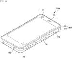
- FIG. 10 is a perspective view of a portable terminal 200A according to an embodiment
- FIG. 11 is a configuration diagram of the portable terminal 200A shown in FIG. 10 .
- the portable terminal 200A may include a body 850, a wireless communication unit 710, an A/V input unit 720, a sensor 740, an input/output unit 750, a memory 760, an interface 770, a controller 780, and a power supply 790.
- the body 850 shown in FIG. 10 has a bar shape, without being limited thereto, and may be any of various types such as, for example, a slide type, a folder type, a swing type, or a swivel type, in which two or more sub-bodies are coupled so as to be movable relative to each other.
- the body 850 may include a case (e.g. casing, housing, or cover) defining the external appearance thereof.
- the body 850 may be divided into a front case 851 and a rear case 852.
- a variety of electronic components of the terminal may be mounted in the space formed between the front case 851 and the rear case 852.
- the wireless communication unit 710 may include one or more modules, which enable wireless communication between the terminal 200A and a wireless communication system or between the terminal 200A and a network in which the terminal 200A is located.
- the wireless communication unit 710 may include a broadcast receiving module 711, a mobile communication module 712, a wireless Internet module 713, a nearfield communication module 714, and a location information module 715.
- the audio/video (A/V) input unit 720 serves to input audio signals or video signals, and may include a camera 721 and a microphone 722.
- the camera 721 may include the camera module 1000, 1000-1, 1000-2 or 1000-3 according to the embodiment shown in FIG. 1 , 5 , 6 or 7 .
- the sensor 740 may sense the current state of the terminal 200A, such as the open or closed state of the terminal 200A, the location of the terminal 200A, the presence or absence of a user's touch, the orientation of the terminal 200A, or the acceleration/deceleration of the terminal 200A, and may generate a sensing signal to control the operation of the terminal 200A. For example, when the terminal 200A is a slide-type phone, whether the slide-type phone is open or closed may be detected. In addition, the sensor 740 serves to sense whether power is supplied from the power supply 790 or whether the interface 770 is coupled to an external device.
- the input/output unit 750 serves to generate visual, audible, or tactile input or output.
- the input/output unit 750 may generate input data to control the operation of the terminal 200A, and may display information processed in the terminal 200A.
- the input/output unit 750 may include a keypad unit 730, a display panel 751, a sound output module 752, and a touchscreen panel 753.
- the keypad unit 730 may generate input data in response to input to a keypad.
- the display panel 751 may include a plurality of pixels, the color of which varies in response to electrical signals.
- the display panel 751 may include at least one of a liquid crystal display, a thin-film transistor liquid crystal display, an organic light-emitting diode, a flexible display, or a 3D display.
- the sound output module 752 may output audio data received from the wireless communication unit 710 in a call-signal reception mode, a call mode, a recording mode, a voice recognition mode, or a broadcast reception mode, or may output audio data stored in the memory 760.
- the touchscreen panel 753 may convert variation in capacitance, caused by a user's touch on a specific region of a touchscreen, into electrical input signals.
- the memory 760 may store programs for the processing and control of the controller 780, and may temporarily store input/output data (e.g. a phone book, messages, audio, still images, pictures, and moving images).
- input/output data e.g. a phone book, messages, audio, still images, pictures, and moving images.
- the memory 760 may store images captured by the camera 721, for example, pictures or moving images.
- the interface 770 serves as a passage for connection between the terminal 200A and an external device.
- the interface 770 may receive data or power from the external device, and may transmit the same to respective components inside the terminal 200A, or may transmit data inside the terminal 200A to the external device.
- the interface 770 may include a wired/wireless headset port, an external charger port, a wired/wireless data port, a memory card port, a port for connection of a device having an identification module, an audio input/output (I/O) port, a video input/output (I/O) port, and an earphone port.
- the controller 780 may control the general operation of the terminal 200A.
- the controller 780 may perform control and processing related to voice calls, data communication, and video calls.
- the controller 780 may include a multimedia module 781 for multimedia playback.
- the multimedia module 781 may be provided inside the controller 780, or may be provided separately from the controller 780.
- the controller 780 may perform pattern recognition processing, by which writing or drawing input to the touchscreen is perceived as characters or images.
- the power supply 790 may supply power required to operate the respective components upon receiving external power or internal power under the control of the controller 780.
- the controller 780 may analyze reflected light received by the sensor 130, and may acquire three-dimensional depth information of an object based on the result of analysis.
- the embodiments may be used in a camera module and an optical device including the same that are capable of facilitating a change in the design of a diffusion unit, preventing an increase in manufacturing costs attributable to the design change, preventing contamination or generation of foreign substances attributable to an SMT process, and preventing collision between a gripper of a wire-bonding apparatus and components to protect the components during wire bonding.
Landscapes
- Engineering & Computer Science (AREA)
- Multimedia (AREA)
- Signal Processing (AREA)
- Physics & Mathematics (AREA)
- General Physics & Mathematics (AREA)
- Microelectronics & Electronic Packaging (AREA)
- Electromagnetism (AREA)
- Optics & Photonics (AREA)
- Studio Devices (AREA)
- Camera Bodies And Camera Details Or Accessories (AREA)
- Lens Barrels (AREA)
- Stroboscope Apparatuses (AREA)
- Length Measuring Devices By Optical Means (AREA)
- Mechanical Light Control Or Optical Switches (AREA)
- Measurement Of Optical Distance (AREA)
Abstract
Description
- Embodiments relate to a camera module and an optical device.
- There have been developed mobile phones or smartphones equipped with a camera module that captures and stores an image or a video of an object. In addition, with increasing interest in stereoscopic service, camera modules providing a stereoscopic image have recently been developed.
- Methods of implementing a 3D stereoscopic image include a stereoscopic method, a time-of-flight (ToF) method, and a structured light method.
- The time-of-flight (ToF) method acquires depth information of an object by directly radiating light onto the object and calculating the time taken for the light to return after being reflected from the object.
- Embodiments include a camera module and an optical device including the same that are capable of facilitating a change in the design of a diffusion unit, preventing an increase in manufacturing costs attributable to the design change, preventing contamination or generation of foreign substances attributable to an SMT process, and preventing collision between a gripper of a wire-bonding apparatus and components to protect the components during wire bonding.
- A camera module according to an embodiment may include a light emitter including a substrate and a light-emitting diode disposed on the substrate, a light receiver including a lens barrel and a sensor, a case accommodating the light emitter, a diffusion unit coupled to the case and disposed on the light emitter, a printed circuit board coupled to the substrate and the sensor, a first wire electrically connecting the light emitter to the substrate, and a second wire electrically connecting the substrate to the printed circuit board.
- The case may accommodate the light receiver.
- The case may be coupled to the printed circuit board, and the diffusion unit may be spaced apart from the light emitter.
- The substrate and the sensor may be attached to the upper surface of the printed circuit board.
- The camera module may further include a stiffener disposed under the printed circuit board and coupled to the printed circuit board, and the printed circuit board may include therein a first opening in which the substrate is disposed.
- The printed circuit board may include therein a second opening in which the sensor is disposed, and the sensor may be coupled to the stiffener.
- The case may include a first case accommodating the light emitter and a second case accommodating the light receiver. The first case and the second case may be spaced apart from each other. The diffusion unit may be coupled to the first case. The printed circuit board may include a first printed circuit board, disposed under the first case, and a second printed circuit board, disposed under the second case and spaced apart from the first printed circuit board. The substrate may be disposed on the first printed circuit board, and the sensor may be disposed on the second printed circuit board.
- The light emitter may include a sidewall disposed on the upper surface of the substrate and protruding from the substrate toward the diffusion unit, and the sidewall may have therein an opening that is open to one of sides of the upper surface of the substrate.
- The sidewall may include a first sidewall disposed adjacent to a first short side of the substrate and a second sidewall disposed adjacent to a second short side of the substrate, which is located opposite the first short side. The opening in the sidewall may be open to a first long side of the substrate, which is located between the first short side and the second short side.
- The height from the upper surface of the substrate to the upper end of the sidewall may be greater than the height to the upper surface of the light-emitting diode.
- Embodiments are capable of facilitating a change in the design of a diffusion unit, preventing an increase in manufacturing costs attributable to the design change, preventing contamination or generation of foreign substances attributable to an SMT process, and preventing collision between a gripper of a wire-bonding apparatus and components to protect the components during wire bonding.
-
-
FIG. 1 is a cross-sectional view of a camera module according to an embodiment. -
FIG. 2 is a plan view of the camera module ofFIG. 1 . -
FIG. 3 is a plan view of the printed circuit board, the light emitter, and the sensor ofFIG. 1 . -
FIG. 4 is a cross-sectional view of the printed circuit board, the light emitter, and the sensor shown inFIG. 3 when viewed in the direction AB. -
FIG. 5 is a partial cross-sectional view of a camera module including a printed circuit board and a stiffener according to another embodiment. -
FIG. 6 is a cross-sectional view of a camera module according to another embodiment. -
FIG. 7 is a cross-sectional view of a camera module according to still another embodiment. -
FIG. 8 is a plan view of the printed circuit board, the substrate, the light emitter, the photodiode, and the sensor ofFIG. 7 . -
FIG. 9 is a cross-sectional view of the printed circuit board, the substrate, the light emitter, the photodiode, and the sensor shown inFIG. 8 when viewed in the direction AB. -
FIG. 10 is a perspective view of a portable terminal according to an embodiment. -
FIG. 11 is a configuration diagram of the portable terminal shown inFIG. 10 . - Hereinafter, embodiments of the present disclosure, which may concretely realize the objects described above, will be described with reference to the accompanying drawings.
- In the following description of the embodiments, it will be understood that, when each element is referred to as being "on" or "under" another element, it can be directly on or under the other element, or can be indirectly formed such that one or more intervening elements are also present. In addition, when an element is referred to as being "on or under", "under the element" as well as "on the element" may be included based on the element.
- In addition, the relational terms "first", "second", "on/upper part/above", and "under/lower part/below" are used herein only to distinguish between one subject or element and another subject or element without necessarily requiring or involving any physical or logical relationship or sequence between such subjects or elements. Wherever possible, the same reference numerals will be used throughout the drawings to refer to the same parts.
- Additionally, the terms "comprises", "includes", and "has" described herein should be interpreted not to exclude other elements but to further include such other elements, since the corresponding elements may be inherent unless mentioned otherwise. In addition, the term "corresponding to" herein may encompass at least one of the meanings of "facing" and "overlapping".
- For convenience of description, the embodiments will be described using the Cartesian coordinate system (x, y, z), but the embodiments are not limited thereto, and may be described using other coordinate systems. In the respective drawings, the x-axis and the y-axis may be directions perpendicular to the z-axis, which is an optical-axis direction, the z-axis direction, which is the optical-axis direction or a direction parallel to the optical axis, may be referred to as a 'first direction', the x-axis direction may be referred to as a 'second direction', and the y-axis direction may be referred to as a 'third direction'.
- A
camera module 1000 according to an embodiment is a device capable of capturing a stereoscopic image using a time-of-flight (ToF) method, and may include a light transmitter configured to emit light to an object (or a target) and a light receiver configured to receive the light reflected from the object (or the target). -
FIG. 1 is a cross-sectional view of thecamera module 1000 according to an embodiment, andFIG. 2 is a plan view of thecamera module 1000 ofFIG. 1 . - Referring to
FIGs. 1 and 2 , thecamera module 1000 may include a light transmitter 100-1, a light receiver 100-2, and a case 100-3. Here, the case 100-3 may be referred to as a housing or a holder. - The light transmitter 100-1 radiates divergent light having a predetermined field of view to an object (or a target).
- The light transmitter 100-1 may include a
light emitter 20 and adiffusion unit 30. - The
light emitter 20 may generate light. For example, thelight emitter 20 may generate infrared light or laser light. - For example, the
light emitter 20 may include asubstrate 10 and a light-emitting diode 22 disposed on thesubstrate 10. - For example, the light-
emitting diode 22 may generate light in an infrared ray (IR) range. - For example, the light-emitting
diode 22 may be a laser diode. - For example, the light-emitting
diode 22 may be a vertical cavity surface emitting laser (VCSEL). - For example, the light-emitting
diode 22 may include a wafer and a plurality of light-emitting diodes disposed or arranged on the wafer. In this case, the light-emitting diodes may be arranged in a matrix form, without being limited thereto. - The
light emitter 20 may further include aphotodiode 23 configured to sense light generated from the light-emitting diode 22. The performance of the light-emitting diode 22, or whether the light-emittingdiode 22 is operating normally, may be determined based on the intensity of light from the light-emittingdiode 22 sensed by thephotodiode 23. - For example, the
camera module 1000 may further include a controller (not shown) configured to determine, based on the intensity of light from the light-emittingdiode 22 sensed by thephotodiode 23, the performance of the light-emittingdiode 22 or whether the light-emittingdiode 22 is operating normally. - The
substrate 10 may be a substrate including metal for heat dissipation, for example, an aluminum or AlN substrate. The light-emittingdiode 22 and thephotodiode 23 may be attached to thesubstrate 10 using an adhesive member or a conductive adhesive (e.g. Ag epoxy). - The
diffusion unit 30 is disposed on the light-emittingdiode 22, and diffuses light radiated from the light-emittingdiode 22. For example, thediffusion unit 30 may be a light diffusion unit. - The
diffusion unit 30 may be spaced apart from thelight emitter 20, and may be opposite or aligned with the light-emittingdiode 22 in a vertical direction. - The
diffusion unit 30 may convert or change the field of view of light radiated from thelight emitter 20. That is, thediffusion unit 30 may change the light radiated from thelight emitter 20 into divergent light forming a predetermined field of view. - The
diffusion unit 30 may include adiffusion member 32 and ahousing 35 for accommodating thediffusion member 32. - The
diffusion member 32 may be made of a resin or plastic material including a light-diffusing agent and/or a light-scattering agent, without being limited thereto. - For example, the field of view of light radiated from the
light emitter 20 may be 20 degrees to 40 degrees, and the field of view of light that has passed through thediffusion member 32 may be 60 degrees to 80 degrees. - The
diffusion member 32 according to another embodiment may include at least one of a lens, a prism, a mirror, a diffuser, or a film. For example, the lens may be a zoom lens or a liquid lens. Here, the zoom lens may be moved in a forward-backward direction (or an upward-downward direction) on the axis of the divergent light, and the movement distance thereof may be adjusted to thereby change the field of view of the divergent light. In addition, the liquid lens may include two different types of liquids, which are disposed in a flat plate while forming an interface therebetween, and the curvature of the interface may change according to the magnitude of the driving voltage applied to both ends of the flat plate, with the result that the field of view of the divergent light may change. - For example, the
diffusion member 32 may be disposed in thehousing 35, and thehousing 35 may be coupled to thetop plate 101a of the case 100-3. For example, thehousing 35 and the case 100-3 may have a coupling structure (e.g. male-female coupling) so as to be coupled to each other. For example, the coupling structure may be a protrusion or a groove, and thehousing 35 may be fixed to or detachably mounted to the case 100-3. - In
FIG. 1 , thehousing 35 is provided separately from the case 100-3 and is coupled thereto, without being limited thereto. In another embodiment, thehousing 35 and the case 100-3 may be implemented in an integrated form. For example, the case may be formed to have a protruding portion that protrudes from the top plate thereof so as to accommodate thediffusion member 32. - For example, the
diffusion member 32 may include a lens unit and an optical path changing unit, which are sequentially arranged. The lens unit of thediffusion member 32 may include a collimator lens, and may convert the divergent light emitted from the light-emittingdiode 22 into parallel light. - In addition, the optical path changing unit of the
diffusion member 32 may change the optical path of the parallel light that has passed through the lens unit of thediffusion member 32 so as to generate divergent light having a predetermined field of view. For example, the optical path changing unit of thediffusion member 32 may include at least one of a prism, a lens, or a mirror. - The above description of the
diffusion member 32 is merely given by way of example, and thediffusion member 32 may be implemented in various forms in order to radiate divergent light having a predetermined field of view onto an object. - The
housing 35 may include an opening formed therein to radiate light emitted from thediffusion member 32, and thediffusion unit 30 may further include a piece of glass mounted to the opening in thehousing 35. - The light receiver 100-2 may receive light reflected from an object (or a target). Here, the reflected light may include light that originates from the light transmitter 100-1 and returns to the light receiver 100-2 via the target and light that originates from the sun or any other light source and enters the light receiver 100-2 via the target.
- The light receiver 100-2 may include a
lens 105, alens barrel 110 in which thelens 105 is mounted, afilter 120, and asensor 130. - The
sensor 130 may be disposed below thelens 105, and may be an image sensor capable of converting light incident through thelens 105 into an electrical signal. - For example, the
sensor 130 may be implemented as a charge-coupled device or a complementary metal oxide semiconductor (CMOS). - Further, for example, the
sensor 130 may be an IR sensor or a time-of-flight (ToF) sensor. - The
sensor 130 may include aneffective area 130a for sensing the light that has passed through thelens 105. For example, theeffective area 130a may be referred to as a light-receiving area, an active area, or a photographing area, and the center of theeffective area 130a may correspond to or be aligned with the optical axis of thelens 105. - The
filter 120 may be disposed between thelens 105 and/or thelens barrel 110 and thesensor 130, and may serve to block light in a specific frequency band from entering thesensor 130 among the light passing through the lens. - For example, when the
sensor 130 is an IR sensor, thefilter 120 may be an IR pass filter, without being limited thereto. In another embodiment, thefilter 120 may be an IR cutoff filter. - The case 100-3 accommodates the light transmitter 100-1 and the light receiver 100-2 therein.
- For example, the case 100-3 may be formed in the shape of a box that has an open bottom and includes a
top plate 101a andside plates 101b, without being limited thereto. - For example, the planar shape of the
top plate 101a of the case 100-3 may be a polygon, such as a rectangle or an octagon, without being limited thereto. - The
top plate 101a of the case 100-3 may include therein afirst opening 102a corresponding to thehousing 35 of thediffusion unit 30 and asecond opening 102b corresponding to thelens barrel 110 or thelens 105. - For example, each of the
first opening 102a and thesecond opening 102b may have a rectangular shape or a circular shape. - The
housing 35 of thediffusion unit 30 may be coupled to thetop plate 101a of the case 100-3. - For example, the
housing 35 of thediffusion unit 30 may be coupled to thefirst opening 102a in thetop plate 101a of the case 100-3, without being limited thereto. - The
housing 35 of thediffusion unit 30 may protrude in a forward or upward direction from the upper surface of thetop plate 101a of the case 100-3. Here, the forward or upward direction may be a direction oriented from thelight emitter 20 to thediffusion unit 30. - The
lens barrel 110 may be coupled to thetop plate 101a of the case 100-3. - For example, the
lens barrel 110 may be disposed inside thesecond opening 102b in thetop plate 101a of the case 100-3. - The
lens barrel 110 and/or thelens 105 may protrude in the forward or upward direction from the upper surface of thetop plate 101a of the case 100-3. - The
camera module 1000 may further include a printedcircuit board 140, which is disposed below the light-emittingdiode 22 of thelight emitter 20 and thelens barrel 110 and/or thelens 105 of the light receiver 100-2. - For example, the printed
circuit board 140 may be disposed under thesubstrate 10 of thelight emitter 20 and thesensor 130. For example, thesubstrate 10 and thesensor 130 may be attached to the upper surface of the printedcircuit board 140 using an adhesive member. - The
substrate 10 may be disposed in one region of the upper surface of the printedcircuit board 140, and thesensor 130 may be disposed in another region of the upper surface of the printedcircuit board 140. -
FIG. 3 is a plan view of the printedcircuit board 140, thelight emitter 20, and thesensor 130 ofFIG. 1 , andFIG. 4 is a cross-sectional view of the printedcircuit board 140, thelight emitter 20, and thesensor 130 shown inFIG. 3 when viewed in the direction AB. Awire 61 is not illustrated inFIG. 4 , which is a cross-sectional view taken in the direction AB ofFIG. 3 , and the light-emittingdiode 22 is schematically illustrated inFIG. 4 in order to show the electrical connection between afirst electrode 31 and a first terminal of thesubstrate 10. - Referring to
FIGs. 3 and 4 , the light-emittingdiode 22 may include afirst electrode 31 and a second electrode (not shown). Thephotodiode 23 may include afirst electrode 32 and a second electrode (not shown). - The
substrate 10 may include first and second terminals 51-1 and 51-2 and third and fourth terminals 52-1 and 52-2. - The printed
circuit board 140 may include first and second terminals 53-1 and 53-2 and third and fourth terminals 54-1 and 54-2. - The
light emitter 20 may further include awire 61 connecting thefirst electrode 31 of the light-emittingdiode 22 to the first terminal 51-1 of thesubstrate 10 and a wire 62-1 connecting the first terminal 51-1 of thesubstrate 10 to the first terminal 53-1 of the printedcircuit board 140. - In addition, the second electrode (not shown) of the light-emitting
diode 22 may be electrically connected to the second terminal 51-2 of thesubstrate 10. - For example, the second electrode of the light-emitting
diode 22 may be disposed on the lower surface of the light-emittingdiode 22, a part of the second terminal 51-2 of thesubstrate 10 may be disposed under the second electrode of the light-emittingdiode 22, and the second electrode of the light-emittingdiode 22 and a part of the second terminal 51-2 of thesubstrate 10 may be electrically connected to each other using a conductive adhesive member. - The
light emitter 20 may further include a wire 62-2 connecting the second terminal 51-2 of thesubstrate 10 to the second terminal 53-2 of the printedcircuit board 140. Accordingly, the light-emittingdiode 22 may be electrically connected to the first and second terminals 53-1 and 53-2 of the printedcircuit board 140. - Here, in the
substrate 10 or the printedcircuit board 140, the term "terminal" may be replaced with "conductive layer", "pad", or "electrode". In addition, in the light-emittingdiode 22 or thephotodiode 23, the term "electrode" may be replaced with "pad" or "conductive layer". - In addition, the
light emitter 20 may further include awire 63 connecting thefirst electrode 32 of thephotodiode 32 to the third terminal 52-1 of thesubstrate 10 and a wire 64-1 connecting the third terminal 52-1 of thesubstrate 10 to the third terminal 54-1 of the printedcircuit board 140. - The second electrode (not shown) of the
photodiode 32 may be electrically connected to the fourth terminal 52-2 of thesubstrate 10. For example, the second electrode of thephotodiode 32 may be located on the lower surface of the photodiode, a part of the fourth terminal 52-2 of thesubstrate 10 may be located under the second electrode of thephotodiode 32, and a part of the fourth terminal 52-2 of thesubstrate 10 and the fourth terminal 52-2 of thesubstrate 10 may be electrically connected to each other using a conductive adhesive member. - The
light emitter 20 may further include a wire 64-2 connecting the fourth terminal 52-2 of thesubstrate 10 to the fourth terminal 54-2 of the printedcircuit board 140. - For example, the
substrate 10 may have a rectangular shape, and the upper surface of thesubstrate 10 may include four sides. For example, the upper surface of thesubstrate 10 may have two long sides facing each other and two short sides facing each other. - For example, the first terminal 51-1 of the
substrate 10 may be disposed adjacent to the first long side of the upper surface of thesubstrate 10 and the first short side adjacent to the first long side, and may have an inverted L-shape, without being limited thereto. - In addition, for example, the second terminal 51-2 of the
substrate 10 may be disposed adjacent to the first short side of thesubstrate 10, and may be positioned between the first terminal and the second long side of thesubstrate 10. The second long side of thesubstrate 10 may be the side that faces or is located opposite the first long side of thesubstrate 10. - For example, the first and second terminals 53-1 and 53-2 of the printed
circuit board 140 may be disposed adjacent to the first short side of the upper surface of the printedcircuit board 140, which corresponds to the first short side of thesubstrate 10. - For example, the third terminal 52-1 of the
substrate 10 may be disposed adjacent to the first long side of thesubstrate 10 and the second short side adjacent to the first long side. The third terminal 52-1 may be formed to bend from the first long side to the second short side of thesubstrate 10. - For example, the fourth terminal 52-2 of the
substrate 10 may be disposed adjacent to the second short side of thesubstrate 10. - The third terminal 54-1 and the fourth terminal 54-2 of the printed
circuit board 140 may be disposed in the region of the upper surface of the printedcircuit board 140 that is adjacent to the second short side of thesubstrate 10. - The
sensor 130 may include at least oneelectrode 33, and the printedcircuit board 140 may further include afifth terminal 55 to be electrically connected to thesensor 130. - The light receiver 100-2 may further include a
wire 65 connecting theelectrode 33 of thesensor 130 to thefifth terminal 55 of the printedcircuit board 140. - The thickness of the
substrate 10 may be greater than the thickness of thesensor 130. The reason for this is that, since thelight emitter 22 and thephotodiode 23 are mounted on thesubstrate 10 and a wire-bonding process is performed on thesubstrate 10, thesubstrate 10 needs to exhibit durability or strength capable of withstanding this process. - Although not shown in
FIG. 3 , thecamera module 1000 may further include a stiffener disposed under the printedcircuit board 140. In this case, the stiffener functions to support the printedcircuit board 140 or to enhance the strength of the printedcircuit board 140, and may be made of a metal material such as SUS. In addition, the stiffener may perform a heat dissipation function for dissipating the heat generated from the light source module and/or the sensor. -
FIG. 5 is a partial cross-sectional view of a camera module 1000-1 including a printed circuit board 140-1 and astiffener 150 according to another embodiment. The camera module 1000-1 may include thediffusion unit 30, thelens 105, thelens barrel 110, thefilter 120, and the case 100-3 ofFIG. 1 , to which the description made with reference toFIGs. 1 to 4 may apply. - Referring to
FIG. 5 , the camera module 1000-1 may include astiffener 150 disposed under the printedcircuit board 140. - The printed circuit board 140-1 may include therein a
first opening 501 corresponding to thesubstrate 10 and asecond opening 502 corresponding to thesensor 130. - Each of the
first opening 501 and thesecond opening 502 may be a through-hole penetrating the printed circuit board 140-1. - The
first opening 501 may have a shape corresponding to thesubstrate 10, for example, a rectangular shape, and thesecond opening 501 may have a shape corresponding to thesensor 130, for example, a rectangular shape. - For example, the area of the
first opening 501 defined by the length thereof in the horizontal direction and the length thereof in the vertical direction may be greater than the area of thesubstrate 10 defined by the length thereof in the horizontal direction and the length thereof in the vertical direction (e.g. the area of the lower surface of the substrate 10). - In addition, the area of the
second opening 501 defined by the length thereof in the horizontal direction and the length thereof in the vertical direction may be greater than the area of thesensor 130 defined by the length thereof in the horizontal direction and the length thereof in the vertical direction (e.g. the area of the lower surface of the sensor). - The
stiffener 150 may include a first region S1, in which the printed circuit board 140-1 is disposed, a second region S2 corresponding to thefirst opening 501 in the printed circuit board 140-1, and a third region S3 corresponding to thesecond opening 502. - The printed circuit board 140-1 may be attached or fixed to the upper surface of the
stiffener 150, for example, the first region S1, using an adhesive member (not shown). - The
substrate 10 is disposed in the second region S2 of thestiffener 150. For example, thesubstrate 10 may be attached or fixed to the second region S2 of thestiffener 150 using an adhesive member (not shown). - The
sensor 130 is disposed in the third region S3 of thestiffener 150. For example, thesensor 130 may be attached or fixed to the third region S3 of thestiffener 130 using an adhesive member (not shown). - Since the
substrate 10 is disposed inside thefirst opening 501 in the printed circuit board 140-1 and thesensor 130 is disposed inside thesecond opening 502 in the printed circuit board 140-1, it is possible to reduce the height from the lower surface of thestiffener 150 to the upper surface of the light source module and/or the sensor, whereby the embodiment is capable of reducing the height of the camera module 1000-1. - In addition, since the
substrate 10 is disposed inside thefirst opening 501 in the printed circuit board 140-1 and thesensor 130 is disposed inside thesecond opening 502 in the printed circuit board 140-1, it is possible to reduce the height difference between the upper surface of thesubstrate 10 and the upper surface of the printed circuit board 140-1 in the vertical direction and to reduce the height difference between the upper surface of the printed circuit board 140-1 and thesensor 130 in the vertical direction, whereby the embodiment is capable of enhancing the reliability of connection or bonding of the wires 62-1, 62-2, 64-1 and 64-2 between thesubstrate 10 and the printed circuit board 140-1 and enhancing the reliability of connection or bonding of thewire 65 between thesensor 130 and the printed circuit board 140-1. -
FIG. 6 is a cross-sectional view of a camera module 1000-2 according to another embodiment. - Referring to
FIG. 6 , the camera module 1000-2 may include a light transmitter 100-1a, a light receiver 100-1b, and aconnection substrate 140c. The same reference numerals as those inFIG. 1 denote the same components, and a description of the same components will be omitted or made briefly. - While the light transmitter 100-1 and the light receiver 100-2 of
FIG. 1 are mounted on one printedcircuit board 140 and are accommodated in one case, the light transmitter 100-1a ofFIG. 6 may be disposed or mounted on a first printedcircuit board 140a, and the light receiver 100-2a ofFIG. 6 may be disposed or mounted on a second printedcircuit board 140b. - The printed
circuit board 140 ofFIG. 1 may be divided into the first printedcircuit board 140a and the second printedcircuit board 140b ofFIG. 6 , and the case 100-3 ofFIG. 1 may be divided into the first case 100-3a and the second case 100-3b ofFIG. 6 . - For example, the first case 100-3a may have therein a
first opening 102a, and may accommodate thelight emitter 20. The second case 100-3b may be spaced apart from the first case, may have therein asecond opening 102b, and may accommodate alens barrel 110 and asensor 130. - For example, a
diffusion unit 30 may be coupled to the first case 100-3a. - The first printed
circuit board 140a may be disposed under the first case 100-3a, and the second printedcircuit board 140b may be spaced apart from the first printedcircuit board 140a, and may be disposed under the second case 100-3b. - The
substrate 10 may be disposed on the first printedcircuit board 140a, and thesensor 130 may be disposed on the second printedcircuit board 140b. - The light transmitter 100-1a may include a
light emitter 20, a first printedcircuit board 140a, a first case 100-3a, and adiffusion unit 30. - The
light emitter 20 may be disposed on the first printedcircuit board 140a, and thediffusion unit 30 may be disposed in the first case 100-3a, and may be coupled to the first case 100-3a. - The first case 100-3a may have therein a first opening corresponding to the
diffusion unit 30. - The description of the
first opening 102a ofFIG. 2 may apply to the first opening in the first case 100-3a. The description of the electrical connection relationships between the printedcircuit board 140, thesubstrate 10, the light-emittingdiode 22, and thephotodiode 23 ofFIGs. 3 and 4 may apply to the first printedcircuit board 140a. - The light receiver 100-2a may include a
lens 105, alens barrel 110, afilter 120, asensor 130, a second printedcircuit board 140b, and a second case 100-3b. - The
sensor 130 may be disposed on the second printedcircuit board 140b, and the lens barrel 100 may be disposed in the second case 100-3b, and may be coupled to the second case 100-3b. - The second case 100-3 may have therein a second opening corresponding to the
lens barrel 105. The description of thesecond opening 102b ofFIG. 2 may apply to the second opening in the second case 100-3b. The description of the electrical connection relationship between the printedcircuit board 140 and thesensor 130 ofFIGs. 3 and 4 may apply to the second printedcircuit board 140b. - For example, the second case 100-3b may include therein a second opening, and may include a
first holder 16a coupled to thelens barrel 110 and asecond holder 16b disposed under thefirst holder 16a and configured to allow a filter to be mounted thereto. - The lower end of the
first holder 16a may be supported by the upper surface of thesecond holder 16b. - The
second holder 16b may be disposed on the second printedcircuit board 140b, and may be provided in the lower surface thereof with a seating groove corresponding to thesensor 130. - In
FIG. 6 , thefirst holder 16a and thesecond holder 16b are provided separately from each other, without being limited thereto. In another embodiment, thefirst holder 16a and thesecond holder 16b may be integrated to form a single holder. - The
connection substrate 140c connects the first printedcircuit board 140a and the second printedcircuit board 140b to each other. For example, theconnection substrate 140c may electrically connect the first printedcircuit board 140a and the second printedcircuit board 140b to each other. - For example, each of the first printed
circuit board 140a and the second printedcircuit board 140b may include at least one of a flexible PCB or a rigid PCB. Theconnection substrate 140c may be formed as a flexible PCB or a rigid-flexible PCB. - In the camera module according to another embodiment, the first printed
circuit board 140a may have therein thefirst opening 501 ofFIG. 5 , and the second printedcircuit board 140b may have therein thesecond opening 502 ofFIG. 5 , and may further include a first stiffener (not shown) disposed under the first printedcircuit board 140a and a second stiffener disposed under the second printedcircuit board 140b. - The description of the printed circuit board 140-1 and the
substrate 10 disposed on thestiffener 150 ofFIG. 5 may apply to the first printedcircuit board 140a and the stiffener according to another embodiment, and the description of the printed circuit board 140-1 and thesensor 130 disposed on thestiffener 150 ofFIG. 5 may apply to the second printedcircuit board 140b and the stiffener according to another embodiment. - Further, in another embodiment, the first printed
circuit board 140a, the second printedcircuit board 140b, and theconnection substrate 140c may be integrated to form a single substrate. - The
camera module 1000 shown inFIG. 1 may be assembled in the following order. - First, a chip-on-board (COB)-
type light emitter 20 and asensor 130 are prepared. - Here, the COB type refers to a structure in which a light-emitting diode (e.g. 22) and/or a
photodiode 23 is disposed or mounted on asubstrate 10. - For example, the light-emitting
diode 22 and/or thephotodiode 23 may be mounted or bonded to thesubstrate 10 using an insulating adhesive member or a conductive adhesive member (e.g. Ag epoxy). - Subsequently, the
light emitter 20 and thesensor 130 are mounted on a printedcircuit board 140. - For example, the
light emitter 20 and thesensor 130 may be attached or fixed to the printedcircuit board 140 using an insulating adhesive member or a conductive adhesive member. - Subsequently, wire bonding between the
substrate 10 and the light-emittingdiode 22, wire bonding between thesubstrate 10 and the printedcircuit board 140, and wire bonding between thesensor 130 and the printedcircuit board 140 are performed through soldering or surface mounter technology (SMT). - Subsequently, a case 100-3, to which a
lens 105, adiffusion unit 30, and afilter 120 are coupled, is attached to the printedcircuit board 140. - For example, the lower portions or lower ends of the side plates of the case 100-3 may be coupled to the upper surface and/or the side surfaces of the printed
circuit board 140. - The
top plate 101a of the case 100-3 may be located at a higher position than the upper surface of the light-emittingdiode 22 and the upper surface of thephotodiode 23, which are disposed on thesubstrate 10. Thediffusion unit 30 may be disposed so as to be spaced apart from the light-emittingdiode 22. - In general, a light source of a ToF-type camera module may be of a package type in which a light-emitting diode and a diffusion unit are packaged. In such a package-type light source in which the light-emitting diode and the diffusion unit are bonded to each other, the light-emitting diode and the diffusion unit are supplied in a packaged form. Therefore, upon change in field of illuminator (FOI), there may occur problems in which the package needs to be newly designed, the manufacturing costs thereof are therefore increased, previously manufactured packages remain unused, and delivery is delayed.
- In such a package type, the light-emitting diode and the diffusion unit are bonded to each other using an adhesive member, and an air vent hole may be formed in the adhesive member in order to discharge gas generated in the process of mounting the package-type light-emitting diode to the substrate through SMT. In a cleaning process performed after the package-type light source is soldered, a cleaning liquid may enter the air vent hole, thereby contaminating the light-emitting diode.
- The light-emitting
diode 22 and thephotodiode 23 are attached to thesubstrate 10, and thesubstrate 10 is attached to the printed circuit board using an adhesive, for example, epoxy, rather than SMT. Electrical connection between the light-emittingdiode 22 and thesubstrate 10 and electrical connection between thesubstrate 10 and the printedcircuit board 140 are realized through wire bonding. Thus, in the camera module according to the embodiment, the design of the light transmitter 100-1 may be facilitated and simplified. - In addition, the
diffusion unit 30 is coupled to the case 100-3, rather than being attached to thelight emitter 20. Thus, in the embodiment, according to a change in field of illuminator (FOI) or a client request, only thediffusion unit 30 is changed in design and is mounted to the case 100-3, thereby preventing an increase in manufacturing costs attributable to the design change and preventing the occurrence of accumulated unused product and delayed delivery. - In addition, after electrical connection between the light-emitting
diode 22 and thesubstrate 10 and electrical connection between thesubstrate 10 and the printedcircuit board 140 are implemented through wire bonding, thehousing 140 having thediffusion unit 30 coupled thereto is coupled to the printedcircuit board 140 in a clean room. Thus, the embodiment is capable of preventing contamination or generation of foreign substances, which may be caused by an SMT process, thus preventing a defect of the camera module due to foreign substances. -
FIG. 7 is a cross-sectional view of a camera module 1000-3 according to still another embodiment,FIG. 8 is a plan view of the printedcircuit board 140, thelight emitter 20a, and thesensor 130 ofFIG. 7 , andFIG. 9 is a cross-sectional view of the printedcircuit board 140, thelight emitter 20a, and thesensor 130 shown inFIG. 8 when viewed in the direction AB. - In
FIGs. 7 to 9 , the same reference numerals as those inFIGs. 1 ,3 and 4 denote the same components, and a description of the same components will be made briefly or omitted. - Referring to
FIGs. 7 to 9 , the camera module 1000-3 may include a light transmitter 100-1a, a light receiver 100-2, and a case 100-3. - The light transmitter 100-1a may include a
light emitter 20a and adiffusion unit 30. - For example, the
light emitter 20a may include asubstrate 10a and a light-emittingdiode 22 disposed on thesubstrate 10a. - The
light emitter 20a may be of a type that is mounted on the printedcircuit board 140 through an SMT process. - The
substrate 10a may be a substrate including metal for heat dissipation, for example, an aluminum or AlN substrate. The light-emittingdiode 22 and aphotodiode 23 may be attached to thesubstrate 10 using an adhesive member or a conductive adhesive (e.g. Ag epoxy). - The
substrate 10a may include afirst terminal 51a to be connected to afirst electrode 31 of the light-emittingdiode 22, a second terminal (not shown) to be connected to a second electrode (not shown) of the light-emittingdiode 22, a third terminal 52a to be connected to afirst electrode 32 of thephotodiode 23, and a fourth terminal (not shown) to be connected to a second electrode (not shown) of thephotodiode 23. - For example, the
first electrode 31 of the light-emittingdiode 22 and thefirst terminal 51a of thesubstrate 10a may be electrically connected to each other via a wire 61a, and the second electrode of the light-emittingdiode 22 and the second terminal of thesubstrate 10a may be electrically connected to each other using a conductive adhesive member (e.g. Ag epoxy). - In addition, for example, the
first electrode 32 of thephotodiode 23 and the third terminal 52a of thesubstrate 10a may be electrically connected to each other via awire 63, and the second electrode of thephotodiode 23 and the fourth terminal of thesubstrate 10a may be electrically connected to each other using a conductive adhesive member (e.g. Ag epoxy). - For example, the
substrate 10a may include a first conductive layer and a second conductive layer, which are disposed on the lower surface of thesubstrate 10a, and may include a first connection electrode (not shown) for electrically connecting the first conductive layer to the second electrode (not shown) of the light-emittingdiode 22 and a second connection electrode (not shown) for electrically connecting the second conductive layer to the second electrode of thephotodiode 23. - For example, the first connection electrode may electrically connect the second terminal of the
substrate 10a to the first conductive layer, and the second connection electrode may electrically connect the fourth terminal of thesubstrate 10a to the second conductive layer. In this case, each of the first and second connection electrodes may be a via penetrating thesubstrate 10a or a contact via, without being limited thereto, and may be formed on the surface of thesubstrate 10a (at least one of the upper surface, the side surface, or the lower surface thereof). - The
light emitter 20a may be mounted on the printedcircuit board 140 through an SMT process. - For example, the conductive layer of the
substrate 10a of thelight emitter 20a may be bonded to the printedcircuit board 140 through an SMT process. In addition, after the SMT process, the printedcircuit board 140 is cleaned, and thesensor 130 is attached to the printedcircuit board 140. - Subsequently, wire bonding between the
substrate 10a and the light-emittingdiode 22, wire bonding between thesubstrate 10a and the printedcircuit board 140, and wire bonding between thesensor 130 and the printedcircuit board 140 are performed through soldering or surface mounter technology (SMT). - Subsequently, the case 100-3, to which a
lens 105, adiffusion unit 30, and afilter 120 are coupled, is attached to the printedcircuit board 140. - For example, the lower portions or lower ends of the side plates of the case 100-3 may be coupled to the upper surface and/or the side surfaces of the printed
circuit board 140. - The
light emitter 20a may include asidewall 81 disposed on the upper surface of thesubstrate 10a. - The
sidewall 81 may have a shape protruding from the upper surface of thesubstrate 10a in the optical-axis direction or the vertical direction. For example, thesidewall 81 may protrude or extend from thesubstrate 10a toward thediffusion unit 30. - When the
light emitter 20a, thesensor 130, and/or the printedcircuit board 140 is gripped by a gripper of a wire-bonding apparatus during wire bonding, thesidewall 81 may prevent spatial interference between the gripper and thecomponents components - In order to enable wire bonding, the
sidewall 81 may include therein an opening that is open to one of thesides 71a to 71d of the upper surface of thesubstrate 10a. - For example, as shown in
FIG. 8 , thesidewall 81 may include afirst sidewall 10a disposed adjacent to the firstshort side 71a of thesubstrate 10a and a second sidewall 10b disposed adjacent to the secondshort side 71b of thesubstrate 10a. The secondshort side 71b may be a side that faces or is located opposite the firstshort side 71a. - The opening in the
sidewall 81 may be open to the firstlong side 71c of thesubstrate 10a, which is positioned between the firstshort side 71a and the secondshort side 71b. - For example, the
sidewall 81 may include therein a first opening that is open to the firstlong side 71c of thesubstrate 10a and a second opening that is open to the secondlong side 71d of thesubstrate 10a. - For example, the
sidewall 81 may not overlap theterminals substrate 10a in the direction from the firstlong side 71c to the secondlong side 71d of thesubstrate 10a. That is, the sidewall may not be formed along the firstlong side 71c of thesubstrate 10a in order to facilitate wire bonding between theterminals substrate 10a and thecomponents - The height H from the upper surface of the
substrate 10a to the upper end of the at least onesidewall 10a or 10b may be greater than the height to the upper surface of the light-emittingdiode 22 and the height to the upper surface of thephotodiode 23. The reason for this is to protect thecomponents - Alternatively, for example, the height H may be greater than the height to the highest point of the wire 61a formed between the light-emitting
diode 22 and the terminal 51a of thesubstrate 10a and the height to the highest point of thewire 63 formed between thephotodiode 23 and the terminal 52a of thesubstrate 10a. - In another embodiment, the
sidewall 81 may further include a third sidewall (not shown) disposed adjacent to one of the firstlong side 71c and the secondlong side 71d of thesubstrate 10a. The height of the third sidewall may be the same as the heights of the first and second sidewalls. - The
sidewall 81 may be made of the same material as thesubstrate 10a, and may be integrally formed with thesubstrate 10a, without being limited thereto. In another embodiment, thesidewall 81 may be made of a material different from that of thesubstrate 10a, and may be attached to thesubstrate 10a using an adhesive member or the like, without being limited thereto. -
FIG. 10 is a perspective view of aportable terminal 200A according to an embodiment, andFIG. 11 is a configuration diagram of theportable terminal 200A shown inFIG. 10 . - Referring to
FIGs. 10 and11 , theportable terminal 200A (hereinafter referred to as a "terminal") may include abody 850, awireless communication unit 710, an A/V input unit 720, asensor 740, an input/output unit 750, amemory 760, aninterface 770, acontroller 780, and apower supply 790. - The
body 850 shown inFIG. 10 has a bar shape, without being limited thereto, and may be any of various types such as, for example, a slide type, a folder type, a swing type, or a swivel type, in which two or more sub-bodies are coupled so as to be movable relative to each other. - The
body 850 may include a case (e.g. casing, housing, or cover) defining the external appearance thereof. For example, thebody 850 may be divided into afront case 851 and a rear case 852. A variety of electronic components of the terminal may be mounted in the space formed between thefront case 851 and the rear case 852. - The
wireless communication unit 710 may include one or more modules, which enable wireless communication between the terminal 200A and a wireless communication system or between the terminal 200A and a network in which theterminal 200A is located. For example, thewireless communication unit 710 may include abroadcast receiving module 711, amobile communication module 712, awireless Internet module 713, anearfield communication module 714, and alocation information module 715. - The audio/video (A/V)
input unit 720 serves to input audio signals or video signals, and may include acamera 721 and amicrophone 722. - The
camera 721 may include thecamera module 1000, 1000-1, 1000-2 or 1000-3 according to the embodiment shown inFIG. 1 ,5 ,6 or 7 . - The
sensor 740 may sense the current state of the terminal 200A, such as the open or closed state of the terminal 200A, the location of the terminal 200A, the presence or absence of a user's touch, the orientation of the terminal 200A, or the acceleration/deceleration of the terminal 200A, and may generate a sensing signal to control the operation of the terminal 200A. For example, when the terminal 200A is a slide-type phone, whether the slide-type phone is open or closed may be detected. In addition, thesensor 740 serves to sense whether power is supplied from thepower supply 790 or whether theinterface 770 is coupled to an external device. - The input/
output unit 750 serves to generate visual, audible, or tactile input or output. The input/output unit 750 may generate input data to control the operation of the terminal 200A, and may display information processed in the terminal 200A. - The input/
output unit 750 may include akeypad unit 730, adisplay panel 751, asound output module 752, and atouchscreen panel 753. Thekeypad unit 730 may generate input data in response to input to a keypad. - The
display panel 751 may include a plurality of pixels, the color of which varies in response to electrical signals. For example, thedisplay panel 751 may include at least one of a liquid crystal display, a thin-film transistor liquid crystal display, an organic light-emitting diode, a flexible display, or a 3D display. - The
sound output module 752 may output audio data received from thewireless communication unit 710 in a call-signal reception mode, a call mode, a recording mode, a voice recognition mode, or a broadcast reception mode, or may output audio data stored in thememory 760. - The
touchscreen panel 753 may convert variation in capacitance, caused by a user's touch on a specific region of a touchscreen, into electrical input signals. - The
memory 760 may store programs for the processing and control of thecontroller 780, and may temporarily store input/output data (e.g. a phone book, messages, audio, still images, pictures, and moving images). For example, thememory 760 may store images captured by thecamera 721, for example, pictures or moving images. - The
interface 770 serves as a passage for connection between the terminal 200A and an external device. Theinterface 770 may receive data or power from the external device, and may transmit the same to respective components inside theterminal 200A, or may transmit data inside the terminal 200A to the external device. For example, theinterface 770 may include a wired/wireless headset port, an external charger port, a wired/wireless data port, a memory card port, a port for connection of a device having an identification module, an audio input/output (I/O) port, a video input/output (I/O) port, and an earphone port. - The
controller 780 may control the general operation of the terminal 200A. For example, thecontroller 780 may perform control and processing related to voice calls, data communication, and video calls. - The
controller 780 may include amultimedia module 781 for multimedia playback. Themultimedia module 781 may be provided inside thecontroller 780, or may be provided separately from thecontroller 780. - The
controller 780 may perform pattern recognition processing, by which writing or drawing input to the touchscreen is perceived as characters or images. - The
power supply 790 may supply power required to operate the respective components upon receiving external power or internal power under the control of thecontroller 780. - The
controller 780 may analyze reflected light received by thesensor 130, and may acquire three-dimensional depth information of an object based on the result of analysis. - The features, structures, effects and the like described above in the embodiments are included in at least one embodiment of the present disclosure, but are not necessarily limited to only one embodiment. Furthermore, the features, structures, effects and the like exemplified in the respective embodiments may be combined with other embodiments or modified by those skilled in the art. Therefore, content related to such combinations and modifications should be construed as falling within the scope of the present disclosure.
- The embodiments may be used in a camera module and an optical device including the same that are capable of facilitating a change in the design of a diffusion unit, preventing an increase in manufacturing costs attributable to the design change, preventing contamination or generation of foreign substances attributable to an SMT process, and preventing collision between a gripper of a wire-bonding apparatus and components to protect the components during wire bonding.
Claims (10)
- A camera module, comprising:a light emitter comprising a substrate and a light-emitting diode disposed on the substrate;a light receiver comprising a lens barrel and a sensor;a case accommodating the light emitter;a diffusion unit coupled to the case and disposed on the light emitter;a printed circuit board coupled to the substrate and the sensor;a first wire electrically connecting the light emitter to the substrate; anda second wire electrically connecting the substrate to the printed circuit board.
- The camera module according to claim 1, wherein the case accommodates the light receiver.
- The camera module according to claim 1, wherein the case is coupled to the printed circuit board, and
wherein the diffusion unit is spaced apart from the light emitter. - The camera module according to claim 1, wherein the substrate and the sensor are attached to a upper surface of the printed circuit board.
- The camera module according to claim 1, further comprising:a stiffener disposed under the printed circuit board and coupled to the printed circuit board,wherein the printed circuit board comprises therein a first opening in which the substrate is disposed.
- The camera module according to claim 5, wherein the printed circuit board comprises therein a second opening in which the sensor is disposed, and
wherein the sensor is coupled to the stiffener. - The camera module according to claim 1, wherein the case comprises:a first case accommodating the light emitter; anda second case accommodating the light receiver,wherein the first case and the second case are spaced apart from each other,wherein the diffusion unit is coupled to the first case,wherein the printed circuit board comprises a first printed circuit board, disposed under the first case, and a second printed circuit board, disposed under the second case and spaced apart from the first printed circuit board, andwherein the substrate is disposed on the first printed circuit board and the sensor is disposed on the second printed circuit board.
- The camera module according to claim 1, wherein the light emitter comprises a sidewall disposed on a upper surface of the substrate and protruding from the substrate toward the diffusion unit, and
wherein the sidewall has therein an opening that is open to one of sides of the upper surface of the substrate. - The camera module according to claim 8, wherein the sidewall comprises:a first sidewall disposed adjacent to a first short side of the substrate; anda second sidewall disposed adjacent to a second short side of the substrate, the second short side being located opposite the first short side, andwherein the opening in the sidewall is open to a first long side of the substrate, the first long side being located between the first short side and the second short side.
- The camera module according to claim 8, wherein a height from the upper surface of the substrate to an upper end of the sidewall is greater than a height to a upper surface of the light-emitting diode.
Applications Claiming Priority (2)
| Application Number | Priority Date | Filing Date | Title |
|---|---|---|---|
| KR1020180031913A KR102488006B1 (en) | 2018-03-20 | 2018-03-20 | Camera module and optical instrument including the same |
| PCT/KR2019/003095 WO2019182305A1 (en) | 2018-03-20 | 2019-03-18 | Camera module and optical device including same |
Publications (3)
| Publication Number | Publication Date |
|---|---|
| EP3771196A1 true EP3771196A1 (en) | 2021-01-27 |
| EP3771196A4 EP3771196A4 (en) | 2022-01-19 |
| EP3771196B1 EP3771196B1 (en) | 2025-10-22 |
Family
ID=67987467
Family Applications (1)
| Application Number | Title | Priority Date | Filing Date |
|---|---|---|---|
| EP19772457.8A Active EP3771196B1 (en) | 2018-03-20 | 2019-03-18 | Camera module and optical device including same |
Country Status (6)
| Country | Link |
|---|---|
| US (1) | US12075138B2 (en) |
| EP (1) | EP3771196B1 (en) |
| JP (2) | JP7108043B2 (en) |
| KR (3) | KR102488006B1 (en) |
| CN (2) | CN111919432B (en) |
| WO (1) | WO2019182305A1 (en) |
Families Citing this family (16)
| Publication number | Priority date | Publication date | Assignee | Title |
|---|---|---|---|---|
| CN110278426B (en) * | 2018-03-18 | 2024-02-13 | 宁波舜宇光电信息有限公司 | Depth information camera module, base assembly thereof, electronic equipment and preparation method |
| WO2020038179A1 (en) * | 2018-08-24 | 2020-02-27 | 宁波舜宇光电信息有限公司 | Circuit board assembly and semi-finished product thereof, flood light, photographing module and application thereof |
| WO2021162450A1 (en) * | 2020-02-13 | 2021-08-19 | 엘지이노텍 주식회사 | Camera module |
| KR102858066B1 (en) * | 2020-06-26 | 2025-09-10 | 엘지이노텍 주식회사 | Camera module |
| KR102883945B1 (en) * | 2021-01-15 | 2025-11-10 | 엘지이노텍 주식회사 | Distance measurement camera device |
| EP4117268B1 (en) * | 2020-03-03 | 2025-09-03 | LG Innotek Co., Ltd. | Distance measuring camera apparatus |
| KR102754178B1 (en) * | 2020-03-03 | 2025-01-14 | 엘지이노텍 주식회사 | Camera module and method for checking normal operation of camera module |
| KR102743015B1 (en) | 2020-03-06 | 2024-12-17 | 엘지이노텍 주식회사 | Camera module |
| KR102827452B1 (en) * | 2020-03-16 | 2025-07-01 | 엘지이노텍 주식회사 | Camera module |
| KR102740171B1 (en) * | 2020-03-16 | 2024-12-09 | 엘지이노텍 주식회사 | Camera module |
| KR102754180B1 (en) * | 2020-05-15 | 2025-01-14 | 엘지이노텍 주식회사 | Camera module |
| JP7429161B2 (en) * | 2020-06-01 | 2024-02-07 | シャープセミコンダクターイノベーション株式会社 | ToF type distance sensor and electronic equipment |
| US11543526B2 (en) * | 2020-06-09 | 2023-01-03 | Stmicroelectronics (Research & Development) Limited | Compact depth sensor module |
| US20240241224A1 (en) * | 2021-10-26 | 2024-07-18 | Beijing Boe Display Technology Co., Ltd. | Time-of-flight camera module and display device |
| EP4456525A1 (en) * | 2023-04-27 | 2024-10-30 | Valeo Comfort and Driving Assistance | Image capture device |
| CN117528063A (en) * | 2023-11-21 | 2024-02-06 | 深圳市三劲科技有限公司 | Optical device and method for measuring depth of field of mobile phone camera |
Family Cites Families (27)
| Publication number | Priority date | Publication date | Assignee | Title |
|---|---|---|---|---|
| JPH07159538A (en) | 1993-12-07 | 1995-06-23 | Copal Co Ltd | Illuminating type range-finding device |
| JPH10214437A (en) * | 1997-01-31 | 1998-08-11 | Toshiba Corp | Optical unit and method of manufacturing the same |
| JP2003179093A (en) | 2001-12-12 | 2003-06-27 | Nissan Motor Co Ltd | Semiconductor module manufacturing method and semiconductor module |
| JP2004071366A (en) | 2002-08-07 | 2004-03-04 | Omron Corp | Photoelectric sensor |
| JP4395859B2 (en) | 2003-01-07 | 2010-01-13 | 三星電機株式会社 | Camera module for portable terminals |
| KR100594149B1 (en) * | 2004-10-12 | 2006-06-28 | 삼성전자주식회사 | Image stabilizer in camera lens assembly |
| US7821569B2 (en) | 2006-02-10 | 2010-10-26 | Lumos Technology Co., Ltd. | Converter lens attachment with built-in light source for compact digital camera |
| CN101738701A (en) * | 2008-11-26 | 2010-06-16 | 富士迈半导体精密工业(上海)有限公司 | Pick-up device |
| KR101018108B1 (en) | 2009-02-12 | 2011-02-25 | 삼성전기주식회사 | Circuit board and camera module package having the same |
| JP5734236B2 (en) | 2011-05-17 | 2015-06-17 | 株式会社新川 | Wire bonding apparatus and bonding method |
| JP2014167387A (en) | 2011-06-24 | 2014-09-11 | Sanyo Electric Co Ltd | Object detector and information acquisition device |
| JP2013041931A (en) | 2011-08-12 | 2013-02-28 | Ricoh Co Ltd | Optical element package, surface light emitting laser module, optical scanner device, and image formation device |
| KR20130086749A (en) * | 2012-01-26 | 2013-08-05 | 삼성전자주식회사 | Light emitting diode package and manufacturing method thereof |
| KR20130127780A (en) * | 2012-05-15 | 2013-11-25 | 삼성전기주식회사 | Camera module |
| JP2014017716A (en) * | 2012-07-10 | 2014-01-30 | Sharp Corp | Semiconductor device, manufacturing method of the same, and electronic information device |
| JP2015206590A (en) | 2012-08-30 | 2015-11-19 | 三洋電機株式会社 | Information acquisition device and object detection device |
| JP2014183396A (en) | 2013-03-18 | 2014-09-29 | Sharp Corp | Image pickup device and electronic apparatus |
| DE102013108824A1 (en) | 2013-08-14 | 2015-02-19 | Huf Hülsbeck & Fürst Gmbh & Co. Kg | Sensor arrangement for detecting operating gestures on vehicles |
| KR102086077B1 (en) * | 2013-10-11 | 2020-03-06 | 엘지이노텍 주식회사 | Optical lens and camera module having thereof |
| JP6193099B2 (en) * | 2013-11-22 | 2017-09-06 | シャープ株式会社 | Light receiving device and resin |
| US9456201B2 (en) | 2014-02-10 | 2016-09-27 | Microsoft Technology Licensing, Llc | VCSEL array for a depth camera |
| JP6417970B2 (en) | 2015-01-28 | 2018-11-07 | ミツミ電機株式会社 | Module and manufacturing method thereof |
| EP3637174B1 (en) * | 2015-03-19 | 2024-12-11 | LG Innotek Co., Ltd. | Camera module wtih lens moving apparatus |
| US10440348B2 (en) | 2015-03-24 | 2019-10-08 | University Of Florida Research Foundation, Inc. | Optical privatizing device, system and method of use |
| DE102016204148A1 (en) * | 2016-03-14 | 2017-09-14 | Fraunhofer-Gesellschaft zur Förderung der angewandten Forschung e.V. | Multi-aperture imaging apparatus, imaging system and method for detecting an object area |
| US11226402B2 (en) * | 2016-06-09 | 2022-01-18 | Ams Sensors Singapore Pte. Ltd. | Optical ranging systems including optical cross-talk reducing features |
| KR101792439B1 (en) | 2016-10-12 | 2017-10-31 | 삼성전기주식회사 | Camera module |
-
2018
- 2018-03-20 KR KR1020180031913A patent/KR102488006B1/en active Active
-
2019
- 2019-03-18 CN CN201980020368.5A patent/CN111919432B/en active Active
- 2019-03-18 WO PCT/KR2019/003095 patent/WO2019182305A1/en not_active Ceased
- 2019-03-18 JP JP2020550145A patent/JP7108043B2/en active Active
- 2019-03-18 US US16/981,974 patent/US12075138B2/en active Active
- 2019-03-18 EP EP19772457.8A patent/EP3771196B1/en active Active
- 2019-03-18 CN CN202211008327.4A patent/CN115379094B/en active Active
-
2022
- 2022-07-14 JP JP2022113218A patent/JP7373027B2/en active Active
-
2023
- 2023-01-09 KR KR1020230002823A patent/KR102619642B1/en active Active
- 2023-12-26 KR KR1020230190939A patent/KR102858804B1/en active Active
Also Published As
| Publication number | Publication date |
|---|---|
| JP2021524935A (en) | 2021-09-16 |
| KR20230010269A (en) | 2023-01-18 |
| EP3771196B1 (en) | 2025-10-22 |
| KR20240003431A (en) | 2024-01-09 |
| US12075138B2 (en) | 2024-08-27 |
| CN115379094A (en) | 2022-11-22 |
| CN111919432B (en) | 2022-09-09 |
| KR102858804B1 (en) | 2025-09-12 |
| JP2022163028A (en) | 2022-10-25 |
| CN111919432A (en) | 2020-11-10 |
| JP7108043B2 (en) | 2022-07-27 |
| JP7373027B2 (en) | 2023-11-01 |
| WO2019182305A1 (en) | 2019-09-26 |
| KR102488006B1 (en) | 2023-01-12 |
| US20210099618A1 (en) | 2021-04-01 |
| KR102619642B1 (en) | 2023-12-29 |
| EP3771196A4 (en) | 2022-01-19 |
| CN115379094B (en) | 2024-01-12 |
| KR20190110231A (en) | 2019-09-30 |
Similar Documents
| Publication | Publication Date | Title |
|---|---|---|
| EP3771196B1 (en) | Camera module and optical device including same | |
| US10462339B2 (en) | Imaging apparatus and imaging system having press bent infrared cut filter holder | |
| US20220353396A1 (en) | Camera module and optical device comprising same | |
| JP7061130B2 (en) | Imaging module and its mold photosensitive assembly and manufacturing method, as well as electronic equipment | |
| US20250341755A1 (en) | Camera module and optical device comprising same | |
| KR102508493B1 (en) | A camera module and optical instrument including the same | |
| US10060789B2 (en) | Electronic device with high electrostatic protection | |
| US9225887B1 (en) | Image capturing module for reducing assembly tilt | |
| US11942462B2 (en) | Optical navigation module capable of performing lateral detection | |
| KR20180033701A (en) | Camera module and optical apparatus | |
| EP3574632B1 (en) | Sensor combination | |
| US20190379811A1 (en) | Connection structure and camera module using same | |
| CN108183991A (en) | Electronic device | |
| KR20240139780A (en) | Image sensor package and camera device comprising the same | |
| US20260089380A1 (en) | Compact camera system with integrated light source |
Legal Events
| Date | Code | Title | Description |
|---|---|---|---|
| STAA | Information on the status of an ep patent application or granted ep patent |
Free format text: STATUS: THE INTERNATIONAL PUBLICATION HAS BEEN MADE |
|
| PUAI | Public reference made under article 153(3) epc to a published international application that has entered the european phase |
Free format text: ORIGINAL CODE: 0009012 |
|
| STAA | Information on the status of an ep patent application or granted ep patent |
Free format text: STATUS: REQUEST FOR EXAMINATION WAS MADE |
|
| 17P | Request for examination filed |
Effective date: 20201020 |
|
| AK | Designated contracting states |
Kind code of ref document: A1 Designated state(s): AL AT BE BG CH CY CZ DE DK EE ES FI FR GB GR HR HU IE IS IT LI LT LU LV MC MK MT NL NO PL PT RO RS SE SI SK SM TR |
|
| AX | Request for extension of the european patent |
Extension state: BA ME |
|
| DAV | Request for validation of the european patent (deleted) | ||
| DAX | Request for extension of the european patent (deleted) | ||
| A4 | Supplementary search report drawn up and despatched |
Effective date: 20211221 |
|
| RIC1 | Information provided on ipc code assigned before grant |
Ipc: H05K 1/18 20060101ALI20211215BHEP Ipc: H04N 5/225 20060101AFI20211215BHEP |
|
| STAA | Information on the status of an ep patent application or granted ep patent |
Free format text: STATUS: EXAMINATION IS IN PROGRESS |
|
| 17Q | First examination report despatched |
Effective date: 20240207 |
|
| REG | Reference to a national code |
Ref country code: DE Ref legal event code: R079 Ipc: H04N0023000000 Ref document number: 602019077173 Country of ref document: DE Free format text: PREVIOUS MAIN CLASS: H04N0005225000 |
|
| GRAP | Despatch of communication of intention to grant a patent |
Free format text: ORIGINAL CODE: EPIDOSNIGR1 |
|
| STAA | Information on the status of an ep patent application or granted ep patent |
Free format text: STATUS: GRANT OF PATENT IS INTENDED |
|
| RIC1 | Information provided on ipc code assigned before grant |
Ipc: H05K 1/18 20060101ALI20250425BHEP Ipc: H04N 23/00 20230101AFI20250425BHEP |
|
| INTG | Intention to grant announced |
Effective date: 20250520 |
|
| GRAS | Grant fee paid |
Free format text: ORIGINAL CODE: EPIDOSNIGR3 |
|
| GRAA | (expected) grant |
Free format text: ORIGINAL CODE: 0009210 |
|
| STAA | Information on the status of an ep patent application or granted ep patent |
Free format text: STATUS: THE PATENT HAS BEEN GRANTED |
|
| AK | Designated contracting states |
Kind code of ref document: B1 Designated state(s): AL AT BE BG CH CY CZ DE DK EE ES FI FR GB GR HR HU IE IS IT LI LT LU LV MC MK MT NL NO PL PT RO RS SE SI SK SM TR |
|
| REG | Reference to a national code |
Ref country code: CH Ref legal event code: F10 Free format text: ST27 STATUS EVENT CODE: U-0-0-F10-F00 (AS PROVIDED BY THE NATIONAL OFFICE) Effective date: 20251022 Ref country code: GB Ref legal event code: FG4D |
|
| REG | Reference to a national code |
Ref country code: DE Ref legal event code: R096 Ref document number: 602019077173 Country of ref document: DE |
|
| REG | Reference to a national code |
Ref country code: IE Ref legal event code: FG4D |
|
| REG | Reference to a national code |
Ref country code: NL Ref legal event code: MP Effective date: 20251022 |
|
| PG25 | Lapsed in a contracting state [announced via postgrant information from national office to epo] |
Ref country code: NL Free format text: LAPSE BECAUSE OF FAILURE TO SUBMIT A TRANSLATION OF THE DESCRIPTION OR TO PAY THE FEE WITHIN THE PRESCRIBED TIME-LIMIT Effective date: 20251022 |
|
| PG25 | Lapsed in a contracting state [announced via postgrant information from national office to epo] |
Ref country code: ES Free format text: LAPSE BECAUSE OF FAILURE TO SUBMIT A TRANSLATION OF THE DESCRIPTION OR TO PAY THE FEE WITHIN THE PRESCRIBED TIME-LIMIT Effective date: 20251022 |
|
| REG | Reference to a national code |
Ref country code: LT Ref legal event code: MG9D |
|
| PG25 | Lapsed in a contracting state [announced via postgrant information from national office to epo] |
Ref country code: NO Free format text: LAPSE BECAUSE OF FAILURE TO SUBMIT A TRANSLATION OF THE DESCRIPTION OR TO PAY THE FEE WITHIN THE PRESCRIBED TIME-LIMIT Effective date: 20260122 |
|
| PGFP | Annual fee paid to national office [announced via postgrant information from national office to epo] |
Ref country code: DE Payment date: 20260220 Year of fee payment: 8 |
|
| PG25 | Lapsed in a contracting state [announced via postgrant information from national office to epo] |
Ref country code: FI Free format text: LAPSE BECAUSE OF FAILURE TO SUBMIT A TRANSLATION OF THE DESCRIPTION OR TO PAY THE FEE WITHIN THE PRESCRIBED TIME-LIMIT Effective date: 20251022 Ref country code: AT Free format text: LAPSE BECAUSE OF FAILURE TO SUBMIT A TRANSLATION OF THE DESCRIPTION OR TO PAY THE FEE WITHIN THE PRESCRIBED TIME-LIMIT Effective date: 20251022 Ref country code: HR Free format text: LAPSE BECAUSE OF FAILURE TO SUBMIT A TRANSLATION OF THE DESCRIPTION OR TO PAY THE FEE WITHIN THE PRESCRIBED TIME-LIMIT Effective date: 20251022 |
|
| REG | Reference to a national code |
Ref country code: AT Ref legal event code: MK05 Ref document number: 1850311 Country of ref document: AT Kind code of ref document: T Effective date: 20251022 |
|
| PG25 | Lapsed in a contracting state [announced via postgrant information from national office to epo] |
Ref country code: RS Free format text: LAPSE BECAUSE OF FAILURE TO SUBMIT A TRANSLATION OF THE DESCRIPTION OR TO PAY THE FEE WITHIN THE PRESCRIBED TIME-LIMIT Effective date: 20260122 |
|
| PG25 | Lapsed in a contracting state [announced via postgrant information from national office to epo] |
Ref country code: IS Free format text: LAPSE BECAUSE OF FAILURE TO SUBMIT A TRANSLATION OF THE DESCRIPTION OR TO PAY THE FEE WITHIN THE PRESCRIBED TIME-LIMIT Effective date: 20260222 |
|
| PG25 | Lapsed in a contracting state [announced via postgrant information from national office to epo] |
Ref country code: PT Free format text: LAPSE BECAUSE OF FAILURE TO SUBMIT A TRANSLATION OF THE DESCRIPTION OR TO PAY THE FEE WITHIN THE PRESCRIBED TIME-LIMIT Effective date: 20260223 |
|
| PG25 | Lapsed in a contracting state [announced via postgrant information from national office to epo] |
Ref country code: PL Free format text: LAPSE BECAUSE OF FAILURE TO SUBMIT A TRANSLATION OF THE DESCRIPTION OR TO PAY THE FEE WITHIN THE PRESCRIBED TIME-LIMIT Effective date: 20251022 |
|
| PG25 | Lapsed in a contracting state [announced via postgrant information from national office to epo] |
Ref country code: LV Free format text: LAPSE BECAUSE OF FAILURE TO SUBMIT A TRANSLATION OF THE DESCRIPTION OR TO PAY THE FEE WITHIN THE PRESCRIBED TIME-LIMIT Effective date: 20251022 |