EP3771086A1 - Power conversion device and rotary machine driving system - Google Patents
Power conversion device and rotary machine driving system Download PDFInfo
- Publication number
- EP3771086A1 EP3771086A1 EP18910739.4A EP18910739A EP3771086A1 EP 3771086 A1 EP3771086 A1 EP 3771086A1 EP 18910739 A EP18910739 A EP 18910739A EP 3771086 A1 EP3771086 A1 EP 3771086A1
- Authority
- EP
- European Patent Office
- Prior art keywords
- phase
- time
- terminal voltage
- voltage
- phase leg
- Prior art date
- Legal status (The legal status is an assumption and is not a legal conclusion. Google has not performed a legal analysis and makes no representation as to the accuracy of the status listed.)
- Withdrawn
Links
Images









Classifications
-
- H—ELECTRICITY
- H02—GENERATION; CONVERSION OR DISTRIBUTION OF ELECTRIC POWER
- H02M—APPARATUS FOR CONVERSION BETWEEN AC AND AC, BETWEEN AC AND DC, OR BETWEEN DC AND DC, AND FOR USE WITH MAINS OR SIMILAR POWER SUPPLY SYSTEMS; CONVERSION OF DC OR AC INPUT POWER INTO SURGE OUTPUT POWER; CONTROL OR REGULATION THEREOF
- H02M7/00—Conversion of AC power input into DC power output; Conversion of DC power input into AC power output
- H02M7/42—Conversion of DC power input into AC power output without possibility of reversal
- H02M7/44—Conversion of DC power input into AC power output without possibility of reversal by static converters
- H02M7/48—Conversion of DC power input into AC power output without possibility of reversal by static converters using discharge tubes with control electrode or semiconductor devices with control electrode
- H02M7/53—Conversion of DC power input into AC power output without possibility of reversal by static converters using discharge tubes with control electrode or semiconductor devices with control electrode using devices of a triode or transistor type requiring continuous application of a control signal
- H02M7/537—Conversion of DC power input into AC power output without possibility of reversal by static converters using discharge tubes with control electrode or semiconductor devices with control electrode using devices of a triode or transistor type requiring continuous application of a control signal using semiconductor devices only, e.g. single switched pulse inverters
- H02M7/5387—Conversion of DC power input into AC power output without possibility of reversal by static converters using discharge tubes with control electrode or semiconductor devices with control electrode using devices of a triode or transistor type requiring continuous application of a control signal using semiconductor devices only, e.g. single switched pulse inverters in a bridge configuration
- H02M7/53871—Conversion of DC power input into AC power output without possibility of reversal by static converters using discharge tubes with control electrode or semiconductor devices with control electrode using devices of a triode or transistor type requiring continuous application of a control signal using semiconductor devices only, e.g. single switched pulse inverters in a bridge configuration with automatic control of output voltage or current
-
- H—ELECTRICITY
- H02—GENERATION; CONVERSION OR DISTRIBUTION OF ELECTRIC POWER
- H02M—APPARATUS FOR CONVERSION BETWEEN AC AND AC, BETWEEN AC AND DC, OR BETWEEN DC AND DC, AND FOR USE WITH MAINS OR SIMILAR POWER SUPPLY SYSTEMS; CONVERSION OF DC OR AC INPUT POWER INTO SURGE OUTPUT POWER; CONTROL OR REGULATION THEREOF
- H02M1/00—Details of apparatus for conversion
- H02M1/44—Circuits or arrangements for compensating for electromagnetic interference in converters or inverters
-
- H—ELECTRICITY
- H02—GENERATION; CONVERSION OR DISTRIBUTION OF ELECTRIC POWER
- H02M—APPARATUS FOR CONVERSION BETWEEN AC AND AC, BETWEEN AC AND DC, OR BETWEEN DC AND DC, AND FOR USE WITH MAINS OR SIMILAR POWER SUPPLY SYSTEMS; CONVERSION OF DC OR AC INPUT POWER INTO SURGE OUTPUT POWER; CONTROL OR REGULATION THEREOF
- H02M7/00—Conversion of AC power input into DC power output; Conversion of DC power input into AC power output
- H02M7/42—Conversion of DC power input into AC power output without possibility of reversal
- H02M7/44—Conversion of DC power input into AC power output without possibility of reversal by static converters
- H02M7/48—Conversion of DC power input into AC power output without possibility of reversal by static converters using discharge tubes with control electrode or semiconductor devices with control electrode
- H02M7/53—Conversion of DC power input into AC power output without possibility of reversal by static converters using discharge tubes with control electrode or semiconductor devices with control electrode using devices of a triode or transistor type requiring continuous application of a control signal
- H02M7/537—Conversion of DC power input into AC power output without possibility of reversal by static converters using discharge tubes with control electrode or semiconductor devices with control electrode using devices of a triode or transistor type requiring continuous application of a control signal using semiconductor devices only, e.g. single switched pulse inverters
- H02M7/5387—Conversion of DC power input into AC power output without possibility of reversal by static converters using discharge tubes with control electrode or semiconductor devices with control electrode using devices of a triode or transistor type requiring continuous application of a control signal using semiconductor devices only, e.g. single switched pulse inverters in a bridge configuration
- H02M7/53871—Conversion of DC power input into AC power output without possibility of reversal by static converters using discharge tubes with control electrode or semiconductor devices with control electrode using devices of a triode or transistor type requiring continuous application of a control signal using semiconductor devices only, e.g. single switched pulse inverters in a bridge configuration with automatic control of output voltage or current
- H02M7/53878—Conversion of DC power input into AC power output without possibility of reversal by static converters using discharge tubes with control electrode or semiconductor devices with control electrode using devices of a triode or transistor type requiring continuous application of a control signal using semiconductor devices only, e.g. single switched pulse inverters in a bridge configuration with automatic control of output voltage or current by time shifting switching signals of one diagonal pair of the bridge with respect to the other diagonal pair
-
- H—ELECTRICITY
- H02—GENERATION; CONVERSION OR DISTRIBUTION OF ELECTRIC POWER
- H02P—CONTROL OR REGULATION OF ELECTRIC MOTORS, ELECTRIC GENERATORS OR DYNAMO-ELECTRIC CONVERTERS; CONTROLLING TRANSFORMERS, REACTORS OR CHOKE COILS
- H02P27/00—Arrangements or methods for the control of AC motors characterised by the kind of supply voltage
- H02P27/04—Arrangements or methods for the control of AC motors characterised by the kind of supply voltage using variable-frequency supply voltage, e.g. inverter or converter supply voltage
- H02P27/06—Arrangements or methods for the control of AC motors characterised by the kind of supply voltage using variable-frequency supply voltage, e.g. inverter or converter supply voltage using DC to AC converters or inverters
- H02P27/08—Arrangements or methods for the control of AC motors characterised by the kind of supply voltage using variable-frequency supply voltage, e.g. inverter or converter supply voltage using DC to AC converters or inverters with pulse width modulation
- H02P27/085—Arrangements or methods for the control of AC motors characterised by the kind of supply voltage using variable-frequency supply voltage, e.g. inverter or converter supply voltage using DC to AC converters or inverters with pulse width modulation wherein the PWM mode is adapted on the running conditions of the motor, e.g. the switching frequency
-
- H—ELECTRICITY
- H02—GENERATION; CONVERSION OR DISTRIBUTION OF ELECTRIC POWER
- H02M—APPARATUS FOR CONVERSION BETWEEN AC AND AC, BETWEEN AC AND DC, OR BETWEEN DC AND DC, AND FOR USE WITH MAINS OR SIMILAR POWER SUPPLY SYSTEMS; CONVERSION OF DC OR AC INPUT POWER INTO SURGE OUTPUT POWER; CONTROL OR REGULATION THEREOF
- H02M1/00—Details of apparatus for conversion
- H02M1/08—Circuits specially adapted for the generation of control voltages for semiconductor devices incorporated in static converters
- H02M1/084—Circuits specially adapted for the generation of control voltages for semiconductor devices incorporated in static converters using a control circuit common to several phases of a multi-phase system
-
- H—ELECTRICITY
- H02—GENERATION; CONVERSION OR DISTRIBUTION OF ELECTRIC POWER
- H02M—APPARATUS FOR CONVERSION BETWEEN AC AND AC, BETWEEN AC AND DC, OR BETWEEN DC AND DC, AND FOR USE WITH MAINS OR SIMILAR POWER SUPPLY SYSTEMS; CONVERSION OF DC OR AC INPUT POWER INTO SURGE OUTPUT POWER; CONTROL OR REGULATION THEREOF
- H02M1/00—Details of apparatus for conversion
- H02M1/08—Circuits specially adapted for the generation of control voltages for semiconductor devices incorporated in static converters
- H02M1/084—Circuits specially adapted for the generation of control voltages for semiconductor devices incorporated in static converters using a control circuit common to several phases of a multi-phase system
- H02M1/0845—Circuits specially adapted for the generation of control voltages for semiconductor devices incorporated in static converters using a control circuit common to several phases of a multi-phase system digitally controlled (or with digital control)
-
- H—ELECTRICITY
- H02—GENERATION; CONVERSION OR DISTRIBUTION OF ELECTRIC POWER
- H02M—APPARATUS FOR CONVERSION BETWEEN AC AND AC, BETWEEN AC AND DC, OR BETWEEN DC AND DC, AND FOR USE WITH MAINS OR SIMILAR POWER SUPPLY SYSTEMS; CONVERSION OF DC OR AC INPUT POWER INTO SURGE OUTPUT POWER; CONTROL OR REGULATION THEREOF
- H02M1/00—Details of apparatus for conversion
- H02M1/12—Arrangements for reducing harmonics from AC input or output
- H02M1/123—Suppression of common mode voltage or current
Definitions
- the present disclosure relates to a power conversion device and a rotating machine drive system.
- Patent Document 1 a technology to reduce electromagnetic noise by adjusting the phase of a carrier that determines ON/OFF of switching elements has been proposed in a conventional control device for a power converter (see, for example, Patent Document 1 and Patent Document 2).
- the present disclosure has been made to solve the above-described problems, and an object of the present disclosure is to obtain a power conversion device capable of reducing electromagnetic noise under a wide range of driving conditions.
- a power conversion device is a power conversion device including: a power converter in which a plurality of one-phase legs each including an upper arm switching element and a lower arm switching element are connected in parallel to a DC power supply and connection points between the upper arm switching elements and the lower arm switching elements are connected to a load; and a control device for controlling switching operation of the upper arm switching elements and the lower arm switching elements of the power converter, the power conversion device converting DC power to AC power and supplying the AC power to the load, wherein the control device performs switching control such that, on the basis of a rising time and a falling time of a terminal voltage of a connection point, connected to the load, of a first one-phase leg, at least the rising time of the terminal voltage of the first one-phase leg and a falling time of a terminal voltage of a second one-phase leg or the falling time of the terminal voltage of the first one-phase leg and a rising time of the terminal voltage of the second one-phase leg are synchronized with each other.
- the power conversion device With the power conversion device according to the present disclosure, it is possible to synchronize terminal voltages at least between two phases under a wide range of driving conditions, and it is possible to reduce electromagnetic noise generated with neutral point potential variation.
- FIG. 1 shows a control device for a power converter according to Embodiment 1.
- Embodiment 1 will be described with an example in which the control device is applied to a three-phase rotating machine drive system with a three-phase inverter.
- the three-phase rotating machine drive system includes a power converter 10 that converts DC power to three-phase AC power, a rotating machine 20 that is supplied with power and driven by the power converter 10, and a control device 30 that controls the power converter 10.
- a DC bus of the power converter 10 is connected to a DC power supply 11.
- the power converter 10 includes a smoothing capacitor 12 on the DC bus.
- the power converter 10 has switching elements 13 including a U-phase upper arm switch 13a, a U-phase lower arm switch 13b, a V-phase upper arm switch 13c, a V-phase lower arm switch 13d, a W-phase upper arm switch 13e, and a W-phase lower arm switch 13f.
- the upper and lower arm switches of each phase are connected in series.
- the upper and lower arm switches of the respective phases, which are connected in series, are connected in parallel to the DC bus and form a three-phase inverter.
- Each switching element 13 is composed of, for example, a MOSFET (metal-oxide-semiconductor field-effect transistor) or the like.
- a U-phase output terminal of the rotating machine 20 is connected to the arm connection point between the U-phase upper arm switch 13a and the U-phase lower arm switch 13b, a V-phase output terminal of the rotating machine 20 is connected to the arm connection point between the V-phase upper arm switch 13c and the V-phase lower arm switch 13d, and a W-phase output terminal of the rotating machine 20 is connected to the arm connection point between the W-phase upper arm switch 13e and the W-phase lower arm switch 13f.
- connection point between the upper and lower arms of each phase, to which each phase terminal of the rotating machine 20 is connected is defined as a terminal voltage of each phase.
- the rotating machine 20 includes a current detector 21 that detects a current of each phase, and an angle detector 22 that detects a rotor angle.
- ON/OFF of the arm switches 13a to 13f of the respective phases is controlled on the basis of switching signals SW_UP, SW_UN, SW_VP, SW_VN, SW_WP, and SW_WN generated by the control device 30.
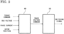
- FIG. 2 shows a function block diagram of the control device 30 of Embodiment 1.
- the control device 30 includes a voltage command generation unit 40 and a switching signal generation unit 50.
- the voltage command generation unit 40 generates phase voltage commands vu*, vv*, and vw* for the respective phases that are calculated on the basis of an externally inputted torque command or current command, a bus voltage Vdc [V], three-phase current values iu [A], iv [A ⁇ , and iw [A] acquired by the current detector 21, and a rotor position ⁇ acquired by the angle detector 22 and that are normalized by Vdc/2.
- the switching signal generation unit 50 generates a switching signal on the basis of comparison between a phase voltage command and a triangular wave that is a carrier.
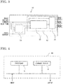
- the switching signal generation unit 50 includes a voltage variation time estimation unit 51 and a switching signal manipulation unit 52
- the switching signal manipulation unit 52 includes a carrier generation unit 53 and a triangular wave comparison PWM unit 54.
- switching signals for turning on the upper arm switch (P side) of each phase and turning off the lower arm switch (N side) of each phase when a voltage command is larger than a triangular wave and turning off the upper arm switch (P side) of each phase and turning on the lower arm switch (N side) of each phase when the voltage command is smaller than the triangular wave are generated.
- an ON signal is generated with a delay of a dead time td.
- switching signals for synchronizing rising and falling of terminal voltages between two phases are generated by performing triangular wave comparison with different carriers for three phases.
- FIG. 4 shows an example of hardware of the control device 30 having such a configuration.
- the control device 30 includes a processor 1 and a storage device 2.
- the storage device includes a volatile storage device such as a random access memory and a nonvolatile auxiliary storage device such as a flash memory.
- a nonvolatile auxiliary storage device such as a flash memory.
- an auxiliary storage device that is a hard disk may be provided instead of the flash memory.
- the processor 1 executes a program inputted from the storage device 2, and implements a part or all of the configurations of the control device 30 described above. In this case, the program is inputted from the auxiliary storage device via the volatile storage device to the processor 1.
- the processor 1 may output data such as a calculation result to the volatile storage device of the storage device 2, or may store the data in the auxiliary storage device via the volatile storage device.
- a logic circuit and an analog circuit may be used together.
- control device 30 Operation of the control device 30 until generation of switching signals for synchronizing rising and falling of terminal voltages between two phases will be described in detail below with reference to a flowchart of FIG. 5 .
- the voltage command generation unit 40 calculates phase voltage commands at a top P1 of a U-phase carrier and updates each phase voltage command at the next top of the U-phase carrier (step S102).
- phase voltage commands normalized by the present Vdc/2 are defined as vu1*, vv1*, and vw1*, respectively
- phase voltage commands with which update is performed at the next top P2 of the U-phase carrier and that are normalized by Vdc/2 in the next carrier cycle are defined as vu2*, vv2*, and vw2*, respectively.
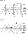
- terminal voltage variation times for U phase as a reference for cancellation are calculated. As shown in FIG. 6 , with the time at the top P2 of the U-phase carrier being set as 0, a rising time tUH [sec] and a falling time tUL [sec] of a U-phase terminal voltage are defined.
- the rising time tUH [sec] and the falling time tUL [sec] of the U-phase terminal voltage are variation times of the U-phase terminal voltage, and are calculated by Expression (1) and Expression (2) on the basis of the U-phase voltage command vu2* generated by the voltage command generation unit 40, and the U-phase carrier cycle Tcu [sec] which is a fixed value (step S103).
- tUH 1 ⁇ vu 2 ⁇ 2 Tcu 2 + Ku ⁇ td
- carrier frequencies at which rising and falling of terminal voltages of V phase and W phase are synchronized with those of U phase are calculated.
- FIG. 6 shows a conceptual diagram showing the calculation method.
- the frequency of the V-phase carrier is updated at tops of the U-phase carrier (P2, P3, etc., in FIG. 6 ).
- a rising frequency of the carrier is defined as Fcv_up [Hz]
- a falling frequency of the carrier is defined as Fcv_dw [Hz].
- a falling time tVL [Hz] of a V-phase terminal voltage is calculated by Expression (3) on the basis of the rising frequency Fcv up [Hz], the V-phase voltage command vv2*, and a time difference ⁇ tuv [sec] between the next top P2 of the U-phase carrier and a bottom Q2 of the V-phase carrier.
- the time differences ⁇ tuv [sec] and ⁇ tuv2 [sec] are parameters for performing adjustment to prevent a time required for rising of the V-phase carrier from exceeding the U-phase carrier cycle Tcu [sec], and need to be set so as to satisfy Expression (6).
- Math. 6 1 2 Fcv _ up _ min + ⁇ tuv ⁇ Tcu + ⁇ tuv 2 ⁇ ⁇ tuv 2 > 1 2 Fcv _ up _ min + ⁇ tuv ⁇ Tcu
- Fcv _ up _ min 1 + vv 2 ⁇ 1 ⁇ vu 2 ⁇ Tcu ⁇ 4 ⁇ tuv ⁇ 4 td
- the falling frequency Fcv_dw [Hz] of the V-phase carrier only needs to be determined such that the time at a bottom Q3 of the V-phase carrier becomes Tcu + ⁇ tuv2 with respect to the next top P3 of the U-phase carrier, and thus the falling frequency Fcv_dw [Hz] can be calculated by Expression (9).
- step S105 a carrier frequency for W phase is calculated.
- a rising frequency Fcw_up [Hz] and a falling frequency Fcw dw [Hz] of a W-phase carrier will be described.
- the carrier frequency for W phase is calculated separately for the case of synchronizing a bottom of the W-phase carrier and a top of the U-phase carrier with each other and for the case of synchronizing a top of the W-phase carrier and a bottom of the U-phase carrier with each other, in accordance with the values of voltage commands for U phase and W phase.
- the carrier frequency for W phase is updated at the tops and the bottoms of the W-phase carrier.
- FIG. 7 shows a conceptual diagram of the method for calculating the carrier frequency for W phase for the case of synchronizing a bottom of the W-phase carrier and a top of the U-phase carrier with each other.
- the rising frequency Fcw_up [Hz] of the W-phase carrier is calculated by Expression (13) such that the carrier cycle of the W-phase carrier is equal to that of the U-phase carrier.
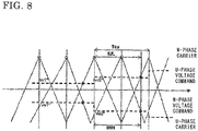
- FIG. 8 shows a conceptual diagram of the W-phase carrier frequency calculating method in this case.
- the next falling frequency Fcw_dw [Hz] of the W-phase carrier and the rising frequency Fcw_up2 [Hz] of the W-phase carrier after the said next falling frequency are calculated.
- the carrier generation unit 53 generates carriers CarrU, CarrV, and CarrW for the respective phases on the basis of: the U-phase carrier frequency Fcu [Hz]; and the rising frequency Fcv up [Hz] and the falling frequency Fcv_dw [Hz] of the V-phase carrier, and the rising frequencies Fcw_up [Hz] and Fcw_up2 [Hz] and the falling frequency Fcw_dw [Hz] of the W phase carrier, all of which are calculated on the basis of Expression (1) to Expression (17) (step S106).
- the U-phase carrier CarrU is generated as a triangular wave that rises and falls at 1/2Fcu.
- the V-phase carrier CarrV is generated as a triangular wave that rises at 1/2Fcv_up and that falls at 1/2Fcv_dw.
- the W-phase carrier is generated as a triangular wave that rises at 1/2Fcw_up or 1/2Fcw_up2 and that falls at 1/2Fcw_dw.
- the triangular wave comparison PWM unit 54 generates switching signals for the upper and lower arms of each phase on the basis of each phase carrier generated by the carrier generation unit 53 and the voltage commands generated by the voltage command generation unit 40 through such calculation (step S107).
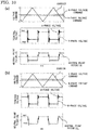
- FIG. 9(a) shows measurement results of terminal voltages and a neutral point potential of U phase and V phase measured with such a configuration
- FIG. 9(b) shows measurement results of terminal voltages and a neutral point potential of U phase and W phase measured with such a configuration
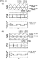
- FIG. 10(a) shows measurement results of terminal voltages and a neutral point potential of U phase and V phase in the case of conventional art in which three-phase carriers are the same
- FIG. 10(b) shows measurement results of terminal voltages and a neutral point potential of U phase and W phase in the case where three-phase carriers are the same.
- FIGS. 11(a) and (b) show measurement results obtained using the method described in Patent Document 2. It is also found that the neutral point potential variation is reduced as compared to the neutral point potential of U phase and V phase (see FIG. 11(a) ) and the neutral point potential of U phase and W phase (see FIG. 11(b) ).
- Embodiment 1 the example in which rising of the terminal voltage of U phase is synchronized with falling of the terminal voltage of V phase and falling of the terminal voltage of U phase is synchronized with rising of the terminal voltage of W phase has been described.
- rising of the terminal voltage of U phase may be synchronized with falling of the terminal voltage of W phase
- falling of the terminal voltage of U phase may be synchronized with rising of the terminal voltage of V phase.
- the phase to be cancelled may be changed to a phase other than U phase.
- the voltage commands are updated at a top of the U-phase carrier every carrier cycle, but the voltage commands may be updated at a bottom of the U-phase carrier, or may be updated every two or more carrier cycles.
- Embodiment 2 an example in which terminal voltage variation is synchronized between phases to reduce neutral point potential variation by manipulating switching signals after triangular wave comparison PWM, will be described.
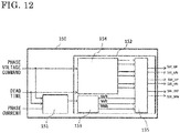
- FIG. 12 shows a function block diagram of a switching signal generation unit 150 in Embodiment 2.
- the configurations of a power converter 10, a rotating machine 20, and a voltage command generation unit 40 in a control device 30 are the same as those of Embodiment 1.
- the hardware configuration is also the same as that shown in FIG. 4 .
- the switching signal generation unit 150 in the control device 30 includes a voltage variation time estimation unit 151 and a switching signal manipulation unit 152, and the switching signal manipulation unit 152 includes a synchronization time calculation unit 153, a triangular wave comparison PWM unit 154, and a synchronization manipulation unit 155.
- rising times and falling times tUH [sec], tUL [sec], tVH [sec], tVL [sec], tWH [sec], and tWL [sec] that are terminal voltage variation times for the respective phases from a top of a U-phase carrier are calculated on the basis of phase voltage commands vu*, vv*, and vw* normalized by Vdc/2, a dead time td [sec], and phase currents iu[A], iv[A], and iw[A].
- Embodiment 2 similar to Embodiment 1, rising and falling of a U-phase terminal voltage are synchronized with either rising or falling of V-phase and W-phase terminal voltages.
- carrier frequencies Fc [Hz] for the three phases are fixed (step S201 in FIG. 13 ).
- the voltage command generation unit 40 calculates each phase voltage command at a top of the U-phase carrier, and updates each phase voltage command at the next top of the U-phase carrier.
- phase voltage commands normalized by the present Vdc/2 are defined as vu1*, vv1*, and vw1*, respectively
- phase voltage commands with which update is performed at the next top of the U-phase carrier and that are normalized by Vdc/2 in the next carrier cycle are defined as vu2*, vv2*, and vw2*, respectively.
- terminal voltage variation times for three phases are calculated at the voltage variation time estimation unit 151 (step S203).
- the rising time tUH [sec] and the falling time tUL [sec] of the U-phase terminal voltage the rising time tVH [sec] and the falling time tVL [sec] of the V-phase terminal voltage, and the rising time tWH [sec] and the falling time tWL [sec] of the W-phase terminal voltage are defined.
- tWH Tc 2 + 1 ⁇ vw 2 ⁇ 2 Tc 2 + Kw ⁇ td
- tWL 1 + vw 2 ⁇ 2 Tc 2 + 1 ⁇ Kw td
- Ku ⁇ 1 iu > 0 0 iu ⁇ 0
- kv ⁇ 1 iv > 0 0 iv ⁇ 0
- Kw ⁇ 1 iw > 0 0 iw ⁇ 0
- switching signals are generated on the basis of triangular wave comparison of the respective phase voltage commands vu*, vv*, and vw* and the respective phase carriers CarrU, CarrV, and CarrW, and switching signals SW_UPtmp, SW_UNtmp, SW_VPtmp, SW_VNtmp, SW_WPtmp, and SW_WNtmp to which a dead time td is added are generated (step S204).
- switching signal manipulation times Usft [sec], Vsft [sec], and Wsft [sec] for the respective phases are calculated on the basis of the differences between the terminal voltage variation times for the respective phases.
- a difference ⁇ UHVL [sec] between the falling time of the V-phase terminal voltage and the rising time of the U-phase terminal voltage, a difference ⁇ UHWL [sec] between the falling time of the W-phase terminal voltage and the rising time of the U-phase terminal voltage, a difference ⁇ ULVH [sec] between the rising time of the V-phase terminal voltage and the falling time of the U-phase terminal voltage, and a difference ⁇ ULWH [sec] between the rising time of the V-phase terminal voltage and the falling time of the U-phase terminal voltage are obtained by Expressions (24) to (27), respectively.
- ⁇ UHVL tUH ⁇ tVL
- UHWL tUH ⁇ tWL
- the switching signal manipulation times Usft, Vsft, and Wsft for synchronizing rising or falling of the U-phase terminal voltage with either rising or falling of the V-phase and W-phase terminal voltages are calculated separately for conditions (A) to (E) based on the magnitude relation between ⁇ UHVL [sec], ⁇ UHWL [sec], ⁇ HLVH [sec], and ⁇ ULWH [sec] (step S205).
- the synchronization manipulation unit 155 respectively generates
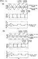
- FIGS. 14(a) and (b) show the terminal voltages and the neutral point potentials of U phase and V phase and of U phase and W phase generated on the basis of the above-described switching signal manipulation.
- each of V phase and W phase may be set as a reference, and the phase that is set as a reference may be changed in accordance with voltage phase.
- each carrier frequency may be variable.
- switching signals capable of synchronizing rising and falling of terminal voltages at least between two phases can be generated under a wide range of driving conditions in which voltage commands are not zero, so that it is possible to reduce neutral point potential variation. Accordingly, it is possible to reduce electromagnetic noise generated with potential variation, so that it is also possible to reduce the size of a noise filter.
- Embodiment 3 Although the example in which triangular wave comparison PWM is applied has been described in Embodiment 1 and Embodiment 2, an example in which ON/OFF of upper and lower arm switches is controlled directly using a time on the basis of voltage command values obtained by a voltage command generation unit will be described in Embodiment 3.
- Embodiment 3 The configurations of a power converter 10, a rotating machine 20, and a voltage command generation unit 40 of a control device 30 of Embodiment 3 are the same as those of Embodiment 1.
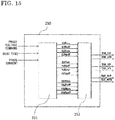
- FIG. 15 shows a function block diagram of a switching signal generation unit 250 in Embodiment 3. Operation of the switching signal generation unit 250 will be sequentially described with reference to a flowchart of FIG. 16 .
- the switching signal generation unit 250 includes a voltage variation time calculation unit 251 and a timer 252.
- the voltage command generation unit 40 generates a voltage command for each phase every control cycle Ts (step S301 in FIG. 16 ).
- phase voltage commands normalized by Vdc/2 in the present control cycle are defined as vu1*, vv1*, and vw1*, respectively
- phase voltage commands normalized by Vdc/2 in the next control cycle are defined as vu2*, vv2*, and vw2*, respectively.
- the average of values detected a plurality of times by the current detector in a control cycle is used, and the detected current is updated every switching cycle (Ts).
- switching times for the upper and lower arms of each phase in the next control cycle are calculated every switching cycle (Ts [sec]) on the basis of the voltage commands vu2*, vv2*, and vw2* with which update is performed in the next cycle, detected currents iu [A], iv [A], and iw [A], and a dead time td [sec].
- the calculation of the switching times is completed immediately before the switching cycle Ts [sec].
- the dead time td is provided to prevent the upper-side switch and the lower-side switch from being turned on at the same time.
- the ON and OFF times for the upper and lower arm switches are calculated separately for cases based on the current polarity of each phase.
- a rising time of the terminal voltage of V phase is tVPon [sec], and a falling time thereof is tVPoff [sec].
- Switching timings are determined such that tUPon [sec] and tVPoff [sec] are equal to each other.
- tVPon td + td + 1 ⁇ vv 2 ⁇ Ts / 2 + td
- a rising time of the terminal voltage of V phase is tVNoff [sec], and a falling time thereof is tVNon [sec].
- Switching timings are determined such that tUPon [sec] and tVNon [sec] are equal to each other.
- tVPon td + 1 ⁇ vv 2 ⁇ Ts / 2 + td
- a rising time of the terminal voltage of W phase is tWPon [sec], and a falling time thereof is tWPoff [sec].
- a rising time of the terminal voltage of W phase is tWNoff [sec], and a falling time thereof is tWNon [sec].
- tWNoff td + 1 + vu 2 ⁇ Ts / 2
- tWPon td + 1 + vu 2 ⁇ Ts / 2 + td
- tWPoff td + 1 + vu 2 ⁇ Ts / 2 + 1 ⁇ vw 2 ⁇ Ts / 2
- tWNon td + 1 + vu 2 ⁇ Ts / 2 + 1 ⁇ vw 2 ⁇ Ts / 2 + td
- tUNon td + 1 + vu 2 ⁇ Ts / 2 + td
- a rising time of the terminal voltage of V phase is tVPon [sec], and a falling time thereof is tVPoff [sec].
- Switching timings are determined such that tUNoff [sec] and tVPoff [sec] are equal to each other.
- tVPon td + 1 ⁇ vv 2 ⁇ Ts / 2 + td
- a rising time of the terminal voltage of V phase is tVNoff [sec], and a falling time thereof is tVNon [sec].
- Switching timings are determined such that tUNoff [sec] and tVNon [sec] are equal to each other.
- tVNoff 1 ⁇ vv 2 ⁇ Ts / 2
- tVPon 1 ⁇ vv 2 ⁇ Ts / 2 + td
- a rising time of the terminal voltage of W phase is tWPon [sec], and a falling time thereof is tWPoff [sec].
- Switching timings are determined such that tUNon [sec] and tWPon [sec] are equal to each other.
- tWNoff td + 1 + vu 2 ⁇ Ts / 2
- tWPon td + 1 + vu 2 ⁇ Ts / 2 + td
- tWPoff td + 1 + vu 2 ⁇ Ts / 2 + 1 ⁇ vw 2 ⁇ Ts / 2
- tWNon td + 1 + vu 2 ⁇ Ts / 2 + 1 ⁇ vw 2 ⁇ Ts / 2 + td
- a rising time of the terminal voltage of W phase is tWNoff [sec], and a falling time thereof is tWNon [sec].
- the timer 252 generates switching signals for the upper and lower arms of each phase on the basis of the switching times for the upper and lower arms of each phase that are calculated by the voltage variation time calculation unit 251.
- the timer 252 adjusts the ON and OFF times for the upper and lower arm switches of each phase and generates switching signals (step S304). ON/OFF of the switches of each phase is controlled on the basis of the switching signals generated by the timer 252.
- the upper arm switch of V phase (preferably, a phase having a positive phase current) is turned off, and the lower arm switch of V phase is turned on after the dead time td [sec] with the time of detection of rising of the terminal voltage of U phase as a reference (0 [sec]).
- the lower arm switch of V phase is turned off after (1 - vv1*)Ts/2, and the upper arm switch of V phase is turned on after ((1 - vv1*)Ts/2 + td).
- the lower arm switch of W phase (preferably, a phase having a negative phase current) is turned off, and the upper arm switch of W phase is turned on after the dead time td [sec] with the time of detection of falling of the terminal voltage of U phase as a reference (0 [sec]).
- the upper arm switch of W phase is turned off after (1 + vw1*)Ts/2, and the upper arm switch of V phase is turned on after ((1 + vw1*)Ts/2 + td).
- control device which generates switching signals for the upper and lower arms of each phase is configured to include the voltage variation time calculation unit 251 and the timer 252, switching signals capable of synchronizing rising and falling of terminal voltages at least between two phases can be generated under a wide range of driving conditions in which voltage commands are not zero, regardless of a modulation factor, with a simple configuration not using triangular wave comparison PWM. Accordingly, it is possible to reduce neutral point potential variation, and electromagnetic noise generated with potential variation can be reduced. In addition, it is also possible to reduce the size of a noise filter.
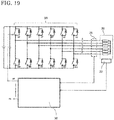
- Embodiments 1 to 3 the example of the configuration of the three-phase inverter as the power converter 10 has been described. However, by using a configuration such as a six-phase inverter as the power converter 10 as shown in FIG. 19 and controlling the control device 30 in the same manner as described in Embodiments 1 to 3, rising and falling of terminal voltages between two phases may be synchronized based on A phase.
- the effect of reducing neutral point potential variation is obtained as shown in FIG. 21(b) , as compared to a conventional method shown in FIG. 21(a) , by setting the phase difference between carriers for two phases (for example, A phase and D phase in FIG. 20 ) for which the phases of the phase voltage commands are different from each other by 180° to 180°.
- Embodiments 1 to 3 the example in which the one three-phase rotating machine 20 is driven by the three-phase inverter as the power converter 10 has been described.
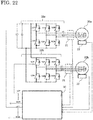
- a drive system that drives three-phase rotating machines 20a and 20b with two three-phase inverters 10a and 10b as shown in FIG. 22 may perform control in which not only rising and falling of terminal voltages between two phases in the same inverter 10a but also rising and falling of terminal voltages between two phases in the inverter 10a and the inverter 10b are synchronized by controlling the control device 30 in the same manner as described in Embodiments 1 to 3.
- the effect of reducing neutral point potential variation is obtained, similar to that shown in FIG. 21(b) , by setting the phase difference between carriers for two phases (for example, U1 phase and U2 phase in FIG. 23 ) for which the phases of the phase voltage commands are different from each other by 180° to 180°.
Landscapes
- Engineering & Computer Science (AREA)
- Power Engineering (AREA)
- Physics & Mathematics (AREA)
- Electromagnetism (AREA)
- Inverter Devices (AREA)
Abstract
Description
- The present disclosure relates to a power conversion device and a rotating machine drive system.
- In a converter that controls an output voltage by ON/OFF of switching elements, when each phase terminal voltage varies in switching operation, leakage current is generated via a stray capacitance with respect to the ground, and electromagnetic noise is generated.
- Since electromagnetic noise standards are defined for each product category, measures need to be taken if the electromagnetic noise generated in a power converter exceeds regulations. In general, measures against electromagnetic noise are taken by a noise filter composed of a passive element. However, there are problems of securing a space occupied by the power converter and cost due to the filter.
- Therefore, a technology to reduce electromagnetic noise by adjusting the phase of a carrier that determines ON/OFF of switching elements has been proposed in a conventional control device for a power converter (see, for example,
Patent Document 1 and Patent Document 2). -
- Patent Document 1: Japanese Laid-Open Patent Publication
JP 2008-271 617 A lines 18 to 29,FIG. 5 ,FIG. 6 ) - Patent Document 2: Japanese Laid-Open Patent Publication
JP 2016-208 664 A page 6,lines 6 to 24,FIG. 3 ) - In a method described in
Patent Document 1, by providing a phase difference in the carrier for each phase, the maximum value and the minimum value of the neutral point potential can be reduced, but the frequency of variation of the neutral point potential does not decrease. Thus, there is a problem that the effect of reducing electromagnetic noise is small. - Meanwhile, in a method described in
Patent Document 2, by canceling terminal voltage variation between phases, the frequency of variation of the neutral point potential can be reduced, and thus the effect of reducing electromagnetic noise increases. However, the proposed method is effective only when a voltage command is substantially zero, and there is a problem that the effect of reducing electromagnetic noise decreases as a modulation factor increases. - The present disclosure has been made to solve the above-described problems, and an object of the present disclosure is to obtain a power conversion device capable of reducing electromagnetic noise under a wide range of driving conditions.
- A power conversion device according to the present disclosure is a power conversion device including: a power converter in which a plurality of one-phase legs each including an upper arm switching element and a lower arm switching element are connected in parallel to a DC power supply and connection points between the upper arm switching elements and the lower arm switching elements are connected to a load; and a control device for controlling switching operation of the upper arm switching elements and the lower arm switching elements of the power converter, the power conversion device converting DC power to AC power and supplying the AC power to the load, wherein the control device performs switching control such that, on the basis of a rising time and a falling time of a terminal voltage of a connection point, connected to the load, of a first one-phase leg, at least the rising time of the terminal voltage of the first one-phase leg and a falling time of a terminal voltage of a second one-phase leg or the falling time of the terminal voltage of the first one-phase leg and a rising time of the terminal voltage of the second one-phase leg are synchronized with each other.
- With the power conversion device according to the present disclosure, it is possible to synchronize terminal voltages at least between two phases under a wide range of driving conditions, and it is possible to reduce electromagnetic noise generated with neutral point potential variation.
-
- FIG. 1
- shows the configuration of a control device for a power converter according to
Embodiment 1. - FIG. 2
- is a function block diagram of the control device of
Embodiment 1. - FIG. 3
- is a function block diagram of a switching signal generation unit of
Embodiment 1. - FIG. 4
- shows an example of hardware of the control device of
Embodiment 1. - FIG. 5
- is a flowchart showing operation of the switching signal generation unit of
Embodiment 1. - FIG. 6
- is a conceptual diagram showing a method for calculating a V-phase carrier frequency according to
Embodiment 1. - FIG. 7
- is a conceptual diagram showing a method for calculating a W-phase carrier frequency according to
Embodiment 1. - FIG. 8
- is another conceptual diagram showing the method for calculating a W-phase carrier frequency according to
Embodiment 1. - FIG. 9(a)
- shows terminal voltages and a neutral point potential of U phase and V phase according to
Embodiment 1. - FIG. 9(b)
- shows terminal voltages and a neutral point potential of U phase and W phase according to
Embodiment 1. - FIG. 10(a)
- shows terminal voltages and a neutral point potential of U phase and V phase by conventional triangular wave comparison PWM.
- FIG. 10(b)
- shows terminal voltages and a neutral point potential of U phase and W phase by the conventional triangular wave comparison PWM.
- FIG. 11(a)
- shows terminal voltages and a neutral point potential of U phase and V phase by a conventional method before switching signal manipulation.
- FIG. 11(b)
- shows terminal voltages and a neutral point potential of U phase and W phase by the conventional method before switching signal manipulation.
- FIG. 12
- is a function block diagram of a switching signal generation unit of
Embodiment 2. - FIG. 13
- is a flowchart showing operation of the switching signal generation unit of
Embodiment 2. - FIG. 14(a)
- shows terminal voltages and a neutral point potential of U phase and V phase after switching signal manipulation in
Embodiment 2. - FIG. 14(b)
- shows terminal voltages and a neutral point potential of U phase and W phase after switching signal manipulation in
Embodiment 2. - FIG. 15
- is a function block diagram of a switching signal generation unit of Embodiment 3.
- FIG. 16
- is a flowchart showing operation of the switching signal generation unit of Embodiment 3.
- FIG. 17
- shows an example of each phase terminal voltage in Embodiment 3.
- FIG. 18
- is a diagram for explaining delays of ON times and OFF times of terminal voltages according to Embodiment 3.
- FIG. 19
- shows the configuration of a six-phase inverter to which
Embodiments 1 to 3 are applied. - FIG. 20
- is a diagram for explaining phase voltage commands for six phases to which
Embodiments 1 to 3 are applied. - FIG. 21(a)
- shows conventional terminal voltages and neutral point potential for comparison with Embodiment 3.
FIG. 21(b) shows an example of terminal voltages and neutral point potential to which Embodiment 3 is applied. - FIG. 22
- shows a configuration to which
Embodiments 1 to 3 are applied and in which two rotating machines are driven by two three-phase inverters. - FIG. 23
- is a diagram for explaining each of phase voltage commands of the two three-phase inverters to which
Embodiments 1 to 3 are applied. -
FIG. 1 shows a control device for a power converter according toEmbodiment 1.Embodiment 1 will be described with an example in which the control device is applied to a three-phase rotating machine drive system with a three-phase inverter. - In
FIG. 1 , the three-phase rotating machine drive system includes apower converter 10 that converts DC power to three-phase AC power, a rotatingmachine 20 that is supplied with power and driven by thepower converter 10, and acontrol device 30 that controls thepower converter 10. - A DC bus of the
power converter 10 is connected to aDC power supply 11. Thepower converter 10 includes a smoothingcapacitor 12 on the DC bus. Thepower converter 10 has switchingelements 13 including a U-phaseupper arm switch 13a, a U-phaselower arm switch 13b, a V-phaseupper arm switch 13c, a V-phaselower arm switch 13d, a W-phaseupper arm switch 13e, and a W-phaselower arm switch 13f. The upper and lower arm switches of each phase are connected in series. The upper and lower arm switches of the respective phases, which are connected in series, are connected in parallel to the DC bus and form a three-phase inverter. Each switchingelement 13 is composed of, for example, a MOSFET (metal-oxide-semiconductor field-effect transistor) or the like. - A U-phase output terminal of the rotating
machine 20 is connected to the arm connection point between the U-phaseupper arm switch 13a and the U-phaselower arm switch 13b, a V-phase output terminal of the rotatingmachine 20 is connected to the arm connection point between the V-phaseupper arm switch 13c and the V-phaselower arm switch 13d, and a W-phase output terminal of the rotatingmachine 20 is connected to the arm connection point between the W-phaseupper arm switch 13e and the W-phaselower arm switch 13f. - The potential of the connection point, between the upper and lower arms of each phase, to which each phase terminal of the rotating
machine 20 is connected is defined as a terminal voltage of each phase. - The rotating
machine 20 includes acurrent detector 21 that detects a current of each phase, and anangle detector 22 that detects a rotor angle. - ON/OFF of the arm switches 13a to 13f of the respective phases is controlled on the basis of switching signals SW_UP, SW_UN, SW_VP, SW_VN, SW_WP, and SW_WN generated by the
control device 30. -
FIG. 2 shows a function block diagram of thecontrol device 30 ofEmbodiment 1. Thecontrol device 30 includes a voltagecommand generation unit 40 and a switchingsignal generation unit 50. The voltagecommand generation unit 40 generates phase voltage commands vu*, vv*, and vw* for the respective phases that are calculated on the basis of an externally inputted torque command or current command, a bus voltage Vdc [V], three-phase current values iu [A], iv [A}, and iw [A] acquired by thecurrent detector 21, and a rotor position θ acquired by theangle detector 22 and that are normalized by Vdc/2. - The switching
signal generation unit 50 generates a switching signal on the basis of comparison between a phase voltage command and a triangular wave that is a carrier. Specifically, as shown inFIG. 3 , the switchingsignal generation unit 50 includes a voltage variationtime estimation unit 51 and a switchingsignal manipulation unit 52, and the switchingsignal manipulation unit 52 includes acarrier generation unit 53 and a triangular wavecomparison PWM unit 54. - In generation of switching signals by the triangular wave
comparison PWM unit 54, switching signals for turning on the upper arm switch (P side) of each phase and turning off the lower arm switch (N side) of each phase when a voltage command is larger than a triangular wave and turning off the upper arm switch (P side) of each phase and turning on the lower arm switch (N side) of each phase when the voltage command is smaller than the triangular wave, are generated. - At this time, to prevent the upper and lower arm switches from being turned on at the same time, when the P-side and N-side switches are turned on, an ON signal is generated with a delay of a dead time td. At the triangular wave
comparison PWM unit 54, switching signals for synchronizing rising and falling of terminal voltages between two phases are generated by performing triangular wave comparison with different carriers for three phases. -
FIG. 4 shows an example of hardware of thecontrol device 30 having such a configuration. Thecontrol device 30 includes aprocessor 1 and astorage device 2. Although not shown, the storage device includes a volatile storage device such as a random access memory and a nonvolatile auxiliary storage device such as a flash memory. Alternatively, an auxiliary storage device that is a hard disk may be provided instead of the flash memory. Theprocessor 1 executes a program inputted from thestorage device 2, and implements a part or all of the configurations of thecontrol device 30 described above. In this case, the program is inputted from the auxiliary storage device via the volatile storage device to theprocessor 1. - In addition, the
processor 1 may output data such as a calculation result to the volatile storage device of thestorage device 2, or may store the data in the auxiliary storage device via the volatile storage device. Moreover, in addition to theprocessor 1 and thestorage device 2, a logic circuit and an analog circuit may be used together. - Operation of the
control device 30 until generation of switching signals for synchronizing rising and falling of terminal voltages between two phases will be described in detail below with reference to a flowchart ofFIG. 5 . - As a premise, a carrier frequency Fcu [Hz] for U phase is fixed (step S101 in
FIG. 5 ). Therefore, a U-phase carrier cycle Tcu [sec] is defined as Tcu = 1/Fcu. - For example, in
FIG. 6 , the voltagecommand generation unit 40 calculates phase voltage commands at a top P1 of a U-phase carrier and updates each phase voltage command at the next top of the U-phase carrier (step S102). Here, phase voltage commands normalized by the present Vdc/2 are defined as vu1*, vv1*, and vw1*, respectively, and phase voltage commands with which update is performed at the next top P2 of the U-phase carrier and that are normalized by Vdc/2 in the next carrier cycle are defined as vu2*, vv2*, and vw2*, respectively. After calculation of each phase voltage command is completed, calculation of each phase carrier frequency is started. - At the voltage variation
time estimation unit 51, terminal voltage variation times for U phase as a reference for cancellation are calculated. As shown inFIG. 6 , with the time at the top P2 of the U-phase carrier being set as 0, a rising time tUH [sec] and a falling time tUL [sec] of a U-phase terminal voltage are defined. - The rising time tUH [sec] and the falling time tUL [sec] of the U-phase terminal voltage are variation times of the U-phase terminal voltage, and are calculated by Expression (1) and Expression (2) on the basis of the U-phase voltage command vu2* generated by the voltage
command generation unit 40, and the U-phase carrier cycle Tcu [sec] which is a fixed value (step S103).
[Math. 1]

- Next, at the
carrier generation unit 53, carrier frequencies at which rising and falling of terminal voltages of V phase and W phase are synchronized with those of U phase are calculated. - First, a frequency of a V-phase carrier is calculated (step S104).
FIG. 6 shows a conceptual diagram showing the calculation method. - The frequency of the V-phase carrier is updated at tops of the U-phase carrier (P2, P3, etc., in
FIG. 6 ). A rising frequency of the carrier is defined as Fcv_up [Hz], and a falling frequency of the carrier is defined as Fcv_dw [Hz]. - A falling time tVL [Hz] of a V-phase terminal voltage is calculated by Expression (3) on the basis of the rising frequency Fcv up [Hz], the V-phase voltage command vv2*, and a time difference Δtuv [sec] between the next top P2 of the U-phase carrier and a bottom Q2 of the V-phase carrier.
[Math. 3]
- If the rising time tUH [sec] of the U-phase terminal voltage and the falling time tVL [sec] of the V-phase terminal voltage are equal to each other, it is possible to synchronize rising and falling of the terminal voltages, and thus Expression (4) only needs to be satisfied.
[Math. 4]
- The rising frequency Fcv up [Hz] of the V-phase carrier that satisfies Expression (4) on the basis of Expressions (1) and (3) is obtained by Expression (5).
[Math. 5]

- Here, the method for calculating the time difference Δtuv [sec] will be described.
- The time differences Δtuv [sec] and Δtuv2 [sec] are parameters for performing adjustment to prevent a time required for rising of the V-phase carrier from exceeding the U-phase carrier cycle Tcu [sec], and need to be set so as to satisfy Expression (6).
[Math. 6]
- Here, Fcv_up_min [Hz] is the minimum value of the rising frequency of the V-phase carrier, corresponds to Fcv up [Hz] when Kuv = -1 in Expression (5), and is calculated by Expression (7).
[Math. 7]
- The time difference Δtuv2 [sec] that prevents the time required for rising of the V-phase carrier from exceeding the U-phase carrier cycle Tcu on the basis of Expression (6) and Expression (7) can be calculated by Expression (8).
[Math. 8]
- Moreover, the falling frequency Fcv_dw [Hz] of the V-phase carrier only needs to be determined such that the time at a bottom Q3 of the V-phase carrier becomes Tcu + Δtuv2 with respect to the next top P3 of the U-phase carrier, and thus the falling frequency Fcv_dw [Hz] can be calculated by Expression (9).
[Math. 9]
- Next, a carrier frequency for W phase is calculated (step S105).
- A rising frequency Fcw_up [Hz] and a falling frequency Fcw dw [Hz] of a W-phase carrier will be described.
- The carrier frequency for W phase is calculated separately for the case of synchronizing a bottom of the W-phase carrier and a top of the U-phase carrier with each other and for the case of synchronizing a top of the W-phase carrier and a bottom of the U-phase carrier with each other, in accordance with the values of voltage commands for U phase and W phase. The carrier frequency for W phase is updated at the tops and the bottoms of the W-phase carrier.
- First, calculation for the case of synchronizing a bottom of the W-phase carrier and a top of the U-phase carrier with each other is started.
FIG. 7 shows a conceptual diagram of the method for calculating the carrier frequency for W phase for the case of synchronizing a bottom of the W-phase carrier and a top of the U-phase carrier with each other. - At this time, a rising time tWH [sec] of a W-phase terminal voltage can be calculated by Expression (10).
[Math. 10]
- If the falling time tUL [sec] of the U-phase terminal voltage and the rising time tWH [sec] of the W-phase terminal voltage become equal to each other, it is possible to synchronize rising and falling of the terminal voltages, and thus Expression (11) only needs to be satisfied.
[Math. 11]
- The falling frequency Fcw dw [Hz] of the W-phase carrier that satisfies Expression (11) on the basis of Expression (2) and Expression (10) can be obtained by Expression (12).
[Math. 12]

- The rising frequency Fcw_up [Hz] of the W-phase carrier is calculated by Expression (13) such that the carrier cycle of the W-phase carrier is equal to that of the U-phase carrier.
[Math. 13]
- Next, a condition for synchronizing a top of the W-phase carrier with a bottom of the U-phase carrier will be described.
FIG. 8 shows a conceptual diagram of the W-phase carrier frequency calculating method in this case. - When Fcw_dw < Fcu/2 in Expression (12), a bottom of the W-phase carrier cannot be synchronized with a top of the U-phase carrier, and thus a transition is made to the case of synchronizing a top of the W-phase carrier and a bottom of the U-phase carrier with each other. In the transition, the rising frequency Fcw up [Hz] of the W-phase carrier is provided by Expression (14), and a top of the W-phase carrier is synchronized with a bottom of the U-phase carrier.
[Math. 14]
- The next falling frequency Fcw_dw [Hz] of the W-phase carrier and the rising frequency Fcw_up2 [Hz] of the W-phase carrier after the said next falling frequency are calculated.
- Under the condition for synchronizing a top of the W-phase carrier with a bottom of the U-phase carrier, the rising time tWH [sec] of the W-phase terminal voltage can be calculated by Expression (15).
[Math. 15]
- The falling frequency Fcw dw [Hz] of the W-phase carrier that satisfies Expression (11) on the basis of Expression (2) and Expression (15) can be calculated by Expression (16).
[Math. 16]
- In addition, the rising frequency Fcw_up2 [Hz] of the W-phase carrier after the said next falling frequency is calculated by Expression (17) such that the cycle of the W-phase carrier is equal to that of the U-phase carrier.
[Math. 17]
- When Fcw_dw < Fcu in Expression (16), a transition is made to the condition for synchronizing a bottom of the W-phase carrier and a top of the U-phase carrier with each other.
- The
carrier generation unit 53 generates carriers CarrU, CarrV, and CarrW for the respective phases on the basis of: the U-phase carrier frequency Fcu [Hz]; and the rising frequency Fcv up [Hz] and the falling frequency Fcv_dw [Hz] of the V-phase carrier, and the rising frequencies Fcw_up [Hz] and Fcw_up2 [Hz] and the falling frequency Fcw_dw [Hz] of the W phase carrier, all of which are calculated on the basis of Expression (1) to Expression (17) (step S106). - Specifically, the U-phase carrier CarrU is generated as a triangular wave that rises and falls at 1/2Fcu. The V-phase carrier CarrV is generated as a triangular wave that rises at 1/2Fcv_up and that falls at 1/2Fcv_dw. The W-phase carrier is generated as a triangular wave that rises at 1/2Fcw_up or 1/2Fcw_up2 and that falls at 1/2Fcw_dw.
- The triangular wave
comparison PWM unit 54 generates switching signals for the upper and lower arms of each phase on the basis of each phase carrier generated by thecarrier generation unit 53 and the voltage commands generated by the voltagecommand generation unit 40 through such calculation (step S107). -
FIG. 9(a) shows measurement results of terminal voltages and a neutral point potential of U phase and V phase measured with such a configuration, andFIG. 9(b) shows measurement results of terminal voltages and a neutral point potential of U phase and W phase measured with such a configuration. For comparison,FIG. 10(a) shows measurement results of terminal voltages and a neutral point potential of U phase and V phase in the case of conventional art in which three-phase carriers are the same, andFIG. 10(b) shows measurement results of terminal voltages and a neutral point potential of U phase and W phase in the case where three-phase carriers are the same. It is found that, as compared to conventional switching by triangular wave comparison PWM in the case where three-phase carriers are the same, in switching according to the present embodiment, the falling times and the rising times of terminal voltages between two phases are synchronized, and the neutral point potential is reduced. - Furthermore,
FIGS. 11(a) and (b) show measurement results obtained using the method described inPatent Document 2. It is also found that the neutral point potential variation is reduced as compared to the neutral point potential of U phase and V phase (seeFIG. 11(a) ) and the neutral point potential of U phase and W phase (seeFIG. 11(b) ). - As presented above, in
Embodiment 1, the example in which rising of the terminal voltage of U phase is synchronized with falling of the terminal voltage of V phase and falling of the terminal voltage of U phase is synchronized with rising of the terminal voltage of W phase has been described. However, rising of the terminal voltage of U phase may be synchronized with falling of the terminal voltage of W phase, and falling of the terminal voltage of U phase may be synchronized with rising of the terminal voltage of V phase. Alternatively, the phase to be cancelled may be changed to a phase other than U phase. - Moreover, the example in which the carrier frequency is manipulated has been described, but the same effects are also achieved by manipulating each phase voltage command value.
- Furthermore, in
Embodiment 1, the example in which the voltage commands are updated at a top of the U-phase carrier every carrier cycle has been described, but the voltage commands may be updated at a bottom of the U-phase carrier, or may be updated every two or more carrier cycles. - With such a configuration, in the control device which generates switching signals for the upper and lower arms of each phase by triangular wave comparison PWM, regardless of a modulation factor, carriers capable of synchronizing rising and falling of terminal voltages at least between two phases can be generated under a wide range of driving conditions in which voltage commands are not zero, so that it is possible to reduce neutral point potential variation. Accordingly, it is possible to reduce electromagnetic noise generated with potential variation. Furthermore, since it is possible to reduce electromagnetic noise, it is also possible to reduce the size of a noise filter.
- In
Embodiment 2, an example in which terminal voltage variation is synchronized between phases to reduce neutral point potential variation by manipulating switching signals after triangular wave comparison PWM, will be described. - As a method for synchronizing terminal voltage variation of each phase having different polarities by manipulating switching signals after triangular wave comparison PWM, the following two methods are assumed:
- (1) a method of manipulating switching signals in the next cycle on the basis of voltage commands in the next cycle; and
- (2) a method of detecting rising and falling of present switching signals generated and time-shifting the signals until a switching signal time to be synchronized is detected.
-
FIG. 12 shows a function block diagram of a switchingsignal generation unit 150 inEmbodiment 2. - The configurations of a
power converter 10, a rotatingmachine 20, and a voltagecommand generation unit 40 in acontrol device 30 are the same as those ofEmbodiment 1. The hardware configuration is also the same as that shown inFIG. 4 . - The switching
signal generation unit 150 in thecontrol device 30 includes a voltage variationtime estimation unit 151 and a switchingsignal manipulation unit 152, and the switchingsignal manipulation unit 152 includes a synchronizationtime calculation unit 153, a triangular wavecomparison PWM unit 154, and asynchronization manipulation unit 155. - Next, operation of the switching
signal generation unit 150 ofEmbodiment 2 will be sequentially described with reference to a flowchart ofFIG. 13 . - First, at the voltage variation
time estimation unit 151, rising times and falling times tUH [sec], tUL [sec], tVH [sec], tVL [sec], tWH [sec], and tWL [sec] that are terminal voltage variation times for the respective phases from a top of a U-phase carrier are calculated on the basis of phase voltage commands vu*, vv*, and vw* normalized by Vdc/2, a dead time td [sec], and phase currents iu[A], iv[A], and iw[A]. - In
Embodiment 2, similar toEmbodiment 1, rising and falling of a U-phase terminal voltage are synchronized with either rising or falling of V-phase and W-phase terminal voltages. In addition, carrier frequencies Fc [Hz] for the three phases are fixed (step S201 inFIG. 13 ). Each carrier cycle is defined as Tc (= 1/Fc). - Similar to
Embodiment 1, an example in which the V-phase and W-phase carriers are inverted with respect to the U-phase carrier will be described. The voltagecommand generation unit 40 calculates each phase voltage command at a top of the U-phase carrier, and updates each phase voltage command at the next top of the U-phase carrier. Here, phase voltage commands normalized by the present Vdc/2 are defined as vu1*, vv1*, and vw1*, respectively, and phase voltage commands with which update is performed at the next top of the U-phase carrier and that are normalized by Vdc/2 in the next carrier cycle are defined as vu2*, vv2*, and vw2*, respectively. - After calculation of the respective phase voltage commands vu2*, vv2*, and vw2* (step S202), terminal voltage variation times for three phases are calculated at the voltage variation time estimation unit 151 (step S203).
- With the time at the next top of the U-phase carrier being set as
time 0, the rising time tUH [sec] and the falling time tUL [sec] of the U-phase terminal voltage, the rising time tVH [sec] and the falling time tVL [sec] of the V-phase terminal voltage, and the rising time tWH [sec] and the falling time tWL [sec] of the W-phase terminal voltage are defined. - The terminal voltage variation times for the respective phases can be estimated by Expressions (18) to (23).
[Math. 18]


- Next, operation of the switching
signal manipulation unit 152 will be described. In the switchingsignal manipulation unit 152, at the triangular wavecomparison PWM unit 154, switching signals are generated on the basis of triangular wave comparison of the respective phase voltage commands vu*, vv*, and vw* and the respective phase carriers CarrU, CarrV, and CarrW, and switching signals SW_UPtmp, SW_UNtmp, SW_VPtmp, SW_VNtmp, SW_WPtmp, and SW_WNtmp to which a dead time td is added are generated (step S204). - At the synchronization
time calculation unit 153, switching signal manipulation times Usft [sec], Vsft [sec], and Wsft [sec] for the respective phases are calculated on the basis of the differences between the terminal voltage variation times for the respective phases. - First, a difference ΔUHVL [sec] between the falling time of the V-phase terminal voltage and the rising time of the U-phase terminal voltage, a difference ΔUHWL [sec] between the falling time of the W-phase terminal voltage and the rising time of the U-phase terminal voltage, a difference ΔULVH [sec] between the rising time of the V-phase terminal voltage and the falling time of the U-phase terminal voltage, and a difference ΔULWH [sec] between the rising time of the V-phase terminal voltage and the falling time of the U-phase terminal voltage are obtained by Expressions (24) to (27), respectively.


- Next, the switching signal manipulation times Usft, Vsft, and Wsft for synchronizing rising or falling of the U-phase terminal voltage with either rising or falling of the V-phase and W-phase terminal voltages are calculated separately for conditions (A) to (E) based on the magnitude relation between ΔUHVL [sec], ΔUHWL [sec], ΔHLVH [sec], and ΔULWH [sec] (step S205).
- (A) When ΔUHVL < 0, ΔUHWL < 0, ΔULVH > 0, and ΔULWH > 0,
- (a) when ΔUHVL < ΔUHWL,
- Usft = |ΔUHVL|
- Vsft = 0
- Wsft = ΔULWH + |ΔUHVL|
- (b) when ΔUHVL ≥ ΔUHWL,
- Usft = |ΔUHWL|
- Vsft = ΔULVH + |ΔUHWL|
- Wsft = 0.
- (a) when ΔUHVL < ΔUHWL,
- (B) When ΔUHVL > 0, ΔUHWL > 0, ΔULVH < 0, and ΔULWH < 0,
- (a) when ΔULVH < ΔULWH,
- Usft = |ΔULVH|
- Vsft = 0
- Wsft = ΔUHWL + |ΔULVH|
- (b) when ΔULVH ≥ΔULWH,
- Usft = |ΔULWH|
- Vsft = ΔUHVL + |ΔULWH|
- Wsft = 0.
- (a) when ΔULVH < ΔULWH,
- (C) When ΔUHVL < 0, ΔUHWL > 0, ΔULVH > 0, and ΔULWH < 0,
- Usft = 0
- Vsft = ΔULVH
- Wsft = ΔUHWL.
- (D) When ΔUHVL > 0, ΔUHWL < 0, ΔULVH < 0, and ΔULWH > 0,
- Usft = 0
- Vsft = ΔUHVL
- Wsft = ΔULWH.
- (E) At times other than the above,
- Usft = 0
- Vsft = 0
- Wsft = 0.
- Finally, on the basis of the switching signals SW_UPtmp, SW_UNtmp, SW_VPtmp, SW_VNtmp, SW_WPtmp, and SW_WNtmp for the respective phases outputted by the triangular wave
comparison PWM unit 154, thesynchronization manipulation unit 155 respectively generates - (1) switching signals SW_UP and SW_UN obtained by time-shifting the U-phase switching signals SW_UPtmp and SW_UNtmp by the manipulation time Usft [sec],
- (2) switching signals SW_VP and SW_VN obtained by time-shifting the V-phase switching signals SW_VPtmp and SW_VNtmp by the manipulation time Vsft [sec], and
- (3) switching signals SW_WP and SW_WN obtained by time-shifting the W-phase switching signals SW_WPtmp and SW_WNtmp by the manipulation time Wsft [sec] (step S206).
-
FIGS. 14(a) and (b) show the terminal voltages and the neutral point potentials of U phase and V phase and of U phase and W phase generated on the basis of the above-described switching signal manipulation. - It is confirmed that, as compared to
FIGS. 11(a) and (b) showing the three-phase terminal voltages and the neutral point potentials in the case where switching signals are not manipulated, neutral point potential variation is reduced by synchronizing the U-phase terminal voltage variation with the V-phase and W-phase terminal voltage variation. - In
Embodiment 2, the example in which the U-phase terminal voltage variation is synchronized with the V-phase and W-phase terminal voltage variation has been described, but each of V phase and W phase may be set as a reference, and the phase that is set as a reference may be changed in accordance with voltage phase. In addition, each carrier frequency may be variable. - With such a configuration, in the control device which generates switching signals for the upper and lower arms of each phase by triangular wave comparison PWM, regardless of a modulation factor, switching signals capable of synchronizing rising and falling of terminal voltages at least between two phases can be generated under a wide range of driving conditions in which voltage commands are not zero, so that it is possible to reduce neutral point potential variation. Accordingly, it is possible to reduce electromagnetic noise generated with potential variation, so that it is also possible to reduce the size of a noise filter.
- Although the example in which triangular wave comparison PWM is applied has been described in
Embodiment 1 andEmbodiment 2, an example in which ON/OFF of upper and lower arm switches is controlled directly using a time on the basis of voltage command values obtained by a voltage command generation unit will be described in Embodiment 3. - The configurations of a
power converter 10, a rotatingmachine 20, and a voltagecommand generation unit 40 of acontrol device 30 of Embodiment 3 are the same as those ofEmbodiment 1. -
FIG. 15 shows a function block diagram of a switchingsignal generation unit 250 in Embodiment 3. Operation of the switchingsignal generation unit 250 will be sequentially described with reference to a flowchart ofFIG. 16 . - The switching
signal generation unit 250 includes a voltage variationtime calculation unit 251 and atimer 252. The voltagecommand generation unit 40 generates a voltage command for each phase every control cycle Ts (step S301 inFIG. 16 ). - At a predetermined time (for example, time T1 in
FIG. 17 ), calculation of each phase voltage command is started, and the calculated voltage commands are reflected in the next control cycle. Here, phase voltage commands normalized by Vdc/2 in the present control cycle are defined as vu1*, vv1*, and vw1*, respectively, and phase voltage commands normalized by Vdc/2 in the next control cycle are defined as vu2*, vv2*, and vw2*, respectively. - As a detected current, the average of values detected a plurality of times by the current detector in a control cycle is used, and the detected current is updated every switching cycle (Ts).
- At the voltage variation
time calculation unit 251, switching times for the upper and lower arms of each phase in the next control cycle are calculated every switching cycle (Ts [sec]) on the basis of the voltage commands vu2*, vv2*, and vw2* with which update is performed in the next cycle, detected currents iu [A], iv [A], and iw [A], and a dead time td [sec]. The calculation of the switching times is completed immediately before the switching cycle Ts [sec]. - In accordance with each phase voltage command and the polarity of each detected current, ON and OFF times for the upper and lower arm switches are calculated on the basis of the next cycle time T2 = 0 in the following manner. Each switching time is manipulated between 0 and 2Ts.
- An example in which rising of a U-phase terminal voltage is synchronized with falling of a V-phase terminal voltage, and falling of the U-phase terminal voltage is synchronized with rising of a W-phase terminal voltage as shown in
FIG. 17 , will be described. Switching signals and terminal voltage variation times tUPon [sec], tUPoff [sec], tUNon [sec], and tUNoff [sec] for U phase that is set as a reference phase are calculated (step S302), and then switching times tVPon [sec], tVPoff [sec], tVNon [sec], and tVNoff [sec] for V phase and switching times tWPon [sec], tWPoff [sec], tWNon [sec], and tWNoff [sec] for W phase are calculated (step S303). - The dead time td is provided to prevent the upper-side switch and the lower-side switch from being turned on at the same time.
- In consideration of the dead time, ON times and OFF times for the upper and lower arm switches are calculated.
- The ON and OFF times for the upper and lower arm switches are calculated separately for cases based on the current polarity of each phase.
- The ON and OFF times tUPon [sec], tUPoff [sec], tUNon [sec], and tUNoff [sec] for the upper and lower arm switches of U phase are determined by the following expressions.
- When iu > 0, a rising time of the terminal voltage of the upper arm switch of U phase is tUPon [sec], a falling time thereof is tUPoff [sec], a rising time of the terminal voltage of the lower arm switch of U phase is tUNon [sec], and a falling time thereof is tUNoff [sec].


- The ON and OFF times tVPon [sec], tVPoff [sec], tVNon [sec], and tVNoff [sec] for the upper and lower arm switches of V phase are determined by the following expressions.
- A rising time of the terminal voltage of V phase is tVPon [sec], and a falling time thereof is tVPoff [sec].
- Switching timings are determined such that tUPon [sec] and tVPoff [sec] are equal to each other.


- The ON and OFF times tVPon [sec], tVPoff [sec], tVNon [sec], and tVNoff [sec] for the upper and lower arm switches of V phase are determined by the following expressions.
- A rising time of the terminal voltage of V phase is tVNoff [sec], and a falling time thereof is tVNon [sec].
- Switching timings are determined such that tUPon [sec] and tVNon [sec] are equal to each other.


- The ON and OFF times tWPon [sec], tWPoff [sec], tWNon [sec], and tWNoff [sec] for the upper and lower arm switches of W phase are determined by the following expressions.
- A rising time of the terminal voltage of W phase is tWPon [sec], and a falling time thereof is tWPoff [sec].
- Switching timings are determined such that tUPoff [sec] and tWPon [sec] are equal to each other.




- The ON and OFF times tWPon [sec], tWPoff [sec], tWNon [sec], and tWNoff [sec] for the upper and lower arm switches of W phase are determined by the following expressions.
- A rising time of the terminal voltage of W phase is tWNoff [sec], and a falling time thereof is tWNon [sec].
- Switching timings are determined such that tUPoff [sec] and tWNoff [sec] are equal to each other.


- The ON and OFF times tUPon [sec], tUPoff [sec], tUNon [sec], and tUNoff [sec] for the upper and lower arm switches of U phase are determined by the following expressions.
- When iu < 0, a rising time of the terminal voltage of U phase is tUNoff [sec], and a falling time thereof is tUNon [sec].


- The ON and OFF times tVPon [sec], tVPoff [sec], tVNon [sec], and tVNoff [sec] for the upper and lower arm switches of V phase are determined by the following expressions.
- A rising time of the terminal voltage of V phase is tVPon [sec], and a falling time thereof is tVPoff [sec].
- Switching timings are determined such that tUNoff [sec] and tVPoff [sec] are equal to each other.


- The ON and OFF times tVPon [sec], tVPoff [sec], tVNon [sec], and tVNoff [sec] for the upper and lower arm switches of V phase are determined by the following expressions.
- A rising time of the terminal voltage of V phase is tVNoff [sec], and a falling time thereof is tVNon [sec].
- Switching timings are determined such that tUNoff [sec] and tVNon [sec] are equal to each other.
tVPoff = 0


- The ON and OFF times tWPon [sec], tWPoff [sec], tWNon [sec], and tWNoff [sec] for the upper and lower arm switches of W phase are determined by the following expressions.
- A rising time of the terminal voltage of W phase is tWPon [sec], and a falling time thereof is tWPoff [sec].
- Switching timings are determined such that tUNon [sec] and tWPon [sec] are equal to each other.


- The ON and OFF times tWPon [sec], tWPoff [sec], tWNon [sec], and tWNoff [sec] for the upper and lower arm switches of W phase are determined by the following expressions.
- A rising time of the terminal voltage of W phase is tWNoff [sec], and a falling time thereof is tWNon [sec].
- Switching timings are determined such that tUNon [sec] and tWNoff [sec] are equal to each other.


- Next, the
timer 252 generates switching signals for the upper and lower arms of each phase on the basis of the switching times for the upper and lower arms of each phase that are calculated by the voltage variationtime calculation unit 251. - The
timer 252 adjusts the ON and OFF times for the upper and lower arm switches of each phase and generates switching signals (step S304). ON/OFF of the switches of each phase is controlled on the basis of the switching signals generated by thetimer 252. - Although the example in which, as each of the above switching times for the upper and lower arms, a switching time for each phase is calculated in consideration of the dead time td, has been described, it is also necessary to take into consideration a time taken from input of a switching signal for ON until the switching element is actually turned on or a time taken from input of a switching signal for OFF until the switching element is actually turned off.
- Specifically, for example, as shown in
FIG. 18 , even when a U-phase switching signal for OFF is inputted to the switching element at time T3, the U-phase terminal voltage does not fall at a U-phase terminal voltage falling start time (estimated), and starts falling at a U-phase terminal voltage falling start time (actual) after a time difference tDl. Therefore, when calculating a rising time and a falling time of each phase terminal voltage, it is effective to add or subtract such a time difference tDl and synchronize the falling time and the rising time of each phase terminal voltage. This is effective not only in Embodiment 3 but also inEmbodiment 1 andEmbodiment 2. - Moreover, in the present embodiment, the method, in which ON and OFF times for the upper and lower arm switches of each phase are calculated on the basis of the rising time and the falling time of the terminal voltage of U phase as a phase to be cancelled, has been described, but rising and falling of the terminal voltage of one phase (for example, U phase) to be cancelled may be detected and used for generating switching signals for the other phases.
- Specifically, when rising of the terminal voltage of U phase has been detected, for example, the upper arm switch of V phase (preferably, a phase having a positive phase current) is turned off, and the lower arm switch of V phase is turned on after the dead time td [sec] with the time of detection of rising of the terminal voltage of U phase as a reference (0 [sec]). On the basis of the voltage command, the lower arm switch of V phase is turned off after (1 - vv1*)Ts/2, and the upper arm switch of V phase is turned on after ((1 - vv1*)Ts/2 + td).
- When falling of the terminal voltage of U phase has been detected, for example, the lower arm switch of W phase (preferably, a phase having a negative phase current) is turned off, and the upper arm switch of W phase is turned on after the dead time td [sec] with the time of detection of falling of the terminal voltage of U phase as a reference (0 [sec]). On the basis of the voltage command, the upper arm switch of W phase is turned off after (1 + vw1*)Ts/2, and the upper arm switch of V phase is turned on after ((1 + vw1*)Ts/2 + td).
- Accordingly, by detecting rising and falling of the terminal voltage of the phase to be cancelled, it is possible to synchronize rising and falling of terminal voltages at least between one pair of two phases without necessarily calculating rising and falling of the terminal voltages.
- In such a configuration of Embodiment 3, since the control device which generates switching signals for the upper and lower arms of each phase is configured to include the voltage variation
time calculation unit 251 and thetimer 252, switching signals capable of synchronizing rising and falling of terminal voltages at least between two phases can be generated under a wide range of driving conditions in which voltage commands are not zero, regardless of a modulation factor, with a simple configuration not using triangular wave comparison PWM. Accordingly, it is possible to reduce neutral point potential variation, and electromagnetic noise generated with potential variation can be reduced. In addition, it is also possible to reduce the size of a noise filter. - In
Embodiments 1 to 3, the example of the configuration of the three-phase inverter as thepower converter 10 has been described. However, by using a configuration such as a six-phase inverter as thepower converter 10 as shown inFIG. 19 and controlling thecontrol device 30 in the same manner as described inEmbodiments 1 to 3, rising and falling of terminal voltages between two phases may be synchronized based on A phase. - For example, in the case of switching the power converter and driving the rotating machine on the basis of phase voltage commands, for six phases, with phases different from each other by 60° as shown in
FIG. 20 by the control in Embodiment 3, the effect of reducing neutral point potential variation is obtained as shown inFIG. 21(b) , as compared to a conventional method shown inFIG. 21(a) , by setting the phase difference between carriers for two phases (for example, A phase and D phase inFIG. 20 ) for which the phases of the phase voltage commands are different from each other by 180° to 180°. - Moreover, in
Embodiments 1 to 3, the example in which the one three-phase rotating machine 20 is driven by the three-phase inverter as thepower converter 10 has been described. However, a drive system that drives three-phaserotating machines phase inverters FIG. 22 may perform control in which not only rising and falling of terminal voltages between two phases in thesame inverter 10a but also rising and falling of terminal voltages between two phases in theinverter 10a and theinverter 10b are synchronized by controlling thecontrol device 30 in the same manner as described inEmbodiments 1 to 3. - Furthermore, for example, in the case of switching the power converters and driving the rotating machines on the basis of phase voltage commands, for six phases U1, VI, W1, U2, V2, and W2, with phases different from each other by 60° as shown in
FIG. 23 by the control inEmbodiment 2, the effect of reducing neutral point potential variation is obtained, similar to that shown inFIG. 21(b) , by setting the phase difference between carriers for two phases (for example, U1 phase and U2 phase inFIG. 23 ) for which the phases of the phase voltage commands are different from each other by 180° to 180°. - Although the present disclosure is described above in terms of various exemplary embodiments and examples, it should be understood that the various features, aspects and functionality described in one or more of the individual embodiments are not limited in their applicability to the particular embodiment with which they are described, but instead can be applied, alone or in various combinations to one or more of the embodiments of the disclosure.
- It is therefore understood that numerous modifications which have not been exemplified can be devised without departing from the scope of the present disclosure. For example, at least one of the constituent components may be modified, added, or eliminated. At least one of the constituent components mentioned in at least one of the preferred embodiments may be selected and combined with the constituent components mentioned in another preferred embodiment.
-
- 10
- power converter
- 11
- DC power supply
- 12
- smoothing capacitor
- 13
- switching element
- 20
- rotating machine
- 21
- current detector
- 22
- angle detector
- 30
- control device
- 40
- voltage command generation unit
- 50
- switching signal generation unit
- 150
- switching signal generation unit
- 250
- switching signal generation unit
- 51
- voltage variation time estimation unit
- 151
- voltage variation time estimation unit
- 52
- switching signal manipulation unit
- 152
- switching signal manipulation unit
- 53
- carrier generation unit
- 54
- triangular wave comparison PWM unit
- 154
- triangular wave comparison PWM unit
- 153
- synchronization time calculation unit
- 155
- synchronization manipulation unit
- 251
- voltage variation time calculation unit
- 252
- timer
Claims (11)
- A power conversion device comprising: a power converter in which a plurality of one-phase legs each including an upper arm switching element and a lower arm switching element are connected in parallel to a DC power supply and connection points between the upper arm switching elements and the lower arm switching elements are connected to a load; and a control device for controlling switching operation of the upper arm switching elements and the lower arm switching elements of the power converter, the power conversion device converting DC power to AC power and supplying the AC power to the load,
wherein
the control device performs switching control such that, on the basis of a rising time and a falling time of a terminal voltage of a connection point, connected to the load, of a first one-phase leg, at least the rising time of the terminal voltage of the first one-phase leg and a falling time of a terminal voltage of a second one-phase leg or the falling time of the terminal voltage of the first one-phase leg and a rising time of the terminal voltage of the second one-phase leg are synchronized with each other. - The power conversion device according to claim 1,
wherein the control device includes:- a voltage variation time estimation unit for calculating a rising time and a falling time of the terminal voltage of the connection point, connected to the load, of the first one-phase leg among the plurality of one-phase legs;- a carrier generation unit for synchronizing the rising time of the terminal voltage of the first one-phase leg calculated by the voltage variation time estimation unit and the falling time of the terminal voltage of the second one-phase leg, or the falling time of the terminal voltage of the first one-phase leg calculated by the voltage variation time estimation unit and the rising time of the terminal voltage of the second one-phase leg with each other, calculating carrier frequencies for a plurality of phases, and generating carriers for the respective phases; and- a triangular wave comparison PWM unit for generating switching signals on the basis of the carriers for the respective phases generated by the carrier generation unit and voltage commands for the respective phases. - The power conversion device according to claim 2,
wherein a carrier frequency for the first one-phase leg is fixed. - The power conversion device according to claim 1,
wherein the control device includes:- a voltage variation time estimation unit for calculating a rising time and a falling time of a terminal voltage of each of the connection points, connected to the load, of the plurality of one-phase legs;- a synchronization time calculation unit for calculating a switching manipulation time for synchronizing the rising time or the falling time for each phase calculated by the voltage variation time estimation unit;- a triangular wave comparison PWM unit for generating switching signals on the basis of carriers for respective phases and voltage commands for the respective phases; and- a synchronization manipulation unit for controlling the switching signal on the basis of the switching manipulation time. - The power conversion device according to claim 4,
wherein carrier frequencies of the carriers for the respective phases are fixed. - The power conversion device according to claim 4 or 5,
wherein, among the carriers for the respective phases, at least one carrier is inverted with respect to another carrier. - The power conversion device according to any one of claims 2 to 6,
wherein the load includes m rotating machines each including windings of n phases, where m is an integer equal to or greater than 1 and n is an integer equal to or greater than 2, and
wherein among the carriers for the respective phases, a first carrier is inverted with respect to a second carrier, and a phase of a voltage command for a phase of the first carrier is different from a phase of a voltage command for a phase of the second carrier by 180°. - The power conversion device according to any one of claims 2 to 7,
wherein on the basis of a difference between a switching time of the switching signal for turning on the upper arm switching element of the one-phase leg and a time at which the upper arm switching element of the one-phase leg is turned on, the voltage variation time estimation unit corrects a rising time of a terminal voltage of the connection point, connected to the load, of the one-phase leg, or
on the basis of a difference between a switching time of the switching signal for turning on the lower arm switching element of the one-phase leg and a time at which the lower arm switching element of the one-phase leg is turned on, the voltage variation time estimation unit corrects a falling time of the terminal voltage of the connection point, connected to the load, of the one-phase leg. - The power conversion device according to claim 1,
wherein the control device includes:- a voltage variation time calculation unit for calculating a rising time and a falling time of the terminal voltage of the connection point, connected to the load, of the first one-phase leg among the plurality of one-phase legs, calculating a terminal variation time for synchronizing the calculated rising time of the terminal voltage of the first one-phase leg and the falling time of the terminal voltage of the second one-phase leg, or the calculated falling time of the terminal voltage of the first one-phase leg and the rising time of the terminal voltage of the second one-phase leg with each other, and calculating switching times for the upper arm switching element and the lower arm switching element from a voltage command for each phase and the terminal variation time; and- a timer for generating switching signals on the basis of the switching times for the upper arm switching element and the lower arm switching element. - The power conversion device according to claim 9,
wherein on the basis of a difference between a switching time of the switching signal for turning on the upper arm switching element of the one-phase leg and a time at which the upper arm switching element of the one-phase leg is turned on, the voltage variation time calculation unit corrects a rising time of a terminal voltage of the connection point, connected to the load, of the one-phase leg, or
wherein on the basis of a difference between a switching time of the switching signal for turning on the lower arm switching element of the one-phase leg and a time at which the lower arm switching element of the one-phase leg is turned on, the voltage variation time calculation unit corrects a falling time of the terminal voltage of the connection point, connected to the load, of the one-phase leg. - A rotating machine drive system comprising:- a power conversion device according to any one of claims 1 to 10, and- a load including m rotating machines each including windings of n phases, where m is an integer equal to or greater than 1 and n is an integer equal to or greater than 2.
Applications Claiming Priority (1)
| Application Number | Priority Date | Filing Date | Title |
|---|---|---|---|
| PCT/JP2018/010731 WO2019180763A1 (en) | 2018-03-19 | 2018-03-19 | Power conversion device and rotary machine driving system |
Publications (2)
| Publication Number | Publication Date |
|---|---|
| EP3771086A1 true EP3771086A1 (en) | 2021-01-27 |
| EP3771086A4 EP3771086A4 (en) | 2021-03-31 |
Family
ID=67986884
Family Applications (1)
| Application Number | Title | Priority Date | Filing Date |
|---|---|---|---|
| EP18910739.4A Withdrawn EP3771086A4 (en) | 2018-03-19 | 2018-03-19 | POWER CONVERSION DEVICE AND ROTARY MACHINE ATTACK SYSTEM |
Country Status (5)
| Country | Link |
|---|---|
| US (1) | US11329593B2 (en) |
| EP (1) | EP3771086A4 (en) |
| JP (1) | JP7005746B2 (en) |
| CN (1) | CN111886790B (en) |
| WO (1) | WO2019180763A1 (en) |
Cited By (1)
| Publication number | Priority date | Publication date | Assignee | Title |
|---|---|---|---|---|
| WO2024110265A1 (en) * | 2022-11-21 | 2024-05-30 | Robert Bosch Gmbh | Inverters having a time offset in the event of coinciding high-side and low-side switching operations |
Families Citing this family (7)
| Publication number | Priority date | Publication date | Assignee | Title |
|---|---|---|---|---|
| CN114175487B (en) * | 2019-09-13 | 2023-08-29 | 东芝三菱电机产业系统株式会社 | power conversion device |
| CN115280663A (en) * | 2020-04-03 | 2022-11-01 | 学校法人长崎综合科学大学 | Deterioration estimation device and deterioration estimation program for power conversion device |
| JP7292504B2 (en) | 2020-04-10 | 2023-06-16 | 三菱電機株式会社 | Power converter and rotary machine drive system |
| JP7594382B2 (en) | 2020-08-17 | 2024-12-04 | サンデン株式会社 | Inverter Device |
| EP4229736A4 (en) * | 2020-10-19 | 2024-11-13 | Cummins Inc. | System and method for discharging a capacitor using an auxiliary leg in an inverter |
| JP7380536B2 (en) * | 2020-11-25 | 2023-11-15 | 株式会社豊田自動織機 | Inverter control equipment and automotive fluid machinery |
| JP7849177B2 (en) * | 2022-01-17 | 2026-04-21 | サンデン株式会社 | Power converter |
Family Cites Families (23)
| Publication number | Priority date | Publication date | Assignee | Title |
|---|---|---|---|---|
| US5317248A (en) * | 1992-11-12 | 1994-05-31 | General Motors Corporation | Micro-controller based PWM waveform generation for a multiple phase AC machine |
| JP3337119B2 (en) * | 1997-03-11 | 2002-10-21 | 株式会社日立製作所 | PWM controller |
| US6252362B1 (en) * | 1999-11-23 | 2001-06-26 | Texas Instruments Incorporated | Method and apparatus for synchronizing PWM sinusoidal drive to a DC motor |
| JP4680367B2 (en) * | 2000-10-10 | 2011-05-11 | ルネサスエレクトロニクス株式会社 | Brushless motor drive circuit |
| JP3929428B2 (en) * | 2003-09-29 | 2007-06-13 | 三菱電機株式会社 | Power control device |
| JP4428386B2 (en) * | 2004-02-19 | 2010-03-10 | 三菱電機株式会社 | Polyphase simultaneous switching prevention circuit, PWM inverter device and driving method thereof |
| JP2005295625A (en) * | 2004-03-31 | 2005-10-20 | Yaskawa Electric Corp | Power converter |
| JP5045137B2 (en) * | 2006-03-31 | 2012-10-10 | 株式会社富士通ゼネラル | Power converter |
| JP4509134B2 (en) | 2007-04-16 | 2010-07-21 | 株式会社日立製作所 | Power converter and control method thereof |
| JP4941223B2 (en) * | 2007-10-12 | 2012-05-30 | 三菱電機株式会社 | Semiconductor device |
| JP5412969B2 (en) * | 2009-06-09 | 2014-02-12 | 株式会社リコー | Motor driver control device, motor control device, and image forming apparatus |
| JP5480593B2 (en) * | 2009-10-23 | 2014-04-23 | 株式会社荏原製作所 | Power converter |
| JP5079055B2 (en) * | 2010-06-28 | 2012-11-21 | 三菱電機株式会社 | Power converter |
| US8558497B2 (en) * | 2011-07-15 | 2013-10-15 | Cypress Semiconductor Corporation | Reduced electromagnetic interference for pulse-width modulation |
| JP2013055801A (en) * | 2011-09-05 | 2013-03-21 | Nissan Motor Co Ltd | Power conversion device |
| JP5819010B2 (en) * | 2012-11-07 | 2015-11-18 | 三菱電機株式会社 | Power converter |
| JP2014100025A (en) * | 2012-11-15 | 2014-05-29 | Toshiba Corp | Power conversion device |
| EP3093976B1 (en) * | 2014-01-06 | 2019-04-17 | Toshiba Mitsubishi-Electric Industrial Systems Corporation | Electric power conversion system |
| JP6303908B2 (en) * | 2014-08-11 | 2018-04-04 | 株式会社明電舎 | Neutral point potential control method for single-phase NPC inverter |
| JP6426526B2 (en) * | 2015-04-22 | 2018-11-21 | 株式会社Soken | Control device of inverter |
| WO2016185924A1 (en) * | 2015-05-20 | 2016-11-24 | 三菱電機株式会社 | Power conversion device and vehicle drive system to which same is applied |
| JP6131360B1 (en) * | 2016-03-28 | 2017-05-17 | 三菱電機エンジニアリング株式会社 | Power converter |
| FR3050337B1 (en) * | 2016-04-14 | 2020-01-10 | Schneider Toshiba Inverter Europe Sas | CONTROL METHOD AND SYSTEM FOR AN ELECTRIC MOTOR CONTROL INSTALLATION |
-
2018
- 2018-03-19 CN CN201880090957.6A patent/CN111886790B/en active Active
- 2018-03-19 US US16/966,949 patent/US11329593B2/en active Active
- 2018-03-19 EP EP18910739.4A patent/EP3771086A4/en not_active Withdrawn
- 2018-03-19 WO PCT/JP2018/010731 patent/WO2019180763A1/en not_active Ceased
- 2018-03-19 JP JP2020508107A patent/JP7005746B2/en active Active
Cited By (1)
| Publication number | Priority date | Publication date | Assignee | Title |
|---|---|---|---|---|
| WO2024110265A1 (en) * | 2022-11-21 | 2024-05-30 | Robert Bosch Gmbh | Inverters having a time offset in the event of coinciding high-side and low-side switching operations |
Also Published As
| Publication number | Publication date |
|---|---|
| JPWO2019180763A1 (en) | 2021-01-07 |
| JP7005746B2 (en) | 2022-01-24 |
| US11329593B2 (en) | 2022-05-10 |
| EP3771086A4 (en) | 2021-03-31 |
| US20200395881A1 (en) | 2020-12-17 |
| WO2019180763A1 (en) | 2019-09-26 |
| CN111886790A (en) | 2020-11-03 |
| CN111886790B (en) | 2024-05-28 |
Similar Documents
| Publication | Publication Date | Title |
|---|---|---|
| EP3771086A1 (en) | Power conversion device and rotary machine driving system | |
| US10826378B2 (en) | Power conversion apparatus for interconnection with a three-phrase ac power supply | |
| JP6735827B2 (en) | Power converter | |
| EP1921740B1 (en) | Power converter control | |
| US10374503B2 (en) | Power conversion device | |
| EP3093976B1 (en) | Electric power conversion system | |
| US20250357761A1 (en) | Power conversion device | |
| KR20190117736A (en) | Uninterruptible Power Supply and Test Method for Uninterruptible Power Supply | |
| US7310253B2 (en) | Power conversion circuit control apparatus | |
| JP6176495B2 (en) | 3-level inverter control method and control apparatus | |
| JP4529113B2 (en) | Voltage source inverter and control method thereof | |
| JPH09149660A (en) | PWM control inverter control device | |
| EP4415245A1 (en) | Power conversion device and control device | |
| CN111656665A (en) | Power conversion device | |
| KR20090131248A (en) | How to Improve the Output Current Waveform of Current-Controlled and Current-Controlled Power Converters | |
| JP4493432B2 (en) | Inverter control device | |
| EP3591828B1 (en) | Power supply control device, power conversion system, and power supply control method | |
| JP7359228B2 (en) | Power converter control system | |
| EP4266567A1 (en) | Power conversion device | |
| CN117882287A (en) | Power converter control unit and power conversion device | |
| US20210013823A1 (en) | Rotary machine control device | |
| JP2002238268A (en) | Control device for power converter | |
| KR101298503B1 (en) | Imbalancing voltage compensation circuit of 3 phase inverter and its method | |
| JP5894031B2 (en) | Power converter | |
| JP2005012857A (en) | Power converter |
Legal Events
| Date | Code | Title | Description |
|---|---|---|---|
| STAA | Information on the status of an ep patent application or granted ep patent |
Free format text: STATUS: THE INTERNATIONAL PUBLICATION HAS BEEN MADE |
|
| PUAI | Public reference made under article 153(3) epc to a published international application that has entered the european phase |
Free format text: ORIGINAL CODE: 0009012 |
|
| STAA | Information on the status of an ep patent application or granted ep patent |
Free format text: STATUS: REQUEST FOR EXAMINATION WAS MADE |
|
| 17P | Request for examination filed |
Effective date: 20200914 |
|
| AK | Designated contracting states |
Kind code of ref document: A1 Designated state(s): AL AT BE BG CH CY CZ DE DK EE ES FI FR GB GR HR HU IE IS IT LI LT LU LV MC MK MT NL NO PL PT RO RS SE SI SK SM TR |
|
| AX | Request for extension of the european patent |
Extension state: BA ME |
|
| A4 | Supplementary search report drawn up and despatched |
Effective date: 20210301 |
|
| RIC1 | Information provided on ipc code assigned before grant |
Ipc: H02M 1/44 20070101ALI20210223BHEP Ipc: H02M 1/084 20060101ALN20210223BHEP Ipc: H02M 1/12 20060101ALN20210223BHEP Ipc: H02M 7/5387 20070101ALI20210223BHEP Ipc: H02M 7/48 20070101AFI20210223BHEP |
|
| DAV | Request for validation of the european patent (deleted) | ||
| DAX | Request for extension of the european patent (deleted) | ||
| STAA | Information on the status of an ep patent application or granted ep patent |
Free format text: STATUS: EXAMINATION IS IN PROGRESS |
|
| 17Q | First examination report despatched |
Effective date: 20220706 |
|
| STAA | Information on the status of an ep patent application or granted ep patent |
Free format text: STATUS: THE APPLICATION HAS BEEN WITHDRAWN |
|
| 18W | Application withdrawn |
Effective date: 20260317 |