EP3770307A1 - Die for efg-based single crystal growth, efg-based single crystal growth method, and efg single crystal - Google Patents
Die for efg-based single crystal growth, efg-based single crystal growth method, and efg single crystal Download PDFInfo
- Publication number
- EP3770307A1 EP3770307A1 EP19771196.3A EP19771196A EP3770307A1 EP 3770307 A1 EP3770307 A1 EP 3770307A1 EP 19771196 A EP19771196 A EP 19771196A EP 3770307 A1 EP3770307 A1 EP 3770307A1
- Authority
- EP
- European Patent Office
- Prior art keywords
- single crystal
- efg
- die
- crystal growth
- based single
- Prior art date
- Legal status (The legal status is an assumption and is not a legal conclusion. Google has not performed a legal analysis and makes no representation as to the accuracy of the status listed.)
- Pending
Links
Images




Classifications
-
- C—CHEMISTRY; METALLURGY
- C30—CRYSTAL GROWTH
- C30B—SINGLE-CRYSTAL GROWTH; UNIDIRECTIONAL SOLIDIFICATION OF EUTECTIC MATERIAL OR UNIDIRECTIONAL DEMIXING OF EUTECTOID MATERIAL; REFINING BY ZONE-MELTING OF MATERIAL; PRODUCTION OF A HOMOGENEOUS POLYCRYSTALLINE MATERIAL WITH DEFINED STRUCTURE; SINGLE CRYSTALS OR HOMOGENEOUS POLYCRYSTALLINE MATERIAL WITH DEFINED STRUCTURE; AFTER-TREATMENT OF SINGLE CRYSTALS OR A HOMOGENEOUS POLYCRYSTALLINE MATERIAL WITH DEFINED STRUCTURE; APPARATUS THEREFOR
- C30B29/00—Single crystals or homogeneous polycrystalline material with defined structure characterised by the material or by their shape
- C30B29/60—Single crystals or homogeneous polycrystalline material with defined structure characterised by the material or by their shape characterised by shape
- C30B29/64—Flat crystals, e.g. plates, strips or discs
-
- C—CHEMISTRY; METALLURGY
- C30—CRYSTAL GROWTH
- C30B—SINGLE-CRYSTAL GROWTH; UNIDIRECTIONAL SOLIDIFICATION OF EUTECTIC MATERIAL OR UNIDIRECTIONAL DEMIXING OF EUTECTOID MATERIAL; REFINING BY ZONE-MELTING OF MATERIAL; PRODUCTION OF A HOMOGENEOUS POLYCRYSTALLINE MATERIAL WITH DEFINED STRUCTURE; SINGLE CRYSTALS OR HOMOGENEOUS POLYCRYSTALLINE MATERIAL WITH DEFINED STRUCTURE; AFTER-TREATMENT OF SINGLE CRYSTALS OR A HOMOGENEOUS POLYCRYSTALLINE MATERIAL WITH DEFINED STRUCTURE; APPARATUS THEREFOR
- C30B15/00—Single-crystal growth by pulling from a melt, e.g. Czochralski method
- C30B15/34—Edge-defined film-fed crystal-growth using dies or slits
-
- C—CHEMISTRY; METALLURGY
- C30—CRYSTAL GROWTH
- C30B—SINGLE-CRYSTAL GROWTH; UNIDIRECTIONAL SOLIDIFICATION OF EUTECTIC MATERIAL OR UNIDIRECTIONAL DEMIXING OF EUTECTOID MATERIAL; REFINING BY ZONE-MELTING OF MATERIAL; PRODUCTION OF A HOMOGENEOUS POLYCRYSTALLINE MATERIAL WITH DEFINED STRUCTURE; SINGLE CRYSTALS OR HOMOGENEOUS POLYCRYSTALLINE MATERIAL WITH DEFINED STRUCTURE; AFTER-TREATMENT OF SINGLE CRYSTALS OR A HOMOGENEOUS POLYCRYSTALLINE MATERIAL WITH DEFINED STRUCTURE; APPARATUS THEREFOR
- C30B29/00—Single crystals or homogeneous polycrystalline material with defined structure characterised by the material or by their shape
- C30B29/10—Inorganic compounds or compositions
- C30B29/16—Oxides
Definitions
- the present invention relates to a die for EFG-based single crystal growth, an EFG-based single crystal growth method and an EFG-based single crystal.
- a shape of a cross section orthogonal to a growth direction of a single crystal to be grown is defined by a shape of an upper surface of a die for single crystal growth.
- Single crystals are often used after being processed into a thin plate shape as a substrate.
- the EFG method is used to grow various single crystals.
- Patent Literature 1 proposes a method for growing a thick plate-like single crystal having a thickness of 11 mm or more, slicing the single crystal and thereby manufacturing a plurality of thin plate-like substrates from the single thick plate-like single crystal in order to reduce processing loss.
- the die for single crystal growth described in Patent Literature 1 is provided with a plurality of slits, in which respective longitudinal directions of openings of the slits on an upper surface of the die are in parallel with a long side of the rectangular upper surface of the die.
- an impurity may be added to a single crystal. It is preferable to make distribution of the added impurity uniform within the single crystal in order to make the imparted characteristic effect uniform within the substrate.
- an impurity concentration of a grown single crystal fluctuates according to a distance from the slits.
- a single crystal may be grown using such a die that a plurality of slits are provided on an upper surface and a distance between the neighboring slits is shortened.
- Patent Literature 1 Japanese Patent No. 5891028
- Non Patent Literature 1 Watanabe and five others, “ Dopant Segregation of ⁇ -Ga2O3 Single Crystal using EFG Method," Proceedings of the 63rd Spring Meeting of the Japan Society of Applied Physics (2016 Tokyo Institute of Technology, Ookayama Campus), the Japan Society of Applied Physics, 2016, p. 12-013
- a first aspect of the present invention is a die for EFG-based single crystal growth comprising a lower surface to be immersed into a raw material melt with an impurity added, a rectangular upper surface facing a seed crystal and having a long side and a short side shorter than the long side, and a plurality of slit sections extending from the lower surface to the upper surface and causing the raw material melt to ascend from the lower surface to the upper surface.
- Respective longitudinal directions of openings of the plurality of slit sections on the upper surface are parallel to one another and non-parallel to the long side of the upper surface.
- the die for EFG-based single crystal growth comprises a lower surface to be immersed into a raw material melt with an impurity added, a rectangular upper surface facing a seed crystal and having a long side and a short side shorter than the long side, and a plurality of slit sections extending from the lower surface to the upper surface and causing the raw material melt to ascend from the lower surface to the upper surface.
- Respective longitudinal directions of openings of the plurality of slit sections on the upper surface are parallel to one another and non-parallel to the long side of the upper surface.
- an interval between the neighboring slit sections is shorter than the interval when the respective longitudinal directions of openings of the slit sections on the upper surface are parallel to the long side of the upper surface, and impurity segregation is less likely to occur between the slit sections, and so it is possible to improve uniformity of an impurity concentration of the grown single crystal.
- the respective longitudinal directions of the openings of the plurality of slit sections on the upper surface may be parallel to the short side of the upper surface.
- the interval between the neighboring slit sections is shorter than the interval when the respective longitudinal directions of the openings of the slit sections on the upper surface are parallel to the long side of the upper surface, and it is possible to improve uniformity of an impurity concentration of the grown single crystal.
- the distance of the opening of the slit section on the upper surface in which the opening on the upper surface is most proximate to the outer edge of the upper surface, among the plurality of slit sections, from the outer edge of the upper surface may be 2 mm or less.
- the interval between center lines in the longitudinal direction of the openings of the neighboring slit sections on the upper surface may be 2 mm or less.
- the respective lengths in the traverse direction of the openings of the plurality of slit sections on the upper surface may be 2 mm or less.
- a second aspect of the present invention is an EFG-based single crystal growth method using the above die for EFG-based single crystal growth of the present invention.
- a third aspect of the present invention is an EFG-based single crystal grown using the above EFG-based single crystal growth method of the present invention, in which an impurity concentration fluctuation coefficient is 30% or less in a region excluding a distance range of 1 mm from an outer edge of a cross section orthogonal to a growth direction of the single crystal.
- the second aspect and the third aspect of the present invention it is possible to improve impurity concentration uniformity of a grown single crystal.
- a die for EFG-based single crystal growth and an EFG-based single crystal growth method according to the present embodiment are intended to grow, for example, a ⁇ -Ga 2 O 3 single crystal using an EFG method.
- an EFG-based single crystal manufacturing apparatus 10 is provided with a crucible 11 accommodating a raw material melt 12 based on Ga 2 O 3 or the like, a die 1 for EFG-based single crystal growth installed in the crucible 11, a lid 13 covering an upper surface of the crucible 11 except an upper surface 5 of the die 1, a seed crystal holder 16 holding a seed crystal 15 based on Ga 2 O 3 or the like and a shaft 17 liftably supporting the seed crystal holder 16.
- the crucible 11 is heated by heating means (not shown) and heated up to, for example, 1800°C or higher exceeding a melting point of ⁇ -Ga 2 O 3 .
- a solid raw material based on Ga 2 O 3 or the like having an additive concentration of 0.016 mol% of an additive such as Sn accommodated in the crucible 11 is melted in a heating process and converts to the raw material melt 12 based on Ga 2 O 3 or the like.
- the crucible 11 and the die 1 for EFG-based single crystal growth are made of iridium-based metal materials having heat resistance capable of accommodating the raw material melt 12 based on Ga 2 O 3 or the like.
- the lid 13 prevents the raw material melt 12 based on Ga 2 O 3 or the like from evaporating from the crucible 11 and further prevents a vapor of the raw material melt 12 based on Ga 2 O 3 or the like from adhering to the seed crystal 15 based on Ga 2 O 3 or the like.
- the die 1 for EFG-based single crystal growth is provided with a lower surface 2 to be immersed into the raw material melt 12 based on Ga 2 O 3 or the like with an impurity such as Sn added, the rectangular upper surface 5 facing the seed crystal 15 based on Ga 2 O 3 or the like and having a long side 3 and a short side 4 shorter than the long side 3, and a plurality of slit sections 6 extending from the lower surface 2 to the upper surface 5 and causing the raw material melt 12 to ascend from the lower surface 2 to the upper surface 5.
- the rectangular upper surface 5 include a surface in which corners formed of the long side 3 and the short side 4 of the upper surface 5 form angles other than exact 90° and a surface in which corners are rounded.
- openings 7 of the plurality of slit sections 6 on the upper surface 5 each have a rectangular shape, and a longitudinal direction 71 and a traverse direction 7s.
- the respective longitudinal directions 71 of the openings 7 of the plurality of slit sections 6 on the upper surface 5 are parallel to one another and non-parallel to the long side 3 of the upper surface 5. More specifically, the respective longitudinal directions 71 of the openings 7 of the plurality of slit sections 6 on the upper surface 5 are parallel to the short side 4 of the upper surface 5.
- examples of the rectangular openings 7 also include a case where corners formed of the longitudinal direction 71 and the traverse direction 7s of the opening 7 form an angle other than exact 90° and a case where the corners are rounded.
- a distance ⁇ of the opening 7 of the slit section 6 on the upper surface 5 in which the opening 7 on the upper surface 5 is most proximate to an outer edge 5e of the upper surface 5 among the plurality of slit sections 6 from the outer edge 5e of the upper surface 5 is 2 mm or less.
- Intervals ⁇ between center lines 7c in the longitudinal direction 71 of the openings 7 of the neighboring slit sections 6 on the upper surface 5 are equal and are 2 mm or less.
- Respective lengths ⁇ in the traverse direction 7s of the openings 7 of the plurality of slit sections 6 on the upper surface 5 is 2 mm or less.
- Respective intervals ⁇ between the openings 7 of the neighboring slit sections 6 on the upper surface 5 are equal and are 2 mm or less. Note that the interval ⁇ and the interval ⁇ between the openings 7 of the slit sections 6 need not always be equal.
- the die 1 for single crystal growth is installed in the crucible 11 so that the lower surface 2 of the die 1 is accommodated in the crucible 11 and is immersed into the raw material melt 12 based on Ga 2 O 3 or the like with an impurity such as Sn added. Due to a capillary phenomenon, the raw material melt 12 based on Ga 2 O 3 or the like ascends in the slit sections 6 and reaches the upper surface 5 of the die 1.
- An output of heating means (not shown) is adjusted so that the temperature of the upper surface 5 of the die 1 becomes a temperature suitable for growth.
- the shaft 17 is caused to descend and the seed crystal 15 based on Ga 2 O 3 or the like held by the seed crystal holder 16 comes into contact with the raw material melt 12 based on Ga 2 O 3 or the like, which has reached the upper surface 5 of the die 1.
- the shaft 17 is caused to ascend and raise the seed crystal 15 based on Ga 2 O 3 or the like in contact with the raw material melt 12 based on Ga 2 O 3 or the like, thus causing a single crystal 14 based on Ga 2 O 3 or the like to grow in a growth direction D from the upper surface 5 of the die 1.
- the EFG-based single crystal 14 is grown, the single crystal 14 having, for example, an impurity concentration fluctuation coefficient of 30% or less in the region excluding a distance range of 1 mm from an outer edge of a cross section orthogonal to the growth direction D of the single crystal 14.
- the die 1 for EFG-based single crystal growth comprises the lower surface 2 to be immersed into the raw material melt 12 with an impurity added, the rectangular upper surface 5 facing the seed crystal 15 and having the long side 3 and the short side 4 shorter than the long side 3, and the plurality of slit sections 6 extending from the lower surface 2 to the upper surface 5 and causing the raw material melt 12 to ascend from the lower surface 2 to the upper surface 5.
- the respective longitudinal directions 71 of openings 7 of the plurality of slit sections 6 on the upper surface 5 are parallel to one another and non-parallel to the long side 3 of the upper surface 5.
- the interval ⁇ between the openings 7 of the neighboring slit sections 6 is shorter than the interval when the respective longitudinal directions 71 of the openings 7 of the slit sections 6 on the upper surface 5 are parallel to the long side 3 of the upper surface 5, and impurity segregation is less likely to occur between the respective slit sections 6, and so it is possible to improve uniformity of an impurity concentration of the grown single crystal 14.
- the respective longitudinal directions 71 of the openings 7 of the plurality of slit sections 6 on the upper surface 5 are parallel to the short side 4 of the upper surface 5, the respective intervals ⁇ between the openings 7 of the neighboring slit sections 6 are shorter than the interval when the respective longitudinal directions 71 of the openings 7 of the slit sections 6 on the upper surface 5 are parallel to the long side 3 of the upper surface 5, and it is thereby possible to improve uniformity of an impurity concentration of the grown single crystal 14.
- the die 1 is less likely to deform and durability of the die 1 can be improved.
- the distance ⁇ of the opening 7 of the slit section 6 on the upper surface 5 in which the opening 7 on the upper surface 5 is most proximate to the outer edge 5e of the upper surface 5 among the plurality of slit sections 6 from the outer edge 5e is 2 mm or less, and it is thereby possible to expand the region where the impurity concentration of the grown single crystal 14 is made uniform.
- Patent Literature 1 As described, for example, in paragraph (0006) of Patent Literature 1, according to the prior art in which the respective longitudinal directions of the openings of the plurality of slits on the upper surface of the die are parallel to the long side of the rectangular upper surface of the die, a warp is produced when the thickness of the plate member constituting the die is 1 mm or less, and accurate manufacturing of the die requires a plate member having a thickness of 2.4 mm or more.
- the plate member constituting a widest side face of the die extending over a long distance in the direction parallel to the long side of the upper surface of the die is supported only at two locations, at both ends on the short side of the upper surface of the die, and therefore the mechanical strength of the die is low and the thickness of the plate member needs to be increased. Therefore, it is difficult for the prior art to set the distance ⁇ to 2 mm or less.
- the plate member constituting the widest side face of the die 1 extending over a long distance in the direction parallel to the long side 3 of the upper surface 5 of the die 1 is also supported by the plate members partitioning the respective slit sections 6 in addition to the two locations, at both ends on the short side 4 of the die 1. That is, in the present embodiment, the plate members constituting the widest side face of the die 1 are supported at many supporting points and the supporting points are distributed over the entire die 1, and so the mechanical strength of the entire die 1 improves and the die 1 can be manufactured accurately even using thin plate members.
- the interval ⁇ between the center lines 7c in the longitudinal direction 71 of the openings 7 of the neighboring slit sections 6 on the upper surface 5 is 2 mm or less, it is possible to further improve impurity concentration uniformity of the grown single crystal 14.
- the plate members partitioning the respective slit sections are supported only at two locations, at both ends on the short side of the upper surface of the die and extend in a direction parallel to the long side of the upper surface of the die over a long distance, and so an influence when a warp is produced in the plate members partitioning the respective slit sections is considerably large and the thickness of the plate members needs to be increased to prevent warpage. Therefore, it is difficult for the prior art to set the interval ⁇ to 2 mm or less.
- the distance between the two locations at both ends of the plate members at which the plate members partitioning the respective slit sections 6 are supported is the distance in a direction parallel to the short side 4, which is shorter than the distance in the direction parallel to the long side 3 of the upper surface 5 of the conventional die 1, and so even when a warp of the same radius of curvature is produced, the influence of the warp is minimal and it is possible to reduce the thickness of the plate members partitioning the respective slit sections 6.
- the respective lengths ⁇ in the traverse direction 7s of the openings 7 of the plurality of slit sections 6 on the upper surface 5 are 2 mm or less, and so it is possible to increase the height by which the slit sections 6 cause the raw material melt 12 to ascend from the lower surface 2 to the upper surface 5.
- the present embodiment it is possible to grow the single crystal 14 in which impurity concentration uniformity is improved using the EFG method. Furthermore, according to the present embodiment, it is possible to provide the single crystal 14 in which impurity concentration uniformity is improved and characteristics are made more uniform.
- the present invention is not limited to the above embodiment but can be implemented in various modes.
- the shape and arrangement of the openings 7 of the plurality of slit sections 6 on the upper surface 5 can be changed as appropriate.
- the Ga 2 O 3 -based single crystal 14 with Sn added as an impurity was grown using the aforementioned EFG-based single crystal manufacturing apparatus 10 and die 1 for EFG-based single crystal growth. Dimensions or quantities of the respective regions of the die 1 are as shown in Figure 5 . Portions of the Ga 2 O 3 -based raw material melt 12 caused to ascend through the plurality of slit sections 6 formed in the die 1 for single crystal growth were united and spread over the upper surface 5 of the die 1, and a thick plate-like Ga 2 O 3 -based single crystal 14 having a cross-sectional shape of a straight barrel portion of approximately 57 mm in width, approximately 18 mm in thickness and approximately 112 mm in length was grown.
- the straight barrel portion was cut out from the grown single crystal 14, divided in two at a cross section intersecting in a length direction (growth direction D), each of the two single crystal blocks having a thickness of approximately 18 mm obtained was cut into 18 flat plates so that the cutting surfaces cut by a multi-saw were parallel to the main surface of the crystal. After each of the two single crystal blocks was cut into the 18 flat plates, both surfaces of the respective flat plates were then polished and 36 single crystal substrates having a thickness of 0.4 mm were manufactured from one single crystal 14.
- Sn concentrations of 32 single crystal substrates obtained by excluding 4 single crystal substrates located on an outermost side of the single crystal 14 during single crystal growth and having low crystallinity from the 36 single crystal substrates obtained were measured using SIMS (Secondary Ion Mass Spectrometry). That is, concentrations of Sn, which was an impurity, in the region obtained by excluding a distance range of 1 mm from the outer edge of a cross section orthogonal to the growth direction D of the single crystal 14 were measured.
- the measurement results are shown in Figure 7 .
- the abscissa of a graph in Figure 7 represents order of the single crystal substrates in the thickness direction obtained by cutting the Ga 2 O 3 -based single crystal 14 grown into a thick plate shape in parallel with the main surface of the crystal.
- the ordinate of the graph in Figure 7 represents a value obtained by dividing the respective measured values of Sn concentrations of the 32 single crystal substrates by an average value of Sn concentrations of the 32 substrates.
- a fluctuation coefficient (Cv) of the 32 single crystal substrates that is, a value obtained by dividing a standard deviation of Sn concentrations by the average value was 12.1%, which is equal to or less than 30%. That is, it is seen that the impurity concentration of the single crystal 14 grown by the die 1 in the example exhibits a high level of uniformity.
- FIG. 4 A plan view of a die 20 for single crystal growth used as a comparative example is shown in Figure 4 .
- the respective longitudinal directions 71 of the openings 7 of the plurality of slit sections 6 on the upper surface 5 are parallel to the long side 3 of the upper surface 5.
- the interval ⁇ and the interval ⁇ are equal among the openings 7 of the slit sections 6.
- Dimensions or quantities of the respective regions of the die 20 are as shown in Figure 6 .
- the single crystal 14 was grown under completely the same conditions as the conditions in the example except for the die 20 for single crystal growth and 36 single crystal substrates were finally manufactured after being polished to have a thickness of 0.4 mm from one single crystal.
- Sn concentrations of 32 single crystal substrates obtained by excluding 4 single crystal substrates located on an outermost side of the single crystal 14 during single crystal growth and having low crystallinity from the 36 single crystal substrates obtained were measured using SIMS. That is, concentrations of Sn, which was an impurity, in the region obtained by excluding a distance range of 1 mm from the outer edge of a cross section orthogonal to the growth direction D of the single crystal 14 were measured.
- the measurement results are shown in Figure 8 .
- the abscissa of a graph in Figure 8 represents order of the single crystal substrates in the thickness direction obtained by cutting the Ga 2 O 3 -based single crystal 14 grown into a thick plate shape in parallel with the main surface of the crystal.
- the ordinate of the graph in Figure 8 represents a value obtained by dividing the respective measured values of Sn concentrations of the 32 single crystal substrates by an average value of Sn concentrations of the 32 substrates.
- a fluctuation coefficient (Cv) of the 32 single crystal substrates that is, a value obtained by dividing a standard deviation of Sn concentrations by the average value was 35.5%, which exceeds 30%. That is, it is seen that the impurity concentration of the single crystal 14 grown by the die 20 in the comparative example exhibits a low level of uniformity.
- the die for EFG-based single crystal growth the EFG-based single crystal growth method and the EFG-based single crystal of the present invention, it is possible to improve impurity concentration uniformity of a grown single crystal.
Landscapes
- Chemical & Material Sciences (AREA)
- Engineering & Computer Science (AREA)
- Crystallography & Structural Chemistry (AREA)
- Materials Engineering (AREA)
- Metallurgy (AREA)
- Organic Chemistry (AREA)
- Inorganic Chemistry (AREA)
- Crystals, And After-Treatments Of Crystals (AREA)
Abstract
Description
- The present invention relates to a die for EFG-based single crystal growth, an EFG-based single crystal growth method and an EFG-based single crystal.
- In growing a single crystal using an EFG (Edge-defined Film-fed Growth) method, a shape of a cross section orthogonal to a growth direction of a single crystal to be grown is defined by a shape of an upper surface of a die for single crystal growth. Single crystals are often used after being processed into a thin plate shape as a substrate. When a single crystal having a rectangular cross section is grown using a die for single crystal growth having a rectangular upper surface, it is possible to greatly suppress processing loss in processing the grown single crystal into a substrate. For this reason, the EFG method is used to grow various single crystals.
- For example,
Patent Literature 1 proposes a method for growing a thick plate-like single crystal having a thickness of 11 mm or more, slicing the single crystal and thereby manufacturing a plurality of thin plate-like substrates from the single thick plate-like single crystal in order to reduce processing loss. The die for single crystal growth described inPatent Literature 1 is provided with a plurality of slits, in which respective longitudinal directions of openings of the slits on an upper surface of the die are in parallel with a long side of the rectangular upper surface of the die. - For the purpose of imparting specific characteristics such as semiconductor characteristics and fluorescence properties to the substrate, an impurity may be added to a single crystal. It is preferable to make distribution of the added impurity uniform within the single crystal in order to make the imparted characteristic effect uniform within the substrate. However, as described in
Non Patent Literature 1, it is known that an impurity concentration of a grown single crystal fluctuates according to a distance from the slits. Thus, as in the case of the technique described in abovePatent Literature 1, a single crystal may be grown using such a die that a plurality of slits are provided on an upper surface and a distance between the neighboring slits is shortened. - Patent Literature 1: Japanese Patent No.
5891028 - Non Patent Literature 1: Watanabe and five others, "Dopant Segregation of β-Ga2O3 Single Crystal using EFG Method," Proceedings of the 63rd Spring Meeting of the Japan Society of Applied Physics (2016 Tokyo Institute of Technology, Ookayama Campus), the Japan Society of Applied Physics, 2016, p. 12-013
- However, the uniformity of the impurity concentration of the single crystal grown using the technique described in
Patent Literature 1 above is insufficient, improvement of which is needed. - It is therefore an object of the present invention to provide a die for EFG-based single crystal growth, an EFG-based single crystal growth method and an EFG-based single crystal capable of improving uniformity of an impurity concentration of a grown single crystal.
- A first aspect of the present invention is a die for EFG-based single crystal growth comprising a lower surface to be immersed into a raw material melt with an impurity added, a rectangular upper surface facing a seed crystal and having a long side and a short side shorter than the long side, and a plurality of slit sections extending from the lower surface to the upper surface and causing the raw material melt to ascend from the lower surface to the upper surface. Respective longitudinal directions of openings of the plurality of slit sections on the upper surface are parallel to one another and non-parallel to the long side of the upper surface.
- According to this configuration, the die for EFG-based single crystal growth comprises a lower surface to be immersed into a raw material melt with an impurity added, a rectangular upper surface facing a seed crystal and having a long side and a short side shorter than the long side, and a plurality of slit sections extending from the lower surface to the upper surface and causing the raw material melt to ascend from the lower surface to the upper surface. Respective longitudinal directions of openings of the plurality of slit sections on the upper surface are parallel to one another and non-parallel to the long side of the upper surface. Therefore, if total areas of the openings of slit sections are same, an interval between the neighboring slit sections is shorter than the interval when the respective longitudinal directions of openings of the slit sections on the upper surface are parallel to the long side of the upper surface, and impurity segregation is less likely to occur between the slit sections, and so it is possible to improve uniformity of an impurity concentration of the grown single crystal.
- In this case, the respective longitudinal directions of the openings of the plurality of slit sections on the upper surface may be parallel to the short side of the upper surface.
- According to this configuration, since the respective longitudinal directions of the openings of the plurality of slit sections on the upper surface are parallel to the short side of the upper surface, the interval between the neighboring slit sections is shorter than the interval when the respective longitudinal directions of the openings of the slit sections on the upper surface are parallel to the long side of the upper surface, and it is possible to improve uniformity of an impurity concentration of the grown single crystal.
- The distance of the opening of the slit section on the upper surface in which the opening on the upper surface is most proximate to the outer edge of the upper surface, among the plurality of slit sections, from the outer edge of the upper surface may be 2 mm or less.
- According to this configuration, since the distance of the opening of the slit section on the upper surface in which the opening on the upper surface is most proximate to the outer edge of the upper surface among the plurality of slit sections from the outer edge is 2 mm or less, it is possible to expand the region where the impurity concentration of the grown single crystal is uniformized.
- The interval between center lines in the longitudinal direction of the openings of the neighboring slit sections on the upper surface may be 2 mm or less.
- According to this configuration, since the interval between center lines in the longitudinal direction of the openings of the neighboring slit sections on the upper surface is 2 mm or less, it is possible to further improve uniformity of an impurity concentration of the grown single crystal.
- The respective lengths in the traverse direction of the openings of the plurality of slit sections on the upper surface may be 2 mm or less.
- According to this configuration, since the respective lengths in the traverse direction of the openings of the plurality of slit sections on the upper surface are 2 mm or less, it is possible to increase the height by which the slit sections cause the raw material melt to ascend from the lower surface to the upper surface.
- On the other hand, a second aspect of the present invention is an EFG-based single crystal growth method using the above die for EFG-based single crystal growth of the present invention.
- According to this configuration, it is possible to grow a single crystal with impurity concentration uniformity improved using the EFG method.
- A third aspect of the present invention is an EFG-based single crystal grown using the above EFG-based single crystal growth method of the present invention, in which an impurity concentration fluctuation coefficient is 30% or less in a region excluding a distance range of 1 mm from an outer edge of a cross section orthogonal to a growth direction of the single crystal.
- According to this configuration, it is possible to provide a single crystal with improved impurity concentration uniformity and with more uniform characteristics.
- According to the first aspect, the second aspect and the third aspect of the present invention, it is possible to improve impurity concentration uniformity of a grown single crystal.
-
- [
Figure 1] Figure 1 is a perspective view illustrating an EFG-based crucible, a die for EFG-based single crystal growth and an EFG-based single crystal according to an embodiment. - [
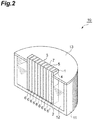
Figure 2] Figure 2 is a longitudinal cross-sectional view of the EFG-based crucible and the die for EFG-based single crystal growth inFigure 1 . - [
Figure 3] Figure 3 is a plan view of the die for EFG-based single crystal growth according to the embodiment. - [
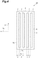
Figure 4] Figure 4 is a plan view of a conventional die for EFG-based single crystal growth. - [
Figure 5] Figure 5 is a table illustrating specifications of the die for EFG-based single crystal growth according to an example. - [
Figure 6] Figure 6 is a table illustrating specifications of a die for EFG-based single crystal growth according to a comparative example. - [
Figure 7] Figure 7 is a graph illustrating an impurity concentration of the EFG-based single crystal according to the example. - [
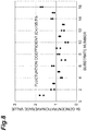
Figure 8] Figure 8 is a graph illustrating an impurity concentration of an EFG-based single crystal according to the comparative example. - Hereinafter, an embodiment of the present invention will be described in detail with reference to the accompanying drawings. A die for EFG-based single crystal growth and an EFG-based single crystal growth method according to the present embodiment are intended to grow, for example, a β-Ga2O3 single crystal using an EFG method. As shown in
Figure 1 andFigure 2 , an EFG-based singlecrystal manufacturing apparatus 10 is provided with acrucible 11 accommodating araw material melt 12 based on Ga2O3 or the like, adie 1 for EFG-based single crystal growth installed in thecrucible 11, alid 13 covering an upper surface of thecrucible 11 except anupper surface 5 of thedie 1, aseed crystal holder 16 holding aseed crystal 15 based on Ga2O3 or the like and ashaft 17 liftably supporting theseed crystal holder 16. - The
crucible 11 is heated by heating means (not shown) and heated up to, for example, 1800°C or higher exceeding a melting point of β-Ga2O3. A solid raw material based on Ga2O3 or the like having an additive concentration of 0.016 mol% of an additive such as Sn accommodated in thecrucible 11 is melted in a heating process and converts to theraw material melt 12 based on Ga2O3 or the like. Thecrucible 11 and the die 1 for EFG-based single crystal growth are made of iridium-based metal materials having heat resistance capable of accommodating theraw material melt 12 based on Ga2O3 or the like. Thelid 13 prevents theraw material melt 12 based on Ga2O3 or the like from evaporating from thecrucible 11 and further prevents a vapor of theraw material melt 12 based on Ga2O3 or the like from adhering to theseed crystal 15 based on Ga2O3 or the like. - The
die 1 for EFG-based single crystal growth is provided with alower surface 2 to be immersed into theraw material melt 12 based on Ga2O3 or the like with an impurity such as Sn added, the rectangularupper surface 5 facing theseed crystal 15 based on Ga2O3 or the like and having along side 3 and ashort side 4 shorter than thelong side 3, and a plurality ofslit sections 6 extending from thelower surface 2 to theupper surface 5 and causing theraw material melt 12 to ascend from thelower surface 2 to theupper surface 5. Note that examples of the rectangularupper surface 5 include a surface in which corners formed of thelong side 3 and theshort side 4 of theupper surface 5 form angles other than exact 90° and a surface in which corners are rounded. - As shown in
Figure 1 ,Figure 2 andFigure 3 ,openings 7 of the plurality ofslit sections 6 on theupper surface 5 each have a rectangular shape, and alongitudinal direction 71 and atraverse direction 7s. The respectivelongitudinal directions 71 of theopenings 7 of the plurality ofslit sections 6 on theupper surface 5 are parallel to one another and non-parallel to thelong side 3 of theupper surface 5. More specifically, the respectivelongitudinal directions 71 of theopenings 7 of the plurality ofslit sections 6 on theupper surface 5 are parallel to theshort side 4 of theupper surface 5. Note that examples of therectangular openings 7 also include a case where corners formed of thelongitudinal direction 71 and thetraverse direction 7s of the opening 7 form an angle other than exact 90° and a case where the corners are rounded. - As shown in
Figure 3 , a distance α of theopening 7 of theslit section 6 on theupper surface 5 in which theopening 7 on theupper surface 5 is most proximate to anouter edge 5e of theupper surface 5 among the plurality ofslit sections 6 from theouter edge 5e of theupper surface 5 is 2 mm or less. Intervals β betweencenter lines 7c in thelongitudinal direction 71 of theopenings 7 of the neighboringslit sections 6 on theupper surface 5 are equal and are 2 mm or less. Respective lengths γ in thetraverse direction 7s of theopenings 7 of the plurality ofslit sections 6 on theupper surface 5 is 2 mm or less. Respective intervals δ between theopenings 7 of the neighboringslit sections 6 on theupper surface 5 are equal and are 2 mm or less. Note that the interval β and the interval δ between theopenings 7 of theslit sections 6 need not always be equal. - Hereinafter, an EFG-based single crystal growth method using the
die 1 for EFG-based single crystal growth of the present embodiment will be described. As shown inFigure 2 , thedie 1 for single crystal growth is installed in thecrucible 11 so that thelower surface 2 of thedie 1 is accommodated in thecrucible 11 and is immersed into theraw material melt 12 based on Ga2O3 or the like with an impurity such as Sn added. Due to a capillary phenomenon, theraw material melt 12 based on Ga2O3 or the like ascends in theslit sections 6 and reaches theupper surface 5 of thedie 1. - An output of heating means (not shown) is adjusted so that the temperature of the
upper surface 5 of thedie 1 becomes a temperature suitable for growth. As shown inFigure 1 , theshaft 17 is caused to descend and theseed crystal 15 based on Ga2O3 or the like held by theseed crystal holder 16 comes into contact with theraw material melt 12 based on Ga2O3 or the like, which has reached theupper surface 5 of thedie 1. Theshaft 17 is caused to ascend and raise theseed crystal 15 based on Ga2O3 or the like in contact with theraw material melt 12 based on Ga2O3 or the like, thus causing asingle crystal 14 based on Ga2O3 or the like to grow in a growth direction D from theupper surface 5 of thedie 1. - According to the EFG-based single crystal growth method using the
die 1 for EFG-based single crystal growth of the above present embodiment, the EFG-basedsingle crystal 14 is grown, thesingle crystal 14 having, for example, an impurity concentration fluctuation coefficient of 30% or less in the region excluding a distance range of 1 mm from an outer edge of a cross section orthogonal to the growth direction D of thesingle crystal 14. - According to the present embodiment, the
die 1 for EFG-based single crystal growth comprises thelower surface 2 to be immersed into theraw material melt 12 with an impurity added, the rectangularupper surface 5 facing theseed crystal 15 and having thelong side 3 and theshort side 4 shorter than thelong side 3, and the plurality ofslit sections 6 extending from thelower surface 2 to theupper surface 5 and causing theraw material melt 12 to ascend from thelower surface 2 to theupper surface 5. The respectivelongitudinal directions 71 ofopenings 7 of the plurality ofslit sections 6 on theupper surface 5 are parallel to one another and non-parallel to thelong side 3 of theupper surface 5. Therefore, if total areas of theopenings 7 ofslit sections 6 are same, the interval δ between theopenings 7 of the neighboringslit sections 6 is shorter than the interval when the respectivelongitudinal directions 71 of theopenings 7 of theslit sections 6 on theupper surface 5 are parallel to thelong side 3 of theupper surface 5, and impurity segregation is less likely to occur between therespective slit sections 6, and so it is possible to improve uniformity of an impurity concentration of the grownsingle crystal 14. - According to the present embodiment, since the respective
longitudinal directions 71 of theopenings 7 of the plurality ofslit sections 6 on theupper surface 5 are parallel to theshort side 4 of theupper surface 5, the respective intervals δ between theopenings 7 of the neighboringslit sections 6 are shorter than the interval when the respectivelongitudinal directions 71 of theopenings 7 of theslit sections 6 on theupper surface 5 are parallel to thelong side 3 of theupper surface 5, and it is thereby possible to improve uniformity of an impurity concentration of the grownsingle crystal 14. Furthermore, since the length of thelongitudinal direction 71 of theopening 7 of theslit section 6 on theupper surface 5 is shorter than the length when the respectivelongitudinal directions 71 of theopenings 7 of theslit sections 6 on theupper surface 5 are parallel to thelong side 3 of theupper surface 5, thedie 1 is less likely to deform and durability of thedie 1 can be improved. - According to the present embodiment, the distance α of the
opening 7 of theslit section 6 on theupper surface 5 in which theopening 7 on theupper surface 5 is most proximate to theouter edge 5e of theupper surface 5 among the plurality ofslit sections 6 from theouter edge 5e is 2 mm or less, and it is thereby possible to expand the region where the impurity concentration of the grownsingle crystal 14 is made uniform. - As described, for example, in paragraph (0006) of
Patent Literature 1, according to the prior art in which the respective longitudinal directions of the openings of the plurality of slits on the upper surface of the die are parallel to the long side of the rectangular upper surface of the die, a warp is produced when the thickness of the plate member constituting the die is 1 mm or less, and accurate manufacturing of the die requires a plate member having a thickness of 2.4 mm or more. That is, according to the prior art, the plate member constituting a widest side face of the die extending over a long distance in the direction parallel to the long side of the upper surface of the die is supported only at two locations, at both ends on the short side of the upper surface of the die, and therefore the mechanical strength of the die is low and the thickness of the plate member needs to be increased. Therefore, it is difficult for the prior art to set the distance α to 2 mm or less. - On the other hand, according to the present embodiment, the plate member constituting the widest side face of the
die 1 extending over a long distance in the direction parallel to thelong side 3 of theupper surface 5 of thedie 1 is also supported by the plate members partitioning therespective slit sections 6 in addition to the two locations, at both ends on theshort side 4 of thedie 1. That is, in the present embodiment, the plate members constituting the widest side face of thedie 1 are supported at many supporting points and the supporting points are distributed over theentire die 1, and so the mechanical strength of theentire die 1 improves and thedie 1 can be manufactured accurately even using thin plate members. - According to the present embodiment, since the interval β between the
center lines 7c in thelongitudinal direction 71 of theopenings 7 of the neighboringslit sections 6 on theupper surface 5 is 2 mm or less, it is possible to further improve impurity concentration uniformity of the grownsingle crystal 14. - Regarding the plate members partitioning the respective slit sections, according to the prior art described in
Patent Literature 1, the plate members partitioning the respective slit sections are supported only at two locations, at both ends on the short side of the upper surface of the die and extend in a direction parallel to the long side of the upper surface of the die over a long distance, and so an influence when a warp is produced in the plate members partitioning the respective slit sections is considerably large and the thickness of the plate members needs to be increased to prevent warpage. Therefore, it is difficult for the prior art to set the interval β to 2 mm or less. - On the other hand, according to the present embodiment, the distance between the two locations at both ends of the plate members at which the plate members partitioning the
respective slit sections 6 are supported is the distance in a direction parallel to theshort side 4, which is shorter than the distance in the direction parallel to thelong side 3 of theupper surface 5 of theconventional die 1, and so even when a warp of the same radius of curvature is produced, the influence of the warp is minimal and it is possible to reduce the thickness of the plate members partitioning therespective slit sections 6. - According to the present embodiment, the respective lengths γ in the
traverse direction 7s of theopenings 7 of the plurality ofslit sections 6 on theupper surface 5 are 2 mm or less, and so it is possible to increase the height by which theslit sections 6 cause theraw material melt 12 to ascend from thelower surface 2 to theupper surface 5. - According to the present embodiment, it is possible to grow the
single crystal 14 in which impurity concentration uniformity is improved using the EFG method. Furthermore, according to the present embodiment, it is possible to provide thesingle crystal 14 in which impurity concentration uniformity is improved and characteristics are made more uniform. - Although the embodiment of the present invention has been described so far, the present invention is not limited to the above embodiment but can be implemented in various modes. For example, the shape and arrangement of the
openings 7 of the plurality ofslit sections 6 on theupper surface 5 can be changed as appropriate. - The Ga2O3-based
single crystal 14 with Sn added as an impurity was grown using the aforementioned EFG-based singlecrystal manufacturing apparatus 10 and die 1 for EFG-based single crystal growth. Dimensions or quantities of the respective regions of thedie 1 are as shown inFigure 5 . Portions of the Ga2O3-basedraw material melt 12 caused to ascend through the plurality ofslit sections 6 formed in thedie 1 for single crystal growth were united and spread over theupper surface 5 of thedie 1, and a thick plate-like Ga2O3-basedsingle crystal 14 having a cross-sectional shape of a straight barrel portion of approximately 57 mm in width, approximately 18 mm in thickness and approximately 112 mm in length was grown. - The straight barrel portion was cut out from the grown
single crystal 14, divided in two at a cross section intersecting in a length direction (growth direction D), each of the two single crystal blocks having a thickness of approximately 18 mm obtained was cut into 18 flat plates so that the cutting surfaces cut by a multi-saw were parallel to the main surface of the crystal. After each of the two single crystal blocks was cut into the 18 flat plates, both surfaces of the respective flat plates were then polished and 36 single crystal substrates having a thickness of 0.4 mm were manufactured from onesingle crystal 14. - Sn concentrations of 32 single crystal substrates obtained by excluding 4 single crystal substrates located on an outermost side of the
single crystal 14 during single crystal growth and having low crystallinity from the 36 single crystal substrates obtained were measured using SIMS (Secondary Ion Mass Spectrometry). That is, concentrations of Sn, which was an impurity, in the region obtained by excluding a distance range of 1 mm from the outer edge of a cross section orthogonal to the growth direction D of thesingle crystal 14 were measured. The measurement results are shown inFigure 7 . The abscissa of a graph inFigure 7 represents order of the single crystal substrates in the thickness direction obtained by cutting the Ga2O3-basedsingle crystal 14 grown into a thick plate shape in parallel with the main surface of the crystal. The ordinate of the graph inFigure 7 represents a value obtained by dividing the respective measured values of Sn concentrations of the 32 single crystal substrates by an average value of Sn concentrations of the 32 substrates. A fluctuation coefficient (Cv) of the 32 single crystal substrates, that is, a value obtained by dividing a standard deviation of Sn concentrations by the average value was 12.1%, which is equal to or less than 30%. That is, it is seen that the impurity concentration of thesingle crystal 14 grown by thedie 1 in the example exhibits a high level of uniformity. - Although growth of the above
single crystal 14 was repeated 12 times or more, no significant change in shape in thedie 1 for single crystal growth was observed. That is, it is seen that thedie 1 for single crystal growth hardly deforms and has excellent durability as well. - A plan view of a
die 20 for single crystal growth used as a comparative example is shown inFigure 4 . In thedie 20, the respectivelongitudinal directions 71 of theopenings 7 of the plurality ofslit sections 6 on theupper surface 5 are parallel to thelong side 3 of theupper surface 5. The interval β and the interval δ are equal among theopenings 7 of theslit sections 6. Dimensions or quantities of the respective regions of the die 20 are as shown inFigure 6 . Thesingle crystal 14 was grown under completely the same conditions as the conditions in the example except for thedie 20 for single crystal growth and 36 single crystal substrates were finally manufactured after being polished to have a thickness of 0.4 mm from one single crystal. - Sn concentrations of 32 single crystal substrates obtained by excluding 4 single crystal substrates located on an outermost side of the
single crystal 14 during single crystal growth and having low crystallinity from the 36 single crystal substrates obtained were measured using SIMS. That is, concentrations of Sn, which was an impurity, in the region obtained by excluding a distance range of 1 mm from the outer edge of a cross section orthogonal to the growth direction D of thesingle crystal 14 were measured. The measurement results are shown inFigure 8 . The abscissa of a graph inFigure 8 represents order of the single crystal substrates in the thickness direction obtained by cutting the Ga2O3-basedsingle crystal 14 grown into a thick plate shape in parallel with the main surface of the crystal. The ordinate of the graph inFigure 8 represents a value obtained by dividing the respective measured values of Sn concentrations of the 32 single crystal substrates by an average value of Sn concentrations of the 32 substrates. A fluctuation coefficient (Cv) of the 32 single crystal substrates, that is, a value obtained by dividing a standard deviation of Sn concentrations by the average value was 35.5%, which exceeds 30%. That is, it is seen that the impurity concentration of thesingle crystal 14 grown by the die 20 in the comparative example exhibits a low level of uniformity. - From a point in time at which growth of the above
single crystal 14 was repeated 6 times, a distortion was observed in a middle part on theupper surface 5 of thedie 20 for single crystal growth, and from the ninth growth onward, the amount of the Ga2O3-basedraw material melt 12 supplied from the center of theslit sections 6 decreased in theopenings 7 of theslit sections 6 located outside and the Ga2O3-basedraw material melt 12 no longer became wet or spread over the entireupper surface 5 of thedie 20. That is, it is seen that theconventional die 20 for single crystal growth is easily deformed and is inferior in durability to thedie 1 in the example. - According to the die for EFG-based single crystal growth, the EFG-based single crystal growth method and the EFG-based single crystal of the present invention, it is possible to improve impurity concentration uniformity of a grown single crystal.
- 1 ··· die, 2 ··· lower surface, 3 ··· long side, 4 ··· short side, 5 ··· upper surface, 5e ··· outer edge, 6 ··· slit section, 7 ··· opening, 71 ··· longitudinal direction, 7s ··· traverse direction, 7c ··· center line, 10 ··· single crystal manufacturing apparatus, 11 ··· crucible, 12 ··· raw material melt, 13 ··· lid, 14 ··· single crystal, 15 ··· seed crystal, 16 ··· seed crystal holder, 17 ··· shaft, 20 ··· die, D ··· growth direction, α ··· distance, β ··· interval, γ ··· length, δ ··· interval
Claims (7)
- A die for EFG-based single crystal growth comprising:a lower surface to be immersed into a raw material melt with an impurity added;a rectangular upper surface facing a seed crystal and having a long side and a short side shorter than the long side; anda plurality of slit sections extending from the lower surface to the upper surface and causing the raw material melt to ascend from the lower surface to the upper surface, whereinrespective longitudinal directions of openings of the plurality of slit sections on the upper surface are parallel to one another and non-parallel to the long side of the upper surface.
- The die for EFG-based single crystal growth according to claim 1, wherein the respective longitudinal directions of the openings of the plurality of slit sections on the upper surface are parallel to the short side of the upper surface.
- The die for EFG-based single crystal growth according to claim 1 or 2, wherein a distance of the opening of the slit section on the upper surface in which the opening on the upper surface is most proximate to an outer edge of the upper surface, among the plurality of slit sections, from the outer edge of the upper surface is 2 mm or less.
- The die for EFG-based single crystal growth according to any one of claims 1 to 3, wherein an interval between center lines in the longitudinal direction of the openings of the neighboring slit sections on the upper surface is 2 mm or less.
- The die for EFG-based single crystal growth according to any one of claims 1 to 4, wherein respective lengths in a traverse direction of the openings of the plurality of slit sections on the upper surface is 2 mm or less.
- An EFG-based single crystal growth method using the die for EFG-based single crystal growth according to any one of claims 1 to 5.
- An EFG-based single crystal grown using the EFG-based single crystal growth method according to claim 6, wherein an impurity concentration fluctuation coefficient is 30% or less in a region excluding a distance range of 1 mm from an outer edge of a cross section orthogonal to a growth direction of the single crystal.
Applications Claiming Priority (2)
| Application Number | Priority Date | Filing Date | Title |
|---|---|---|---|
| JP2018056165A JP7147213B2 (en) | 2018-03-23 | 2018-03-23 | Single crystal growth die by EFG method, single crystal growth method by EFG method and single crystal by EFG method |
| PCT/JP2019/002551 WO2019181197A1 (en) | 2018-03-23 | 2019-01-25 | Die for efg-based single crystal growth, efg-based single crystal growth method, and efg single crystal |
Publications (2)
| Publication Number | Publication Date |
|---|---|
| EP3770307A1 true EP3770307A1 (en) | 2021-01-27 |
| EP3770307A4 EP3770307A4 (en) | 2022-01-12 |
Family
ID=67987597
Family Applications (1)
| Application Number | Title | Priority Date | Filing Date |
|---|---|---|---|
| EP19771196.3A Pending EP3770307A4 (en) | 2018-03-23 | 2019-01-25 | Die for efg-based single crystal growth, efg-based single crystal growth method, and efg single crystal |
Country Status (6)
| Country | Link |
|---|---|
| US (1) | US11492724B2 (en) |
| EP (1) | EP3770307A4 (en) |
| JP (1) | JP7147213B2 (en) |
| CN (1) | CN111836920A (en) |
| TW (1) | TWI759587B (en) |
| WO (1) | WO2019181197A1 (en) |
Families Citing this family (1)
| Publication number | Priority date | Publication date | Assignee | Title |
|---|---|---|---|---|
| JP7436978B2 (en) * | 2019-10-28 | 2024-02-22 | Agc株式会社 | Single crystal ingot, crystal growth die, and method for manufacturing single crystal |
Family Cites Families (10)
| Publication number | Priority date | Publication date | Assignee | Title |
|---|---|---|---|---|
| JPS5373480A (en) | 1976-12-13 | 1978-06-29 | Nippon Telegr & Teleph Corp <Ntt> | Hot zone for sheet crystal making apparatus |
| US4647437A (en) | 1983-05-19 | 1987-03-03 | Mobil Solar Energy Corporation | Apparatus for and method of making crystalline bodies |
| US5458083A (en) * | 1992-05-29 | 1995-10-17 | Chichibu Cement Co., Ltd. | Growth method for a rod form of single oxide crystal |
| JP2012229134A (en) | 2011-04-25 | 2012-11-22 | Fujikura Ltd | Method for producing oxide eutectic body |
| JP5891028B2 (en) | 2011-12-16 | 2016-03-22 | 株式会社タムラ製作所 | Method for producing Ga2O3-based substrate |
| CN104220650A (en) * | 2012-05-16 | 2014-12-17 | 并木精密宝石株式会社 | Monocrystalline gallium oxide and monocrystalline gallium oxide substrate |
| JP5865867B2 (en) * | 2013-05-13 | 2016-02-17 | 株式会社タムラ製作所 | Method for growing β-Ga 2 O 3 single crystal and method for producing β-Ga 2 O 3 single crystal substrate |
| JP5749839B1 (en) * | 2014-06-30 | 2015-07-15 | 株式会社タムラ製作所 | β-Ga2O3-based single crystal substrate |
| JP5895280B1 (en) | 2014-09-19 | 2016-03-30 | 並木精密宝石株式会社 | Method for producing a plurality of sapphire single crystals |
| JP2017193472A (en) | 2016-04-22 | 2017-10-26 | 並木精密宝石株式会社 | Crystal growth equipment for EFG method |
-
2018
- 2018-03-23 JP JP2018056165A patent/JP7147213B2/en active Active
-
2019
- 2019-01-25 CN CN201980018372.8A patent/CN111836920A/en active Pending
- 2019-01-25 US US16/982,280 patent/US11492724B2/en active Active
- 2019-01-25 EP EP19771196.3A patent/EP3770307A4/en active Pending
- 2019-01-25 WO PCT/JP2019/002551 patent/WO2019181197A1/en not_active Ceased
- 2019-03-18 TW TW108109155A patent/TWI759587B/en active
Also Published As
| Publication number | Publication date |
|---|---|
| JP2019167267A (en) | 2019-10-03 |
| US20210017668A1 (en) | 2021-01-21 |
| US11492724B2 (en) | 2022-11-08 |
| CN111836920A (en) | 2020-10-27 |
| TW201940757A (en) | 2019-10-16 |
| JP7147213B2 (en) | 2022-10-05 |
| TWI759587B (en) | 2022-04-01 |
| WO2019181197A1 (en) | 2019-09-26 |
| EP3770307A4 (en) | 2022-01-12 |
Similar Documents
| Publication | Publication Date | Title |
|---|---|---|
| US10526721B2 (en) | Method for growing β-GA2O3-based single crystal | |
| US20150308012A1 (en) | METHOD FOR GROWING B-Ga2O3 SINGLE CRYSTAL | |
| DE112012002192T5 (en) | A silicon carbide substrate, silicon carbide ingot, and a method of manufacturing a silicon carbide substrate and a silicon carbide ingot | |
| US11319646B2 (en) | Gallium arsenide single crystal substrate | |
| US10569317B2 (en) | Single-crystal diamond, tool using same, and method of producing single-crystal diamond | |
| EP2851458A1 (en) | Monocrystalline gallium oxide and monocrystalline gallium oxide substrate | |
| KR102766961B1 (en) | SiC SUBSTRATE AND SiC INGOT | |
| EP2775015A1 (en) | SiC SINGLE CRYSTAL MANUFACTURING METHOD | |
| US11492724B2 (en) | Die for EFG-based single crystal growth, EFG-based single crystal growth method, and EFG single crystal | |
| US20130061801A1 (en) | Method for manufacturing silicon carbide crystal | |
| US7883998B2 (en) | Vapor phase growth method | |
| JP7536916B2 (en) | Single crystal | |
| CN112831832B (en) | A mold and growth method for growing gallium oxide single crystal by guided mode method | |
| JP2000313699A (en) | Method for producing semi-insulating InP single crystal | |
| EP4053310A1 (en) | Single crystal ingot, crystal growth die, and single crystal production method | |
| KR20250103415A (en) | SiC INGOT AND METHOD FOR MANUFACTURING SiC SUBSTRATE | |
| TW202424291A (en) | Single crystal silicon substrate for heteroepitaxial growth, epitaxial substrate, semiconductor device, and method for manufacturing single crystal silicon substrate for heteroepitaxial growth | |
| JP2014205618A (en) | β-Ga2O3-BASED SINGLE CRYSTAL AND SUBSTRATE | |
| JP2014503452A (en) | Method for reducing the resistivity range of semiconductor crystalline sheets grown in a multi-lane furnace. | |
| KR20200042516A (en) | Single crystal of silicon having <100> orientation doped with n-type dopant and method for manufacturing such single crystal | |
| JPH02196085A (en) | Liquid phase epitaxial growth method | |
| JP2010165937A (en) | Method of manufacturing epitaxial wafer, and graphite tool |
Legal Events
| Date | Code | Title | Description |
|---|---|---|---|
| STAA | Information on the status of an ep patent application or granted ep patent |
Free format text: STATUS: THE INTERNATIONAL PUBLICATION HAS BEEN MADE |
|
| PUAI | Public reference made under article 153(3) epc to a published international application that has entered the european phase |
Free format text: ORIGINAL CODE: 0009012 |
|
| STAA | Information on the status of an ep patent application or granted ep patent |
Free format text: STATUS: REQUEST FOR EXAMINATION WAS MADE |
|
| 17P | Request for examination filed |
Effective date: 20201002 |
|
| AK | Designated contracting states |
Kind code of ref document: A1 Designated state(s): AL AT BE BG CH CY CZ DE DK EE ES FI FR GB GR HR HU IE IS IT LI LT LU LV MC MK MT NL NO PL PT RO RS SE SI SK SM TR |
|
| AX | Request for extension of the european patent |
Extension state: BA ME |
|
| DAV | Request for validation of the european patent (deleted) | ||
| DAX | Request for extension of the european patent (deleted) | ||
| A4 | Supplementary search report drawn up and despatched |
Effective date: 20211209 |
|
| RIC1 | Information provided on ipc code assigned before grant |
Ipc: C30B 29/64 20060101ALI20211203BHEP Ipc: C30B 29/16 20060101ALI20211203BHEP Ipc: C30B 15/34 20060101AFI20211203BHEP |