EP3769347B1 - Vertikale josephson-kontaktvorrichtung - Google Patents
Vertikale josephson-kontaktvorrichtung Download PDFInfo
- Publication number
- EP3769347B1 EP3769347B1 EP19708811.5A EP19708811A EP3769347B1 EP 3769347 B1 EP3769347 B1 EP 3769347B1 EP 19708811 A EP19708811 A EP 19708811A EP 3769347 B1 EP3769347 B1 EP 3769347B1
- Authority
- EP
- European Patent Office
- Prior art keywords
- superconducting layer
- superconductor
- substrate
- device structure
- chip surface
- Prior art date
- Legal status (The legal status is an assumption and is not a legal conclusion. Google has not performed a legal analysis and makes no representation as to the accuracy of the status listed.)
- Active
Links
Images


Classifications
-
- B—PERFORMING OPERATIONS; TRANSPORTING
- B82—NANOTECHNOLOGY
- B82Y—SPECIFIC USES OR APPLICATIONS OF NANOSTRUCTURES; MEASUREMENT OR ANALYSIS OF NANOSTRUCTURES; MANUFACTURE OR TREATMENT OF NANOSTRUCTURES
- B82Y10/00—Nanotechnology for information processing, storage or transmission, e.g. quantum computing or single electron logic
-
- H—ELECTRICITY
- H03—ELECTRONIC CIRCUITRY
- H03K—PULSE TECHNIQUE
- H03K19/00—Logic circuits, i.e. having at least two inputs acting on one output; Inverting circuits
- H03K19/02—Logic circuits, i.e. having at least two inputs acting on one output; Inverting circuits using specified components
- H03K19/195—Logic circuits, i.e. having at least two inputs acting on one output; Inverting circuits using specified components using superconductive devices
-
- H—ELECTRICITY
- H10—SEMICONDUCTOR DEVICES; ELECTRIC SOLID-STATE DEVICES NOT OTHERWISE PROVIDED FOR
- H10N—ELECTRIC SOLID-STATE DEVICES NOT OTHERWISE PROVIDED FOR
- H10N60/00—Superconducting devices
- H10N60/01—Manufacture or treatment
- H10N60/0912—Manufacture or treatment of Josephson-effect devices
-
- H—ELECTRICITY
- H10—SEMICONDUCTOR DEVICES; ELECTRIC SOLID-STATE DEVICES NOT OTHERWISE PROVIDED FOR
- H10N—ELECTRIC SOLID-STATE DEVICES NOT OTHERWISE PROVIDED FOR
- H10N60/00—Superconducting devices
- H10N60/10—Junction-based devices
- H10N60/12—Josephson-effect devices
-
- H—ELECTRICITY
- H10—SEMICONDUCTOR DEVICES; ELECTRIC SOLID-STATE DEVICES NOT OTHERWISE PROVIDED FOR
- H10N—ELECTRIC SOLID-STATE DEVICES NOT OTHERWISE PROVIDED FOR
- H10N60/00—Superconducting devices
- H10N60/10—Junction-based devices
- H10N60/128—Junction-based devices having three or more electrodes, e.g. transistor-like structures
-
- H—ELECTRICITY
- H10—SEMICONDUCTOR DEVICES; ELECTRIC SOLID-STATE DEVICES NOT OTHERWISE PROVIDED FOR
- H10N—ELECTRIC SOLID-STATE DEVICES NOT OTHERWISE PROVIDED FOR
- H10N60/00—Superconducting devices
- H10N60/80—Constructional details
- H10N60/85—Superconducting active materials
-
- H—ELECTRICITY
- H10—SEMICONDUCTOR DEVICES; ELECTRIC SOLID-STATE DEVICES NOT OTHERWISE PROVIDED FOR
- H10N—ELECTRIC SOLID-STATE DEVICES NOT OTHERWISE PROVIDED FOR
- H10N69/00—Integrated devices, or assemblies of multiple devices, comprising at least one superconducting element covered by group H10N60/00
-
- B—PERFORMING OPERATIONS; TRANSPORTING
- B82—NANOTECHNOLOGY
- B82Y—SPECIFIC USES OR APPLICATIONS OF NANOSTRUCTURES; MEASUREMENT OR ANALYSIS OF NANOSTRUCTURES; MANUFACTURE OR TREATMENT OF NANOSTRUCTURES
- B82Y40/00—Manufacture or treatment of nanostructures
-
- H—ELECTRICITY
- H10—SEMICONDUCTOR DEVICES; ELECTRIC SOLID-STATE DEVICES NOT OTHERWISE PROVIDED FOR
- H10N—ELECTRIC SOLID-STATE DEVICES NOT OTHERWISE PROVIDED FOR
- H10N60/00—Superconducting devices
- H10N60/80—Constructional details
- H10N60/805—Constructional details for Josephson-effect devices
Definitions
- the subject invention relates generally to superconducting devices, and more specifically, to fabricating a vertical Josephson junction superconducting device using a silicon-on-metal (SOM) substrate.
- SOM silicon-on-metal
- Quantum computing is generally the use of quantum-mechanical phenomena for the purpose of performing computing and information processing functions. Quantum computing can be viewed in contrast to classical computing, which generally operates on binary values with transistors. That is, while classical computers can operate on bit values that are either 0 or 1, quantum computers operate on quantum bits that comprise superpositions of both 0 and 1, can entangle multiple quantum bits, and use interference to obtain computational results.
- Quantum computing hardware can be different from classical computing hardware.
- superconducting quantum circuits generally rely on Josephson junctions, which can be fabricated in a semiconductor device.
- a Josephson junction generally manifests the Josephson effect of a supercurrent, where current can flow indefinitely across a Josephson junction without an applied voltage.
- a Josephson junction can be created by weakly coupling two superconductors (a material that conducts electricity without resistance), for example, by a tunnel barrier as described below.
- Some prior art Josephson junctions can be implemented using shadow evaporation.
- a problem with fabricating prior art Josephson junctions using shadow evaporation can be that this approach is not scalable, because shadow evaporation can produce non-uniform results on larger substrates, such as 200 mm or 300 mm wafers.
- Josephson junctions implemented via shadow evaporation can have high variability of the supercurrent.
- Josephson junctions implemented via shadow evaporation can be made with a lift-off process, which, in turn, can cause flares at the edges of a remaining superconducting layer, can allow for one or more floating superconducting islands to be formed near a Josephson junction (where using undercut in resist, or hard mask, profile); and can have some junction variability (which causes variability of the critical current) caused by undercut and small misalignments in tilted evaporation. Additionally, a problem with shadow evaporation is that a number of choices for both materials and deposition approaches can be limited.
- Josephson junctions used in single flux quantum (SFQ) computing which can be vertical, but can have a problem of having an associated loss beyond what is suitable for quantum computing.
- This associated loss with a SFQ junction can include both loss due to surrounding dielectrics with insufficient loss tangent, and loss in tunnel barrier.
- a SFQ junction generally has a larger area than a quantum bit (qubit) junction.
- a chip surface base device structure according to claim 1 is provided.
- the tunnel barrier layer is located on at least one of the first superconducting layer, or a second superconducting layer that is coupled with the first superconducting layer.
- the method further comprises depositing a second superconducting layer between the first superconducting layer and the tunnel barrier layer.
- An advantage of depositing the second superconducting layer in this manner can be that a height of the second superconducting layer can be used to set a height of the tunnel base layer in the via.
- An advantage of a chip surface base device structure according to the invention can be that it contains vertical Josephson junctions that are more uniform than Josephson junctions from previous techniques.
- the tunnel barrier layer is formed on the superconducting layer.
- the present disclosure can be implemented to produce a vertical Josephson junction computing device that provides a solution to one or more of those problems.
- a vertical Josephson junction computing device can have an advantage of improved scaling because of a reduced footprint relative to that of a non-vertical Josephson junction device.
- Such a vertical Josephson junction computing device can also have an advantage of providing more choices in both materials and deposition methods relative to a number of choices for a shadow evaporated overlap Josephson junction.
- Such a vertical Josephson junction computing device can have an advantage of fabrication scaling because the device is compatible with chip manufacturing approaches. Additionally, such a vertical Josephson junction computing device can have an advantage of being embedded in a very low loss environment.
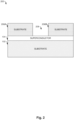
- FIG. 1 illustrates a chip surface base device structure in accordance with one or more embodiments described herein.
- chip surface base device structure 100 comprises substrate 102, superconductor 104, and substrate 106.
- a chip surface base device structure can sometimes be referred to as a chip surface base device structure.
- Chip surface base device structure 100 can be considered to be a buried metal flow, where the metal is a superconducting material.
- the top substrate layer - substrate 106 - can be ground to a thickness of approximately 100-200 nm, either before or after substrate 106, superconductor 104, and substrate 102 are physically coupled together (as opposed to an electrical coupling, such as between two capacitive plates).
- superconductor 104 can be titanium (Ti), tantalum (Ta), tungsten (W), or titanium nitride (TiN).
- substrate 102 and substrate 106 can have initial thicknesses of approximately 500 micrometers ( ⁇ m) to 800 ⁇ m. Then, in some examples, the various materials used can be used in temperatures up to approximately 500 degrees Celsius (C). In some examples, materials with lower melting points, such as aluminum (Al) can be used, and these materials can begin to deform at approximately 300 C.
- C degrees Celsius
- one or both of substrate 102 and substrate 106 can be crystalline silicon (Si), and such a substrate can be referred to as a crystalline silicon substrate.
- crystalline Si can improve a coherence time of a qubit associated with a vertical Josephson junction as described herein.
- a high-resistivity crystalline Si can be utilized, which can further improve coherence time. In some examples, this crystalline Si can be grown.
- a portion of superconductor 104 is deposited onto substrate 102, and a portion of superconductor 104 is deposited onto substrate 106. Then, these two portions of superconductor 104 can be bonded together to connect substrate 102 to superconductor 104 to substrate 106. Put another way, after depositing the respective portions of superconductor 104 on substrate 102 and substrate 106, respectively, the exposed surface of a first portion of superconductor 104 can then be bonded to the exposed surface of a second portion of superconductor 104. In some examples, bonding can be effectuated with a low-temperature anneal, or another adhesion approach.
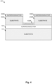
- FIG. 2 illustrates the chip surface base device structure of FIG. 1 after creation of via 208 in accordance with one or more embodiments described herein.
- chip surface base device structure 200 reflects etching a via into substrate 106 of chip surface base device structure 100.
- a via 208 can generally comprise an opening through a layer of a chip base surface, through which a conductive connection between two other layers can be formed.
- chip surface base device structure 100 has substrate 106, here substrate 106 has been etched to form via 208, leaving substrate 206A and substrate 206B to remain from what was substrate 106 (with via 208 formed between substrate 206A and substrate 206B).
- the cross-sectional side view of chip surface base device structure 200 shows that substrate 206A and substrate 206B are separated.
- via 208 can extend into the superconductor 104, meaning part of the top of superconductor 104 may be removed at the location of via 208.
- etch lithography can be implemented to etch via 208, with a depth of the via of 100-200 nm.
- an aspect ratio of 1:1 between a height and a width of a via can be effectuated.
- FIG. 3 illustrates the chip surface base device structure of FIG. 2 after depositing a tunnel barrier layer in accordance with one or more embodiments described herein.
- a tunnel barrier layer has been deposited on chip surface base device structure 200, and this tunnel barrier layer comprises tunnel barrier 308A, tunnel barrier 308B, and tunnel barrier 308C.
- tunnel barrier 308A, tunnel barrier 308B, and tunnel barrier 308C can be deposited on chip surface base device structure 200 using a sputter approach, an evaporative approach, or an atomic layer deposition (ALD) approach.
- tunnel barrier 308A, tunnel barrier 308B, and tunnel barrier 308C can be aluminum oxide (Al 2 O 3 ), a non-superconducting metal (sometimes referred to as a "normal" metal), an oxide or a nitride.
- the tunnel barrier 308B can be grown or chemically induced on the exposed surface (after etch) of superconductor 104, for example, by oxidation.
- the surface layers of tunnel barrier 308A and tunnel barrier 308C may or may not exist.
- a tunnel barrier layer can be a thin layer of non-conducting material.
- chip surface base device structure 300 can further produce a chip surface base device structure, similar to those described with respect to FIGS. 4-11 .
- a difference between a chip surface base device structure created using chip surface base device structure 300 and a chip surface base device structure using chip surface base device structure 400 can be found in the presence of a second superconducting layer.
- a second superconducting layer is deposited below a tunnel barrier layer, and this second superconducting layer is omitted from chip surface base device structure 300.
- An advantage of depositing or growing the tunnel barrier layer on the first superconducting layer can be that such a chip surface base device structure is more reproducible than a chip surface base device structure with a differently positioned tunnel barrier layer.
- FIG. 4 illustrates the chip surface base device structure of FIG. 2 after depositing a second superconductor in accordance with one or more embodiments described herein.
- a second superconductor has been deposited on chip surface base device structure 200, and this second superconducting layer comprises superconductor 408A, superconductor 408B, and superconductor 408C.
- Chip surface base device structure 400 can be considered to be an alternative embodiment relative to chip surface base device structure 300, where in each of these embodiments a different type of layer is deposited onto chip surface base device structure 200.
- This second superconducting layer (superconductor 408A, superconductor 408B, and superconductor 408C) can be a different type of material than the first superconducting layer (superconductor 104), or it can be the same type of material as the first superconducting layer. In some examples, depositing this second superconducting layer may initially cause superconductor 408A, superconductor 408B, and superconductor 408C to be connected because some superconducting material is deposited on the interior sides of substrate 206A and substrate 206B.
- an isotropic etch-back can be performed to disconnect superconductor 408A from superconductor 408B, and to disconnect superconductor 408B from superconductor 408C (i.e., to remove that portion of the superconducting material that is deposited on the interior sides of substrate 206A and substrate 206B).
- a lithographic patterning step can be performed in alignment with the previous etch step, and the material on the interior sides can be etched anisotropically (as for example with a reactive ion etch) while protecting the center of the via (and superconductor 408B) from the etch using resist (photoresist or electron-beam resist).
- Adding superconductor 408B can be used to determine a height of a vertical Josephson junction.
- a vertical Josephson junction can be formed below the bottom of a via.
- this cleaning e.g., an etching
- this cleaning can remove some material at the bottom of the via, further deepening it.
- the tunnel barrier layer when deposited, it can be deposited below the former bottom of the via.
- Considerations that can be used to determine a placement of a vertical Josephson junction can include how the height of the vertical Josephson junction affects an ability to reproduce such a vertical Josephson junction in fabricating multiple vertical Josephson junctions, and an ability to attach particular materials used in a chip surface base device structure (such as an ability to attach the tunnel barrier layer with a material used for superconductor 104). For example, vertical Josephson junction with a tunnel barrier layer closer to a top of a via may result in less variability in fabricating multiple such vertical Josephson junctions.
- superconductor 104 and superconductor 408B are touching, or next to, each other.
- two superconductors that are placed next to each other in this arrangement or a similar arrangement behave as a single superconductor, and will exhibit a single superconducting phase even where the two superconductors are made up of different materials from each other.
- some superconducting material can be deposited onto the sidewalls of the via - i.e., some superconducting material may connect superconductor 408A with superconductor 408B, and some superconducting material may connect superconductor 408B with superconductor 408C.
- This additional superconducting material on the sidewalls of the via can be removed. For example, it can be etched away, such as using a wet etch that is isotropic - i.e., the etch operates the same in all directions.
- the sidewall deposit is thinner by construction (though there can be embodiments where this is not true, such as with conformally grown techniques such as ALD) than that of superconductor 408A, superconductor 408B and superconductor 408C, the sidewall deposit can be etched faster while not etching away superconductor 408A, superconductor 408B and superconductor 408C.
- a lithographic patterning step can be performed in alignment with the previous etch step, and the material on the interior sides can be etched anisotropically (as for example with a reactive ion etch) while protecting the center of the via (and superconductor 408B) from the etch using resist (photoresist or electron-beam resist).
- An advantage of depositing the second superconducting layer in this manner can be that a height of the second superconducting layer can be used to set a height of the tunnel base layer (that is deposited upon the second superconducting layer, as depicted in FIG. 5 ) in the via.
- FIG. 5 illustrates the chip surface base device structure of FIG. 4 after depositing a tunnel barrier layer in accordance with one or more embodiments described herein.
- a tunnel barrier layer has been deposited on chip surface base device structure 400, and this tunnel barrier layer comprises tunnel barrier 510A, tunnel barrier 510B, and tunnel barrier 510C.
- chip surface base device structure 500 also comprises a tunnel barrier layer, and a difference between chip surface base device structure 300 and chip surface base device structure 500 is that chip surface base device structure 300 has one layer of a superconductor beneath the tunnel barrier layer, and chip surface base device structure 500 has two layers of a superconductor beneath the tunnel barrier layer.
- tunnel barrier 510A, tunnel barrier 510B, and tunnel barrier 510C can be aluminum oxide (Al 2 O 3 ), a non-superconducting metal, an oxide or a nitride.
- the tunnel barrier 510B can be formed by growth or chemical modification (e.g., oxidation) of the exposed surface (after etch) of superconductor 408B.
- FIG. 6 illustrates the chip surface base device structure of FIG. 5 after depositing another superconducting layer, which is thicker than the initial height of the via in accordance with one or more embodiments described herein.
- a third superconducting layer has been deposited onto chip surface base device structure 500, and this third superconducting layer comprises superconductor 610A, superconductor 610B, and superconductor 610C.
- superconductor 610A, superconductor 610B, and superconductor 610C are depicted as being distinct, it can be appreciated that this depiction is a logical depiction that is used to highlight the via formed between substrate 206A and substrate 206B, and that superconductor 610A, superconductor 610B, and superconductor 610C can form a contiguous layer of the superconductor.
- a similar logical depiction is also used with respect to at least some of the other layers depicted in FIGS. 1-11 .
- the former top superconducting layer (comprising superconductor 408A and superconductor 408C) is intentionally electrically shorted (directly in contact with). This intentional shorting is done to ensure that the via is completely filled, and this intentional shorting can be addressed later, such as shown with chip surface base device structure 1000, where superconductor 408A and superconductor 408C have been removed. Additionally, depositing tunnel barrier 510A, tunnel barrier 510B, and tunnel barrier 510C (and conversely tunnel barrier 308A, tunnel barrier 308B and tunnel barrier 308C) can result in deposition of a tunnel barrier layer in the sidewall of substrate 206A and substrate 206B.
- this third superconducting layer can be a different type of material than either the first superconducting layer or the second superconducting layer.
- the first superconducting layer can be Ti
- the second superconducting layer can be Ta
- the third superconducting layer can be TiN.
- either two or three of these layers are of the same type of layer.
- the third superconducting layer is deposited with a greater thickness than the first superconducting layer and/or the second superconducting layer, and this increased thickness can facilitate a better control of removing part or all of the third superconducting layer at a future time (such as depicted with respect to FIG. 8 ).
- FIG. 7 illustrates the chip surface base device structure of FIG. 5 after depositing another superconducting layer, which is thinner than the initial height of the via in accordance with one or more embodiments described herein.
- a third superconducting layer has been deposited onto chip surface base device structure 500, and this third superconducting layer comprises superconductor 712A, superconductor 712B, and superconductor 712C.
- Chip surface base device structure 700 can be viewed in contrast to chip surface base device structure 600. As depicted in chip surface base device structure 600, the third superconducting layer is thicker than the initial height of the via formed between substrate 206A and substrate 206B. In contrast, in chip surface base device structure 700, the third superconducting layer is thinner than the initial height of the via formed between substrate 206A and substrate 206B.
- FIG. 8 illustrates the chip surface base device structure of FIG. 6 after removing material down to the top tunnel barrier layer in accordance with one or more embodiments described herein.
- material has been removed down to the height of tunnel barrier 510A and tunnel barrier 510B.
- This material removed comprises superconductor 610A, some of superconductor 610B (producing superconductor 810B), and superconductor 610C.
- part of tunnel barrier 510A and tunnel barrier 510C may also have been removed.
- CMP chemical-mechanical polarization
- FIG. 9 illustrates the chip surface base device structure of FIG. 8 after removing the top tunnel barrier layer in accordance with one or more embodiments described herein.
- material has been removed down to the height of superconductor 408A and superconductor 408C.
- This material removed comprises tunnel barrier 510A, tunnel barrier 510C, and some of superconductor 810B (producing superconductor 910B).
- a short-timed CMP process can be utilized to remove this material.
- a short-timed anisotropic etch such as reactive ion etch, which can be highly selective to oxides such as those used in tunnel barriers
- reactive ion etch which can be highly selective to oxides such as those used in tunnel barriers
- FIG. 10 illustrates the chip surface base device structure of FIG. 6 after removing material down to the top substrate layer in accordance with one or more embodiments described herein.
- material has been removed down to the height of substrate 206A and substrate 206B. This material removed comprises superconductor 408A, superconductor 408C, and some of superconductor 910B (producing superconductor 1010B).
- superconductor 1010B can be referred to as a top superconductor, and an electrode of a vertical Josephson junction formed with superconductor 1010B can be referred to as a top electrode of the vertical Josephson junction. While the term “top” can be used to identify these particular features, it can be appreciated that the use of "top” does not require a particular orientation of a vertical Josephson junction. That is, in some examples, the chip surface base device structure of FIG. 10 can be implemented after rotating it 180 degrees, so that what appears at the top of the FIG. would then appear at the bottom of the figure. Further, in some embodiments, a "top" layer can have an additional layer or component or element placed above the layer in some embodiments. All such embodiments are envisaged.
- FIG. 10 also illustrates the example, non-limiting chip surface base device structure of FIG. 7 after removing material down to the top of superconductor 712B in accordance with one or more embodiments described herein.
- FIG. 11 illustrates the chip surface base device structure of FIG. 10 after depositing another superconducting layer in accordance with one or more embodiments described herein.
- chip surface base device structure 1100 a fourth superconducting layer has been deposited on chip surface base device structure 1000, and this fourth superconducting layer is depicted here as superconductor 1112.
- this fourth superconducting layer can be same material type as one or more of the first superconducting layer, the second superconducting layer, and the third superconducting layer. In some examples, the fourth superconducting layer is a different material than the first superconducting layer, the second superconducting layer, and the third superconducting layer. In some examples, this fourth superconducting layer (and/or the second superconducting layer or the third superconducting layer) can comprise Niobium (Nb).
- vertical Josephson junction 1114 comprises tunnel barrier 510B, first electrode 1120 comprising superconductor 1010B, and top electrode 1118 (located on an opposite side 1116 of the tunnel barrier 510B from superconductor 1010B) comprising superconductor 408B.
- a thickness of the superconductor(s) of the first electrode and a thickness of the superconductor(s) of the second electrode are approximately the same. This thickness can be greater than 100 nm.
- the superconducting gap on each side of the tunnel barrier can be equal, which may be utilized in determining a critical current (the critical current generally identifying a maximum supercurrent that can flow across the Josephson junction).
- a value for a critical current in a vertical Josephson junction can be based on materials used, and surface areas of those materials in the junction. Creating multiple vertical Josephson junctions where the associated critical current is more reproducible between those vertical Josephson junctions can be based on material type(s) used, thickness of those materials, and a size of an opening of the vertical Josephson junction.
- multiple vertical Josephson junctions as depicted in chip surface base device structure 1100 can be formed on one wafer. These multiple vertical Josephson junctions can be formed in parallel, and/or sequentially on a wafer.
- an advantage of a vertical Josephson junction as depicted in chip surface base device structure 1100 is that such a vertical Josephson junction can be reproduced with low variability, and that a variety of materials can be used in fabricating such a vertical Josephson junction.
- FIG. 12 illustrates a flow diagram of an example, non-limiting computer-implemented method that facilitates implementing a vertical Josephson junction superconducting device.
- flow diagram 1200 can be implemented by operating environment 1400. It can be appreciated that the operations of flow diagram 1200 can be implemented in a different order than is depicted. It can also be appreciated that the operations of flow diagram 1200 can be implemented in a different order than is depicted.
- a computing device (or system) (e.g., computer 1412) comprising one or more processors and one or more memories that stores executable instructions that, when executed by the one or more processors, can facilitate performance of the operations as described herein, including the non-limiting methods as illustrated in the flow diagrams of FIG. 12 .
- the one or more processors can facilitate performance of the methods by directing or controlling one or more equipment operable to perform semiconductor fabrication.
- An advantage of a method such as depicted in FIG. 12 can be that it can be used to fabricate vertical Josephson junctions that are more uniform than Josephson junctions fabricated from previous techniques.
- Operation 1202 depicts physically coupling (e.g., by computer 1412) a substrate comprising crystalline silicon with a first superconducting layer.
- Operation 1204 depicts physically coupling (e.g., by computer 1412) the first superconducting layer with a second substrate comprising crystalline silicon.
- Operation 1206 depicts etching the substrate.
- chip surface base device structure 100 where the substrate is substrate 106, the first superconducting layer is superconductor 104, and the second substrate is substrate 102.
- a bonding approach is used to physically couple the first substrate, the superconductor, and the second substrate.
- a first portion of the superconductor can be deposited on the first substrate, and a second portion of the superconductor can be deposited on the second substrate. Then, the first portion of the superconductor and the second portion of the superconductor can be bonded together, thus physically coupling the first substrate, the superconductor, and the second substrate.
- the substrate has a thickness of 100-200 nanometers (nm).
- This thickness of 100-200 nm can be obtained by acquiring crystalline silicon wafers with that thickness (such as those grown by a manufacturer), or by acquiring crystalline silicon to a thickness greater than 100-200 nm, and then - after physically coupling the substrate, the superconductor, and the second substrate - removing some of the crystalline silicon so that its thickness is then 100-200 nm.
- crystalline silicon can be a material that is suitable for forming a vertical Josephson junction as described herein.
- Crystalline silicon has a low loss tangent in the microwave regime, which can make it suitable for superconducting quantum circuits, which can rely on Josephson junctions as an essential circuit element.
- Operation 1208 depicts forming (e.g., by computer 1412) a vertical Josephson junction in an etching of the substrate, the vertical Josephson junction comprising a tunnel barrier layer and a top superconducting layer.
- the vertical Josephson junction can be the combination of superconductor 408B, tunnel barrier 510B, and superconductor 910B.
- superconductor 408B and superconductor 910B can be said to be arranged on opposite sides of tunnel barrier 510B. Then, superconductor 408B can be considered to be an electrode of the vertical Josephson junction, and superconductor 910B can be considered to be another electrode of the vertical Josephson junction.
- the vertical Josephson junction can be the combination of superconductor 408B, tunnel barrier 510B, and superconductor 1010B. Then, superconductor 408B can be considered to be an electrode of the vertical Josephson junction, and superconductor 910B can be considered to be another electrode of the vertical Josephson junction.
- the etching of the substrate comprises a via.
- This via can be seen, for example, with chip surface base device structure 200, where the via can be the space between substrate 206A and substrate 206C.
- the tunnel barrier layer is deposited onto the first superconducting layer or a second superconducting layer.
- This former arrangement can be seen, for example, with chip surface base device structure 300, where the tunnel base layer can be tunnel barrier 308B, and it is deposited directly onto superconductor 104, which can be the first superconducting layer.
- the tunnel barrier layer being deposited on a second superconducting layer
- this latter arrangement can be seen, for example, with chip surface base device structure 500 where the tunnel base layer can be tunnel barrier 510B, and it is deposited on superconductor 408B, which can be the second superconducting layer.
- the vertical Josephson junction comprises a third superconducting layer that is deposited between the first superconducting layer and the tunnel barrier layer.
- This arrangement can be seen, for example, with chip surface base device structure 500, where the tunnel base layer can be tunnel barrier 510B, the first superconducting layer can be superconductor 104, and the second superconducting layer can be superconductor 408B.
- the first superconducting layer and the second superconducting layer each comprise an electrode of the vertical Josephson junction.
- This arrangement can be seen, for example, with chip surface base device structure 1100, where the first superconducting layer can be superconductor 408B, and the second superconducting layer can be superconductor 1010B.
- the tunnel barrier layer is deposited by sputtering, evaporating, atomic layer deposition (ALD), growth or chemical modification (for example, oxidation) of the superconductor 104 or 408B. That is, depositing the tunnel barrier layer can be effectuated by performing the process within a group consisting of sputtering, evaporating, atomic layer deposition, and chemical modification.
- Sputtering is generally depositing a first material onto a second material by bombarding the second material with particles of the first material.
- Evaporating is generally evaporating a first material in a vacuum, where vapor particles of the first material travel to a second material, and condense to a solid state on the second material.
- ALD is generally utilizing a gas phase chemical process to deposit a film of a second material onto a first material.
- Oxidation as an example of chemical modification can generally involve introducing a partial pressure of oxygen into a chamber containing the substrate in order to create an oxide of the exposed material.
- the second superconducting layer is deposited between the second substrate and the tunnel barrier layer.
- This arrangement can be seen, for example, with chip surface base device structure 500, where the second superconducting layer can be superconductor 408B, the second substrate can be substrate 102, and the tunnel barrier layer can be tunnel barrier 510B.
- a height of the second superconducting layer is shorter than an initial height of the etching of the substrate.
- the initial height of the etching of the substrate is a height of what was etched from substrate 106 to form substrate 206A and substrate 206B
- the height of superconductor 712B is less than a height of what was etched from substrate 106 to form substrate 206A and substrate 206B.
- the second superconducting layer and the third superconducting layer are of a different type.
- the second superconducting layer can be superconductor 408B
- the third superconducting layer can be superconductor 712B.
- superconductor 408B can be a first type of superconducting material
- superconductor 712B can be a second type of superconducting material.
- a chemical-mechanical planarization is used to remove a portion of the second superconducting layer.
- the second superconducting layer can be the combination of superconductor 610A, superconductor 610B, and superconductor 610C.
- a way in which chip surface base device structure 800 differs from chip surface base device structure 600 is that in chip surface base device structure 800 and relative to chip surface base device structure 600, superconductor 610A has been removed, a portion of superconductor 610B has been removed, and superconductor 610C has been removed.
- a CMP that can be used in this removal generally can be an approach to smoothing a surface, or removing material from a surface, with a combined approach of chemical and mechanical forces.
- the vertical Josephson junction is formed within a via, and the via is formed using a mask and reactive ion etch (RIE).
- RIE reactive ion etch
- the vertical Josephson junction can comprise superconductor 408B, tunnel barrier 510B, and superconductor 1010B.
- This vertical Josephson junction is formed within a via, which can be a space created between substrate 206A and substrate 206B (where the space was created from substrate 106 in chip surface base device structure 100).
- This via can be formed using a mask and RIE.
- a mask can generally be a material or substance that is formed into a shape such that a defined portion of a semiconductor is exposed when a process is applied to add, remove, or modify material in the semiconductor (and another defined portion of the semiconductor is protected by the mask such that this process does not add, remove, or modify material to this protected portion).
- a RIE can generally be an approach that utilizes chemically reactive plasma to remove material.
- CMP is utilized (or performed) to remove a portion of the tunnel barrier layer that is located outside of the via. For example, between chip surface base device structure 800 and chip surface base device structure 900, some tunnel barrier layer (tunnel barrier 510A and tunnel barrier 510C) is removed. Removing tunnel barrier 510A and tunnel barrier 510C can be effectuated with CMP.
- CMP is utilized (or performed) to remove a portion of the second superconducting layer that is located outside of the via.
- the second superconducting layer can be the combination of superconductor 408A and superconductor 408C (and can also include superconductor 910B).
- a portion of this second superconducting layer is removed (which is depicted as all of superconductor 408A, some of superconductor 910B, and all of superconductor 408C being removed to form chip surface base device structure 1000). Removing all of superconductor 408A, some of superconductor 910B, and all of superconductor 408C can be effectuated with CMP.
- a third superconducting layer is deposited on the second substrate after removing the portion of the second superconducting layer that is located outside of the via.
- chip surface base device structure 1100 can include superconductor 1112 as the third superconducting layer, and the second substrate can be substrate 206A and substrate 206C.
- Superconductor 1112 can be deposited on substrate 206A and substrate 206C, after superconductor 408A, part of superconductor 910B, and superconductor 408C (as depicted in chip surface base device structure 900) have been removed from chip surface base device structure 900 to produce chip surface base device structure 1000 (with chip surface base device structure 1100 being created from chip surface base device structure 1000 through depositing superconductor 1112).
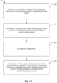
- FIG. 13 illustrates another flow diagram of a computer-implemented method that facilitates implementing a vertical Josephson junction superconducting device in accordance with one or more embodiments described herein.
- flow diagram 1300 can be implemented by operating environment 1400. It can be appreciated that the operations of flow diagram 1300 can be implemented in a different order than is depicted.
- a computing device (or system) (e.g., computer 1412) comprising one or more processors and one or more memories that stores executable instructions that, when executed by the one or more processors, can facilitate performance of the operations as described herein, including the non-limiting methods as illustrated in the flow diagrams of FIG. 13 .
- the one or more processors can facilitate performance of the methods by directing or controlling one or more equipment operable to perform semiconductor fabrication.
- An advantage of a method as depicted in FIG. 13 can be that it can be used to fabricate vertical Josephson junctions that are more uniform than Josephson junctions fabricated from previous techniques.
- Operation 1302 depicts bonding (e.g., by computer 1412) a first portion of a superconducting layer that is physically coupled to a crystalline silicon substrate with a second portion of the superconducting layer that is physically coupled with a second crystalline silicon substrate, the superconducting layer, and the second substrate comprising a SOM base.
- a first portion of the superconductor can be deposited on the first substrate, and a second portion of the superconductor can be deposited on the second substrate. Then, the first portion of the superconductor and the second portion of the superconductor can be bonded together, thus physically coupling the first substrate, the superconductor, and the second substrate.
- chip surface base device structure 100 where the substrate is substrate 106, the first superconducting layer is superconductor 104, and the second substrate is substrate 102.
- the substrate has a thickness of 100-200 nanometers (nm). This thickness of 100-200 nm can be obtained by growing crystalline silicon to that thickness, or by growing crystalline silicon to a thickness greater than 100-200 nm, and then - after physically coupling the substrate, the superconductor, and the second substrate - removing some of the crystalline silicon so that its thickness is then 100-200 nm.
- An advantage of using bonding to connect the substrate with the first superconducting layer, and the first superconducting layer with the second substrate can be to electrically isolate components of a chip surface base device structure, such as a vertical Josephson junction formed in the chip surface base device structure.
- Operation 1304 depicts forming (e.g., by computer 1412) a vertical Josephson junction in an etching of the crystalline silicon substrate, the vertical Josephson junction comprising the superconducting layer, a tunnel barrier layer, and a second superconducting layer.
- chip surface base device structure 900 An example of this arrangement of operation 1304 can be seen as chip surface base device structure 900 and as chip surface base device structure 1100.
- the vertical Josephson junction can be the combination of superconductor 408B, tunnel barrier 510B, and superconductor 910B.
- superconductor 408B can be considered to be an electrode of the vertical Josephson junction
- superconductor 910B can be considered to be another electrode of the vertical Josephson junction.
- the vertical Josephson junction can be the combination of superconductor 408B, tunnel barrier 510B, and superconductor 1010B. Then, superconductor 408B can be considered to be an electrode of the vertical Josephson junction, and superconductor 910B can be considered to be another electrode of the vertical Josephson junction.
- the etching of the substrate comprises a via.
- This via can be seen, for example, with chip surface base device structure 200, where the via can be the space between substrate 206A and substrate 206C.
- the tunnel barrier layer is deposited onto the first superconducting layer or a second superconducting layer.
- This former arrangement can be seen, for example, with chip surface base device structure 300, where the tunnel base layer can be tunnel barrier 308B, and it is deposited directly onto superconductor 104, which can be the first superconducting layer.
- the tunnel barrier layer being deposited on a second superconducting layer
- this latter arrangement can be seen, for example, with chip surface base device structure 500 where the tunnel base layer can be tunnel barrier 510B, and it is deposited on superconductor 408B, which can be the second superconducting layer.
- the vertical Josephson junction comprises a second superconducting layer that is deposited between the first superconducting layer and the tunnel barrier layer.
- This arrangement can be seen, for example, with chip surface base device structure 500, where the tunnel base layer can be tunnel barrier 510B, the first superconducting layer can be superconductor 104, and the second superconducting layer can be superconductor 408B.
- the first superconducting layer and the second superconducting layer each comprise an electrode of the vertical Josephson junction. This arrangement can be seen, for example, with chip surface base device structure 1100, where the first superconducting layer can be superconductor 408B, and the second superconducting layer can be superconductor 1010B.
- the tunnel barrier layer is deposited by sputtering, evaporating, or ALD.
- the second superconducting layer is deposited between the first superconducting layer and the tunnel barrier layer.
- This arrangement can be seen, for example, with chip surface base device structure 500, where the second superconducting layer can be superconductor 408B, the first superconducting layer can be superconductor 104, and the tunnel barrier layer can be tunnel barrier 510B.
- a height of the second superconducting layer is shorter than an initial height of the etching of the substrate.
- the initial height of the etching of the substrate is a height of what was etched from substrate 106 to form substrate 206A and substrate 206B
- the height of superconductor 712B is less than a height of what was etched from substrate 106 to form substrate 206A and substrate 206B.
- the second superconducting layer and the third superconducting layer are of a different type.
- the second superconducting layer can be superconductor 408B
- the third superconducting layer can be superconductor 712B (which each comprise an electrode of a vertical Josephson junction).
- superconductor 408B can be a first type of superconducting material
- superconductor 712B can be a second type of superconducting material.
- a CMP is used to remove a portion of the third superconducting layer.
- the third superconducting layer can be the combination of superconductor 610A, superconductor 610B, and superconductor 610C.
- a way in which chip surface base device structure 800 differs from chip surface base device structure 600 is that in chip surface base device structure 800 and relative to chip surface base device structure 600, superconductor 610A has been removed, a portion of superconductor 610B has been removed, and superconductor 610C has been removed.
- the vertical Josephson junction is formed within a via, and the via is formed using a mask and RIE.
- the vertical Josephson junction can comprise superconductor 408B, tunnel barrier 510B, and superconductor 1010B.
- This vertical Josephson junction is formed within a via, which can be a space created between substrate 206A and substrate 206B (where the space was created from substrate 106 in chip surface base device structure 100).
- This via can be formed using a mask and RIE.
- CMP is utilized remove a portion of the second superconducting layer that is located outside of the via.
- the second superconducting layer can be the combination of superconductor 408A and superconductor 408C (and can also include superconductor 910B).
- a portion of this second superconducting layer is removed (which is depicted as all of superconductor 408A, some of superconductor 910B, and all of superconductor 408C being removed to form chip surface base device structure 1000). Removing all of superconductor 408A, some of superconductor 910B, and all of superconductor 408C can be effectuated with CMP.
- a third superconducting layer is deposited on the substrate after removing the portion of the second superconducting layer that is located outside of the via.
- chip surface base device structure 1100 can include superconductor 1112 as the fourth superconducting layer, and the substrate can be substrate 206A and substrate 206B.
- Superconductor 1112 can be deposited on substrate 206A and substrate 206B, after superconductor 408A, part of superconductor 910B, and superconductor 408C (as depicted in chip surface base device structure 900) have been removed from chip surface base device structure 900 to produce chip surface base device structure 1000 (with chip surface base device structure 1100 being created from chip surface base device structure 1000 through depositing superconductor 1112).
- FIG. 14 as well as the following discussion are intended to provide a general description of a suitable environment in which the various aspects of the disclosed subject matter can be implemented.
- operating environment 1400 can be used to implement aspects of computer-implemented methods that facilitates implementing a vertical Josephson junction superconducting device of FIGS. 12 and 13 .
- FIG. 14 illustrates a block diagram of an operating environment in which examples or one or more embodiments described herein can be facilitated. Repetitive description of like elements employed in other embodiments described herein is omitted for sake of brevity.
- a suitable operating environment 1400 for implementing various aspects of this disclosure can also include a computer 1412.
- the computer 1412 can also include a processing unit 1414, a system memory 1416, and a system bus 1418.
- the system bus 1418 couples system components including, but not limited to, the system memory 1416 to the processing unit 1414.
- the processing unit 1414 can be any of various available processors. Dual microprocessors and other multiprocessor architectures also can be employed as the processing unit 1414.
- the system bus 1418 can be any of several types of bus structure(s) including the memory bus or memory controller, a peripheral bus or external bus, and/or a local bus using any variety of available bus architectures including, but not limited to, Industrial Standard Architecture (ISA), Micro-Channel Architecture (MSA), Extended ISA (EISA), Intelligent Drive Electronics (IDE), VESA Local Bus (VLB), Peripheral Component Interconnect (PCI), Card Bus, Universal Serial Bus (USB), Advanced Graphics Port (AGP), Firewire (IEEE 1394), and Small Computer Systems Interface (SCSI).
- ISA Industrial Standard Architecture
- MSA Micro-Channel Architecture
- EISA Extended ISA
- IDE Intelligent Drive Electronics
- VLB VESA Local Bus
- PCI Peripheral Component Interconnect
- Card Bus Universal Serial Bus
- USB Universal Serial Bus
- AGP Advanced Graphics Port
- Firewire IEEE 1394
- SCSI Small Computer Systems Interface
- the system memory 1416 can also include volatile memory 1420 and nonvolatile memory 1422.
- the basic input/output system (BIOS) containing the basic routines to transfer information between elements within the computer 1412, such as during start-up, is stored in nonvolatile memory 1422.
- nonvolatile memory 1422 can include read only memory (ROM), programmable ROM (PROM), electrically programmable ROM (EPROM), electrically erasable programmable ROM (EEPROM), flash memory, or nonvolatile random access memory (RAM) (e.g., ferroelectric RAM (FeRAM).
- Volatile memory 1420 can also include random access memory (RAM), which acts as external cache memory.
- RAM is available in many forms such as static RAM (SRAM), dynamic RAM (DRAM), synchronous DRAM (SDRAM), double data rate SDRAM (DDR SDRAM), enhanced SDRAM (ESDRAM), Synchlink DRAM (SLDRAM), direct Rambus RAM (DRRAM), direct Rambus dynamic RAM (DRDRAM), and Rambus dynamic RAM.
- SRAM static RAM
- DRAM dynamic RAM
- SDRAM synchronous DRAM
- DDR SDRAM double data rate SDRAM
- ESDRAM enhanced SDRAM
- SLDRAM Synchlink DRAM
- DRRAM direct Rambus RAM
- DRAM direct Rambus dynamic RAM
- Rambus dynamic RAM Rambus dynamic RAM
- Computer 1412 can also include removable/non-removable, volatile/non-volatile computer storage media.
- FIG. 14 illustrates, for example, a disk storage 1424.
- Disk storage 1424 can also include, but is not limited to, devices like a magnetic disk drive, floppy disk drive, tape drive, Jaz drive, Zip drive, LS-100 drive, flash memory card, or memory stick.
- the disk storage 1424 also can include storage media separately or in combination with other storage media including, but not limited to, an optical disk drive such as a compact disk ROM device (CD-ROM), CD recordable drive (CD-R Drive), CD rewritable drive (CD-RW Drive) or a digital versatile disk ROM drive (DVD-ROM).
- CD-ROM compact disk ROM device
- CD-R Drive CD recordable drive
- CD-RW Drive CD rewritable drive
- DVD-ROM digital versatile disk ROM drive
- FIG. 14 also depicts software that acts as an intermediary between users and the basic computer resources described in the suitable operating environment 1400.
- Such software can also include, for example, an operating system 1428.
- Operating system 1428 which can be stored on disk storage 1424, acts to control and allocate resources of the computer 1412.
- System applications 1430 take advantage of the management of resources by operating system 1428 through program modules 1432 and program data 1434, e.g., stored either in system memory 1416 or on disk storage 1424. It is to be appreciated that this disclosure can be implemented with various operating systems or combinations of operating systems.
- a user enters commands or information into the computer 1412 through input device(s) 1436.
- Input devices 1436 include, but are not limited to, a pointing device such as a mouse, trackball, stylus, touch pad, keyboard, microphone, joystick, game pad, satellite dish, scanner, TV tuner card, digital camera, digital video camera, web camera, and the like. These and other input devices connect to the processing unit 1414 through the system bus 1418 via interface port(s) 1438.
- Interface port(s) 1438 include, for example, a serial port, a parallel port, a game port, and a universal serial bus (USB).
- Output device(s) 1440 use some of the same type of ports as input device(s) 1436.
- a USB port can be used to provide input to computer 1412, and to output information from computer 1412 to an output device 1440.
- Output adapter 1442 is provided to illustrate that there are some output devices 1440 like monitors, speakers, and printers, among other output devices 1440, which require special adapters.
- the output adapters 1442 include, by way of illustration and not limitation, video and sound cards that provide a means of connection between the output device 1440 and the system bus 1418. It should be noted that other devices and/or systems of devices provide both input and output capabilities such as remote computer(s) 1444.
- Computer 1412 can operate in a networked environment using logical connections to one or more remote computers, such as remote computer(s) 1444.
- the remote computer(s) 1444 can be a computer, a server, a router, a network PC, a workstation, a microprocessor based appliance, a peer device or other common network node and the like, and typically can also include many or all of the elements described relative to computer 1412. For purposes of brevity, only a memory storage device 1446 is illustrated with remote computer(s) 1444.
- Remote computer(s) 1444 is logically connected to computer 1412 through a network interface 1448 and then physically connected via communication connection 1450.
- Network interface 1448 encompasses wire and/or wireless communication networks such as local-area networks (LAN), wide-area networks (WAN), cellular networks, etc.
- LAN technologies include Fiber Distributed Data Interface (FDDI), Copper Distributed Data Interface (CDDI), Ethernet, Token Ring and the like.
- WAN technologies include, but are not limited to, point-to-point links, circuit switching networks like Integrated Services Digital Networks (ISDN) and variations thereon, packet switching networks, and Digital Subscriber Lines (DSL).
- Communication connection(s) 1450 refers to the hardware/software employed to connect the network interface 1448 to the system bus 1418. While communication connection 1450 is shown for illustrative clarity inside computer 1412, it can also be external to computer 1412.
- the hardware/software for connection to the network interface 1448 can also include, for exemplary purposes only, internal and external technologies such as, modems including regular telephone grade modems, cable modems and DSL modems, ISDN adapters, and Ethernet cards.
- the present invention can be implemented at any possible technical detail level of integration.
- the computer program product can include a computer readable storage medium (or media) having computer readable program instructions thereon for causing a processor to carry out aspects of the present invention.
- the computer readable storage medium can be a tangible device that can retain and store instructions for use by an instruction execution device.
- the computer readable storage medium can be, for example, but is not limited to, an electronic storage device, a magnetic storage device, an optical storage device, an electromagnetic storage device, a semiconductor storage device, or any suitable combination of the foregoing.
- a non-exhaustive list of more specific examples of the computer readable storage medium can also include the following: a portable computer diskette, a hard disk, a random access memory (RAM), a read-only memory (ROM), an erasable programmable read-only memory (EPROM or Flash memory), a static random access memory (SRAM), a portable compact disc read-only memory (CD-ROM), a digital versatile disk (DVD), a memory stick, a floppy disk, a mechanically encoded device such as punch-cards or raised structures in a groove having instructions recorded thereon, and any suitable combination of the foregoing.
- RAM random access memory
- ROM read-only memory
- EPROM or Flash memory erasable programmable read-only memory
- SRAM static random access memory
- CD-ROM compact disc read-only memory
- DVD digital versatile disk
- memory stick a floppy disk
- a mechanically encoded device such as punch-cards or raised structures in a groove having instructions recorded thereon
- a computer readable storage medium is not to be construed as being transitory signals per se, such as radio waves or other freely propagating electromagnetic waves, electromagnetic waves propagating through a waveguide or other transmission media (e.g., light pulses passing through a fiber-optic cable), or electrical signals transmitted through a wire.
- Computer readable program instructions described herein can be downloaded to respective computing/processing devices from a computer readable storage medium or to an external computer or external storage device via a network, for example, the Internet, a local area network, a wide area network and/or a wireless network.
- the network can comprise copper transmission cables, optical transmission fibers, wireless transmission, routers, firewalls, switches, gateway computers and/or edge servers.
- a network adapter card or network interface in each computing/processing device receives computer readable program instructions from the network and forwards the computer readable program instructions for storage in a computer readable storage medium within the respective computing/processing device.
- Computer readable program instructions for carrying out operations of the present invention can be assembler instructions, instruction-set-architecture (ISA) instructions, machine instructions, machine dependent instructions, microcode, firmware instructions, state-setting data, configuration data for integrated circuitry, or either source code or object code written in any combination of one or more programming languages, including an object oriented programming language such as Smalltalk, C++, or the like, and procedural programming languages, such as the "C" programming language or similar programming languages.
- the computer readable program instructions can execute entirely on the user's computer, partly on the user's computer, as a stand-alone software package, partly on the user's computer and partly on a remote computer or entirely on the remote computer or server.
- the remote computer can be connected to the user's computer through any type of network, including a local area network (LAN) or a wide area network (WAN), or the connection can be made to an external computer (for example, through the Internet using an Internet Service Provider).
- electronic circuitry including, for example, programmable logic circuitry, field-programmable gate arrays (FPGA), or programmable logic arrays (PLA) can execute the computer readable program instructions by utilizing state information of the computer readable program instructions to personalize the electronic circuitry, in order to perform aspects of the present invention.
- These computer readable program instructions can also be stored in a computer readable storage medium that can direct a computer, a programmable data processing apparatus, and/or other devices to function in a particular manner, such that the computer readable storage medium having instructions stored therein comprises an article of manufacture including instructions which implement aspects of the function/act specified in the flowchart and/or block diagram block or blocks.
- the computer readable program instructions can also be loaded onto a computer, other programmable data processing apparatus, or other device to cause a series of operational acts to be performed on the computer, other programmable apparatus or other device to produce a computer-implemented process, such that the instructions which execute on the computer, other programmable apparatus, or other device implement the functions/acts specified in the flowchart and/or block diagram block or blocks.
- each block in the flowchart or block diagrams can represent a module, segment, or portion of instructions, which comprises one or more executable instructions for implementing the specified logical function(s).
- the functions noted in the blocks can occur out of the order noted in the Figures.
- two blocks shown in succession can, in fact, be executed substantially concurrently, or the blocks can sometimes be executed in the reverse order, depending upon the functionality involved.
- program modules include routines, programs, components, data structures, etc. that perform particular tasks and/or implement particular abstract data types.
- inventive computer-implemented methods can be practiced with other computer system configurations, including single-processor or multiprocessor computer systems, mini-computing devices, mainframe computers, as well as computers, hand-held computing devices (e.g., PDA, phone), microprocessor-based or programmable consumer or industrial electronics, and the like.
- the illustrated aspects can also be practiced in distributed computing environments in which tasks are performed by remote processing devices that are linked through a communications network. However, some, if not all aspects of this disclosure can be practiced on stand-alone computers. In a distributed computing environment, program modules can be located in both local and remote memory storage devices.
- ком ⁇ онент can refer to and/or can include a computer-related entity or an entity related to an operational machine with one or more specific functionalities.
- the entities disclosed herein can be either hardware, a combination of hardware and software, software, or software in execution.
- a component can be, but is not limited to being, a process running on a processor, a processor, an object, an executable, a thread of execution, a program, and/or a computer.
- an application running on a server and the server can be a component.
- One or more components can reside within a process and/or thread of execution and a component can be localized on one computer and/or distributed between two or more computers.
- respective components can execute from various computer readable media having various data structures stored thereon.
- the components can communicate via local and/or remote processes such as in accordance with a signal having one or more data packets (e.g., data from one component interacting with another component in a local system, distributed system, and/or across a network such as the Internet with other systems via the signal).
- a component can be an apparatus with specific functionality provided by mechanical parts operated by electric or electronic circuitry, which is operated by a software or firmware application executed by a processor.
- a component can be an apparatus that provides specific functionality through electronic components without mechanical parts, wherein the electronic components can include a processor or other means to execute software or firmware that confers at least in part the functionality of the electronic components.
- a component can emulate an electronic component via a virtual machine, e.g., within a cloud computing system.
- processor can refer to substantially any computing processing unit or device comprising, but not limited to, single-core processors; single-processors with software multithread execution capability; multi-core processors; multi-core processors with software multithread execution capability; multi-core processors with hardware multithread technology; parallel platforms; and parallel platforms with distributed shared memory.
- a processor can refer to an integrated circuit, an application specific integrated circuit (ASIC), a digital signal processor (DSP), a field programmable gate array (FPGA), a programmable logic controller (PLC), a complex programmable logic device (CPLD), a discrete gate or transistor logic, discrete hardware components, or any combination thereof designed to perform the functions described herein.
- ASIC application specific integrated circuit
- DSP digital signal processor
- FPGA field programmable gate array
- PLC programmable logic controller
- CPLD complex programmable logic device
- processors can exploit nano-scale architectures such as, but not limited to, molecular and quantum-dot based transistors, switches and gates, in order to optimize space usage or enhance performance of user equipment.
- a processor can also be implemented as a combination of computing processing units.
- terms such as “store,” “storage,” “data store,” data storage,” “database,” and substantially any other information storage component relevant to operation and functionality of a component are utilized to refer to "memory components," entities embodied in a "memory,” or components comprising a memory. It is to be appreciated that memory and/or memory components described herein can be either volatile memory or nonvolatile memory, or can include both volatile and nonvolatile memory.
- nonvolatile memory can include read only memory (ROM), programmable ROM (PROM), electrically programmable ROM (EPROM), electrically erasable ROM (EEPROM), flash memory, or nonvolatile random access memory (RAM) (e.g., ferroelectric RAM (FeRAM).
- Volatile memory can include RAM, which can act as external cache memory, for example.
- RAM is available in many forms such as synchronous RAM (SRAM), dynamic RAM (DRAM), synchronous DRAM (SDRAM), double data rate SDRAM (DDR SDRAM), enhanced SDRAM (ESDRAM), Synchlink DRAM (SLDRAM), direct Rambus RAM (DRRAM), direct Rambus dynamic RAM (DRDRAM), and Rambus dynamic RAM (RDRAM).
- SRAM synchronous RAM
- DRAM dynamic RAM
- SDRAM synchronous DRAM
- DDR SDRAM double data rate SDRAM
- ESDRAM enhanced SDRAM
- SLDRAM Synchlink DRAM
- DRRAM direct Rambus RAM
- DRAM direct Rambus dynamic RAM
- RDRAM Rambus dynamic RAM
Landscapes
- Engineering & Computer Science (AREA)
- Physics & Mathematics (AREA)
- Mathematical Physics (AREA)
- Chemical & Material Sciences (AREA)
- Nanotechnology (AREA)
- Computer Hardware Design (AREA)
- Computing Systems (AREA)
- General Engineering & Computer Science (AREA)
- Theoretical Computer Science (AREA)
- Crystallography & Structural Chemistry (AREA)
- Manufacturing & Machinery (AREA)
- Superconductor Devices And Manufacturing Methods Thereof (AREA)
Claims (16)
- Chipoberflächenstruktur einer Basisvorrichtung (100, 200, 300, 400, 500, 600, 700, 800, 900, 1000, 1100), umfassend:ein erstes Substrat (106), das kristallines Silizium umfasst, das physikalisch mit einer ersten supraleitenden Schicht (104) gekoppelt ist, wobei die erste supraleitende Schicht (104) physikalisch mit einem zweiten kristallinen Siliziumsubstrat (102) gekoppelt ist, wobei das erste Substrat (106), die supraleitende Schicht (104) und das zweite kristalline Siliziumsubstrat eine Silizium-auf-Metall-, SOM-, Basis umfassen; undeinen vertikalen Josephson-Übergang (1114), der sich in einem geätzten Bereich des ersten Substrats (106) befindet, wobei der vertikale Josephson-Übergang (1114) die erste supraleitende Schicht (104), eine Tunnelbarriereschicht (510B) und eine obere supraleitende Schicht (1010B) umfasst.
- Chipoberflächenstruktur einer Basisvorrichtung nach Anspruch 1, weiter umfassend:
eine Durchkontaktierung (208) in dem geätzten Bereich des ersten Substrats (106). - Chipoberflächenstruktur einer Basisvorrichtung nach Anspruch 1, wobei sich die Tunnelbarriereschicht (510B) auf mindestens einer von der ersten supraleitenden Schicht (104) oder einer zweiten supraleitenden Schicht (408B), die physikalisch mit der ersten supraleitenden Schicht (104) gekoppelt ist, befindet.
- Chipoberflächenstruktur einer Basisvorrichtung nach Anspruch 1, wobei der vertikale Josephson-Übergang (1114) eine dritte supraleitende Schicht (610B, 712B) umfasst, die über der Tunnelbarriereschicht (510B) abgelagert ist.
- Chipoberflächenstruktur einer Basisvorrichtung nach Anspruch 1, wobei die erste supraleitende Schicht (104) eine erste Elektrode (1120) des vertikalen Josephson-Übergangs (1114) umfasst und die obere supraleitende Schicht (1010B), die sich auf einer der ersten supraleitenden Schicht (104) gegenüberliegenden Seite (1116) der Tunnelbarriereschicht (510B) befindet, eine obere Elektrode (1118) des vertikalen Josephson-Übergangs (1114) umfasst.
- Chipoberflächenstruktur einer Basisvorrichtung nach Anspruch 1, wobei der vertikale Josephson-Übergang (1114) eine erste Elektrode (1120), die die erste supraleitende Schicht (104) oder eine zweite supraleitende Schicht (408A) umfasst, und eine zweite Elektrode (1118), die die obere supraleitende Schicht (1010B) umfasst, umfasst.
- Chipoberflächenstruktur einer Basisvorrichtung nach Anspruch 1, wobei sich die erste supraleitende Schicht (104) zwischen dem ersten Substrat (106) und dem zweiten Substrat (102) befindet und diese verbindet.
- Chipoberflächenstruktur einer Basisvorrichtung nach Anspruch 1, wobei eine dritte supraleitende Schicht (610B, 712B) über der ersten supraleitenden Schicht (104) und der Tunnelbarriereschicht (510B) oder über einer zweiten supraleitenden Schicht (408B) und der Tunnelbarriereschicht (510B) abgelagert ist.
- Verfahren, umfassend:physikalisches Koppeln eines ersten Substrats (106), das kristallines Silizium umfasst, mit einer ersten supraleitenden Schicht (104);physikalisches Koppeln der ersten supraleitenden Schicht (104) mit einem zweiten kristallinen Siliziumsubstrat (102), wobei das erste Substrat (106), die supraleitende Schicht (104) und das zweite kristalline Siliziumsubstrat eine Silizium-auf-Metall-, SOM-, Basis umfassen;Ätzen des ersten Substrats (106); undBilden eines vertikalen Josephson-Übergangs (1114) in einem geätzten Bereich des ersten Substrats (106), wobei der vertikale Josephson-Übergang (1114) die erste supraleitende Schicht (104), eine Tunnelbarriereschicht (510B) und eine obere supraleitende Schicht (1010B) umfasst.
- Verfahren nach Anspruch 9, weiter umfassend:
Ablagern der Tunnelbarriereschicht (510B) durch Durchführen des Prozesses innerhalb einer Gruppe bestehend aus Sputtern, Verdampfen, Atomlagenablagerung, Wachsen, chemischer Modifikation und Oxidation. - Verfahren nach Anspruch 9, weiter umfassend:
Ablagern einer zweiten supraleitenden Schicht (408B) zwischen der ersten supraleitenden Schicht (104) und der Tunnelbarriereschicht (510B). - Verfahren nach Anspruch 11, wobei eine Höhe der zweiten supraleitenden Schicht (408B) kürzer ist als eine zweite Höhe der Ätzung des ersten Substrats (106), wobei die zweite Höhe eine Anfangshöhe der Ätzung des ersten Substrats (106) beim Bilden der Ätzung umfasst.
- Verfahren nach Anspruch 12, weiter umfassend:
Ablagern einer dritten supraleitenden Schicht (610B, 712B) auf der Tunnelbarriereschicht (510B). - Verfahren nach Anspruch 13, wobei die zweite supraleitende Schicht (408B) und die dritte supraleitende Schicht (610B, 712B) von unterschiedlichem Typ sind.
- Verfahren nach Anspruch 13, weiter umfassend:
Durchführen einer chemisch-mechanischen Planarisierung, um einen Abschnitt der dritten supraleitenden Schicht (610B, 712B) zu entfernen. - Verfahren nach Anspruch 9, weiter umfassend:Bilden einer Durchkontaktierung (208) unter Einsatz einer Maske und eines reaktiven lonenätzens; undBilden des vertikalen Josephson-Übergangs (1114) innerhalb der Durchkontaktierung (208).
Applications Claiming Priority (2)
| Application Number | Priority Date | Filing Date | Title |
|---|---|---|---|
| US15/934,400 US10243132B1 (en) | 2018-03-23 | 2018-03-23 | Vertical josephson junction superconducting device |
| PCT/EP2019/054837 WO2019179732A1 (en) | 2018-03-23 | 2019-02-27 | Vertical josephson junction superconducting device |
Publications (3)
| Publication Number | Publication Date |
|---|---|
| EP3769347A1 EP3769347A1 (de) | 2021-01-27 |
| EP3769347C0 EP3769347C0 (de) | 2024-09-11 |
| EP3769347B1 true EP3769347B1 (de) | 2024-09-11 |
Family
ID=65657450
Family Applications (1)
| Application Number | Title | Priority Date | Filing Date |
|---|---|---|---|
| EP19708811.5A Active EP3769347B1 (de) | 2018-03-23 | 2019-02-27 | Vertikale josephson-kontaktvorrichtung |
Country Status (5)
| Country | Link |
|---|---|
| US (2) | US10243132B1 (de) |
| EP (1) | EP3769347B1 (de) |
| JP (1) | JP7362195B2 (de) |
| CN (1) | CN111937168B (de) |
| WO (1) | WO2019179732A1 (de) |
Families Citing this family (27)
| Publication number | Priority date | Publication date | Assignee | Title |
|---|---|---|---|---|
| US8536566B2 (en) | 2008-09-03 | 2013-09-17 | D-Wave Systems Inc. | Systems, methods and apparatus for active compensation of quantum processor elements |
| US9768371B2 (en) | 2012-03-08 | 2017-09-19 | D-Wave Systems Inc. | Systems and methods for fabrication of superconducting integrated circuits |
| US11038095B2 (en) | 2017-02-01 | 2021-06-15 | D-Wave Systems Inc. | Systems and methods for fabrication of superconducting integrated circuits |
| US10672971B2 (en) * | 2018-03-23 | 2020-06-02 | International Business Machines Corporation | Vertical transmon qubit device with microstrip waveguides |
| US10256392B1 (en) | 2018-03-23 | 2019-04-09 | International Business Machines Corporation | Vertical transmon qubit device |
| US10243132B1 (en) * | 2018-03-23 | 2019-03-26 | International Business Machines Corporation | Vertical josephson junction superconducting device |
| US20200152851A1 (en) | 2018-11-13 | 2020-05-14 | D-Wave Systems Inc. | Systems and methods for fabricating superconducting integrated circuits |
| US10720563B1 (en) | 2018-11-13 | 2020-07-21 | Google Llc | Quantum processor design to increase control footprint |
| US12102017B2 (en) | 2019-02-15 | 2024-09-24 | D-Wave Systems Inc. | Kinetic inductance for couplers and compact qubits |
| US11088310B2 (en) * | 2019-04-29 | 2021-08-10 | International Business Machines Corporation | Through-silicon-via fabrication in planar quantum devices |
| CN112054113B (zh) * | 2019-06-06 | 2024-03-22 | 阿里巴巴集团控股有限公司 | 超导电路及其制备方法 |
| US11600760B2 (en) * | 2019-11-26 | 2023-03-07 | Northrop Grumman Systems Corporation | Cooler device with aluminum oxide insulators |
| EP4070392B1 (de) | 2019-12-05 | 2026-02-04 | D-Wave Systems Inc. | Systeme und verfahren zur herstellung von supraleitenden integrierten schaltungen |
| US11309479B2 (en) | 2019-12-06 | 2022-04-19 | International Business Machines Corporation | Computing devices containing magnetic Josephson Junctions with embedded magnetic field control element |
| US20210280763A1 (en) * | 2019-12-23 | 2021-09-09 | Microsoft Technology Licensing, Llc | Superconductor heterostructures for semiconductor-superconductor hybrid structures |
| CN111244259B (zh) * | 2020-01-20 | 2023-07-25 | 中国科学院上海微系统与信息技术研究所 | 一种约瑟夫森结及超导量子干涉器件的制备方法 |
| CN113257988B (zh) | 2020-04-01 | 2022-05-06 | 阿里巴巴集团控股有限公司 | 硬掩模及其制备方法、约瑟夫森结的制备方法及超导电路 |
| WO2021231224A1 (en) | 2020-05-11 | 2021-11-18 | D-Wave Systems Inc. | Kinetic inductance devices, methods for fabricating kinetic inductance devices, and articles employing the same |
| JP7705897B2 (ja) * | 2020-06-23 | 2025-07-10 | ディー-ウェイブ システムズ インコーポレイテッド | 超伝導集積回路を製造する方法 |
| EP4009387B1 (de) * | 2020-12-07 | 2023-06-07 | IQM Finland Oy | Verfahren zur herstellung eines josephson-übergangs |
| WO2022261523A1 (en) | 2021-06-11 | 2022-12-15 | SeeQC, Inc. | System and method of flux bias for superconducting quantum circuits |
| US20240260486A1 (en) * | 2021-07-20 | 2024-08-01 | 1372934 B.C. Ltd. | Systems and methods for quantum computing using fluxonium qubits with kinetic inductors |
| CN113848001B (zh) * | 2021-09-14 | 2023-12-15 | 东南大学 | 一种rf谐振压力传感器 |
| US12392823B2 (en) | 2021-11-05 | 2025-08-19 | D-Wave Systems Inc. | Systems and methods for on-chip noise measurements |
| KR20240001112A (ko) * | 2022-06-23 | 2024-01-03 | 텐센트 테크놀로지(센젠) 컴퍼니 리미티드 | 조셉슨 접합을 마련하기 위한 방법 및 시스템 |
| CN115666212B (zh) * | 2022-12-12 | 2023-06-02 | 量子科技长三角产业创新中心 | 一种超导量子约瑟夫森结的制备方法及相关装置 |
| US20250040452A1 (en) * | 2023-07-25 | 2025-01-30 | Northrop Grumman Systems Corporation | Continuous long josephson junction logic gate system |
Family Cites Families (38)
| Publication number | Priority date | Publication date | Assignee | Title |
|---|---|---|---|---|
| EP0325877B1 (de) | 1987-12-26 | 1994-03-09 | Sumitomo Electric Industries Limited | Halbleitersubstrat mit einem supraleitenden Dünnfilm |
| US5523282A (en) | 1988-08-18 | 1996-06-04 | Trw Inc. | High-frequency substrate material for thin-film layered perovskite superconductors |
| US5157466A (en) | 1991-03-19 | 1992-10-20 | Conductus, Inc. | Grain boundary junctions in high temperature superconductor films |
| US5385883A (en) | 1993-05-17 | 1995-01-31 | The United States Of America As Represented By The Secretary Of The Army | High Tc superconducting microstrip phase shifter having tapered optical beam pattern regions |
| US5476719A (en) | 1994-08-17 | 1995-12-19 | Trw Inc. | Superconducting multi-layer microstrip structure for multi-chip modules and microwave circuits |
| EP0823734A1 (de) | 1996-07-23 | 1998-02-11 | DORNIER GmbH | Josephson-Übergangs-Array-Anordnung und Verfahren zu ihrer Herstellung |
| JP4172936B2 (ja) | 2000-01-28 | 2008-10-29 | 富士通株式会社 | 超伝導マイクロストリップフィルタ |
| KR100368930B1 (ko) | 2001-03-29 | 2003-01-24 | 한국과학기술원 | 반도체 기판 위에 높이 떠 있는 3차원 금속 소자, 그 회로모델, 및 그 제조방법 |
| US6734454B2 (en) | 2001-08-27 | 2004-05-11 | The Regents Of The University Of California | Internally shunted Josephson junction device |
| US6979836B2 (en) | 2001-08-29 | 2005-12-27 | D-Wave Systems, Inc. | Superconducting low inductance qubit |
| AU2002950888A0 (en) | 2002-08-20 | 2002-09-12 | Unisearch Limited | Quantum device |
| US6818549B2 (en) | 2003-03-05 | 2004-11-16 | Hewlett-Packard Development Company, L.P. | Buried magnetic tunnel-junction memory cell and methods |
| US6926921B2 (en) | 2003-05-05 | 2005-08-09 | Hewlett-Packard Development Company, L.P. | Imprint lithography for superconductor devices |
| US20080032501A1 (en) | 2006-07-21 | 2008-02-07 | Honeywell International Inc. | Silicon on metal for mems devices |
| US7615385B2 (en) | 2006-09-20 | 2009-11-10 | Hypres, Inc | Double-masking technique for increasing fabrication yield in superconducting electronics |
| US7888746B2 (en) | 2006-12-15 | 2011-02-15 | Hvvi Semiconductors, Inc. | Semiconductor structure and method of manufacture |
| US9768371B2 (en) | 2012-03-08 | 2017-09-19 | D-Wave Systems Inc. | Systems and methods for fabrication of superconducting integrated circuits |
| US20160104073A1 (en) | 2012-12-05 | 2016-04-14 | The United States Of America As Represented By The Secretary Of Commerce | Radiation Suppression of Superconducting Quantum Bits Using a Conductive Plane |
| CA2898598C (en) | 2013-01-18 | 2023-01-03 | Yale University | Superconducting device with at least one enclosure |
| CA2898608C (en) | 2013-01-18 | 2022-01-11 | Yale University | Methods for making a superconducting device with at least one enclosure |
| US9520547B2 (en) | 2013-03-15 | 2016-12-13 | International Business Machines Corporation | Chip mode isolation and cross-talk reduction through buried metal layers and through-vias |
| US9425377B2 (en) | 2013-04-19 | 2016-08-23 | The Regents Of The University Of California | Tunnel junction fabrication |
| US9741918B2 (en) | 2013-10-07 | 2017-08-22 | Hypres, Inc. | Method for increasing the integration level of superconducting electronics circuits, and a resulting circuit |
| US9324767B1 (en) | 2013-12-31 | 2016-04-26 | Intermolecular, Inc. | Superconducting junctions |
| CN106575667B (zh) | 2014-07-02 | 2020-07-31 | 哥本哈根大学 | 半导体约瑟夫森结及其相关的传输子量子位 |
| US9501748B2 (en) | 2014-11-04 | 2016-11-22 | Northrop Grumman Systems Corporation | Mixed coupling between a qubit and resonator |
| US9929334B2 (en) * | 2015-01-15 | 2018-03-27 | International Business Machines Corporation | Josephson junction with spacer |
| US9455391B1 (en) * | 2015-05-19 | 2016-09-27 | The United States Of America As Represented By Secretary Of The Navy | Advanced process flow for quantum memory devices and josephson junctions with heterogeneous integration |
| US10074793B2 (en) * | 2015-06-29 | 2018-09-11 | International Business Machines Corporation | Incorporating arrays of Josephson junctions in a Josephson junction ring modulator in a Josephson parametric converter |
| EP3130031B1 (de) | 2015-07-06 | 2019-12-04 | Rigetti & Co., Inc. | Vorrichtung mit konzentriertem element für quanteninformationsverarbeitungssysteme |
| WO2017015432A1 (en) | 2015-07-23 | 2017-01-26 | Massachusetts Institute Of Technology | Superconducting integrated circuit |
| WO2017131831A2 (en) | 2015-11-05 | 2017-08-03 | Massachusetts Institute Of Technology | Qubit and coupler circuit structures and coupling techniques |
| US20170186935A1 (en) | 2015-12-29 | 2017-06-29 | Intermolecular, Inc. | Low Temperature Deposition of Silicon Containing Layers in Superconducting Circuits |
| WO2017217961A1 (en) | 2016-06-13 | 2017-12-21 | Intel Corporation | Josephson junctions made from refractory and noble metals |
| US10608159B2 (en) | 2016-11-15 | 2020-03-31 | Northrop Grumman Systems Corporation | Method of making a superconductor device |
| US10255557B2 (en) * | 2017-02-15 | 2019-04-09 | Northrop Grumman Systems Corporation | XX Coupler for flux qubits |
| US10243132B1 (en) * | 2018-03-23 | 2019-03-26 | International Business Machines Corporation | Vertical josephson junction superconducting device |
| US10256392B1 (en) | 2018-03-23 | 2019-04-09 | International Business Machines Corporation | Vertical transmon qubit device |
-
2018
- 2018-03-23 US US15/934,400 patent/US10243132B1/en active Active
-
2019
- 2019-01-14 US US16/246,676 patent/US10784432B2/en active Active
- 2019-02-27 WO PCT/EP2019/054837 patent/WO2019179732A1/en not_active Ceased
- 2019-02-27 EP EP19708811.5A patent/EP3769347B1/de active Active
- 2019-02-27 CN CN201980021512.7A patent/CN111937168B/zh active Active
- 2019-02-27 JP JP2020549012A patent/JP7362195B2/ja active Active
Also Published As
| Publication number | Publication date |
|---|---|
| US10784432B2 (en) | 2020-09-22 |
| JP7362195B2 (ja) | 2023-10-17 |
| US20190296212A1 (en) | 2019-09-26 |
| CN111937168B (zh) | 2024-09-03 |
| JP2021518655A (ja) | 2021-08-02 |
| CN111937168A (zh) | 2020-11-13 |
| EP3769347C0 (de) | 2024-09-11 |
| WO2019179732A1 (en) | 2019-09-26 |
| US10243132B1 (en) | 2019-03-26 |
| EP3769347A1 (de) | 2021-01-27 |
Similar Documents
| Publication | Publication Date | Title |
|---|---|---|
| EP3769347B1 (de) | Vertikale josephson-kontaktvorrichtung | |
| US10714672B2 (en) | Vertical transmon qubit device | |
| EP3769341B1 (de) | Vertikale transmon qubit vorrichtung mit mikrostreifen-wellenleitern | |
| EP3807935B1 (de) | Vertikales silicium-auf-metall supraleitendes quanteninterferenzelement und herstellungsverfahren | |
| US11605772B2 (en) | Vertical dispersive readout of qubits of a lattice surface code architecture | |
| US10840296B2 (en) | Three-dimensional integration for qubits on crystalline dielectric | |
| US11581474B2 (en) | Electrical leads for trenched qubits | |
| US12096702B2 (en) | Epitaxial Josephson junction device | |
| US11380836B2 (en) | Topological qubit device | |
| EP4022684B1 (de) | Ionenimplantatdefinierter nanostab in einer suspendierten majorana-fermionen-vorrichtung |
Legal Events
| Date | Code | Title | Description |
|---|---|---|---|
| STAA | Information on the status of an ep patent application or granted ep patent |
Free format text: STATUS: UNKNOWN |
|
| STAA | Information on the status of an ep patent application or granted ep patent |
Free format text: STATUS: THE INTERNATIONAL PUBLICATION HAS BEEN MADE |
|
| PUAI | Public reference made under article 153(3) epc to a published international application that has entered the european phase |
Free format text: ORIGINAL CODE: 0009012 |
|
| STAA | Information on the status of an ep patent application or granted ep patent |
Free format text: STATUS: REQUEST FOR EXAMINATION WAS MADE |
|
| 17P | Request for examination filed |
Effective date: 20201015 |
|
| AK | Designated contracting states |
Kind code of ref document: A1 Designated state(s): AL AT BE BG CH CY CZ DE DK EE ES FI FR GB GR HR HU IE IS IT LI LT LU LV MC MK MT NL NO PL PT RO RS SE SI SK SM TR |
|
| AX | Request for extension of the european patent |
Extension state: BA ME |
|
| DAV | Request for validation of the european patent (deleted) | ||
| DAX | Request for extension of the european patent (deleted) | ||
| STAA | Information on the status of an ep patent application or granted ep patent |
Free format text: STATUS: EXAMINATION IS IN PROGRESS |
|
| 17Q | First examination report despatched |
Effective date: 20210811 |
|
| REG | Reference to a national code |
Ref country code: DE Ref legal event code: R079 Free format text: PREVIOUS MAIN CLASS: H01L0039220000 Ref country code: DE Ref legal event code: R079 Ref document number: 602019058652 Country of ref document: DE Free format text: PREVIOUS MAIN CLASS: H01L0039220000 Ipc: H10N0060010000 |
|
| RIC1 | Information provided on ipc code assigned before grant |
Ipc: H03K 19/195 20060101ALI20240419BHEP Ipc: G06N 10/00 20190101ALI20240419BHEP Ipc: B82Y 40/00 20110101ALI20240419BHEP Ipc: B82Y 10/00 20110101ALI20240419BHEP Ipc: H10N 60/12 20230101ALI20240419BHEP Ipc: H10N 60/01 20230101AFI20240419BHEP |
|
| GRAP | Despatch of communication of intention to grant a patent |
Free format text: ORIGINAL CODE: EPIDOSNIGR1 |
|
| STAA | Information on the status of an ep patent application or granted ep patent |
Free format text: STATUS: GRANT OF PATENT IS INTENDED |
|
| INTG | Intention to grant announced |
Effective date: 20240613 |
|
| GRAS | Grant fee paid |
Free format text: ORIGINAL CODE: EPIDOSNIGR3 |
|
| GRAA | (expected) grant |
Free format text: ORIGINAL CODE: 0009210 |
|
| STAA | Information on the status of an ep patent application or granted ep patent |
Free format text: STATUS: THE PATENT HAS BEEN GRANTED |
|
| AK | Designated contracting states |
Kind code of ref document: B1 Designated state(s): AL AT BE BG CH CY CZ DE DK EE ES FI FR GB GR HR HU IE IS IT LI LT LU LV MC MK MT NL NO PL PT RO RS SE SI SK SM TR |
|
| REG | Reference to a national code |
Ref country code: GB Ref legal event code: FG4D |
|
| REG | Reference to a national code |
Ref country code: CH Ref legal event code: EP |
|
| REG | Reference to a national code |
Ref country code: DE Ref legal event code: R096 Ref document number: 602019058652 Country of ref document: DE |
|
| REG | Reference to a national code |
Ref country code: IE Ref legal event code: FG4D |
|
| U01 | Request for unitary effect filed |
Effective date: 20240917 |
|
| U07 | Unitary effect registered |
Designated state(s): AT BE BG DE DK EE FI FR IT LT LU LV MT NL PT RO SE SI Effective date: 20240924 |
|
| PG25 | Lapsed in a contracting state [announced via postgrant information from national office to epo] |
Ref country code: NO Free format text: LAPSE BECAUSE OF FAILURE TO SUBMIT A TRANSLATION OF THE DESCRIPTION OR TO PAY THE FEE WITHIN THE PRESCRIBED TIME-LIMIT Effective date: 20241211 |
|
| PG25 | Lapsed in a contracting state [announced via postgrant information from national office to epo] |
Ref country code: GR Free format text: LAPSE BECAUSE OF FAILURE TO SUBMIT A TRANSLATION OF THE DESCRIPTION OR TO PAY THE FEE WITHIN THE PRESCRIBED TIME-LIMIT Effective date: 20241212 |
|
| PG25 | Lapsed in a contracting state [announced via postgrant information from national office to epo] |
Ref country code: HR Free format text: LAPSE BECAUSE OF FAILURE TO SUBMIT A TRANSLATION OF THE DESCRIPTION OR TO PAY THE FEE WITHIN THE PRESCRIBED TIME-LIMIT Effective date: 20240911 |
|
| PG25 | Lapsed in a contracting state [announced via postgrant information from national office to epo] |
Ref country code: RS Free format text: LAPSE BECAUSE OF FAILURE TO SUBMIT A TRANSLATION OF THE DESCRIPTION OR TO PAY THE FEE WITHIN THE PRESCRIBED TIME-LIMIT Effective date: 20241211 Ref country code: ES Free format text: LAPSE BECAUSE OF FAILURE TO SUBMIT A TRANSLATION OF THE DESCRIPTION OR TO PAY THE FEE WITHIN THE PRESCRIBED TIME-LIMIT Effective date: 20240911 |
|
| PG25 | Lapsed in a contracting state [announced via postgrant information from national office to epo] |
Ref country code: RS Free format text: LAPSE BECAUSE OF FAILURE TO SUBMIT A TRANSLATION OF THE DESCRIPTION OR TO PAY THE FEE WITHIN THE PRESCRIBED TIME-LIMIT Effective date: 20241211 Ref country code: NO Free format text: LAPSE BECAUSE OF FAILURE TO SUBMIT A TRANSLATION OF THE DESCRIPTION OR TO PAY THE FEE WITHIN THE PRESCRIBED TIME-LIMIT Effective date: 20241211 Ref country code: HR Free format text: LAPSE BECAUSE OF FAILURE TO SUBMIT A TRANSLATION OF THE DESCRIPTION OR TO PAY THE FEE WITHIN THE PRESCRIBED TIME-LIMIT Effective date: 20240911 Ref country code: GR Free format text: LAPSE BECAUSE OF FAILURE TO SUBMIT A TRANSLATION OF THE DESCRIPTION OR TO PAY THE FEE WITHIN THE PRESCRIBED TIME-LIMIT Effective date: 20241212 Ref country code: ES Free format text: LAPSE BECAUSE OF FAILURE TO SUBMIT A TRANSLATION OF THE DESCRIPTION OR TO PAY THE FEE WITHIN THE PRESCRIBED TIME-LIMIT Effective date: 20240911 |
|
| U20 | Renewal fee for the european patent with unitary effect paid |
Year of fee payment: 7 Effective date: 20250218 |
|
| PG25 | Lapsed in a contracting state [announced via postgrant information from national office to epo] |
Ref country code: IS Free format text: LAPSE BECAUSE OF FAILURE TO SUBMIT A TRANSLATION OF THE DESCRIPTION OR TO PAY THE FEE WITHIN THE PRESCRIBED TIME-LIMIT Effective date: 20250111 |
|
| PG25 | Lapsed in a contracting state [announced via postgrant information from national office to epo] |
Ref country code: SM Free format text: LAPSE BECAUSE OF FAILURE TO SUBMIT A TRANSLATION OF THE DESCRIPTION OR TO PAY THE FEE WITHIN THE PRESCRIBED TIME-LIMIT Effective date: 20240911 |
|
| PGFP | Annual fee paid to national office [announced via postgrant information from national office to epo] |
Ref country code: CH Payment date: 20250301 Year of fee payment: 7 |
|
| PG25 | Lapsed in a contracting state [announced via postgrant information from national office to epo] |
Ref country code: PL Free format text: LAPSE BECAUSE OF FAILURE TO SUBMIT A TRANSLATION OF THE DESCRIPTION OR TO PAY THE FEE WITHIN THE PRESCRIBED TIME-LIMIT Effective date: 20240911 Ref country code: CZ Free format text: LAPSE BECAUSE OF FAILURE TO SUBMIT A TRANSLATION OF THE DESCRIPTION OR TO PAY THE FEE WITHIN THE PRESCRIBED TIME-LIMIT Effective date: 20240911 |
|
| PG25 | Lapsed in a contracting state [announced via postgrant information from national office to epo] |
Ref country code: SK Free format text: LAPSE BECAUSE OF FAILURE TO SUBMIT A TRANSLATION OF THE DESCRIPTION OR TO PAY THE FEE WITHIN THE PRESCRIBED TIME-LIMIT Effective date: 20240911 |
|
| PGFP | Annual fee paid to national office [announced via postgrant information from national office to epo] |
Ref country code: GB Payment date: 20250226 Year of fee payment: 7 |
|
| PLBE | No opposition filed within time limit |
Free format text: ORIGINAL CODE: 0009261 |
|
| STAA | Information on the status of an ep patent application or granted ep patent |
Free format text: STATUS: NO OPPOSITION FILED WITHIN TIME LIMIT |
|
| 26N | No opposition filed |
Effective date: 20250612 |
|
| PG25 | Lapsed in a contracting state [announced via postgrant information from national office to epo] |
Ref country code: MC Free format text: LAPSE BECAUSE OF FAILURE TO SUBMIT A TRANSLATION OF THE DESCRIPTION OR TO PAY THE FEE WITHIN THE PRESCRIBED TIME-LIMIT Effective date: 20240911 |
|
| PG25 | Lapsed in a contracting state [announced via postgrant information from national office to epo] |
Ref country code: IE Free format text: LAPSE BECAUSE OF NON-PAYMENT OF DUE FEES Effective date: 20250227 |