EP3767689A1 - Thermoelectric conversion element - Google Patents
Thermoelectric conversion element Download PDFInfo
- Publication number
- EP3767689A1 EP3767689A1 EP19768346.9A EP19768346A EP3767689A1 EP 3767689 A1 EP3767689 A1 EP 3767689A1 EP 19768346 A EP19768346 A EP 19768346A EP 3767689 A1 EP3767689 A1 EP 3767689A1
- Authority
- EP
- European Patent Office
- Prior art keywords
- electrode
- thermoelectric conversion
- silicide
- element body
- conversion element
- Prior art date
- Legal status (The legal status is an assumption and is not a legal conclusion. Google has not performed a legal analysis and makes no representation as to the accuracy of the status listed.)
- Withdrawn
Links
Images


Classifications
-
- H—ELECTRICITY
- H10—SEMICONDUCTOR DEVICES; ELECTRIC SOLID-STATE DEVICES NOT OTHERWISE PROVIDED FOR
- H10N—ELECTRIC SOLID-STATE DEVICES NOT OTHERWISE PROVIDED FOR
- H10N10/00—Thermoelectric devices comprising a junction of dissimilar materials, i.e. devices exhibiting Seebeck or Peltier effects
- H10N10/80—Constructional details
- H10N10/81—Structural details of the junction
- H10N10/817—Structural details of the junction the junction being non-separable, e.g. being cemented, sintered or soldered
-
- B—PERFORMING OPERATIONS; TRANSPORTING
- B32—LAYERED PRODUCTS
- B32B—LAYERED PRODUCTS, i.e. PRODUCTS BUILT-UP OF STRATA OF FLAT OR NON-FLAT, e.g. CELLULAR OR HONEYCOMB, FORM
- B32B15/00—Layered products comprising a layer of metal
- B32B15/01—Layered products comprising a layer of metal all layers being exclusively metallic
-
- B—PERFORMING OPERATIONS; TRANSPORTING
- B32—LAYERED PRODUCTS
- B32B—LAYERED PRODUCTS, i.e. PRODUCTS BUILT-UP OF STRATA OF FLAT OR NON-FLAT, e.g. CELLULAR OR HONEYCOMB, FORM
- B32B15/00—Layered products comprising a layer of metal
- B32B15/01—Layered products comprising a layer of metal all layers being exclusively metallic
- B32B15/017—Layered products comprising a layer of metal all layers being exclusively metallic one layer being formed of aluminium or an aluminium alloy, another layer being formed of an alloy based on a non ferrous metal other than aluminium
-
- B—PERFORMING OPERATIONS; TRANSPORTING
- B32—LAYERED PRODUCTS
- B32B—LAYERED PRODUCTS, i.e. PRODUCTS BUILT-UP OF STRATA OF FLAT OR NON-FLAT, e.g. CELLULAR OR HONEYCOMB, FORM
- B32B15/00—Layered products comprising a layer of metal
- B32B15/01—Layered products comprising a layer of metal all layers being exclusively metallic
- B32B15/018—Layered products comprising a layer of metal all layers being exclusively metallic one layer being formed of a noble metal or a noble metal alloy
-
- C—CHEMISTRY; METALLURGY
- C04—CEMENTS; CONCRETE; ARTIFICIAL STONE; CERAMICS; REFRACTORIES
- C04B—LIME, MAGNESIA; SLAG; CEMENTS; COMPOSITIONS THEREOF, e.g. MORTARS, CONCRETE OR LIKE BUILDING MATERIALS; ARTIFICIAL STONE; CERAMICS; REFRACTORIES; TREATMENT OF NATURAL STONE
- C04B35/00—Shaped ceramic products characterised by their composition; Ceramics compositions; Processing powders of inorganic compounds preparatory to the manufacturing of ceramic products
- C04B35/515—Shaped ceramic products characterised by their composition; Ceramics compositions; Processing powders of inorganic compounds preparatory to the manufacturing of ceramic products based on non-oxide ceramics
- C04B35/58—Shaped ceramic products characterised by their composition; Ceramics compositions; Processing powders of inorganic compounds preparatory to the manufacturing of ceramic products based on non-oxide ceramics based on borides, nitrides, i.e. nitrides, oxynitrides, carbonitrides or oxycarbonitrides or silicides
- C04B35/58085—Shaped ceramic products characterised by their composition; Ceramics compositions; Processing powders of inorganic compounds preparatory to the manufacturing of ceramic products based on non-oxide ceramics based on borides, nitrides, i.e. nitrides, oxynitrides, carbonitrides or oxycarbonitrides or silicides based on silicides
-
- C—CHEMISTRY; METALLURGY
- C04—CEMENTS; CONCRETE; ARTIFICIAL STONE; CERAMICS; REFRACTORIES
- C04B—LIME, MAGNESIA; SLAG; CEMENTS; COMPOSITIONS THEREOF, e.g. MORTARS, CONCRETE OR LIKE BUILDING MATERIALS; ARTIFICIAL STONE; CERAMICS; REFRACTORIES; TREATMENT OF NATURAL STONE
- C04B35/00—Shaped ceramic products characterised by their composition; Ceramics compositions; Processing powders of inorganic compounds preparatory to the manufacturing of ceramic products
- C04B35/622—Forming processes; Processing powders of inorganic compounds preparatory to the manufacturing of ceramic products
- C04B35/64—Burning or sintering processes
- C04B35/645—Pressure sintering
-
- C—CHEMISTRY; METALLURGY
- C04—CEMENTS; CONCRETE; ARTIFICIAL STONE; CERAMICS; REFRACTORIES
- C04B—LIME, MAGNESIA; SLAG; CEMENTS; COMPOSITIONS THEREOF, e.g. MORTARS, CONCRETE OR LIKE BUILDING MATERIALS; ARTIFICIAL STONE; CERAMICS; REFRACTORIES; TREATMENT OF NATURAL STONE
- C04B37/00—Joining burned ceramic articles with other burned ceramic articles or other articles by heating
- C04B37/02—Joining burned ceramic articles with other burned ceramic articles or other articles by heating with metallic articles
- C04B37/023—Joining burned ceramic articles with other burned ceramic articles or other articles by heating with metallic articles characterised by the interlayer used
- C04B37/026—Joining burned ceramic articles with other burned ceramic articles or other articles by heating with metallic articles characterised by the interlayer used consisting of metals or metal salts
-
- C—CHEMISTRY; METALLURGY
- C22—METALLURGY; FERROUS OR NON-FERROUS ALLOYS; TREATMENT OF ALLOYS OR NON-FERROUS METALS
- C22C—ALLOYS
- C22C23/00—Alloys based on magnesium
-
- C—CHEMISTRY; METALLURGY
- C22—METALLURGY; FERROUS OR NON-FERROUS ALLOYS; TREATMENT OF ALLOYS OR NON-FERROUS METALS
- C22C—ALLOYS
- C22C28/00—Alloys based on a metal not provided for in groups C22C5/00 - C22C27/00
-
- C—CHEMISTRY; METALLURGY
- C22—METALLURGY; FERROUS OR NON-FERROUS ALLOYS; TREATMENT OF ALLOYS OR NON-FERROUS METALS
- C22C—ALLOYS
- C22C9/00—Alloys based on copper
- C22C9/10—Alloys based on copper with silicon as the next major constituent
-
- H—ELECTRICITY
- H10—SEMICONDUCTOR DEVICES; ELECTRIC SOLID-STATE DEVICES NOT OTHERWISE PROVIDED FOR
- H10N—ELECTRIC SOLID-STATE DEVICES NOT OTHERWISE PROVIDED FOR
- H10N10/00—Thermoelectric devices comprising a junction of dissimilar materials, i.e. devices exhibiting Seebeck or Peltier effects
- H10N10/01—Manufacture or treatment
-
- H—ELECTRICITY
- H10—SEMICONDUCTOR DEVICES; ELECTRIC SOLID-STATE DEVICES NOT OTHERWISE PROVIDED FOR
- H10N—ELECTRIC SOLID-STATE DEVICES NOT OTHERWISE PROVIDED FOR
- H10N10/00—Thermoelectric devices comprising a junction of dissimilar materials, i.e. devices exhibiting Seebeck or Peltier effects
- H10N10/80—Constructional details
- H10N10/81—Structural details of the junction
-
- H—ELECTRICITY
- H10—SEMICONDUCTOR DEVICES; ELECTRIC SOLID-STATE DEVICES NOT OTHERWISE PROVIDED FOR
- H10N—ELECTRIC SOLID-STATE DEVICES NOT OTHERWISE PROVIDED FOR
- H10N10/00—Thermoelectric devices comprising a junction of dissimilar materials, i.e. devices exhibiting Seebeck or Peltier effects
- H10N10/80—Constructional details
- H10N10/82—Interconnections
-
- H—ELECTRICITY
- H10—SEMICONDUCTOR DEVICES; ELECTRIC SOLID-STATE DEVICES NOT OTHERWISE PROVIDED FOR
- H10N—ELECTRIC SOLID-STATE DEVICES NOT OTHERWISE PROVIDED FOR
- H10N10/00—Thermoelectric devices comprising a junction of dissimilar materials, i.e. devices exhibiting Seebeck or Peltier effects
- H10N10/80—Constructional details
- H10N10/85—Thermoelectric active materials
- H10N10/851—Thermoelectric active materials comprising inorganic compositions
-
- H—ELECTRICITY
- H10—SEMICONDUCTOR DEVICES; ELECTRIC SOLID-STATE DEVICES NOT OTHERWISE PROVIDED FOR
- H10N—ELECTRIC SOLID-STATE DEVICES NOT OTHERWISE PROVIDED FOR
- H10N10/00—Thermoelectric devices comprising a junction of dissimilar materials, i.e. devices exhibiting Seebeck or Peltier effects
- H10N10/80—Constructional details
- H10N10/85—Thermoelectric active materials
- H10N10/851—Thermoelectric active materials comprising inorganic compositions
- H10N10/8556—Thermoelectric active materials comprising inorganic compositions comprising compounds containing germanium or silicon
-
- C—CHEMISTRY; METALLURGY
- C04—CEMENTS; CONCRETE; ARTIFICIAL STONE; CERAMICS; REFRACTORIES
- C04B—LIME, MAGNESIA; SLAG; CEMENTS; COMPOSITIONS THEREOF, e.g. MORTARS, CONCRETE OR LIKE BUILDING MATERIALS; ARTIFICIAL STONE; CERAMICS; REFRACTORIES; TREATMENT OF NATURAL STONE
- C04B2235/00—Aspects relating to ceramic starting mixtures or sintered ceramic products
- C04B2235/65—Aspects relating to heat treatments of ceramic bodies such as green ceramics or pre-sintered ceramics, e.g. burning, sintering or melting processes
- C04B2235/656—Aspects relating to heat treatments of ceramic bodies such as green ceramics or pre-sintered ceramics, e.g. burning, sintering or melting processes characterised by specific heating conditions during heat treatment
- C04B2235/6567—Treatment time
-
- C—CHEMISTRY; METALLURGY
- C04—CEMENTS; CONCRETE; ARTIFICIAL STONE; CERAMICS; REFRACTORIES
- C04B—LIME, MAGNESIA; SLAG; CEMENTS; COMPOSITIONS THEREOF, e.g. MORTARS, CONCRETE OR LIKE BUILDING MATERIALS; ARTIFICIAL STONE; CERAMICS; REFRACTORIES; TREATMENT OF NATURAL STONE
- C04B2235/00—Aspects relating to ceramic starting mixtures or sintered ceramic products
- C04B2235/65—Aspects relating to heat treatments of ceramic bodies such as green ceramics or pre-sintered ceramics, e.g. burning, sintering or melting processes
- C04B2235/66—Specific sintering techniques, e.g. centrifugal sintering
- C04B2235/666—Applying a current during sintering, e.g. plasma sintering [SPS], electrical resistance heating or pulse electric current sintering [PECS]
-
- C—CHEMISTRY; METALLURGY
- C04—CEMENTS; CONCRETE; ARTIFICIAL STONE; CERAMICS; REFRACTORIES
- C04B—LIME, MAGNESIA; SLAG; CEMENTS; COMPOSITIONS THEREOF, e.g. MORTARS, CONCRETE OR LIKE BUILDING MATERIALS; ARTIFICIAL STONE; CERAMICS; REFRACTORIES; TREATMENT OF NATURAL STONE
- C04B2235/00—Aspects relating to ceramic starting mixtures or sintered ceramic products
- C04B2235/70—Aspects relating to sintered or melt-casted ceramic products
- C04B2235/74—Physical characteristics
- C04B2235/77—Density
-
- C—CHEMISTRY; METALLURGY
- C04—CEMENTS; CONCRETE; ARTIFICIAL STONE; CERAMICS; REFRACTORIES
- C04B—LIME, MAGNESIA; SLAG; CEMENTS; COMPOSITIONS THEREOF, e.g. MORTARS, CONCRETE OR LIKE BUILDING MATERIALS; ARTIFICIAL STONE; CERAMICS; REFRACTORIES; TREATMENT OF NATURAL STONE
- C04B2235/00—Aspects relating to ceramic starting mixtures or sintered ceramic products
- C04B2235/70—Aspects relating to sintered or melt-casted ceramic products
- C04B2235/74—Physical characteristics
- C04B2235/79—Non-stoichiometric products, e.g. perovskites (ABO3) with an A/B-ratio other than 1
-
- C—CHEMISTRY; METALLURGY
- C04—CEMENTS; CONCRETE; ARTIFICIAL STONE; CERAMICS; REFRACTORIES
- C04B—LIME, MAGNESIA; SLAG; CEMENTS; COMPOSITIONS THEREOF, e.g. MORTARS, CONCRETE OR LIKE BUILDING MATERIALS; ARTIFICIAL STONE; CERAMICS; REFRACTORIES; TREATMENT OF NATURAL STONE
- C04B2237/00—Aspects relating to ceramic laminates or to joining of ceramic articles with other articles by heating
- C04B2237/02—Aspects relating to interlayers, e.g. used to join ceramic articles with other articles by heating
- C04B2237/04—Ceramic interlayers
- C04B2237/08—Non-oxidic interlayers
-
- C—CHEMISTRY; METALLURGY
- C04—CEMENTS; CONCRETE; ARTIFICIAL STONE; CERAMICS; REFRACTORIES
- C04B—LIME, MAGNESIA; SLAG; CEMENTS; COMPOSITIONS THEREOF, e.g. MORTARS, CONCRETE OR LIKE BUILDING MATERIALS; ARTIFICIAL STONE; CERAMICS; REFRACTORIES; TREATMENT OF NATURAL STONE
- C04B2237/00—Aspects relating to ceramic laminates or to joining of ceramic articles with other articles by heating
- C04B2237/02—Aspects relating to interlayers, e.g. used to join ceramic articles with other articles by heating
- C04B2237/12—Metallic interlayers
- C04B2237/125—Metallic interlayers based on noble metals, e.g. silver
-
- C—CHEMISTRY; METALLURGY
- C04—CEMENTS; CONCRETE; ARTIFICIAL STONE; CERAMICS; REFRACTORIES
- C04B—LIME, MAGNESIA; SLAG; CEMENTS; COMPOSITIONS THEREOF, e.g. MORTARS, CONCRETE OR LIKE BUILDING MATERIALS; ARTIFICIAL STONE; CERAMICS; REFRACTORIES; TREATMENT OF NATURAL STONE
- C04B2237/00—Aspects relating to ceramic laminates or to joining of ceramic articles with other articles by heating
- C04B2237/02—Aspects relating to interlayers, e.g. used to join ceramic articles with other articles by heating
- C04B2237/12—Metallic interlayers
- C04B2237/126—Metallic interlayers wherein the active component for bonding is not the largest fraction of the interlayer
-
- C—CHEMISTRY; METALLURGY
- C04—CEMENTS; CONCRETE; ARTIFICIAL STONE; CERAMICS; REFRACTORIES
- C04B—LIME, MAGNESIA; SLAG; CEMENTS; COMPOSITIONS THEREOF, e.g. MORTARS, CONCRETE OR LIKE BUILDING MATERIALS; ARTIFICIAL STONE; CERAMICS; REFRACTORIES; TREATMENT OF NATURAL STONE
- C04B2237/00—Aspects relating to ceramic laminates or to joining of ceramic articles with other articles by heating
- C04B2237/30—Composition of layers of ceramic laminates or of ceramic or metallic articles to be joined by heating, e.g. Si substrates
- C04B2237/32—Ceramic
- C04B2237/36—Non-oxidic
-
- C—CHEMISTRY; METALLURGY
- C04—CEMENTS; CONCRETE; ARTIFICIAL STONE; CERAMICS; REFRACTORIES
- C04B—LIME, MAGNESIA; SLAG; CEMENTS; COMPOSITIONS THEREOF, e.g. MORTARS, CONCRETE OR LIKE BUILDING MATERIALS; ARTIFICIAL STONE; CERAMICS; REFRACTORIES; TREATMENT OF NATURAL STONE
- C04B2237/00—Aspects relating to ceramic laminates or to joining of ceramic articles with other articles by heating
- C04B2237/30—Composition of layers of ceramic laminates or of ceramic or metallic articles to be joined by heating, e.g. Si substrates
- C04B2237/40—Metallic
- C04B2237/402—Aluminium
-
- C—CHEMISTRY; METALLURGY
- C04—CEMENTS; CONCRETE; ARTIFICIAL STONE; CERAMICS; REFRACTORIES
- C04B—LIME, MAGNESIA; SLAG; CEMENTS; COMPOSITIONS THEREOF, e.g. MORTARS, CONCRETE OR LIKE BUILDING MATERIALS; ARTIFICIAL STONE; CERAMICS; REFRACTORIES; TREATMENT OF NATURAL STONE
- C04B2237/00—Aspects relating to ceramic laminates or to joining of ceramic articles with other articles by heating
- C04B2237/30—Composition of layers of ceramic laminates or of ceramic or metallic articles to be joined by heating, e.g. Si substrates
- C04B2237/40—Metallic
- C04B2237/405—Iron metal group, e.g. Co or Ni
-
- C—CHEMISTRY; METALLURGY
- C04—CEMENTS; CONCRETE; ARTIFICIAL STONE; CERAMICS; REFRACTORIES
- C04B—LIME, MAGNESIA; SLAG; CEMENTS; COMPOSITIONS THEREOF, e.g. MORTARS, CONCRETE OR LIKE BUILDING MATERIALS; ARTIFICIAL STONE; CERAMICS; REFRACTORIES; TREATMENT OF NATURAL STONE
- C04B2237/00—Aspects relating to ceramic laminates or to joining of ceramic articles with other articles by heating
- C04B2237/30—Composition of layers of ceramic laminates or of ceramic or metallic articles to be joined by heating, e.g. Si substrates
- C04B2237/40—Metallic
- C04B2237/407—Copper
-
- C—CHEMISTRY; METALLURGY
- C04—CEMENTS; CONCRETE; ARTIFICIAL STONE; CERAMICS; REFRACTORIES
- C04B—LIME, MAGNESIA; SLAG; CEMENTS; COMPOSITIONS THEREOF, e.g. MORTARS, CONCRETE OR LIKE BUILDING MATERIALS; ARTIFICIAL STONE; CERAMICS; REFRACTORIES; TREATMENT OF NATURAL STONE
- C04B2237/00—Aspects relating to ceramic laminates or to joining of ceramic articles with other articles by heating
- C04B2237/50—Processing aspects relating to ceramic laminates or to the joining of ceramic articles with other articles by heating
- C04B2237/55—Pre-treatments of a coated or not coated substrate other than oxidation treatment in order to form an active joining layer
-
- C—CHEMISTRY; METALLURGY
- C04—CEMENTS; CONCRETE; ARTIFICIAL STONE; CERAMICS; REFRACTORIES
- C04B—LIME, MAGNESIA; SLAG; CEMENTS; COMPOSITIONS THEREOF, e.g. MORTARS, CONCRETE OR LIKE BUILDING MATERIALS; ARTIFICIAL STONE; CERAMICS; REFRACTORIES; TREATMENT OF NATURAL STONE
- C04B2237/00—Aspects relating to ceramic laminates or to joining of ceramic articles with other articles by heating
- C04B2237/50—Processing aspects relating to ceramic laminates or to the joining of ceramic articles with other articles by heating
- C04B2237/70—Forming laminates or joined articles comprising layers of a specific, unusual thickness
- C04B2237/706—Forming laminates or joined articles comprising layers of a specific, unusual thickness of one or more of the metallic layers or articles
-
- C—CHEMISTRY; METALLURGY
- C04—CEMENTS; CONCRETE; ARTIFICIAL STONE; CERAMICS; REFRACTORIES
- C04B—LIME, MAGNESIA; SLAG; CEMENTS; COMPOSITIONS THEREOF, e.g. MORTARS, CONCRETE OR LIKE BUILDING MATERIALS; ARTIFICIAL STONE; CERAMICS; REFRACTORIES; TREATMENT OF NATURAL STONE
- C04B2237/00—Aspects relating to ceramic laminates or to joining of ceramic articles with other articles by heating
- C04B2237/50—Processing aspects relating to ceramic laminates or to the joining of ceramic articles with other articles by heating
- C04B2237/72—Forming laminates or joined articles comprising at least two interlayers directly next to each other
-
- C—CHEMISTRY; METALLURGY
- C04—CEMENTS; CONCRETE; ARTIFICIAL STONE; CERAMICS; REFRACTORIES
- C04B—LIME, MAGNESIA; SLAG; CEMENTS; COMPOSITIONS THEREOF, e.g. MORTARS, CONCRETE OR LIKE BUILDING MATERIALS; ARTIFICIAL STONE; CERAMICS; REFRACTORIES; TREATMENT OF NATURAL STONE
- C04B2237/00—Aspects relating to ceramic laminates or to joining of ceramic articles with other articles by heating
- C04B2237/50—Processing aspects relating to ceramic laminates or to the joining of ceramic articles with other articles by heating
- C04B2237/86—Joining of two substrates at their largest surfaces, one surface being complete joined and covered, the other surface not, e.g. a small plate joined at it's largest surface on top of a larger plate
Definitions
- thermoelectric conversion element including an element body formed of a thermoelectric conversion material of a silicide-based compound, and electrodes each formed on one surface of the element body and the other surface opposite the one surface.
- thermoelectric conversion element formed of a thermoelectric conversion material is an electronic element that uses phenomena such as Seebeck effect and Peltier effect and is capable of mutually converting heat and electricity.
- the Seebeck effect is an effect of converting heat energy into electric energy, and is a phenomenon in which an electromotive force is generated when a temperature difference is generated between both ends of a thermoelectric conversion material. Such an electromotive force depends on characteristics of the thermoelectric conversion material. In recent years, thermoelectric power generation utilizing the effect is actively developed.
- thermoelectric conversion material As an index representing a characteristic of the thermoelectric conversion element (thermoelectric conversion material), for example, a power factor (PF) represented by Equation (1) below or a dimensionless performance index (ZT) represented by Equation (2) below is used.
- PF power factor
- ZT dimensionless performance index
- the thermoelectric conversion material it is necessary to maintain a temperature difference between one surface and the other surface side. Therefore, it is preferable that the thermoelectric conversion material has a low thermal conductivity.
- PF S 2 ⁇
- thermoelectric conversion material forming the element body examples include a silicide-based compound such as magnesium silicide.
- thermoelectric conversion element described above has a structure in which electrodes are each formed on one end side and the other end side of the thermoelectric conversion material.
- the electrode formed on the element body formed of the thermoelectric conversion material of the silicide-based compound such as magnesium silicide nickel is used. This is because a thermal expansion coefficient of the magnesium silicide (Mg 2 Si) at room temperature (15.5 ⁇ 10 -6 (/°C)) and a thermal expansion coefficient of the nickel at room temperature (15.2 ⁇ 10 -6 (/°C)) are approximate.
- thermoelectric conversion element described above when used at a medium temperature range (300°C or higher and 600°C or lower), Si of the silicide-based compound of the element body diffuses to the electrode side, and nickel of the electrode becomes nickel silicide. Since the nickel silicide has a thermal expansion coefficient of 12.0 ⁇ 10 -6 (/°C) at room temperature, a difference in thermal expansion coefficient between the nickel silicide and the element body formed of the thermoelectric conversion material of the silicide-based compound becomes large, and there was a concern that cracks may occur in the element body. In addition, a composition in the vicinity of an interface region of the element body with the electrode changes, and there was a concern that electric resistance increases or strength is reduced.
- Patent Document 1 proposes a thermoelectric conversion element in which an intermediate layer formed of a metal silicide with a high melting point is formed between an element body formed of a thermoelectric conversion material and an electrode.
- the thermoelectric conversion element diffusion of an element between the element body and the electrode is suppressed by the intermediate layer formed of the metal silicide with a high melting point.
- Patent Document 2 proposes a thermoelectric conversion element using a mixture of a nickel silicide and metallic nickel, as an electrode.
- thermoelectric conversion element of Patent Document 1 the intermediate layer formed of the metal silicide with a high melting point is deposited by a vapor deposition method, a sputtering method, or a CVD method, and the intermediate layer could not be formed efficiently.
- the nickel silicide is used as the electrode.
- the nickel silicide has a large difference in thermal expansion coefficient from the element body formed of magnesium silicide or the like, as described above, and there was a concern that a crack may occur in the element body or the electrode due to thermal stress caused by thermal history during manufacturing.
- Si in the element body diffuses to the metallic nickel side and a composition in the vicinity of an interface region of the element body changes. There was a concern that electric resistance increases or strength is reduced.
- the present invention was made in view of circumstances described above, and an object of the present invention is to provide a thermoelectric conversion element in which an element body formed of a thermoelectric conversion material of a silicide-based compound and an electrode are reliably joined, electric resistance in a joining interface is sufficiently low, and occurrence of a crack in the element body or the electrode can be suppressed.
- thermoelectric conversion element of the present invention includes an element body formed of a thermoelectric conversion material of a silicide-based compound; and electrodes each formed on one surface of the element body and the other surface opposite the one surface, in which the electrodes are formed of a sintered body of a copper silicide, and the electrodes and the element body are directly joined.
- thermoelectric conversion element since the electrodes are formed of the sintered body of the copper silicide, a difference in a thermal expansion coefficient from the element body formed of the thermoelectric conversion material of the silicide-based compound can be reduced. Since the copper silicide has a relatively low melting point, a liquid phase is generated in at least a part of the copper silicide when forming a sintered body to be an electrode, and thermal strain can be released. Accordingly, occurrence of a crack in the element body or the electrode during manufacturing can be suppressed. When forming the sintered body to be an electrode, the entire copper silicide may be in a liquid phase.
- the electrodes and the element body are directly joined, and further, as described above, a liquid phase is generated in at least a part of the copper silicide when forming the sintered body to be the electrode, the electrodes and the element body can be sufficiently joined and electric resistance at an interface can be suppressed to be sufficiently low.
- thermoelectric conversion element of the present invention a metal layer may be formed on an opposite surface of the electrode from the element body.
- the metal layer formed on the opposite surface from the element body can improve joinability to a terminal.
- a thickness of the electrode is in a range of 10 ⁇ m or larger and 300 ⁇ m or smaller.
- rigidity of the electrode does not increase more than necessary, and the occurrence of a crack in the element body during manufacturing can be suppressed.
- thickness of the electrode is set to 10 ⁇ m or larger, electric conductivity of the electrode can be secured.
- the electrodes are formed of the sintered body of the copper silicide, and it is preferable that an atom number ratio Si/Cu between Si and Cu in the copper silicide is in a range of 0.12 or more and 0.4 or less.
- the atom number ratio Si/Cu between Si and Cu in the copper silicide forming the electrode is in the range of 0.12 or more and 0.4 or less, the electric conductivity of the electrode can be secured high, and the occurrence of a crack in the element body during manufacturing can be suppressed.
- the electrodes are formed of the sintered body of the copper silicide, and it is preferable that a porosity of the copper silicide is 60% or lower. In this case, since the porosity of the copper silicide forming the electrode is set to 60% or lower, an increase in electric resistance can be suppressed.
- the element body formed of a thermoelectric conversion material of a silicide-based compound and an electrode are reliably joined, electric resistance in an interface is sufficiently low, and occurrence of a crack in the element body or the electrode can be suppressed.
- thermoelectric conversion element according to an embodiment of the present invention will be described with reference to accompanying drawings.
- Each embodiment below is specifically described for better understanding of the gist of the invention, and does not limit the present invention unless otherwise specified.
- drawings used in the following description for convenience, in order to make the features of the present invention easy to understand, a portion that is a main part may be enlarged in some cases, and a dimensional ratio or the like of each component is not always the same as an actual one.
- thermoelectric conversion element 10 according to an embodiment of the present invention will be described with reference to Figs. 1 to 3 .
- Fig. 1 shows the thermoelectric conversion element 10 according to a first embodiment of the present invention and a thermoelectric conversion module 1 using the thermoelectric conversion element 10.
- the thermoelectric conversion module 1 shown in Fig. 1 includes the thermoelectric conversion element 10 and terminals 3 and 3 provided on one surface and the other surface of the thermoelectric conversion element 10.
- the thermoelectric conversion element 10 includes an element body 11 formed of a thermoelectric conversion material, and electrodes 15 and 15 each formed on one surface and the other surface of the element body 11. As shown in Fig. 1 , the element body 11 is formed in a column shape, and electrodes 15 and 15 are respectively provided on both end surfaces of the column shape.
- the shape of the element body 11 is not limited, and may be a rectangular parallelepiped, a column, a polygonal column, an elliptical column, or the like. Both surfaces of the element body 11 to which the electrodes 15 and 15 are joined may be parallel to each other or may be slightly inclined.
- thermoelectric conversion material forming the element body 11 is formed of, for example, a silicide-based compound.
- the thermoelectric conversion material is preferably formed of a sintered body of magnesium silicide (Mg 2 Si).
- Mg 2 Si magnesium silicide
- Examples of the silicide-based compound that can be used other than the magnesium silicide include silicon germanium (Si-Ge) homogeneous solid solution, manganese silicon (Mn-Si), and iron silicon (Fe-Si).
- the thermoelectric conversion material forming the element body 11 may include at least one of Li, Na, K, B, Al, Ga, In, N, P, As, Sb, Bi, Ag, Cu, and Y, as a dopant.
- a total content thereof in the element body 11 is preferably 0.1 mass% or more and 3.0 mass% or less, but is not limited to the range.
- the electrode 15 is formed of a sintered body of copper silicide, and the electrode 15 and the element body 11 are directly joined.
- the electrode 15 in this example has the same planar shape as the end surface of the element body 11.
- a metal layer 16 is formed on an opposite surface of the electrode 15 from the element body 11. That is, the metal layer 16 is provided between the electrode 15 and the terminal 3.
- the metal layer 16 in this example has the same planar shape as the electrode 15.
- a thickness of the electrode 15 formed of the sintered body of the copper silicide is in a range of 10 ⁇ m or larger and 300 ⁇ m or smaller. If the thickness of the electrode 15 formed of the sintered body of the copper silicide is 10 ⁇ m or larger, electric conductivity of the electrode 15 can be secured. If the thickness of the electrode 15 formed of the sintered body of the copper silicide is 300 ⁇ m or smaller, the rigidity of the electrode 15 does not increase more than necessary, and the occurrence of a crack in the element body 11 during manufacturing can be suppressed.
- the lower limit of the thickness of the electrode 15 formed of the sintered body of the copper silicide is more preferably 50 ⁇ m or larger.
- the upper limit of the thickness of the electrode 15 formed of the sintered body of the copper silicide is more preferably 150 ⁇ m or smaller.
- an atom number ratio Si/Cu between the Si and Cu is preferably in a range of 0.12 or more and 0.4 or less.
- the copper silicide forming the electrode 15 is obtained by mixing and firing copper silicide powders having a plurality of compositions (Si/Cu), and is adjusted so that an average value thereof is in the range described above.
- specific examples of copper silicide include Cu 3 Si (atom number ratio 1/3) or Cu 7 Si (atom number ratio 1/7), and these can be mixed and used as a sintering raw material.
- the sintering raw material is a copper silicide powder formed by a single phase of Cu 7 Si or a mixture of Cu 7 Si and a small amount of a copper silicide having another composition.
- the sintering raw material is a copper silicide powder formed by a single phase of Cu 3 Si or a mixture of Cu 3 Si and a small amount of a copper silicide having another composition.
- a lower limit of the atom number ratio Si/Cu of the copper silicide forming the electrode 15 is more preferably 0.13 or more.
- An upper limit of the atom number ratio Si/Cu of copper silicide forming the electrode 15 is more preferably 0.35 or less.
- the electrode 15 of the present embodiment since copper silicide powders having a plurality of compositions (Si/Cu) are mixed and fired, a liquid phase is formed at least on a part thereof during sintering and the electrode 15 has a liquid phase solidified portion formed by solidification of the liquid phase on a part thereof.
- the liquid phase solidified portion has fewer pores and a locally higher density, than a region where the liquid phase is not formed.
- the porosity of the electrode 15 as an entirety is not limited in the present invention, and is preferably 0 volume% or higher and 60 volume% or lower, and more preferably 0 volume% or higher and 50 volume% or lower.
- the distribution of the liquid phase solidified portion in the electrode 15 is not limited, and it is preferable that the liquid phase solidified portion is concentrated on the element body 11 side and distributed in a layered manner, from a viewpoint of stress relaxation. However, in the present invention, the liquid phase solidified portion may be distributed almost uniformly over the entire region in the electrode 15 or may be concentrated on the metal layer 16 side and distributed in a layered manner.
- the porosity of the electrode 15 was determined by a method below.
- weight of a silicide sintered body before forming the copper silicide electrode is measured.
- the thickness of the electrode on each of both surfaces is measured at five places with an optical microscope or a scanning electron microscope, and an average thereof is determined.
- the size (such as vertical width, lateral width, and radius) of an electrode surface on each of both surfaces is measured with a caliper or a micrometer, and a surface area of the electrode surface on each of both surfaces is determined. From the surface area and the thickness of the electrode on each of both surfaces, a volume of an electrode part on each of both surfaces is determined.
- the weight of the silicide sintered body and the electrodes which are in an integrated state is measured, and a weight of the silicide sintered body is subtracted therefrom. Accordingly, the weight of an electrode part is determined.
- the density of the electrode part is determined from the weight and the volume of the electrode part on both surfaces. The density determined in this manner is defined as a measured density.
- a true density was estimated and calculated from an average composition obtained by analyzing the electrode layer by EPMA, and a porosity was calculated from a formula of (100 - (Measured density/True density ⁇ 100) (%)).
- the metal layer 16 is formed of, for example, metal excellent in conductivity, such as nickel, aluminum, and copper. In the present embodiment, it is preferable that the metal layer 16 is formed of aluminum.
- the metal layer 16 is formed by joining a metal foil or the like to the electrode 15 by, for example, brazing.
- the thickness of the metal layer 16 is not limited, and is preferably in a range of 0.1 mm or larger and 2.0 mm or smaller.
- the terminal 3 is formed of a metal material excellent in conductivity, for example, a plate material of copper, aluminum, or the like. In the present embodiment, it is preferable to use a rolled plate of aluminum.
- the metal layer 16 formed on the electrode 15 and the terminal 3 can be joined by, for example, Ag brazing, Ag plating, or the like.
- the pair of terminals 3 of the present embodiment extend to opposite sides as viewed from the element body 11 and are disposed parallel to each other, but the present invention is not limited to this disposition.
- thermoelectric conversion element 10 described above will be described with reference to Figs 2 and 3 .
- a silicide compound powder (magnesium silicide powder) to be a parent phase of the thermoelectric conversion material forming the element body is prepared.
- a silicide compound powder preparation step S01 a silicide compound ingot (magnesium silicide) is manufactured, and this ingot is pulverized and sieved to manufacture a silicide compound powder (magnesium silicide powder) having a predetermined particle size.
- Commercially available magnesium-based compound powder may be used.
- the average particle size of the silicide compound powder (magnesium silicide powder) is preferably in a range of 0.5 ⁇ m or larger and 100 ⁇ m or smaller.
- the silicide compound powder obtained as described above is heated while pressurizing to obtain a sintered body.
- the sintering apparatus (electric sintering apparatus 100) shown in Fig. 3 is used.
- the sintering apparatus (electric sintering apparatus 100) shown in Fig. 3 includes, for example, a pressure-resistant housing 101, a vacuum pump 102 for reducing the pressure inside the pressure-resistant housing 101, and a hollow cylindrical carbon mold 103 disposed inside the pressure-resistant housing 101, a pair of electrode portions 105a and 105b for applying a current while pressurizing a sintering raw material powder Q with which the carbon mold 103 is filled, and a power supply device 106 for applying a voltage between the pair of electrode portions 105a and 105b.
- a carbon plate 107 and a carbon sheet 108 are respectively disposed between the electrode portions 105a and 105b and the sintering raw material powder Q.
- a thermometer, a displacement gauge, and the like (which are not shown) are provided.
- a heater 109 is provided on an outer peripheral side of the carbon mold 103.
- the heater 109 is disposed on four sides so as to cover the entire surface of the carbon mold 103 on outer peripheral side.
- a carbon heater, a nichrome wire heater, a molybdenum heater, a Kanthal wire heater, a high frequency heater, or the like can be used as the heater 109.
- the carbon mold 103 of the electric sintering apparatus 100 shown in Fig. 3 is filled with the sintering raw material powder Q.
- the inside of the carbon mold 103 is covered with a graphite sheet or a carbon sheet.
- a direct current is applied between the pair of electrode portions 105a and 105b by using the power supply device 106, and the current is applied to the sintering raw material powder Q. Accordingly, a temperature increases by self-heating (electric heating).
- the electrode portion 105a on a movable side is caused to move toward the sintering raw material powder Q, and the heater 109 is heated while pressurizing the sintering raw material powder Q at a predetermined pressure between the electrode portion 105a and the electrode portion 105b on a fixed side. Accordingly, the sintering raw material powder Q is sintered by the self-heating of the sintering raw material powder Q, the heat from the heater 109, and the pressurizing.
- sintering conditions in the element body sintering step S02 are as follows: a heating temperature of the sintering raw material powder Q is in a range of 650°C or higher and 1030°C or lower, and a holding time at the heating temperature is in a range of 0 minutes or longer (for example, 1 second or longer) and 3 minutes or shorter. Pressurizing load is 15 MPa or more and 60 MPa or less. It is preferable that atmosphere in the pressure-resistant housing 101 is set to an inert atmosphere such as an argon atmosphere or a vacuum atmosphere. When the vacuum atmosphere is set, it is preferable to set the pressure to 5 Pa or less.
- the element body sintering step S02 when the direct current is applied to the sintering raw material powder Q, it is preferable that polarities of the one electrode portion 105a and the other electrode portion 105b change at a predetermined time interval.
- an energizing state in which the one electrode portion 105a is used as an anode and the other electrode portion 105b is used as a cathode, and an energizing state in which the one electrode portion 105a is used as a cathode and the other electrode portion 105b is used as an anode are performed alternately.
- the predetermined time interval is set in a range of 10 seconds or longer and 300 seconds or shorter. According to the above steps, the element body 11 (thermoelectric conversion material) is manufactured. By alternately switching the direction of the current, an advantage that homogeneity of the element body 11 is improved can be obtained.
- the carbon mold 103 of the electric sintering apparatus 100 is filled with the copper silicide powder and the sintered body of the silicide compound.
- the carbon sheets on both end surfaces and side surfaces of the sintered body of the silicide compound are removed, and both end surfaces of the sintered body are polished with abrasive paper.
- the carbon plate 107 and the carbon sheet 108 are inserted into the carbon mold 103, and the carbon mold 103 is filled with a predetermined amount of copper silicide powder.
- a sintered body of the silicide compound is inserted thereto, and the carbon mold 103 is further filled with a predetermined amount of the copper silicide powder thereon.
- the carbon plate 107 and the carbon sheet 108 are disposed thereon.
- a copper silicide powder having an average particle size of 0.5 ⁇ m or greater and 50 ⁇ m or smaller It is preferable to use a copper silicide powder having an average particle size of 0.5 ⁇ m or greater and 50 ⁇ m or smaller.
- a mixture of copper silicide powders having a plurality of compositions (mass ratio Si/Cu) is used as the copper silicide powder.
- the temperature increases by self-heating (electric heating). Pressurizing is performed at a predetermined pressure by using the pair of electrode portions 105a and 105b. In addition, the heater 109 is heated. Accordingly, the electrode 15 is formed by sintering the copper silicide powder, and the electrode 15 and the element body 11 are directly joined.
- sintering conditions in the electrode sintering step S04 are preferably as follows: a heating temperature is in a range of 650°C or higher and 850°C or lower, and a holding time at the heating temperature is in a range of 0 minutes or longer (for example, 1 second or longer) and 3 minutes or shorter. It is preferable that pressurizing load is in a range of 2 MPa or more and 40 MPa or less. It is preferable that an atmosphere in the pressure-resistant housing 101 is set to an inert atmosphere such as an argon atmosphere or a vacuum atmosphere. In a case where the vacuum atmosphere is set, it is preferable that the pressure is set to 5 Pa or less.
- a liquid phase is generated on a part in the electrode sintering step S04, and a liquid phase solidified portion formed by solidification of the liquid phase on a part of the electrode 15 is formed.
- the generation of the liquid phase in the electrode sintering step S04 improves joinability between the element body 11 and the electrode 15.
- a metal layer 16 is formed on an opposite surface of the electrode 15 from the element body 11.
- the metal layer 16 can be formed by joining a metal foil material excellent in conductivity, such as nickel, aluminum, or copper, to the electrode 15 by using, for example, a brazing material.
- a brazing material Ag brazing such as Ag-Cu-Zn-Cd and Ag-Cu-Sn can be used.
- a rolled plate of aluminum, having a thickness of 0.5 mm is cut into the same size as a section of the thermoelectric element, and a metal layer 16 is formed on the electrode 15 using Ag brazing (BAg-lA (JIS)).
- Ag brazing BAg-lA (JIS)
- thermoelectric conversion element 10 in which the element body 11 formed of the thermoelectric conversion material of the silicide-based compound and the electrode 15 formed of the sintered body of the copper silicide are directly joined is manufactured.
- thermoelectric conversion element 10 since the electrode 15 is formed of the sintered body of the copper silicide, a difference in a thermal expansion coefficient from the element body 11 formed of the thermoelectric conversion material of the silicide-based compound (magnesium silicide) can be reduced, and occurrence of a crack due to thermal history during manufacturing or using can be suppressed.
- the copper silicide since the copper silicide has a relatively low melting point, a liquid phase is generated on a part when forming the sintered body, and thermal strain can be released. The occurrence of a crack in the element body 11 and the electrode 15 during manufacturing can be suppressed.
- the electrode 15 and the element body 11 are directly joined, and a liquid phase is generated on a part when forming the sintered body. Accordingly, the joinability between the electrode 15 and the element body 11 is improved. Therefore, electric resistance at an interface can be suppressed to be sufficiently low.
- the terminal 3 and the electrode 15 can be relatively easily joined and joinability between the terminal 3 and the electrode 15 can be improved.
- the thickness of the electrode 15 is in the range of 10 ⁇ m or larger and 300 ⁇ m or smaller, the rigidity of the electrode 15 does not increase more than necessary, and the occurrence of a crack in the element body 11 during manufacturing can be suppressed. Also, the electric conductivity of the electrode 15 can be secured.
- the atom number ratio Si/Cu between Si and Cu in the copper silicide forming the electrode 15 is in the range of 0.12 or more and 0.4 or less, the electric conductivity of the electrode 15 can be secured, and the occurrence of a crack in the element body 11 during manufacturing can be suppressed.
- thermoelectric conversion element and the thermoelectric conversion module having a structure as shown in Fig. 1 are configured.
- present invention is not limited thereto, and there is no particular limitation on a structure and disposition of the terminals, as long as the thermoelectric conversion element of the present invention is used.
- the silicide-based compound forming element body is the magnesium silicide (Mg 2 Si).
- the present invention is not limited thereto, and a silicide-based compound having another composition may be used, as long as the compound has a thermoelectric property.
- a mixture of the copper silicide powders having a plurality of compositions is used as the copper silicide powder.
- the present invention is not limited thereto, and a copper silicide powder having a single composition can be used.
- the entire electrode can be easily made into a liquid phase and joined to the element body, by controlling the sintering temperature in the electrode sintering step. In this case, since the entire electrode becomes a liquid phase, it is difficult for the electrode to be peeled off from the element body, and the conductivity can also be secured.
- a columnar element body (size: diameter 20 mm ⁇ thickness 10 mm) formed of a sintered body (porosity 2 volume%) of magnesium silicide (Mg 2 Si) was prepared.
- both surfaces of the element body are filled with powders of materials shown in Table 1 and electric sintering is performed by the above-described method. Electrodes having a constant thickness were formed on both ends of the element body. Accordingly, the thermoelectric conversion elements of Examples 1 to 11 and Comparative Examples 1 to 3 were manufactured.
- the porosity of the electrode was shown in Table 1. Except for Example 5, a plurality of copper silicide powders having different Si/Cu ratios were mixed and used to obtain ratios shown in Table 1. In Example 5, a copper silicide powder having a single composition having the Si/Cu ratio shown in Table 1 was used.
- thermoelectric conversion elements of Examples and Comparative Examples an electric resistance value, the presence or absence of a crack during manufacturing, and a Si/Cu ratio of the electrode were evaluated as follows.
- thermoelectric conversion element A cubic sample 10 of 10 mm ⁇ 10 mm ⁇ 10 mm was cut out from the obtained thermoelectric conversion element and used for evaluation.
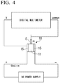
- a circuit of Fig. 4 was assembled using a DC power supply and a multimeter, a constant current of 50 mA was applied between both electrodes 15, and each voltage was measured by bringing an electrode E of a digital multimeter into contact with a side surface of the element body 11 from a position 1 mm away from one electrode 15 to a distance of 9 mm at 1 mm intervals.
- the resistance value was determined from the relationship between the voltage and the current, and a linear approximation was made from the graph of the distance from the electrode end and the resistance value, and an intercept was taken as the electric resistance.
- thermoelectric conversion element was visually observed when taken out from the electric sintering apparatus or after cutting to have the thermoelectric conversion element size, and the presence or absence of a crack was confirmed.
- a Cu amount and a Si amount on the surface of the thermoelectric conversion element were measured by EPMA (JXA-8800RL manufactured by JEOL Ltd.), and the Si/Cu ratio was determined.
- the electrode surface of the cubic sample was polished, and the Cu amount and the Si amount were measured at predetermined five places in the electrode surface by EPMA to determine an average value.
- the measurement point was a cavity or at the end of a particle, a center portion of the particle closest to the measurement point was measured.
- Example 1 Material of electrode Metal layer Si/Cu in raw material (atom number ratio) Si/Cu in electrode (atom number ratio) Thickness of electrode ( ⁇ m) Electric resistance value(Q) Presence or absence of crack during manufacturing Porosity of electrode (%)
- Example 1 Copper silicide - 0.33 0.29 50 0.0038 none 15
- Example 2 Copper silicide - 0.33 0.30 100 0.0034 none 10
- Example 3 Copper silicide - 0.33 0.32 300 0.0035 none 8
- Example 4 Copper silicide - 0.14 0.13 100 0.0037 none 11
- Example 5 Copper silicide - 0.33 0.33 100 0.0033 none 0
- Example 6 Copper silicide Aluminum 0.33 0.31 100 0.0038 none 13
- Example 7 Copper silicide Copper 0.33 0.31 100 0.0034 none 7
- Example 8 Copper silicide Nickel 0.33 0.30 100 0.0039 none 10
- Example 9 Copper silicide - 0.33 0.31 100 0.0062 none 57
- Example 10 Copper silicide - 0.33 0.32 100 0.00
- Comparative Example 1 In Comparative Example 1 in which the electrode was formed of nickel silicide, a crack occurred during manufacturing. Therefore, the electric resistance value and the porosity of the electrode were not evaluated. In Comparative Example 2 in which the electrode was formed of nickel, a crack occurred during manufacturing. Therefore, the electric resistance value and the porosity of the electrode were not evaluated. In Comparative Example 3 in which the electrode was formed of aluminum, no crack occurred during manufacturing, but the electric resistance value was extremely high 0.19 Q.
- thermoelectric conversion element in which an element body formed of a thermoelectric conversion material of a silicide-based compound and an electrode are reliably joined, electric resistance in an interface is sufficiently low, and occurrence of a crack in the element body or the electrode can be suppressed.
- the electric resistance was slightly higher than those of Examples 1 to 10, although lower than that of Comparative Example 3.
- thermoelectric conversion element of the present invention an element body formed of a thermoelectric conversion material of a silicide-based compound and an electrode are reliably joined, electric resistance in an interface is sufficiently low, and occurrence of a crack in the element body or the electrode can be suppressed. Therefore, the present invention is industrially applicable.
Landscapes
- Chemical & Material Sciences (AREA)
- Engineering & Computer Science (AREA)
- Organic Chemistry (AREA)
- Materials Engineering (AREA)
- Ceramic Engineering (AREA)
- Manufacturing & Machinery (AREA)
- Mechanical Engineering (AREA)
- Metallurgy (AREA)
- Structural Engineering (AREA)
- Inorganic Chemistry (AREA)
- Ceramic Products (AREA)
- Powder Metallurgy (AREA)
- Silicon Compounds (AREA)
Abstract
Description
- The present invention relates to a thermoelectric conversion element including an element body formed of a thermoelectric conversion material of a silicide-based compound, and electrodes each formed on one surface of the element body and the other surface opposite the one surface.
- Priority is claimed on Japanese Patent Application No.
2018-049874, filed March 16, 2018 2019-040845, filed March 6, 2019 - A thermoelectric conversion element formed of a thermoelectric conversion material is an electronic element that uses phenomena such as Seebeck effect and Peltier effect and is capable of mutually converting heat and electricity. The Seebeck effect is an effect of converting heat energy into electric energy, and is a phenomenon in which an electromotive force is generated when a temperature difference is generated between both ends of a thermoelectric conversion material. Such an electromotive force depends on characteristics of the thermoelectric conversion material. In recent years, thermoelectric power generation utilizing the effect is actively developed.
- As an index representing a characteristic of the thermoelectric conversion element (thermoelectric conversion material), for example, a power factor (PF) represented by Equation (1) below or a dimensionless performance index (ZT) represented by Equation (2) below is used. In the thermoelectric conversion material, it is necessary to maintain a temperature difference between one surface and the other surface side. Therefore, it is preferable that the thermoelectric conversion material has a low thermal conductivity.

- Here, S: Seebeck coefficient (V/K), σ: Electric conductivity (S/m)

- Examples of the thermoelectric conversion material forming the element body include a silicide-based compound such as magnesium silicide.
- The thermoelectric conversion element described above has a structure in which electrodes are each formed on one end side and the other end side of the thermoelectric conversion material. For the electrode formed on the element body formed of the thermoelectric conversion material of the silicide-based compound such as magnesium silicide, nickel is used. This is because a thermal expansion coefficient of the magnesium silicide (Mg2Si) at room temperature (15.5 × 10⁻⁶ (/°C)) and a thermal expansion coefficient of the nickel at room temperature (15.2 × 10⁻⁶ (/°C)) are approximate.
- However, when the thermoelectric conversion element described above is used at a medium temperature range (300°C or higher and 600°C or lower), Si of the silicide-based compound of the element body diffuses to the electrode side, and nickel of the electrode becomes nickel silicide. Since the nickel silicide has a thermal expansion coefficient of 12.0 × 10⁻⁶ (/°C) at room temperature, a difference in thermal expansion coefficient between the nickel silicide and the element body formed of the thermoelectric conversion material of the silicide-based compound becomes large, and there was a concern that cracks may occur in the element body. In addition, a composition in the vicinity of an interface region of the element body with the electrode changes, and there was a concern that electric resistance increases or strength is reduced.
- Therefore, for example, Patent Document 1 proposes a thermoelectric conversion element in which an intermediate layer formed of a metal silicide with a high melting point is formed between an element body formed of a thermoelectric conversion material and an electrode. In the thermoelectric conversion element, diffusion of an element between the element body and the electrode is suppressed by the intermediate layer formed of the metal silicide with a high melting point.
- In addition, Patent Document 2 proposes a thermoelectric conversion element using a mixture of a nickel silicide and metallic nickel, as an electrode.
-
- [Patent Document 1] Japanese Unexamined Patent Application, First Publication No.
Hei 07-202274 - [Patent Document 2] Republished Japanese Translation No.
WO2012/073946 - However, in the thermoelectric conversion element of Patent Document 1, the intermediate layer formed of the metal silicide with a high melting point is deposited by a vapor deposition method, a sputtering method, or a CVD method, and the intermediate layer could not be formed efficiently. In addition, it was difficult to form the intermediate layer to be thick. Therefore, there was a concern that the intermediate layer cannot sufficiently suppress diffusion of an element of the electrode to the element body.
- In the thermoelectric conversion element of Patent Document 2, the nickel silicide is used as the electrode. However, the nickel silicide has a large difference in thermal expansion coefficient from the element body formed of magnesium silicide or the like, as described above, and there was a concern that a crack may occur in the element body or the electrode due to thermal stress caused by thermal history during manufacturing. Further, in a case where the metallic nickel is in direct contact with the element body formed of magnesium silicide or the like, Si in the element body diffuses to the metallic nickel side and a composition in the vicinity of an interface region of the element body changes. There was a concern that electric resistance increases or strength is reduced.
- The present invention was made in view of circumstances described above, and an object of the present invention is to provide a thermoelectric conversion element in which an element body formed of a thermoelectric conversion material of a silicide-based compound and an electrode are reliably joined, electric resistance in a joining interface is sufficiently low, and occurrence of a crack in the element body or the electrode can be suppressed.
- In order to solve the problems described above, a thermoelectric conversion element of the present invention includes an element body formed of a thermoelectric conversion material of a silicide-based compound; and electrodes each formed on one surface of the element body and the other surface opposite the one surface, in which the electrodes are formed of a sintered body of a copper silicide, and the electrodes and the element body are directly joined.
- According to the thermoelectric conversion element, since the electrodes are formed of the sintered body of the copper silicide, a difference in a thermal expansion coefficient from the element body formed of the thermoelectric conversion material of the silicide-based compound can be reduced. Since the copper silicide has a relatively low melting point, a liquid phase is generated in at least a part of the copper silicide when forming a sintered body to be an electrode, and thermal strain can be released. Accordingly, occurrence of a crack in the element body or the electrode during manufacturing can be suppressed. When forming the sintered body to be an electrode, the entire copper silicide may be in a liquid phase.
- In addition, since the electrodes and the element body are directly joined, and further, as described above, a liquid phase is generated in at least a part of the copper silicide when forming the sintered body to be the electrode, the electrodes and the element body can be sufficiently joined and electric resistance at an interface can be suppressed to be sufficiently low.
- In the thermoelectric conversion element of the present invention, a metal layer may be formed on an opposite surface of the electrode from the element body. In this case, the metal layer formed on the opposite surface from the element body can improve joinability to a terminal.
- In the thermoelectric conversion element of the present invention, it is preferable that a thickness of the electrode is in a range of 10 µm or larger and 300 µm or smaller. In this case, by setting the thickness of the electrode to 300 µm or smaller, rigidity of the electrode does not increase more than necessary, and the occurrence of a crack in the element body during manufacturing can be suppressed. On the other hand, by setting the thickness of the electrode to 10 µm or larger, electric conductivity of the electrode can be secured.
- In the thermoelectric conversion element of the invention, the electrodes are formed of the sintered body of the copper silicide, and it is preferable that an atom number ratio Si/Cu between Si and Cu in the copper silicide is in a range of 0.12 or more and 0.4 or less. In this case, since the atom number ratio Si/Cu between Si and Cu in the copper silicide forming the electrode is in the range of 0.12 or more and 0.4 or less, the electric conductivity of the electrode can be secured high, and the occurrence of a crack in the element body during manufacturing can be suppressed.
- Further, in the thermoelectric conversion element of the present invention, the electrodes are formed of the sintered body of the copper silicide, and it is preferable that a porosity of the copper silicide is 60% or lower. In this case, since the porosity of the copper silicide forming the electrode is set to 60% or lower, an increase in electric resistance can be suppressed.
- According to the present invention, the element body formed of a thermoelectric conversion material of a silicide-based compound and an electrode are reliably joined, electric resistance in an interface is sufficiently low, and occurrence of a crack in the element body or the electrode can be suppressed.
-
-
Fig. 1 is a sectional view showing a thermoelectric conversion element according to a first embodiment of the present invention and a thermoelectric conversion module using the thermoelectric conversion element. -
Fig. 2 is a flowchart showing an example of a method for manufacturing a thermoelectric conversion element according to an embodiment of the present invention. -
Fig. 3 is a sectional view showing an example of a sintering apparatus used in the method for manufacturing a thermoelectric conversion element shown inFig. 2 . -
Fig. 4 is an explanatory view showing means for measuring electric resistance in examples of the present invention. - Hereinafter, a thermoelectric conversion element according to an embodiment of the present invention will be described with reference to accompanying drawings. Each embodiment below is specifically described for better understanding of the gist of the invention, and does not limit the present invention unless otherwise specified. In the drawings used in the following description, for convenience, in order to make the features of the present invention easy to understand, a portion that is a main part may be enlarged in some cases, and a dimensional ratio or the like of each component is not always the same as an actual one.
- A
thermoelectric conversion element 10 according to an embodiment of the present invention will be described with reference toFigs. 1 to 3 .Fig. 1 shows thethermoelectric conversion element 10 according to a first embodiment of the present invention and a thermoelectric conversion module 1 using thethermoelectric conversion element 10. The thermoelectric conversion module 1 shown inFig. 1 includes thethermoelectric conversion element 10 andterminals thermoelectric conversion element 10. - The
thermoelectric conversion element 10 includes anelement body 11 formed of a thermoelectric conversion material, andelectrodes element body 11. As shown inFig. 1 , theelement body 11 is formed in a column shape, andelectrodes element body 11 is not limited, and may be a rectangular parallelepiped, a column, a polygonal column, an elliptical column, or the like. Both surfaces of theelement body 11 to which theelectrodes - A thermoelectric conversion material forming the
element body 11 is formed of, for example, a silicide-based compound. In the present embodiment, the thermoelectric conversion material is preferably formed of a sintered body of magnesium silicide (Mg2Si). Examples of the silicide-based compound that can be used other than the magnesium silicide include silicon germanium (Si-Ge) homogeneous solid solution, manganese silicon (Mn-Si), and iron silicon (Fe-Si). - The thermoelectric conversion material forming the
element body 11 may include at least one of Li, Na, K, B, Al, Ga, In, N, P, As, Sb, Bi, Ag, Cu, and Y, as a dopant. In a case of containing a dopant, a total content thereof in theelement body 11 is preferably 0.1 mass% or more and 3.0 mass% or less, but is not limited to the range. - In the
thermoelectric conversion element 10, theelectrode 15 is formed of a sintered body of copper silicide, and theelectrode 15 and theelement body 11 are directly joined. Theelectrode 15 in this example has the same planar shape as the end surface of theelement body 11. - In addition, in the present embodiment, as shown in
Fig. 1 , ametal layer 16 is formed on an opposite surface of theelectrode 15 from theelement body 11. That is, themetal layer 16 is provided between theelectrode 15 and theterminal 3. Themetal layer 16 in this example has the same planar shape as theelectrode 15. - It is preferable that a thickness of the
electrode 15 formed of the sintered body of the copper silicide is in a range of 10 µm or larger and 300 µm or smaller. If the thickness of theelectrode 15 formed of the sintered body of the copper silicide is 10 µm or larger, electric conductivity of theelectrode 15 can be secured. If the thickness of theelectrode 15 formed of the sintered body of the copper silicide is 300 µm or smaller, the rigidity of theelectrode 15 does not increase more than necessary, and the occurrence of a crack in theelement body 11 during manufacturing can be suppressed. - The lower limit of the thickness of the
electrode 15 formed of the sintered body of the copper silicide is more preferably 50 µm or larger. The upper limit of the thickness of theelectrode 15 formed of the sintered body of the copper silicide is more preferably 150 µm or smaller. - In the copper silicide forming the
electrode 15, an atom number ratio Si/Cu between the Si and Cu is preferably in a range of 0.12 or more and 0.4 or less. - The copper silicide forming the
electrode 15 is obtained by mixing and firing copper silicide powders having a plurality of compositions (Si/Cu), and is adjusted so that an average value thereof is in the range described above. For example, specific examples of copper silicide include Cu3Si (atom number ratio 1/3) or Cu7Si (atom number ratio 1/7), and these can be mixed and used as a sintering raw material. - In a case where the atom number ratio Si/Cu of the copper silicide forming the
electrode 15 is 0.12 or more, the sintering raw material is a copper silicide powder formed by a single phase of Cu7Si or a mixture of Cu7Si and a small amount of a copper silicide having another composition. When melting the entirety or a part of the sintering raw material, electric conduction in theelectrode 15 can be secured and a crack in theelement body 11 can be suppressed. - In a case where the atom number ratio Si/Cu of the copper silicide forming the
electrode 15 is 0.4 or less, the sintering raw material is a copper silicide powder formed by a single phase of Cu3Si or a mixture of Cu3Si and a small amount of a copper silicide having another composition. When melting the entirety or a part of the sintering raw material, electric conduction of theelectrode 15 can be secured and a crack in theelement body 11 during manufacturing can also be suppressed. - A lower limit of the atom number ratio Si/Cu of the copper silicide forming the
electrode 15 is more preferably 0.13 or more. An upper limit of the atom number ratio Si/Cu of copper silicide forming theelectrode 15 is more preferably 0.35 or less. - In the
electrode 15 of the present embodiment, as described above, since copper silicide powders having a plurality of compositions (Si/Cu) are mixed and fired, a liquid phase is formed at least on a part thereof during sintering and theelectrode 15 has a liquid phase solidified portion formed by solidification of the liquid phase on a part thereof. The liquid phase solidified portion has fewer pores and a locally higher density, than a region where the liquid phase is not formed. - The porosity of the
electrode 15 as an entirety is not limited in the present invention, and is preferably 0 volume% or higher and 60 volume% or lower, and more preferably 0 volume% or higher and 50 volume% or lower. The distribution of the liquid phase solidified portion in theelectrode 15 is not limited, and it is preferable that the liquid phase solidified portion is concentrated on theelement body 11 side and distributed in a layered manner, from a viewpoint of stress relaxation. However, in the present invention, the liquid phase solidified portion may be distributed almost uniformly over the entire region in theelectrode 15 or may be concentrated on themetal layer 16 side and distributed in a layered manner. - The porosity of the
electrode 15 was determined by a method below. - First, weight of a silicide sintered body before forming the copper silicide electrode is measured. Then, after the electrodes are formed, the thickness of the electrode on each of both surfaces is measured at five places with an optical microscope or a scanning electron microscope, and an average thereof is determined. Then, the size (such as vertical width, lateral width, and radius) of an electrode surface on each of both surfaces is measured with a caliper or a micrometer, and a surface area of the electrode surface on each of both surfaces is determined. From the surface area and the thickness of the electrode on each of both surfaces, a volume of an electrode part on each of both surfaces is determined. Then, the weight of the silicide sintered body and the electrodes which are in an integrated state is measured, and a weight of the silicide sintered body is subtracted therefrom. Accordingly, the weight of an electrode part is determined. The density of the electrode part is determined from the weight and the volume of the electrode part on both surfaces. The density determined in this manner is defined as a measured density. On the other hand, a true density was estimated and calculated from an average composition obtained by analyzing the electrode layer by EPMA, and a porosity was calculated from a formula of (100 - (Measured density/True density × 100) (%)).
- The
metal layer 16 is formed of, for example, metal excellent in conductivity, such as nickel, aluminum, and copper. In the present embodiment, it is preferable that themetal layer 16 is formed of aluminum. Themetal layer 16 is formed by joining a metal foil or the like to theelectrode 15 by, for example, brazing. The thickness of themetal layer 16 is not limited, and is preferably in a range of 0.1 mm or larger and 2.0 mm or smaller. - The
terminal 3 is formed of a metal material excellent in conductivity, for example, a plate material of copper, aluminum, or the like. In the present embodiment, it is preferable to use a rolled plate of aluminum. Themetal layer 16 formed on theelectrode 15 and theterminal 3 can be joined by, for example, Ag brazing, Ag plating, or the like. The pair ofterminals 3 of the present embodiment extend to opposite sides as viewed from theelement body 11 and are disposed parallel to each other, but the present invention is not limited to this disposition. - Next, an example of a method for manufacturing the
thermoelectric conversion element 10 described above will be described with reference toFigs 2 and3 . - First, a silicide compound powder (magnesium silicide powder) to be a parent phase of the thermoelectric conversion material forming the element body is prepared. In a silicide compound powder preparation step S01, a silicide compound ingot (magnesium silicide) is manufactured, and this ingot is pulverized and sieved to manufacture a silicide compound powder (magnesium silicide powder) having a predetermined particle size. Commercially available magnesium-based compound powder (magnesium silicide powder) may be used. The average particle size of the silicide compound powder (magnesium silicide powder) is preferably in a range of 0.5 µm or larger and 100 µm or smaller.
- Then, the silicide compound powder obtained as described above is heated while pressurizing to obtain a sintered body. In the present embodiment, in an element body sintering step S02, the sintering apparatus (electric sintering apparatus 100) shown in
Fig. 3 is used. - The sintering apparatus (electric sintering apparatus 100) shown in
Fig. 3 includes, for example, a pressure-resistant housing 101, avacuum pump 102 for reducing the pressure inside the pressure-resistant housing 101, and a hollowcylindrical carbon mold 103 disposed inside the pressure-resistant housing 101, a pair ofelectrode portions carbon mold 103 is filled, and apower supply device 106 for applying a voltage between the pair ofelectrode portions carbon plate 107 and acarbon sheet 108 are respectively disposed between theelectrode portions - In the present embodiment, a
heater 109 is provided on an outer peripheral side of thecarbon mold 103. Theheater 109 is disposed on four sides so as to cover the entire surface of thecarbon mold 103 on outer peripheral side. As theheater 109, a carbon heater, a nichrome wire heater, a molybdenum heater, a Kanthal wire heater, a high frequency heater, or the like can be used. - In the element body sintering step S02, first, the
carbon mold 103 of theelectric sintering apparatus 100 shown inFig. 3 is filled with the sintering raw material powder Q. For example, the inside of thecarbon mold 103 is covered with a graphite sheet or a carbon sheet. A direct current is applied between the pair ofelectrode portions power supply device 106, and the current is applied to the sintering raw material powder Q. Accordingly, a temperature increases by self-heating (electric heating). Between the pair ofelectrode portions electrode portion 105a on a movable side is caused to move toward the sintering raw material powder Q, and theheater 109 is heated while pressurizing the sintering raw material powder Q at a predetermined pressure between theelectrode portion 105a and theelectrode portion 105b on a fixed side. Accordingly, the sintering raw material powder Q is sintered by the self-heating of the sintering raw material powder Q, the heat from theheater 109, and the pressurizing. - In the present embodiment, sintering conditions in the element body sintering step S02 are as follows: a heating temperature of the sintering raw material powder Q is in a range of 650°C or higher and 1030°C or lower, and a holding time at the heating temperature is in a range of 0 minutes or longer (for example, 1 second or longer) and 3 minutes or shorter. Pressurizing load is 15 MPa or more and 60 MPa or less. It is preferable that atmosphere in the pressure-
resistant housing 101 is set to an inert atmosphere such as an argon atmosphere or a vacuum atmosphere. When the vacuum atmosphere is set, it is preferable to set the pressure to 5 Pa or less. - In the element body sintering step S02, when the direct current is applied to the sintering raw material powder Q, it is preferable that polarities of the one
electrode portion 105a and theother electrode portion 105b change at a predetermined time interval. In other words, an energizing state in which the oneelectrode portion 105a is used as an anode and theother electrode portion 105b is used as a cathode, and an energizing state in which the oneelectrode portion 105a is used as a cathode and theother electrode portion 105b is used as an anode are performed alternately. In the present embodiment, it is preferable that the predetermined time interval is set in a range of 10 seconds or longer and 300 seconds or shorter. According to the above steps, the element body 11 (thermoelectric conversion material) is manufactured. By alternately switching the direction of the current, an advantage that homogeneity of theelement body 11 is improved can be obtained. - Next, the
carbon mold 103 of theelectric sintering apparatus 100 is filled with the copper silicide powder and the sintered body of the silicide compound. The carbon sheets on both end surfaces and side surfaces of the sintered body of the silicide compound are removed, and both end surfaces of the sintered body are polished with abrasive paper. Thecarbon plate 107 and thecarbon sheet 108 are inserted into thecarbon mold 103, and thecarbon mold 103 is filled with a predetermined amount of copper silicide powder. Thereafter, a sintered body of the silicide compound is inserted thereto, and thecarbon mold 103 is further filled with a predetermined amount of the copper silicide powder thereon. Then, thecarbon plate 107 and thecarbon sheet 108 are disposed thereon. - It is preferable to use a copper silicide powder having an average particle size of 0.5 µm or greater and 50 µm or smaller. In the present embodiment, a mixture of copper silicide powders having a plurality of compositions (mass ratio Si/Cu) is used as the copper silicide powder.
- When a direct current is applied between the pair of
electrode portions power supply device 106 of theelectric sintering apparatus 100, the temperature increases by self-heating (electric heating). Pressurizing is performed at a predetermined pressure by using the pair ofelectrode portions heater 109 is heated. Accordingly, theelectrode 15 is formed by sintering the copper silicide powder, and theelectrode 15 and theelement body 11 are directly joined. - In the present embodiment, sintering conditions in the electrode sintering step S04 are preferably as follows: a heating temperature is in a range of 650°C or higher and 850°C or lower, and a holding time at the heating temperature is in a range of 0 minutes or longer (for example, 1 second or longer) and 3 minutes or shorter. It is preferable that pressurizing load is in a range of 2 MPa or more and 40 MPa or less. It is preferable that an atmosphere in the pressure-
resistant housing 101 is set to an inert atmosphere such as an argon atmosphere or a vacuum atmosphere. In a case where the vacuum atmosphere is set, it is preferable that the pressure is set to 5 Pa or less. - In the present embodiment, since a mixture of the copper silicide powders having a plurality of compositions (atom number ratio Si/Cu) is used as the copper silicide powder, a liquid phase is generated on a part in the electrode sintering step S04, and a liquid phase solidified portion formed by solidification of the liquid phase on a part of the
electrode 15 is formed. The generation of the liquid phase in the electrode sintering step S04 improves joinability between theelement body 11 and theelectrode 15. - Next, a
metal layer 16 is formed on an opposite surface of theelectrode 15 from theelement body 11. Themetal layer 16 can be formed by joining a metal foil material excellent in conductivity, such as nickel, aluminum, or copper, to theelectrode 15 by using, for example, a brazing material. As the brazing material, Ag brazing such as Ag-Cu-Zn-Cd and Ag-Cu-Sn can be used. - In the present embodiment, a rolled plate of aluminum, having a thickness of 0.5 mm is cut into the same size as a section of the thermoelectric element, and a
metal layer 16 is formed on theelectrode 15 using Ag brazing (BAg-lA (JIS)). - According to the steps, the
thermoelectric conversion element 10 in which theelement body 11 formed of the thermoelectric conversion material of the silicide-based compound and theelectrode 15 formed of the sintered body of the copper silicide are directly joined is manufactured. - According to the
thermoelectric conversion element 10 described above, since theelectrode 15 is formed of the sintered body of the copper silicide, a difference in a thermal expansion coefficient from theelement body 11 formed of the thermoelectric conversion material of the silicide-based compound (magnesium silicide) can be reduced, and occurrence of a crack due to thermal history during manufacturing or using can be suppressed. - In addition, since the copper silicide has a relatively low melting point, a liquid phase is generated on a part when forming the sintered body, and thermal strain can be released. The occurrence of a crack in the
element body 11 and theelectrode 15 during manufacturing can be suppressed. - Further, the
electrode 15 and theelement body 11 are directly joined, and a liquid phase is generated on a part when forming the sintered body. Accordingly, the joinability between theelectrode 15 and theelement body 11 is improved. Therefore, electric resistance at an interface can be suppressed to be sufficiently low. - Further, in the present embodiment, since the
metal layer 16 is formed on the opposite surface of theelectrode 15 from theelement body 11, theterminal 3 and theelectrode 15 can be relatively easily joined and joinability between the terminal 3 and theelectrode 15 can be improved. - In addition, in the present embodiment, since the thickness of the
electrode 15 is in the range of 10 µm or larger and 300 µm or smaller, the rigidity of theelectrode 15 does not increase more than necessary, and the occurrence of a crack in theelement body 11 during manufacturing can be suppressed. Also, the electric conductivity of theelectrode 15 can be secured. - Further, in the present embodiment, since the atom number ratio Si/Cu between Si and Cu in the copper silicide forming the
electrode 15 is in the range of 0.12 or more and 0.4 or less, the electric conductivity of theelectrode 15 can be secured, and the occurrence of a crack in theelement body 11 during manufacturing can be suppressed. - As described above, the embodiments of the present invention are described. However, the present invention is not limited thereto, and can be appropriately modified without departing from the technical idea of the present invention. For example, in the present embodiment, it was described that the thermoelectric conversion element and the thermoelectric conversion module having a structure as shown in
Fig. 1 are configured. However, the present invention is not limited thereto, and there is no particular limitation on a structure and disposition of the terminals, as long as the thermoelectric conversion element of the present invention is used. - In addition, in the present embodiment, it was described that the silicide-based compound forming element body is the magnesium silicide (Mg2Si). However, the present invention is not limited thereto, and a silicide-based compound having another composition may be used, as long as the compound has a thermoelectric property.
- In addition, in the embodiment, a mixture of the copper silicide powders having a plurality of compositions (atom number ratio Si/Cu) is used as the copper silicide powder. However, the present invention is not limited thereto, and a copper silicide powder having a single composition can be used. In this case, the entire electrode can be easily made into a liquid phase and joined to the element body, by controlling the sintering temperature in the electrode sintering step. In this case, since the entire electrode becomes a liquid phase, it is difficult for the electrode to be peeled off from the element body, and the conductivity can also be secured.
- Hereinafter, results of experiments performed to confirm the effects of the present invention will be described.
- A columnar element body (size: diameter 20 mm ×
thickness 10 mm) formed of a sintered body (porosity 2 volume%) of magnesium silicide (Mg2Si) was prepared. Using the electric sintering apparatus shown inFig. 3 described in the above embodiment, both surfaces of the element body are filled with powders of materials shown in Table 1 and electric sintering is performed by the above-described method. Electrodes having a constant thickness were formed on both ends of the element body. Accordingly, the thermoelectric conversion elements of Examples 1 to 11 and Comparative Examples 1 to 3 were manufactured. The porosity of the electrode was shown in Table 1. Except for Example 5, a plurality of copper silicide powders having different Si/Cu ratios were mixed and used to obtain ratios shown in Table 1. In Example 5, a copper silicide powder having a single composition having the Si/Cu ratio shown in Table 1 was used. - For the obtained thermoelectric conversion elements of Examples and Comparative Examples, an electric resistance value, the presence or absence of a crack during manufacturing, and a Si/Cu ratio of the electrode were evaluated as follows.
- A
cubic sample 10 of 10 mm × 10 mm × 10 mm was cut out from the obtained thermoelectric conversion element and used for evaluation. To measure the electric resistance value, a circuit ofFig. 4 was assembled using a DC power supply and a multimeter, a constant current of 50 mA was applied between bothelectrodes 15, and each voltage was measured by bringing an electrode E of a digital multimeter into contact with a side surface of theelement body 11 from a position 1 mm away from oneelectrode 15 to a distance of 9 mm at 1 mm intervals. Next, the resistance value was determined from the relationship between the voltage and the current, and a linear approximation was made from the graph of the distance from the electrode end and the resistance value, and an intercept was taken as the electric resistance. - Regarding the presence or absence of a crack during manufacturing, after the electrodes were formed by electric sintering, the thermoelectric conversion element was visually observed when taken out from the electric sintering apparatus or after cutting to have the thermoelectric conversion element size, and the presence or absence of a crack was confirmed.
- Regarding the Si/Cu ratio of the electrode, a Cu amount and a Si amount on the surface of the thermoelectric conversion element (the surface on which the electrode was formed) were measured by EPMA (JXA-8800RL manufactured by JEOL Ltd.), and the Si/Cu ratio was determined.
- Specifically, the electrode surface of the cubic sample was polished, and the Cu amount and the Si amount were measured at predetermined five places in the electrode surface by EPMA to determine an average value. In a case where the measurement point was a cavity or at the end of a particle, a center portion of the particle closest to the measurement point was measured.
[Table 1] Material of electrode Metal layer Si/Cu in raw material (atom number ratio) Si/Cu in electrode (atom number ratio) Thickness of electrode (µm) Electric resistance value(Q) Presence or absence of crack during manufacturing Porosity of electrode (%) Example 1 Copper silicide - 0.33 0.29 50 0.0038 none 15 Example 2 Copper silicide - 0.33 0.30 100 0.0034 none 10 Example 3 Copper silicide - 0.33 0.32 300 0.0035 none 8 Example 4 Copper silicide - 0.14 0.13 100 0.0037 none 11 Example 5 Copper silicide - 0.33 0.33 100 0.0033 none 0 Example 6 Copper silicide Aluminum 0.33 0.31 100 0.0038 none 13 Example 7 Copper silicide Copper 0.33 0.31 100 0.0034 none 7 Example 8 Copper silicide Nickel 0.33 0.30 100 0.0039 none 10 Example 9 Copper silicide - 0.33 0.31 100 0.0062 none 57 Example 10 Copper silicide - 0.33 0.32 100 0.0047 none 8 Example 11 Copper silicide - 0.33 0.31 100 0.0097 none 66 Comparative example 1 Nickel silicide - - - 100 - occurred - Comparative example 2 Nickel - - - 100 - occurred - Comparative example 3 Aluminum - - - 100 0.1900 none 45 - In Comparative Example 1 in which the electrode was formed of nickel silicide, a crack occurred during manufacturing. Therefore, the electric resistance value and the porosity of the electrode were not evaluated. In Comparative Example 2 in which the electrode was formed of nickel, a crack occurred during manufacturing. Therefore, the electric resistance value and the porosity of the electrode were not evaluated. In Comparative Example 3 in which the electrode was formed of aluminum, no crack occurred during manufacturing, but the electric resistance value was extremely high 0.19 Q.
- On the other hand, in Examples 1 to 11 in which the electrodes were formed of copper silicide, no cracks occurred during manufacturing and the electric resistance value was low.
- From the above, it was confirmed that, according to Examples 1 to 11, it is possible to provide a thermoelectric conversion element in which an element body formed of a thermoelectric conversion material of a silicide-based compound and an electrode are reliably joined, electric resistance in an interface is sufficiently low, and occurrence of a crack in the element body or the electrode can be suppressed. In Example 11 in which the porosity exceeded 60%, the electric resistance was slightly higher than those of Examples 1 to 10, although lower than that of Comparative Example 3.
- According to the thermoelectric conversion element of the present invention, an element body formed of a thermoelectric conversion material of a silicide-based compound and an electrode are reliably joined, electric resistance in an interface is sufficiently low, and occurrence of a crack in the element body or the electrode can be suppressed. Therefore, the present invention is industrially applicable.
-
- 1 Thermoelectric conversion module
- 3 Terminal
- 10 Thermoelectric conversion element
- 11 Element body
- 15 Electrode
- 16 Metal layer
Claims (5)
- A thermoelectric conversion element comprising:an element body formed of a thermoelectric conversion material of a silicide-based compound; andelectrodes each formed on one surface of the element body and the other surface opposite the one surface,wherein the electrodes are formed of a sintered body of a copper silicide, andthe electrodes and the element body are directly joined.
- The thermoelectric conversion element according to claim 1,
wherein a metal layer is formed on an opposite surface of the electrode, from the element body. - The thermoelectric conversion element according to claim 1 or 2,
wherein a thickness of the electrode is 10 µm or larger and 300 µm or smaller. - Thermoelectric conversion element according to claims 1 to 3,
wherein an atom number ratio Si/Cu between Si and Cu in the copper silicide is 0.12 or more and 0.4 or less. - The thermoelectric conversion element according to any one of claims 1 to 4,
wherein a porosity of the copper silicide is 60% or lower.
Applications Claiming Priority (3)
| Application Number | Priority Date | Filing Date | Title |
|---|---|---|---|
| JP2018049874 | 2018-03-16 | ||
| JP2019040845A JP7242999B2 (en) | 2018-03-16 | 2019-03-06 | Thermoelectric conversion element |
| PCT/JP2019/010818 WO2019177147A1 (en) | 2018-03-16 | 2019-03-15 | Thermoelectric conversion element |
Publications (2)
| Publication Number | Publication Date |
|---|---|
| EP3767689A1 true EP3767689A1 (en) | 2021-01-20 |
| EP3767689A4 EP3767689A4 (en) | 2021-12-01 |
Family
ID=68065018
Family Applications (1)
| Application Number | Title | Priority Date | Filing Date |
|---|---|---|---|
| EP19768346.9A Withdrawn EP3767689A4 (en) | 2018-03-16 | 2019-03-15 | THERMOELECTRIC CONVERSION ELEMENT |
Country Status (5)
| Country | Link |
|---|---|
| US (1) | US11152554B2 (en) |
| EP (1) | EP3767689A4 (en) |
| JP (1) | JP7242999B2 (en) |
| KR (1) | KR20200130806A (en) |
| CN (1) | CN111630672A (en) |
Families Citing this family (3)
| Publication number | Priority date | Publication date | Assignee | Title |
|---|---|---|---|---|
| KR102872812B1 (en) * | 2021-07-12 | 2025-10-21 | 엘지이노텍 주식회사 | Thermoelectric module |
| JPWO2024048172A1 (en) * | 2022-08-29 | 2024-03-07 | ||
| CN119769214A (en) * | 2022-08-29 | 2025-04-04 | 松下知识产权经营株式会社 | Thermoelectric conversion element and manufacturing method thereof, bonding material, thermoelectric conversion module, thermoelectric conversion system, and power generation method |
Family Cites Families (26)
| Publication number | Priority date | Publication date | Assignee | Title |
|---|---|---|---|---|
| JP2749134B2 (en) * | 1989-07-12 | 1998-05-13 | 宇部興産株式会社 | Powder for thermoelectric conversion material and sintered body thereof |
| JP3152254B2 (en) * | 1992-04-28 | 2001-04-03 | 宇部興産株式会社 | Powder for thermoelectric conversion materials |
| JP3216378B2 (en) | 1993-12-28 | 2001-10-09 | 日産自動車株式会社 | Thermoelectric device and method of manufacturing the same |
| JPH08148726A (en) * | 1994-09-22 | 1996-06-07 | Ngk Spark Plug Co Ltd | Thermoelectric conversion element and manufacturing method thereof |
| EP1227353B1 (en) * | 2001-01-16 | 2005-05-04 | Curamik Electronics GmbH | Laser mirror and method for manufacturing the same |
| JP2003234516A (en) * | 2002-02-12 | 2003-08-22 | Komatsu Ltd | Thermoelectric module |
| JP2004349566A (en) * | 2003-05-23 | 2004-12-09 | Kyocera Corp | Unidirectionally solidified thermoelectric crystal material and method of manufacturing the same, thermoelectric element using the same, method of manufacturing the same, and thermoelectric module |
| JP4570071B2 (en) * | 2004-04-30 | 2010-10-27 | 日立粉末冶金株式会社 | Thermoelectric conversion module and manufacturing method thereof |
| CN1969398A (en) * | 2004-06-17 | 2007-05-23 | 阿鲁策株式会社 | Thermoelectric conversion module |
| JP4584035B2 (en) * | 2005-05-31 | 2010-11-17 | トヨタ自動車株式会社 | Thermoelectric module |
| JP4584034B2 (en) * | 2005-05-31 | 2010-11-17 | トヨタ自動車株式会社 | Thermoelectric module |
| JP2008300465A (en) * | 2007-05-30 | 2008-12-11 | Showa Denko Kk | Method of joining thermoelectric element and electrode and method of manufacturing thermoelectric module |
| JP2009117645A (en) * | 2007-11-07 | 2009-05-28 | Showa Denko Kk | Electrode for thermoelectric element and thermoelectric module |
| JP5439723B2 (en) * | 2008-01-22 | 2014-03-12 | セイコーエプソン株式会社 | Thin film transistor, matrix substrate, electrophoretic display device and electronic device |
| JP2009302332A (en) * | 2008-06-13 | 2009-12-24 | Aruze Corp | Thermoelectric conversion element and conductive member for thermoelectric conversion element |
| JP2013510417A (en) * | 2009-11-03 | 2013-03-21 | ビーエーエスエフ ソシエタス・ヨーロピア | Use of porous metal materials as contact connections for thermoelectric modules |
| WO2012073946A1 (en) * | 2010-11-30 | 2012-06-07 | 学校法人東京理科大学 | Thermoelectric conversion element and thermoelectric conversion module |
| CN103311423B (en) * | 2012-02-17 | 2017-06-30 | 雅马哈株式会社 | The manufacture method of thermoelectric conversion component and thermoelectric conversion component |
| JP2013201382A (en) * | 2012-03-26 | 2013-10-03 | Nagoya Univ | Thermoelectric conversion module and method for manufacturing the same |
| KR20170026323A (en) * | 2014-03-25 | 2017-03-08 | 실리시움 에너지, 인크. | Thermoelectric devices and systems |
| JP6188635B2 (en) * | 2014-05-28 | 2017-08-30 | 株式会社日立製作所 | Thermoelectric conversion material and thermoelectric conversion element |
| JP6382093B2 (en) * | 2014-12-17 | 2018-08-29 | 古河電気工業株式会社 | Thermoelectric conversion element and thermoelectric conversion module |
| FR3040239B1 (en) * | 2015-08-21 | 2018-08-03 | Universite De Lorraine | IMPROVED THERMOELECTRIC ELEMENT AND THERMOELECTRIC CONVERTER COMPRISING SUCH AN ELEMENT. |
| JP6794732B2 (en) * | 2015-09-28 | 2020-12-02 | 三菱マテリアル株式会社 | Thermoelectric conversion module and thermoelectric conversion device |
| WO2017096094A1 (en) * | 2015-12-01 | 2017-06-08 | Silicium Energy, Inc. | Thermoelectric devices and systems |
| US10153351B2 (en) * | 2016-01-29 | 2018-12-11 | Taiwan Semiconductor Manufacturing Co., Ltd. | Semiconductor device and a method for fabricating the same |
-
2019
- 2019-03-06 JP JP2019040845A patent/JP7242999B2/en active Active
- 2019-03-15 US US16/957,968 patent/US11152554B2/en not_active Expired - Fee Related
- 2019-03-15 CN CN201980007644.4A patent/CN111630672A/en active Pending
- 2019-03-15 KR KR1020207019226A patent/KR20200130806A/en not_active Withdrawn
- 2019-03-15 EP EP19768346.9A patent/EP3767689A4/en not_active Withdrawn
Also Published As
| Publication number | Publication date |
|---|---|
| US11152554B2 (en) | 2021-10-19 |
| JP2019165215A (en) | 2019-09-26 |
| JP7242999B2 (en) | 2023-03-22 |
| US20200373474A1 (en) | 2020-11-26 |
| KR20200130806A (en) | 2020-11-20 |
| EP3767689A4 (en) | 2021-12-01 |
| CN111630672A (en) | 2020-09-04 |
Similar Documents
| Publication | Publication Date | Title |
|---|---|---|
| US11647674B2 (en) | Thermoelectric conversion material, thermoelectric conversion element, thermoelectric conversion module, and method for manufacturing thermoelectric conversion material | |
| EP3432371B1 (en) | Magnesium-based thermoelectric conversion material, magnesium-based thermoelectric conversion element, thermoelectric conversion device, and method for manufacturing magnesium-based thermoelectric conversion material | |
| KR20180114892A (en) | A method of manufacturing a magnesium-based thermoelectric conversion material, a method of manufacturing a magnesium-based thermoelectric conversion element, a magnesium-based thermoelectric conversion material, a magnesium-based thermoelectric conversion element, | |
| JP7121230B2 (en) | Method for producing magnesium-based thermoelectric conversion material | |
| US11152554B2 (en) | Thermoelectric conversion element | |
| US9627600B2 (en) | Mg—Si system thermoelectric conversion material, method for producing same, sintered body for thermoelectric conversion, thermoelectric conversion element, and thermoelectric conversion module | |
| EP3428983B1 (en) | Method for producing thermoelectric conversion material | |
| JP7251187B2 (en) | Thermoelectric conversion material, thermoelectric conversion element, thermoelectric conversion module, and method for producing thermoelectric conversion material | |
| KR102409289B1 (en) | Magnesium-based thermoelectric conversion material, magnesium-based thermoelectric conversion element, and manufacturing method of magnesium-based thermoelectric conversion material | |
| US12114572B2 (en) | Compound and thermoelectric conversion material | |
| EP3758080A1 (en) | Thermoelectric conversion material, thermoelectric conversion element, and thermoelectric conversion module | |
| EP3648185B1 (en) | Thermoelectric conversion material, thermoelectric conversion element, thermoelectric conversion module, and method for manufacturing thermoelectric conversion material | |
| WO2019177147A1 (en) | Thermoelectric conversion element | |
| EP4123733A1 (en) | Thermoelectric conversion material, thermoelectric conversion element, and thermoelectric conversion module | |
| WO2014162726A1 (en) | Thermoelectric conversion material | |
| WO2019168029A1 (en) | Thermoelectric conversion material, thermoelectric conversion element, thermoelectric conversion module and method for producing thermoelectric conversion material | |
| JP7631702B2 (en) | Thermoelectric conversion material, thermoelectric conversion element, and thermoelectric conversion module | |
| US20230043063A1 (en) | Thermoelectric conversion material, thermoelectric conversion element, and thermoelectric conversion module | |
| US20220013703A1 (en) | Thermoelectric conversion material, thermoelectric conversion element, and thermoelectric conversion module |
Legal Events
| Date | Code | Title | Description |
|---|---|---|---|
| STAA | Information on the status of an ep patent application or granted ep patent |
Free format text: STATUS: THE INTERNATIONAL PUBLICATION HAS BEEN MADE |
|
| PUAI | Public reference made under article 153(3) epc to a published international application that has entered the european phase |
Free format text: ORIGINAL CODE: 0009012 |
|
| STAA | Information on the status of an ep patent application or granted ep patent |
Free format text: STATUS: REQUEST FOR EXAMINATION WAS MADE |
|
| 17P | Request for examination filed |
Effective date: 20200624 |
|
| AK | Designated contracting states |
Kind code of ref document: A1 Designated state(s): AL AT BE BG CH CY CZ DE DK EE ES FI FR GB GR HR HU IE IS IT LI LT LU LV MC MK MT NL NO PL PT RO RS SE SI SK SM TR |
|
| AX | Request for extension of the european patent |
Extension state: BA ME |
|
| DAV | Request for validation of the european patent (deleted) | ||
| DAX | Request for extension of the european patent (deleted) | ||
| A4 | Supplementary search report drawn up and despatched |
Effective date: 20211102 |
|
| RIC1 | Information provided on ipc code assigned before grant |
Ipc: H01L 35/22 20060101ALI20211026BHEP Ipc: C22C 28/00 20060101ALI20211026BHEP Ipc: C22C 23/00 20060101ALI20211026BHEP Ipc: C04B 37/02 20060101ALI20211026BHEP Ipc: C04B 35/645 20060101ALI20211026BHEP Ipc: B32B 15/01 20060101ALI20211026BHEP Ipc: H01L 35/34 20060101ALI20211026BHEP Ipc: H01L 35/14 20060101ALI20211026BHEP Ipc: C22C 9/10 20060101ALI20211026BHEP Ipc: C22C 1/05 20060101ALI20211026BHEP Ipc: C04B 35/58 20060101ALI20211026BHEP Ipc: H01L 35/08 20060101AFI20211026BHEP |
|
| REG | Reference to a national code |
Ref country code: DE Ref legal event code: R079 Free format text: PREVIOUS MAIN CLASS: H01L0035080000 Ipc: B32B0015010000 |
|
| GRAP | Despatch of communication of intention to grant a patent |
Free format text: ORIGINAL CODE: EPIDOSNIGR1 |
|
| RIC1 | Information provided on ipc code assigned before grant |
Ipc: H10N 10/855 20230101ALN20230223BHEP Ipc: H10N 10/817 20230101ALI20230223BHEP Ipc: C22C 28/00 20060101ALI20230223BHEP Ipc: C22C 23/00 20060101ALI20230223BHEP Ipc: C22C 9/10 20060101ALI20230223BHEP Ipc: C04B 37/02 20060101ALI20230223BHEP Ipc: C04B 35/645 20060101ALI20230223BHEP Ipc: C04B 35/58 20060101ALI20230223BHEP Ipc: B32B 15/01 20060101AFI20230223BHEP |
|
| STAA | Information on the status of an ep patent application or granted ep patent |
Free format text: STATUS: GRANT OF PATENT IS INTENDED |
|
| INTG | Intention to grant announced |
Effective date: 20230330 |
|
| STAA | Information on the status of an ep patent application or granted ep patent |
Free format text: STATUS: THE APPLICATION IS DEEMED TO BE WITHDRAWN |
|
| 18D | Application deemed to be withdrawn |
Effective date: 20230810 |