EP3764203B1 - Signalübertragungsverfahren und -system, aktiver eingabestift, berührungsbildschirm und lesbares speichermedium - Google Patents
Signalübertragungsverfahren und -system, aktiver eingabestift, berührungsbildschirm und lesbares speichermedium Download PDFInfo
- Publication number
- EP3764203B1 EP3764203B1 EP19920633.5A EP19920633A EP3764203B1 EP 3764203 B1 EP3764203 B1 EP 3764203B1 EP 19920633 A EP19920633 A EP 19920633A EP 3764203 B1 EP3764203 B1 EP 3764203B1
- Authority
- EP
- European Patent Office
- Prior art keywords
- signal
- circuit
- dsss
- inverting
- resistor
- Prior art date
- Legal status (The legal status is an assumption and is not a legal conclusion. Google has not performed a legal analysis and makes no representation as to the accuracy of the status listed.)
- Active
Links
Images






Classifications
-
- G—PHYSICS
- G06—COMPUTING OR CALCULATING; COUNTING
- G06F—ELECTRIC DIGITAL DATA PROCESSING
- G06F3/00—Input arrangements for transferring data to be processed into a form capable of being handled by the computer; Output arrangements for transferring data from processing unit to output unit, e.g. interface arrangements
- G06F3/01—Input arrangements or combined input and output arrangements for interaction between user and computer
- G06F3/03—Arrangements for converting the position or the displacement of a member into a coded form
- G06F3/033—Pointing devices displaced or positioned by the user, e.g. mice, trackballs, pens or joysticks; Accessories therefor
- G06F3/0354—Pointing devices displaced or positioned by the user, e.g. mice, trackballs, pens or joysticks; Accessories therefor with detection of two-dimensional [2D] relative movements between the device, or an operating part thereof, and a plane or surface, e.g. 2D mice, trackballs, pens or pucks
- G06F3/03545—Pens or stylus
-
- G—PHYSICS
- G06—COMPUTING OR CALCULATING; COUNTING
- G06F—ELECTRIC DIGITAL DATA PROCESSING
- G06F3/00—Input arrangements for transferring data to be processed into a form capable of being handled by the computer; Output arrangements for transferring data from processing unit to output unit, e.g. interface arrangements
- G06F3/01—Input arrangements or combined input and output arrangements for interaction between user and computer
- G06F3/03—Arrangements for converting the position or the displacement of a member into a coded form
- G06F3/033—Pointing devices displaced or positioned by the user, e.g. mice, trackballs, pens or joysticks; Accessories therefor
- G06F3/0354—Pointing devices displaced or positioned by the user, e.g. mice, trackballs, pens or joysticks; Accessories therefor with detection of two-dimensional [2D] relative movements between the device, or an operating part thereof, and a plane or surface, e.g. 2D mice, trackballs, pens or pucks
-
- G—PHYSICS
- G06—COMPUTING OR CALCULATING; COUNTING
- G06F—ELECTRIC DIGITAL DATA PROCESSING
- G06F3/00—Input arrangements for transferring data to be processed into a form capable of being handled by the computer; Output arrangements for transferring data from processing unit to output unit, e.g. interface arrangements
- G06F3/01—Input arrangements or combined input and output arrangements for interaction between user and computer
- G06F3/03—Arrangements for converting the position or the displacement of a member into a coded form
- G06F3/033—Pointing devices displaced or positioned by the user, e.g. mice, trackballs, pens or joysticks; Accessories therefor
- G06F3/038—Control and interface arrangements therefor, e.g. drivers or device-embedded control circuitry
- G06F3/0383—Signal control means within the pointing device
-
- G—PHYSICS
- G06—COMPUTING OR CALCULATING; COUNTING
- G06F—ELECTRIC DIGITAL DATA PROCESSING
- G06F3/00—Input arrangements for transferring data to be processed into a form capable of being handled by the computer; Output arrangements for transferring data from processing unit to output unit, e.g. interface arrangements
- G06F3/01—Input arrangements or combined input and output arrangements for interaction between user and computer
- G06F3/03—Arrangements for converting the position or the displacement of a member into a coded form
- G06F3/041—Digitisers, e.g. for touch screens or touch pads, characterised by the transducing means
- G06F3/0416—Control or interface arrangements specially adapted for digitisers
- G06F3/04162—Control or interface arrangements specially adapted for digitisers for exchanging data with external devices, e.g. smart pens, via the digitiser sensing hardware
-
- G—PHYSICS
- G06—COMPUTING OR CALCULATING; COUNTING
- G06F—ELECTRIC DIGITAL DATA PROCESSING
- G06F3/00—Input arrangements for transferring data to be processed into a form capable of being handled by the computer; Output arrangements for transferring data from processing unit to output unit, e.g. interface arrangements
- G06F3/01—Input arrangements or combined input and output arrangements for interaction between user and computer
- G06F3/03—Arrangements for converting the position or the displacement of a member into a coded form
- G06F3/041—Digitisers, e.g. for touch screens or touch pads, characterised by the transducing means
- G06F3/044—Digitisers, e.g. for touch screens or touch pads, characterised by the transducing means by capacitive means
- G06F3/0441—Digitisers, e.g. for touch screens or touch pads, characterised by the transducing means by capacitive means using active external devices, e.g. active pens, for receiving changes in electrical potential transmitted by the digitiser, e.g. tablet driving signals
Definitions
- the present disclosure relates to touch technologies, and more particularly, to a method and a system for transmitting a signal, an active stylus, a touch screen and a readable storage medium.
- a touch screen may send a direct sequence spread spectrum (DSSS) signal to a stylus end to communicate with the stylus end, so as to perform operations such as synchronizing with the stylus end and sending a command to the stylus end.
- DSSS direct sequence spread spectrum
- DSSS signal transmission is usually applied in a radio frequency environment, that is, the DSSS signal is transmitted and received through a high-frequency antenna.
- conditions such as impedance of a screen sensor itself limit spectrum spreading of the DSSS signal, so a mode of transmitting and receiving the DSSS signal through the high-frequency antenna is not applicable to the active stylus touch system that has strict requirements on a structure, a size and power consumption, and the like.
- a patent application US 20170192534A1 discloses relevant technologies regarding to the active stylus pen
- a patent application US 20160226540A1 discloses relevant technologies regarding to a reception circuit
- paper "Implementation and Experimental Demonstration of A Real-time 7-DSSS VLC System Based on FPGA” discloses relevant technologies regarding to using the 7-DSSS technique in VLC system.
- a first embodiment of the present disclosure relates to a method for transmitting a signal, applied to products such as a mobile phone, a tablet personal computer and a computer which have an active stylus and a touch function.
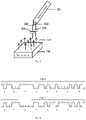
- FIG. 1 shows an application scenario of the method for transmitting a signal according to this embodiment.
- FIG. 1 shows an application scenario of the method for transmitting a signal according to this embodiment.
- a touch screen 104 and an electrode 102 of an active stylus 101 may form a coupling capacitor 103
- the touch screen 104 may use a transmitting (TX)/ receiving (RX) sensor to send a DSSS signal
- the active stylus 101 uses the coupling capacitor 103 to receive the DSSS signal sent by the touch screen 104, and then parses the DSSS signal, so as to implement information interaction between the active stylus 101 and the touch screen 104.
- a flow chart of the method for transmitting a signal according to this embodiment may be as shown in FIG. 2 and include the following steps.
- the DSSS signal sent by the touch screen is received through the coupling capacitor formed between the active stylus and the touch screen.
- the touch screen may perform spread-spectrum coding on a signal to be transmitted to generate the DSSS signal, the touch screen may use the TX/RX sensor to send the DSSS signal, and the active stylus uses the coupling capacitor to receive the DSSS signal sent by the touch screen.
- the coupling capacitor formed between the active stylus and the touch screen may be the coupling capacitor 103 shown in FIG. 1 .
- FIG. 3 also shows a schematic diagram of the coupling capacitor formed between the active stylus and the touch screen.
- the active stylus 101 includes a main electrode 302 and a secondary electrode 303, and the coupling capacitor formed between the active stylus and the touch screen includes: a coupling capacitor 305 formed between the main electrode 302 and the touch screen 104, or a coupling capacitor 306 formed between the secondary electrode 303 and the touch screen 104.
- the active stylus 101 may receive the DSSS signal through the coupling capacitor 305, or may also receive the DSSS signal through the coupling capacitor 306.
- a spread-spectrum coded form of DSSS signals corresponding to "0" and "1" in the USI may be adopted.
- "0” is represented by a 31-bit code 0x58F9A42B
- "1” is represented by a 31-bit code 0x27065BD4
- a duration for which each bit lasts is 1 us.
- This embodiment only takes spread-spectrum coding of DSSS signals in the USI as an example, but is not limited to such type of spread-spectrum coding in the actual application.
- the received DSSS signal is parsed to obtain the signal to be transmitted.
- the DSSS signal received by the active stylus through a coupling capacitor 501 is input to a Comparator Counter DSSS Mixer (CCDM) parsing system 502 in the active stylus, and the CCDM parsing system 502 parses the received DSSS signal to obtain the signal to be transmitted.
- CCDM Comparator Counter DSSS Mixer
- the CCDM parsing system 502 includes: a pre-amplifier circuit 503, a hysteresis comparing circuit 504, and a digital demodulating circuit 505.
- the pre-amplifier circuit 503 pre-amplifies the received DSSS signal, and inputs the pre-amplified DSSS signal into the hysteresis comparing circuit 504.
- the hysteresis comparing circuit 504 restores the pre-amplified DSSS signal to obtain a restored DSSS signal, and inputs the restored DSSS signal into the digital demodulating circuit 505.
- the digital demodulating circuit 505 demodulates the restored DSSS signal, and parses out specific coding information of the DSSS signal, that is, the signal to be transmitted.
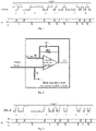
- the pre-amplifier circuit 503 may be an Analog Front End (AFE) circuit, and the AFE circuit may be an inverting amplifier circuit, for example, a low-impedance inverting amplifier circuit shown in FIG. 6 .
- the DSSS signal is used as an input signal of an inverting input end of an operational amplifier (OPA) in the low-impedance inverting amplifier circuit.
- OPA operational amplifier
- a waveform diagram of the input signal and an output signal of the low-impedance inverting amplifier circuit may be as shown in FIG. 7 .
- the input signal is a DSSS signal coded according to the USI, with code 0 as an example, and the output signal is an inverting amplified signal VI.
- VP is a positive output amplitude of the inverting amplified signal
- VN is a negative output amplitude of the inverting amplified signal
- Voltage Common Mode Input (VCMI) is a common mode input voltage
- an output amplitude of the inverting amplified signal may be controlled by configuring parameters of devices such as a resistor and a capacitor in the diagram.
- the AFE circuit may be a non-inverting amplifier circuit, for example, a high-impedance non-inverting amplifier circuit as shown in FIG. 8 .
- the DSSS signal is used as an input signal of a non-inverting input end of an OPA in the high-impedance non-inverting amplifier circuit.
- a waveform diagram of the input signal and an output signal of the high-impedance non-inverting amplifier circuit may be as shown in FIG. 9 .
- the input signal is a DSSS signal coded according to the USI protocol, with code 1 as an example, and the output signal is a non-inverting amplified signal VI, and an output amplitude of the inverting amplified signal may be controlled by configuring parameters of devices such as a resistor and a capacitor in the diagram.
- the hysteresis comparing circuit 504 may be a non-inverting hysteresis comparing circuit or an inverting hysteresis comparing circuit, and the hysteresis comparing circuit 504 will be specifically described below with two examples.
- the hysteresis comparing circuit 504 may be a non-inverting hysteresis comparing circuit in FIG. 10 .
- the non-inverting hysteresis comparing circuit may restore the pre-amplified signal to an original DSSS signal.
- VI as the output signal of the AFE circuit, is used as an input signal of a non-inverting end of a comparator in the hysteresis comparing circuit 504, and V2 is an output signal of the hysteresis comparing circuit.
- a waveform diagram of the input signal and an output signal of the non-inverting hysteresis comparing circuit may be as shown in FIG.
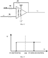
- the hysteresis comparing circuit 504 may also be an inverting hysteresis comparing circuit in FIG. 12 .
- the inverting hysteresis comparing circuit may restore the pre-amplified signal to an inverting signal of the original DSSS signal.
- VI as the output signal of the AFE circuit, is used as an input signal of an inverting end of a comparator in the hysteresis comparing circuit 504.
- the pre-amplifier circuit 503 and the hysteresis comparing circuit 504 may be combined in various modes, for example, the modes of combining the pre-amplifier circuit 503 and the hysteresis comparing circuit 504 may be: combining a high-impedance non-inverting amplifier circuit and a non-inverting hysteresis comparing circuit, combining a high-impedance non-inverting amplifier circuit and an inverting hysteresis comparing circuit, combining a low-impedance inverting amplifier circuit and a non-inverting hysteresis comparing circuit, and combining a low-impedance inverting amplifier circuit and an inverting hysteresis comparing circuit.
- any combination of the pre-amplifier circuit 503 and the hysteresis comparing circuit 504 may restore the original DSSS signal to the non-inverting signal or an inverting signal of the original DSSS signal, for example, if several-bit codes of the original signal are "01101", the restored code is still "01101" for the so-called non-inverting signal, and the restored inverted code is "10010" for the so-called inverting signal.
- the digital demodulating circuit 505 can carry out demodulating the restored signal, and if the restored signal is an inverting signal, the original signal can be obtained only by adding an inverting function to the digital demodulating circuit 505.
- the mode of combining the pre-amplifier circuit 503 and the hysteresis comparing circuit 504 is: combining a low-impedance inverting amplifier circuit 5031 and an inverting hysteresis comparing circuit 5041.
- the DSSS signal received through the coupling capacitor formed between the active stylus and the touch screen is input into an inverting input end of an OPA in the low-impedance inverting amplifier circuit 5031, and an output signal VI of the OPA is input into an inverting input end of the inverting hysteresis comparing circuit 5041.
- FIG. 15 a waveform diagram of an inverting input signal (that is, the DSSS signal) and an output signal VI of the low-impedance inverting amplifier circuit 5031, and an output signal V2 of the inverting hysteresis comparing circuit 5041 is as shown in FIG. 15 , where the DSSS signal takes a DSSS code in the USI protocol as an example, and the DSSS code in FIG. 15 takes a 31-bit code 0x58F9A42B of the code "0" as an example, which, however, is not limited thereto in the actual application. As can be seen from FIG.
- a combination of the low-impedance inverting amplifier circuit 5031 and the inverting hysteresis comparing circuit 5041 may pre-amplify the original DSSS signal and restore the the pre-amplified DSSS signal to a non-inverting signal of the original DSSS signal.
- the mode of combining the pre-amplifier circuit 503 and the hysteresis comparing circuit 504 is: combining a low-impedance inverting amplifier circuit 5032 and a non-inverting hysteresis comparing circuit 5042.
- a DSSS signal is input into an inverting input end of an OPA in the low-impedance inverting amplifier circuit 5032, and an output signal VI of the OPA is input into a non-inverting input end of the non-inverting hysteresis comparing circuit 5042.
- FIG. 17 a waveform diagram of an inverting input signal (that is, the DSSS signal) and the output signal VI of the low-impedance inverting amplifier circuit 5032, and an output signal V2 of the non-inverting hysteresis comparing circuit 5042 is as shown in FIG. 17 , where the DSSS signal takes a DSSS code in the USI protocol as an example, and the DSSS code in FIG. 17 takes a 31-bit code 0x58F9A42B of the code "0" as an example, which, however, is not limited thereto in the actual application. As can be seen from FIG.
- a combination of the low-impedance inverting amplifier circuit 5032 and the non-inverting hysteresis comparing circuit 5042 may pre-amplify the original DSSS signal and restore the pre-amplified DSSS signal to an inverting signal of the original DSSS signal.
- the signal V2 output from the hysteresis comparing circuit 504 is input into the digital demodulating circuit 505, and the digital demodulating circuit 505 demodulates the signal V2 to obtain a signal to be transmitted, thereby implementing information interaction between the touch screen and the active stylus.
- step 202 may refer to FIG. 18 , which includes the following steps.
- the pre-amplifier circuit pre-amplifies the received DSSS signal.
- the pre-amplified DSSS signal is input into the hysteresis comparing circuit, and the hysteresis comparing circuit restores the pre-amplified DSSS signal to obtain the restored DSSS signal.
- the restored DSSS signal is input into the digital demodulating circuit, and the digital demodulating circuit demodulates the restored DSSS signal and outputs the signal to be transmitted.
- step 601 to step 603 have been described above, and no details will be repeated here.
- the DSSS signal sent by the touch screen is received through the coupling capacitor formed between the active stylus and the touch screen in this embodiment, where the DSSS signal is a spread-spectrum coded signal to be transmitted, and the active stylus parses the received DSSS signal to obtain the signal to be transmitted.
- the DSSS signal is received through capacitive coupling, which can be well applied to DSSS signal transmission in a touch system.
- only one stage of the pre-amplifier circuit, one stage of the hysteresis comparing circuit, and one stage of the digital demodulating circuit are required to perform parsing the received DSSS signal, which renders a simple circuit structure, a small quantity of hardware resources, and relatively low power consumption, and is very applicable to an interactive system of the active stylus and the touch screen that has strict requirements on a circuit size and power consumption, and the like.
- a second embodiment of the present disclosure relates to a method for transmitting a signal.
- This embodiment mainly describes an implementation process of step 603 in the first embodiment in detail, that is to say, specifically describes how to demodulate the restored DSSS signal by the digital demodulating circuit.
- the digital demodulating circuit may adopt a corresponding algorithm to implement a corresponding function thereof.
- FIG. 19 shows a flow chart of a specific algorithm, including the following steps.
- the digital demodulating circuit samples the restored DSSS signal to obtain an original coded signal.
- a restored DSSS signal output by a hysteresis comparing circuit may be sampled at a sampling frequency of N Mhz to obtain an original coded signal 1.
- the original coded signal 1 includes a first type signal, a second type signal and a third type signal, where the first type signal is a spread spectrum code 0x58F9A428 corresponding to "0" in a signal to be transmitted, the second type signal is a spread spectrum code 0x27065BD4 corresponding to "1" in the signal to be transmitted, and the third type signal is an unwanted signal.
- a bitwise XOR operation is performed on the original coded signal and a preset autocorrelation demodulated signal.
- the autocorrelation demodulated signal is shifted as a whole backward by 1 bit, where B is the number of bits of the autocorrelation demodulated signal, that is, the autocorrelation demodulated signal 2 is shifted as a whole on a time axis, so that all the collected B bits of the original coded signal may be subjected to a bitwise XOR operation with the corresponding autocorrelation demodulated signal.
- the autocorrelation demodulated signal may be a first type signal or a second type signal, the autocorrelation demodulated signal takes the first type signal as an example in this embodiment, and as shown in FIG.
- a waveform diagram of the autocorrelation demodulated signal 2 is a waveform diagram of "code 0".
- "0" or "1" is coded with 31-bit data, and a duration at which each bit lasts is 1 us, then the number of points obtained by sampling each bit is N, so the autocorrelation demodulated signal 2 is stored in a 31 ⁇ N wave table.
- the autocorrelation demodulated signal 2 is shifted bitwise, and the above-described bitwise XOR operation performed on the original coded signal 1 and the autocorrelation demodulated signal 2 is repeated.
- a result of the bitwise XOR operation is accumulated to obtain an accumulation result.
- the bitwise XOR result of the collected B bits of the original coded signal and the B-bit autocorrelation demodulated signal are accumulated to obtain the accumulation result.
- an obtained accumulation result is close to 31 ⁇ N.
- an obtained accumulation result is close to 0.
- an XOR operation is performed on the unwanted signal in the original coded signal 1 and the autocorrelation demodulated signal 2
- an obtained accumulation result is close to 31 ⁇ N/2.
- the restored DSSS signal is demodulated according to the accumulation result.
- the restored DSSS signal may be demodulated according to a comparison result between the accumulation result and respective preset thresholds.
- the preset thresholds may include a first preset threshold and a second preset threshold, where the second preset threshold is greater than the first preset threshold.
- the first preset threshold Threshold_L may be a natural number greater than or equal to 0, and less than or equal to B ⁇ N/2, that is, 0 ⁇ Threshold_L ⁇ B ⁇ N/2.
- the second preset threshold Threshold_H may be a natural number greater than B ⁇ N/2, and less than or equal to B ⁇ N, that is, B ⁇ N/2 ⁇ Threshold_H ⁇ B ⁇ N, where B is the number of bits of the autocorrelation demodulated signal. Since the autocorrelation demodulated signal according to this embodiment takes a 31-bit data code as an example, in this embodiment, B is 31, where N is a sampling frequency at which the digital demodulating circuit samples the restored DSSS signal. In other words, in this embodiment, 0 ⁇ Threshold_L ⁇ 31 ⁇ N/2, and 31 ⁇ N/2 ⁇ Threshold_H ⁇ 31 ⁇ N.
- the B bits of the original coded signal is identified as the first type signal. If the accumulation result is detected to be greater than or equal to Threshold_H, then the B bits of the original coded signal is identified as the second type signal. If the accumulation result is detected to be greater than Threshold_L and less than Threshold H, then the B bits of the original coded signal is identified as the unwanted signal.
- Threshold_L and Threshold H the B bits of the original coded signal is identified as the unwanted signal.
- the unwanted signal may be identified.
- the unwanted signals are sampled at moments T0, T1, T2, Tm and Tn, code 1 is sampled when the moment Tm+1 starts, and code 0 is sampled when the moment Tn+1 starts.
- a time at which the collected B bits of the original coded signal starts may also be used as a time at which the identified first type signal starts. If the detected accumulation result is greater than or equal to the second preset threshold, then the time at which the collected B bits of the original coded signal starts may also be used as a time at which the identified second type signal starts.
- a code 1 may be identified, and it can be known that a time at which the code "1" starts is a time at which the collected segment of the original coded signal starts, for example, "an effective signal code 1 starts at the moment Tm+1" marked in the diagram.
- a code 0 may be identified, and it can be known that a time at which the code "0" starts is a time at which the collected segment of the original coded signal starts, for example "an effective signal code 0 starts at the moment Tn+1" marked in the diagram.
- the digital demodulating circuit may demodulate the DSSS signal restored by the hysteresis comparing circuit in this embodiment, detect when the DSSS signal starts, to implement timing synchronization between the touch screen and the active stylus according to the DSSS signal, for better information interaction between the touch screen and the active stylus.
- a third embodiment of the present disclosure which however does not form part of the claimed invention, relates to a method for transmitting a signal, applied to a touch screen.
- a specific flow chart is as shown in FIG. 21 , which includes the following steps.
- spread-spectrum coding is performed on a signal to be transmitted to generate a DSSS signal.
- the DSSS signal is sent to an active stylus through a coupling capacitor formed between the active stylus and a touch screen, for the active stylus to parse the received DSSS signal, to obtain the signal to be transmitted.
- the method for transmitting a signal according to this embodiment is applied to the touch screen
- the method for transmitting a signal according to the first embodiment and the second embodiment are applied to the active stylus, so this embodiment may be implemented in cooperation with the first embodiment and the second embodiment.
- the related technical details as mentioned in the first embodiment and the second embodiment are still valid in this embodiment, and in order to reduce repetition, no details will be repeated here.
- the related technical details as mentioned in this embodiment may also be applied to the first embodiment and the second embodiment.
- the DSSS signal is transmitted through the coupling capacitor formed between the active stylus and the touch screen, which can be well applied to DSSS signal transmission in a touch system in this embodiment.
- only one stage of the pre-amplifier circuit, one stage of the hysteresis comparing circuit, and one stage of the digital demodulating circuit are required to implement parsing the received DSSS signal, which renders a simple circuit structure, a small quantity of hardware resources, and relatively low power consumption, and is very applicable to an interactive system of the active stylus and the touch screen that has strict requirements on a circuit size and power consumption, and the like.
- a fourth embodiment of the present disclosure relates to an active stylus, as shown in FIG. 22 , which includes: at least one processor 901, and a memory 902 connected and in communication with the at least one processor 901, where the memory 902 stores instructions executable by the at least one processor 901, and the instructions, when executed by the at least one processor 901, cause the at least one processor 901 to perform the above-described method for transmitting a signal applied to the active stylus.
- the memory 902 and the processor 901 are connected with each other by means of a bus, the bus may include any number of interconnected buses and bridges, and the bus connects together various circuits of one or more processors and the memory 902.
- the bus may also connect together various other circuits such as peripheral devices, voltage regulators and power management circuits, which are all well known in the art, and thus, will not be described further herein.
- a bus interface provides an interface between the bus and a transceiver.
- the transceiver may be a single element, or may also be a plurality of elements, such as a plurality of receivers and transmitters, which provides a unit for communicating with various other apparatuses over a transmission medium.
- Data processed by the processor 901 is transmitted on a wireless medium through an antenna, and further, the antenna also receives the data from the processor 901 and transmits the data to the processor 901.
- the processor 901 is responsible for managing the bus and general processing, and may further provide various functions, including timing, peripheral interfaces, voltage regulation, power management, and other control functions.
- the memory 902 may be configured to store data used by the processor 901 when the processor 901 executes operations.
- a fifth embodiment of the present disclosure which however does not form part of the claimed invention, relates to a touch screen, as shown in FIG. 23 , including: at least one processor 1001, and a memory 1002 connected and in communication with the at least one processor 1001, where the memory 1002 stores instructions executable by the at least one processor 1001, the instructions, when executed by the at least one processor 1001, causes the at least one processor 1001 to perform the above-described method for transmitting a signal applied to the touch screen.
- the memory 1002 and the processor 1001 are connected with each other by means of a bus, the bus may include any number of interconnected buses and bridges, and the bus connects together various circuits of one or more processors and the memory 1002.
- the bus may also connect together various other circuits such as peripheral devices, voltage regulators and power management circuits, which are all well known in the art, and thus, will not be described further herein.
- a bus interface provides an interface between the bus and a transceiver.
- the transceiver may be a single element, or may also be a plurality of elements, such as a plurality of receivers and transmitters, which provides a unit for communicating with various other apparatuses over a transmission medium.
- Data processed by the processor 1001 is transmitted on a wireless medium through an antenna, and further, the antenna also receives the data from the processor 1001 and transmits the data to the processor 1001.
- the processor 1001 is responsible for managing the bus and general processing, and may further provide various functions, including timing, peripheral interfaces, voltage regulation, power management, and other control functions.
- the memory 1002 may be configured to store data used by the processor 1001 when the processor 1001 executes operations.
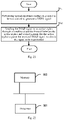
- a sixth embodiment of the present disclosure which however does not form part of the claimed invention, relates to a system for transmitting a signal, as shown in FIG. 24 , including: a touch screen 1101 and an active stylus 1102.
- the touch screen 1101 is configured to perform spread-spectrum coding on a signal to be transmitted to generate a DSSS signal.
- the touch screen 1101 is further configured to send the DSSS signal to the active stylus 1102 through a coupling capacitor 1103 formed between the touch screen 1101 and the active stylus 1102.
- the active stylus 1102 is configured to parse the received DSSS signal to obtain the signal to be transmitted.
- this embodiment is a system embodiment corresponding to the first embodiment, the second embodiment and the third embodiment, and this embodiment may be implemented in cooperation with the first embodiment, the second embodiment and the third embodiment.
- the related technical details as mentioned in the first embodiment, the second embodiment and the third embodiment are still valid in this embodiment, and in order to reduce repetition, no details will be repeated here.
- the related technical details as mentioned in this embodiment may also be applied to the first embodiment, the second embodiment and the third embodiment.
- the DSSS signal is transmitted through the coupling capacitor formed between the active stylus and the touch screen in this embodiment, which can be well applied to DSSS signal transmission in a touch system.
- only one stage of the pre-amplifier circuit, one stage of the hysteresis comparing circuit, and one stage of the digital demodulating circuit are required in the active stylus to implement parsing the received DSSS signal, which renders a simple circuit structure, a small quantity of hardware resources, and relatively low power consumption, and is very applicable to the interactive system of the active stylus and the touch screen that has strict requirements on a circuit size and power consumption, and the like.
- a seventh embodiment of the present disclosure relates to a chip, as shown in FIG. 25 , including: a pre-amplifier circuit 1201, configured to pre-amplify a DSSS signal sent by a touch screen and received through a coupling capacitor formed between an active stylus and the touch screen, and output the pre-amplified DSSS signal to a hysteresis comparing circuit 1202; the hysteresis comparing circuit 1202, configured to restore the pre-amplified DSSS signal to obtain the restored DSSS signal and output the restored DSSS signal to a digital demodulating circuit 1203; and the digital demodulating circuit 1203, configured to demodulate the restored DSSS signal.
- a pre-amplifier circuit 1201 configured to pre-amplify a DSSS signal sent by a touch screen and received through a coupling capacitor formed between an active stylus and the touch screen, and output the pre-amplified DSSS signal to a hysteresis comparing circuit 1202
- the pre-amplifier circuit 1201 may include an inverting amplifier circuit or a non-inverting amplifier circuit
- the hysteresis comparing circuit may include: a non-inverting hysteresis comparing circuit or an inverting hysteresis comparing circuit.
- the inverting amplifier circuit may be a low-impedance inverting amplifier circuit as shown in FIG. 6 .
- the low-impedance inverting amplifier circuit includes: a first operational amplifier, a first feedback resistor RF1 and a first feedback capacitor CF1, where the first operational amplifier has a non-inverting input end connected with an input voltage VCMI, and an inverting input end connected with the DSSS signal.
- the first feedback resistor RF1 is bridged between the inverting input end and an output end of the first operational amplifier, and the first feedback capacitor CF1 is connected in parallel with the first feedback resistor RF1.
- the first feedback resistor RF1 has a first end connected with the inverting input end of the first operational amplifier, and a second end connected with the output end of the first operational amplifier.
- the first feedback capacitor CF1 has a first end connected with the first end of the first feedback resistor RF1, and a second end connected with the second end of the first feedback resistor RF1.
- the non-inverting amplifier circuit may be a high-impedance non-inverting amplifier circuit as shown in FIG. 8 .
- the high-impedance non-inverting amplifier circuit includes: a second operational amplifier, a second feedback resistor RF2, a second feedback capacitor CF2, a first resistor R1 and a second resistor R2, where the second operational amplifier has a non-inverting input end connected with the DSSS signal, and an inverting input end connected with a second end of the second resistor R2, and a first end of the second resistor R2 is connected with a first input voltage VCMI1.
- the second feedback resistor RF2 is bridged between the inverting input end and an output end of the second operational amplifier, and the second feedback capacitor CF2 is connected in parallel with the second feedback resistor RF2. That is to say, the second feedback resistor RF2 has a first end connected with the inverting input end of the second operational amplifier, and a second end connected with the output end of the second operational amplifier.
- the second feedback capacitor CF2 has a first end connected with the first end of the second feedback resistor RF2, and a second end connected with the second end of the second feedback resistor RF2.
- the first resistor R1 has a first end connected with the non-inverting input end of the second operational amplifier, and a second end connected with a second input voltage VCMI2, where VCMI1 and VCMI2 may be the same.
- a circuit diagram of the non-inverting hysteresis comparing circuit may be as shown in FIG. 10 , and includes: a first comparator, a third resistor R3, a fourth resistor R4 and a fifth resistor R5.
- the third resistor R3 has a first end connected with an output end VI of the pre-amplifier circuit, and a second end connected with a non-inverting input end of the first comparator.
- the fourth resistor R4 is bridged between the non-inverting input end and an output end of the first comparator. That is to say, the fourth resistor R4 has a first end connected with the second end of the third resistor R3, and a second end connected with an output end V2 of the first comparator.
- the fifth resistor R5 has a first end connected with an input voltage VCMI, and a second end connected with an inverting input end of the first comparator.
- a circuit diagram of the inverting hysteresis comparing circuit may be as shown in FIG. 12 , and includes: a second comparator, a sixth resistor R6, a seventh resistor R7 and an eighth resistor R8, where the sixth resistor R6 has a first end connected with an input voltage VCMI, and a second end connected with a non-inverting input end of the second comparator.
- the seventh resistor R7 is bridged between the non-inverting input end and an output end of the second comparator. That is to say, the seventh resistor R7 has a first end connected with the second end of the sixth resistor R6, and a second end connected with the output end V2 of the second comparator.
- the eighth resistor R8 has a first end connected with the output end VI of the pre-amplifier circuit, and a second end connected with an inverting input end of the second comparator.
- the DSSS signal is transmitted through the coupling capacitor formed between the active stylus and the touch screen in the embodiment of the present disclosure, which can be well applied to DSSS signal transmission in a touch system.
- only one stage of the pre-amplifier circuit, one stage of the hysteresis comparing circuit, and one stage of the digital demodulating circuit are required to implement parsing the received DSSS signal, which renders a simple circuit structure, a small quantity of hardware resources, and relatively low power consumption, and is very applicable to the interactive system of the active stylus and the touch screen that has strict requirements on a circuit size and power consumption, and the like.
- An eighth embodiment of the present disclosure relates to an active stylus, including the chip according to the seventh embodiment.
- a ninth embodiment of the present disclosure relates to a computer-readable storage medium, storing a computer program.
- the computer program when executed by a processor, performs the above-described method for transmitting a signal embodiment.
- the program may be stored in a storage medium, and include a plurality of instructions so that a device (which may be a single chip microcomputer and a chip, and the like) or a processor executes all or some of the steps of the methods as described in the various embodiments of the present disclosure.
- the foregoing storage medium includes: various media that can store program codes, such as a USB flash disk, a mobile hard disk, a Read-Only Memory (ROM), a Random Access Memory (RAM), a magnetic disk or an optical disk.
Landscapes
- Engineering & Computer Science (AREA)
- General Engineering & Computer Science (AREA)
- Theoretical Computer Science (AREA)
- Human Computer Interaction (AREA)
- Physics & Mathematics (AREA)
- General Physics & Mathematics (AREA)
- Position Input By Displaying (AREA)
- Circuits Of Receivers In General (AREA)
Claims (15)
- Verfahren zur Signalübertragung, das von einem aktiven Eingabestift (101) angewandt wird und Folgendes umfasst:Empfangen (201), durch eine Elektrode (102, 302, 303) in dem aktiven Eingabestift (101), eines Direct Sequence Spread Spectrum, DSSS, Signals, wobei das DSSS-Signal von einem berührungsempfindlichen Bildschirm (104) über einen Kopplungskondensator (103, 305, 306, 501) gesendet wird, der zwischen der Elektrode (102, 302, 303) und dem berührungsempfindlichen Bildschirm (104) gebildet ist,Vorverstärken (601) des empfangenen DSSS-Signals durch eine Vorverstärkerschaltung (503) in dem aktiven Eingabestift (101);Eingeben (602), durch die Vorverstärkerschaltung (503), des vorverstärkten DSSS-Signals in eine Hysterese-Vergleichsschaltung (504), wobei die Hysterese-Vergleichsschaltung (504) eine Komparatorschaltung mit Hysterese ist;Wiederherstellen (602), durch die Hysterese-Vergleichsschaltung (504), des vorverstärkten DSSS-Signals, um ein wiederhergestelltes DSSS-Signal gemäß dem ursprünglich gesendeten DSSS-Signal zu erhalten;Eingeben (603), durch die Hysterese-Vergleichsschaltung (504), des wiederhergestellten DSSS-Signals in eine digitale Demodulationsschaltung (505);Demodulieren (603), durch die digitale Demodulationsschaltung (505), des wiederhergestellten DSSS-Signals, um ein ursprüngliches Signal zu erhalten, das nicht spreizspektrumcodiert ist; undAusgeben (603) des ursprünglichen Signals durch die digitale Demodulationsschaltung (505).
- Verfahren zur Signalübertragung nach Anspruch 1, wobei das Demodulieren des wiederhergestellten DSSS-Signals durch die digitale Demodulationsschaltung (505) Folgendes umfasst:Abtasten (701) des wiederhergestellten DSSS-Signals durch die digitale Demodulationsschaltung (505), um ein ursprüngliches codiertes Signal zu erhalten;Durchführen (702) einer bitweisen XOR-Operation auf dem ursprünglichen codierten Signal und einem voreingestellten demodulierten Autokorrelationssignal;Kumulieren (703) eines Ergebnisses der bitweisen XOR-Operation, um ein Kumulationsergebnis zu erhalten; undDemodulieren (704) des wiederhergestellten DSSS-Signals gemäß dem Kumulationsergebnis.
- Verfahren zur Signalübertragung nach Anspruch 2, wobei das Durchführen der bitweisen XOR-Operation auf dem ursprünglichen codierten Signal und dem voreingestellten demodulierten Autokorrelationssignal Folgendes umfasst:Verschieben des demodulierten Autokorrelationssignals als Ganzes um 1 Bit nach hinten, nachdem alle B Bits des ursprünglichen codierten Signals gesammelt wurden, wobei B die Anzahl der Bits des demodulierten Autokorrelationssignals ist; wobei jedes Bit N Abtastpunkte umfasst, und das Verschieben wiederholt wird, während jeder Abtastpunkt gesammelt wird;Durchführen der bitweisen XOR-Operation auf den gesammelten B Bits des ursprünglichen codierten Signals und des demodulierten B-Bit-Autokorrelationssignals;Kumulieren des Ergebnisses der bitweisen XOR-Operation der gesammelten B Bits des ursprünglichen codierten Signals und des demodulierten B-Bit-Autokorrelationssignals, um das Kumulationsergebnis zu erhalten;Demodulieren des wiederhergestellten DSSS-Signals gemäß einem Vergleichsergebnis zwischen dem Kumulationsergebnis und einem voreingestellten Schwellenwert.
- Verfahren zur Signalübertragung nach Anspruch 3, wobei das ursprüngliche codierte Signal ein Signal von einem ersten Typ, ein Signal von einem zweiten Typ und ein Signal von einem dritten Typ umfasst, wobei das Signal vom ersten Typ ein Spreizspektrumcode ist, der "0" in dem ursprüngliche Signal entspricht, das Signal vom zweiten Typ ein Spreizspektrumcode ist, der "1" in dem ursprünglichen Signal entspricht und das Signal vom dritten Typ ein unerwünschtes Signal ist;wenn festgestellt wird, dass das Kumulationsergebnis kleiner oder gleich einem ersten voreingestellten Schwellenwert ist, Identifizieren der gesammelten B Bits des ursprünglichen codierten Signals als das Signal vom ersten Typ;wenn festgestellt wird, dass das Kumulationsergebnis größer oder gleich einem zweiten voreingestellten Schwellenwert ist, Identifizieren der gesammelten B Bits des ursprünglichen codierten Signals als das Signal vom zweiten Typ, wobei der zweite voreingestellte Schwellenwert größer als der erste voreingestellte Schwellenwert ist;wenn festgestellt wird, dass das Kumulationsergebnis größer als der erste voreingestellte Schwellenwert und kleiner als der zweite voreingestellten Schwellenwert ist, Identifizieren der gesammelten B Bits des ursprünglichen codierten Signals als das unerwünschte Signal.
- Verfahren zur Signalübertragung nach Anspruch 4, wobei, wenn festgestellt wird, dass das Kumulationsergebnis kleiner oder gleich dem ersten voreingestellten Schwellenwert ist, das Verfahren ferner Folgendes umfasst: Verwenden eines Zeitpunkts, an dem die gesammelten B Bits des ursprünglichen codierten Signals beginnen, als ein Zeitpunkt, an dem das identifizierte Signal vom ersten Typ beginnt;
wenn festgestellt wird, dass das Kumulationsergebnis größer oder gleich dem zweiten voreingestellten Schwellenwert ist, das Verfahren ferner Folgendes umfasst: Verwenden eines Zeitpunkts, an dem die gesammelten B Bits des ursprünglichen codierten Signals beginnen, als ein Zeitpunkt, an dem das identifizierte Signal vom zweiten Typ beginnt. - Verfahren zur Signalübertragung nach Anspruch 4, wobei der erste voreingestellte Schwellenwert größer oder gleich 0 und kleiner oder gleich B*N/2 ist, wobei der zweite voreingestellte Schwellenwert größer als B*N/2 und kleiner oder gleich B*N ist, wobei N eine Abtastfrequenz ist, mit der die digitale Demodulationsschaltung das wiederhergestellte DSSS-Signal abtastet.
- Verfahren zur Signalübertragung nach einem der Ansprüche 1 bis 6, wobei die Vorverstärkerschaltung Folgendes umfasst: eine nichtinvertierende Verstärkerschaltung oder eine invertierende Verstärkerschaltung (5031, 5032).
- Verfahren zur Signalübertragung nach einem der Ansprüche 1 bis 7, wobei die Hysterese-Vergleichsschaltung Folgendes umfasst: eine nichtinvertierende Hysterese-Vergleichsschaltung oder eine invertierende Hysterese-Vergleichsschaltung (5041, 5042).
- Verfahren zur Signalübertragung nach einem der Ansprüche 1 bis 8, wobei der aktive Eingabestift eine Hauptelektrode und eine Nebenelektrode umfasst, und der Kopplungskondensator, der zwischen dem aktiven Eingabestift und dem berührungsempfindlichen Bildschirm gebildet ist, Folgendes umfasst:
einen Kopplungskondensator, der zwischen der Hauptelektrode und dem berührungsempfindlichen Bildschirm gebildet ist, oder einen Kopplungskondensator, der zwischen der Nebenelektrode und dem berührungsempfindlichen Bildschirm gebildet ist. - Chip, der eine Vorverstärkerschaltung (503), eine Hysterese-Vergleichsschaltung und eine digitale Demodulationsschaltung (505) umfasst;wobei die Vorverstärkerschaltung (503) dazu ausgestaltet ist, ein Direct Sequence Spread Spectrum, DSSS, Signal, das durch einen berührungsempfindlichen Bildschirm (104) über einen Kopplungskondensator (103, 305, 306, 501) gesendet wird, der zwischen einer Elektrode (102, 302, 303) in einem aktiven Eingabestift (101) und dem berührungsempfindlichen Bildschirm (104) gebildet ist, vorzuverstärken, wobei das DSSS-Signal vorverstärkt wird, wenn es durch den aktiven Eingabestift (101) empfangen wird, und die Vorverstärkerschaltung (503) ferner dazu ausgestaltet ist, das vorverstärkte DSSS-Signal an die Hysterese-Vergleichsschaltung (504) auszugeben, wobei die Hysterese-Vergleichsschaltung (504) eine Komparatorschaltung mit Hysterese ist;die Hysterese-Vergleichsschaltung (504) dazu ausgestaltet ist, das vorverstärkte DSSS-Signal wiederherzustellen, um ein wiederhergestelltes DSSS-Signal gemäß dem ursprünglich gesendeten DSSS-Signal zu erhalten und das wiederhergestellte DSSS-Signal an die digitale Demodulationsschaltung (505) auszugeben;die digitale Demodulationsschaltung (505) dazu ausgestaltet ist, das wiederhergestellte DSSS-Signal zu demodulieren, um ein ursprüngliches Signal zu erhalten, das nicht spreizspektrumcodiert ist, und das ursprüngliche Signal auszugeben.
- Chip nach Anspruch 10, wobei die digitale Demodulationsschaltung (505) für Folgendes ausgestaltet ist:Abtasten des wiederhergestellten DSSS-Signals durch die digitale Demodulationsschaltung (505), um ein ursprüngliches codiertes Signal zu erhalten;Durchführen einer bitweisen XOR-Operation auf dem ursprünglichen codierten Signal und einem voreingestellten demodulierten Autokorrelationssignal;Kumulieren eines Ergebnisses der bitweisen XOR-Operation, um ein Kumulationsergebnis zu erhalten; undDemodulieren des wiederhergestellten DSSS-Signals gemäß dem Kumulationsergebnis.
- Chip nach Anspruch 11, wobei die digitale Demodulationsschaltung (505) für Folgendes ausgestaltet ist:Verschieben des demodulierten Autokorrelationssignals als Ganzes um 1 Bit nach hinten, nachdem alle B Bits des ursprünglichen codierten Signals gesammelt wurden, wobei B die Anzahl der Bits des demodulierten Autokorrelationssignals ist; wobei jedes Bit N Abtastpunkte umfasst, und das Verschieben wiederholt wird, während jeder Abtastpunkt gesammelt wird;Durchführen der bitweisen XOR-Operation auf den gesammelten B Bits des ursprünglichen codierten Signals und des demodulierten B-Bit-Autokorrelationssignals;Kumulieren des Ergebnisses der bitweisen XOR-Operation der gesammelten B Bits des ursprünglichen codierten Signals und des demodulierten B-Bit-Autokorrelationssignals, um das Kumulationsergebnis zu erhalten;Demodulieren des wiederhergestellten DSSS-Signals gemäß einem Vergleichsergebnis zwischen dem Kumulationsergebnis und einem voreingestellten Schwellenwert.
- Chip nach einem der Ansprüche 10 bis 12, wobei die Vorverstärkerschaltung Folgendes umfasst: eine invertierende Verstärkerschaltung (5031, 5032) oder eine nicht invertierende Verstärkerschaltung;wobei die invertierende Verstärkerschaltung (5031, 5032) eine invertierende Verstärkerschaltung mit niedriger Impedanz umfasst und die invertierende Verstärkerschaltung mit niedriger Impedanz Folgendes umfasst: einen ersten Operationsverstärker, einen ersten Rückkopplungswiderstand und einen ersten Rückkopplungskondensator, wobei der erste Operationsverstärker ein erstes nichtinvertierendes Eingangsende, das mit einer Eingangsspannung verbunden ist, und ein invertierendes Eingangsende aufweist, das mit dem DSSS-Signal verbunden ist; der erste Rückkopplungswiderstand zwischen dem invertierenden Eingangsende und einem Ausgangsende des ersten Operationsverstärkers überbrückt ist und der erste Rückkopplungskondensator mit dem ersten Rückkopplungswiderstand parallel geschaltet ist; oderwobei die nichtinvertierende Verstärkerschaltung eine nichtinvertierende Verstärkerschaltung mit hoher Impedanz umfasst und die nichtinvertierende Verstärkerschaltung mit hoher Impedanz Folgendes umfasst: einen zweiten Operationsverstärker, einen zweiten Rückkopplungswiderstand, einen zweiten Rückkopplungskondensator, einen ersten Widerstand und einen zweiten Widerstand, wobei der zweite Operationsverstärker ein nichtinvertierendes Eingangsende, das mit dem DSSS-Signal verbunden ist, und ein invertierendes Eingangsende aufweist, das mit einem zweiten Ende des zweiten Widerstands verbunden ist, und ein erstes Ende des zweiten Widerstands mit einer ersten Eingangsspannung verbunden ist; der zweite Rückkopplungswiderstand zwischen dem invertierenden Eingangsende und einem Ausgangsende des zweiten Operationsverstärkers überbrückt ist; der zweite Rückkopplungskondensator mit dem zweiten Rückkopplungswiederstand parallel geschaltet ist und der erste Widerstand ein erstes Ende, das mit dem nichtinvertierenden Eingangsende des zweiten Operationsverstärkers verbunden ist, und ein zweites Ende aufweist, das mit einer zweiten Eingangsspannung verbunden ist.
- Chip nach einem der Ansprüche 10 bis 13, wobei die Hysterese-Vergleichsschaltung eine nichtinvertierende Hysterese-Vergleichsschaltung oder eine invertierende Hysterese-Vergleichsschaltung (5041, 5042) umfasst;die nichtinvertierende Hysterese-Vergleichsschaltung Folgendes umfasst: einen ersten Komparator, einen dritten Widerstand, einen vierten Widerstand und einen fünften Widerstand, wobei der dritte Widerstand ein erstes Ende, das mit einem Ausgangsende der Vorverstärkerschaltung verbunden ist, und ein zweites Ende aufweist, das mit einem nichtinvertierenden Eingangsende des ersten Komparators verbunden ist, wobei der vierte Widerstand zwischen dem nichtinvertierenden Eingangsende und einem Ausgangsende des ersten Komparators überbrückt ist und der fünfte Widerstand ein erstes Ende, das mit einer Eingangsspannung verbunden ist, und ein zweites Ende aufweist, das mit einem invertierenden Eingangsende des ersten Komparators verbunden ist; oderdie invertierende Hysterese-Vergleichsschaltung (5041, 5042) Folgendes umfasst: einen zweiten Komparator, einen sechsten Widerstand, einen siebten Widerstand und einen achten Widerstand; wobei der sechste Widerstand ein erstes Ende, das mit einer Eingangsspannung verbunden ist, und ein zweites Ende aufweist, das mit einem nichtinvertierenden Eingangsende des zweiten Komparators verbunden ist, wobei der siebte Widerstand zwischen dem nichtinvertierenden Eingangsende und einem Ausgangsende des zweiten Komparators überbrückt ist, der achte Widerstand ein erstes Ende, das mit dem Ausgangsende der Vorverstärkerschaltung verbunden ist, und ein zweites Ende aufweist, das mit einem invertierenden Eingangsende des zweiten Komparators verbunden ist.
- Aktiver Eingabestift, der Folgendes umfasst:
den Chip nach einem der Ansprüche 10 bis 14.
Applications Claiming Priority (1)
| Application Number | Priority Date | Filing Date | Title |
|---|---|---|---|
| PCT/CN2019/079550 WO2020191585A1 (zh) | 2019-03-25 | 2019-03-25 | 信号传输方法、系统、主动笔、触控屏和可读存储介质 |
Publications (3)
| Publication Number | Publication Date |
|---|---|
| EP3764203A1 EP3764203A1 (de) | 2021-01-13 |
| EP3764203A4 EP3764203A4 (de) | 2021-05-12 |
| EP3764203B1 true EP3764203B1 (de) | 2022-11-16 |
Family
ID=72608748
Family Applications (1)
| Application Number | Title | Priority Date | Filing Date |
|---|---|---|---|
| EP19920633.5A Active EP3764203B1 (de) | 2019-03-25 | 2019-03-25 | Signalübertragungsverfahren und -system, aktiver eingabestift, berührungsbildschirm und lesbares speichermedium |
Country Status (4)
| Country | Link |
|---|---|
| US (1) | US11106318B2 (de) |
| EP (1) | EP3764203B1 (de) |
| CN (1) | CN112074803A (de) |
| WO (1) | WO2020191585A1 (de) |
Families Citing this family (2)
| Publication number | Priority date | Publication date | Assignee | Title |
|---|---|---|---|---|
| WO2022165839A1 (zh) * | 2021-02-08 | 2022-08-11 | 深圳市汇顶科技股份有限公司 | 抗干扰的方法、触控芯片及主动笔芯片 |
| CN116048289B (zh) * | 2022-08-25 | 2024-08-06 | 荣耀终端有限公司 | 手写笔的出水控制方法及电子设备 |
Family Cites Families (10)
| Publication number | Priority date | Publication date | Assignee | Title |
|---|---|---|---|---|
| CN203084673U (zh) * | 2013-01-23 | 2013-07-24 | 成都有形科技有限公司 | 主动式电容笔 |
| US11392221B2 (en) * | 2013-11-08 | 2022-07-19 | Egalax_Empia Technology Inc. | Touch sensitive processing apparatus, system and operating method thereof for receiving electrical signals carrying pressure information |
| CN103941889B (zh) * | 2014-03-17 | 2017-07-18 | 汉王科技股份有限公司 | 电容笔、电容触控面板和触控装置 |
| CN105468170B (zh) * | 2014-08-13 | 2018-09-11 | 比亚迪股份有限公司 | 电容笔与触摸屏之间的数据传输方法、系统和装置 |
| JP6445883B2 (ja) * | 2015-01-30 | 2018-12-26 | 東芝メモリ株式会社 | 受信回路及び通信システム |
| TWI563418B (en) * | 2015-10-16 | 2016-12-21 | Waltop Int Corp | Signal decoding and modulation processing system for capacitive stylus |
| KR102520695B1 (ko) * | 2015-12-31 | 2023-04-13 | 엘지디스플레이 주식회사 | 능동형 스타일러스 펜과 그를 포함한 터치 센싱 시스템, 및 그 구동방법 |
| US10324547B2 (en) * | 2015-12-31 | 2019-06-18 | Lg Display Co., Ltd. | Active stylus pen, touch sensing system and driving method thereof |
| WO2018035843A1 (zh) * | 2016-08-26 | 2018-03-01 | 深圳市汇顶科技股份有限公司 | 信号发射方法、信号解析方法、主动笔及触控屏 |
| CN109521893B (zh) * | 2018-10-17 | 2022-11-25 | 京东方科技集团股份有限公司 | 触控笔、触控面板、触控感测系统及其控制方法 |
-
2019
- 2019-03-25 CN CN201980000474.7A patent/CN112074803A/zh active Pending
- 2019-03-25 WO PCT/CN2019/079550 patent/WO2020191585A1/zh not_active Ceased
- 2019-03-25 EP EP19920633.5A patent/EP3764203B1/de active Active
-
2020
- 2020-09-29 US US17/037,531 patent/US11106318B2/en not_active Expired - Fee Related
Also Published As
| Publication number | Publication date |
|---|---|
| US11106318B2 (en) | 2021-08-31 |
| CN112074803A (zh) | 2020-12-11 |
| EP3764203A1 (de) | 2021-01-13 |
| EP3764203A4 (de) | 2021-05-12 |
| WO2020191585A1 (zh) | 2020-10-01 |
| US20210011579A1 (en) | 2021-01-14 |
Similar Documents
| Publication | Publication Date | Title |
|---|---|---|
| US20100322294A1 (en) | Human body communication device, human body communication system and method using the same | |
| CN109564476B (zh) | 模拟电路、位置指示器及系统 | |
| CN103312419A (zh) | 基于音频或超声波的数据通讯方法和系统 | |
| WO2023065886A1 (zh) | 唤醒方法、装置及电子设备 | |
| US11106318B2 (en) | Method and system for transmitting signal, active stylus, touch screen and readable storage medium | |
| US12073033B2 (en) | System and sensor controller for use with active pen | |
| WO2014170181A1 (en) | Host communication circuit, client communication circuit, communication system and communication method | |
| EP3816807A1 (de) | Serielles kommunikationsgerät und serielles kommunikationsverfahren | |
| US20180188853A1 (en) | Touch sensing system and data transmission method of a touch panel | |
| US20010046241A1 (en) | Synchronization correction circuit | |
| JP6580346B2 (ja) | 送信装置、受信装置および送受信システム | |
| CN102769494A (zh) | 一种数据发送、接收方法及发送、接收装置 | |
| CN117938600A (zh) | Fsk解调器、fsk解调方法和无线充电接收装置 | |
| CN111665756A (zh) | 基于fpga实现非同步信号采样的方法、装置、电子设备及可读存储介质 | |
| KR101476908B1 (ko) | 송신장치 및 모바일의 이어폰 포트를 이용한 통신 시스템 | |
| CN103490829A (zh) | 一种防止射频信号干扰的方法和装置 | |
| CN115134272B (zh) | 时延确定方法、装置、计算机设备和存储介质 | |
| EP2068518A1 (de) | Signalempfängervorrichtung und signalform-formungsverfahren | |
| CN111404561B (zh) | 基于资源块分推的信号发射方法及相关产品 | |
| CN107122325B (zh) | 基于通用串行总线的数据传输系统及方法 | |
| CN103685903B (zh) | 摄像机姿态数据传输装置及其传输方法 | |
| Wang et al. | A body channel communication transceiver system utilizing manchester code for wban with multi-sensor nodes | |
| CN119759836B (zh) | 毫米波芯片的级联处理方法、数据传输接口、设备、介质 | |
| KR102836555B1 (ko) | 구축함 전투체계 다기능 위상배열레이다에서의 참조 클럭 기반의 직렬화-병렬화 인터페이스 시스템 및 이의 동작 방법 | |
| CN103491235B (zh) | 一种数据传输方法及终端 |
Legal Events
| Date | Code | Title | Description |
|---|---|---|---|
| STAA | Information on the status of an ep patent application or granted ep patent |
Free format text: STATUS: UNKNOWN |
|
| STAA | Information on the status of an ep patent application or granted ep patent |
Free format text: STATUS: THE INTERNATIONAL PUBLICATION HAS BEEN MADE |
|
| PUAI | Public reference made under article 153(3) epc to a published international application that has entered the european phase |
Free format text: ORIGINAL CODE: 0009012 |
|
| STAA | Information on the status of an ep patent application or granted ep patent |
Free format text: STATUS: REQUEST FOR EXAMINATION WAS MADE |
|
| 17P | Request for examination filed |
Effective date: 20200929 |
|
| AK | Designated contracting states |
Kind code of ref document: A1 Designated state(s): AL AT BE BG CH CY CZ DE DK EE ES FI FR GB GR HR HU IE IS IT LI LT LU LV MC MK MT NL NO PL PT RO RS SE SI SK SM TR |
|
| AX | Request for extension of the european patent |
Extension state: BA ME |
|
| A4 | Supplementary search report drawn up and despatched |
Effective date: 20210412 |
|
| RIC1 | Information provided on ipc code assigned before grant |
Ipc: G06F 3/0354 20130101AFI20210406BHEP Ipc: G06F 3/038 20130101ALI20210406BHEP Ipc: G06F 3/044 20060101ALI20210406BHEP |
|
| STAA | Information on the status of an ep patent application or granted ep patent |
Free format text: STATUS: EXAMINATION IS IN PROGRESS |
|
| 17Q | First examination report despatched |
Effective date: 20220121 |
|
| DAV | Request for validation of the european patent (deleted) | ||
| DAX | Request for extension of the european patent (deleted) | ||
| GRAP | Despatch of communication of intention to grant a patent |
Free format text: ORIGINAL CODE: EPIDOSNIGR1 |
|
| STAA | Information on the status of an ep patent application or granted ep patent |
Free format text: STATUS: GRANT OF PATENT IS INTENDED |
|
| RIC1 | Information provided on ipc code assigned before grant |
Ipc: G06F 3/041 20060101ALI20220802BHEP Ipc: G06F 3/044 20060101ALI20220802BHEP Ipc: G06F 3/038 20130101ALI20220802BHEP Ipc: G06F 3/0354 20130101AFI20220802BHEP |
|
| INTG | Intention to grant announced |
Effective date: 20220822 |
|
| GRAS | Grant fee paid |
Free format text: ORIGINAL CODE: EPIDOSNIGR3 |
|
| GRAA | (expected) grant |
Free format text: ORIGINAL CODE: 0009210 |
|
| STAA | Information on the status of an ep patent application or granted ep patent |
Free format text: STATUS: THE PATENT HAS BEEN GRANTED |
|
| AK | Designated contracting states |
Kind code of ref document: B1 Designated state(s): AL AT BE BG CH CY CZ DE DK EE ES FI FR GB GR HR HU IE IS IT LI LT LU LV MC MK MT NL NO PL PT RO RS SE SI SK SM TR |
|
| REG | Reference to a national code |
Ref country code: GB Ref legal event code: FG4D |
|
| REG | Reference to a national code |
Ref country code: CH Ref legal event code: EP |
|
| REG | Reference to a national code |
Ref country code: DE Ref legal event code: R096 Ref document number: 602019022104 Country of ref document: DE |
|
| REG | Reference to a national code |
Ref country code: IE Ref legal event code: FG4D |
|
| REG | Reference to a national code |
Ref country code: AT Ref legal event code: REF Ref document number: 1532164 Country of ref document: AT Kind code of ref document: T Effective date: 20221215 |
|
| REG | Reference to a national code |
Ref country code: LT Ref legal event code: MG9D |
|
| REG | Reference to a national code |
Ref country code: NL Ref legal event code: MP Effective date: 20221116 |
|
| REG | Reference to a national code |
Ref country code: AT Ref legal event code: MK05 Ref document number: 1532164 Country of ref document: AT Kind code of ref document: T Effective date: 20221116 |
|
| PG25 | Lapsed in a contracting state [announced via postgrant information from national office to epo] |
Ref country code: SE Free format text: LAPSE BECAUSE OF FAILURE TO SUBMIT A TRANSLATION OF THE DESCRIPTION OR TO PAY THE FEE WITHIN THE PRESCRIBED TIME-LIMIT Effective date: 20221116 Ref country code: PT Free format text: LAPSE BECAUSE OF FAILURE TO SUBMIT A TRANSLATION OF THE DESCRIPTION OR TO PAY THE FEE WITHIN THE PRESCRIBED TIME-LIMIT Effective date: 20230316 Ref country code: NO Free format text: LAPSE BECAUSE OF FAILURE TO SUBMIT A TRANSLATION OF THE DESCRIPTION OR TO PAY THE FEE WITHIN THE PRESCRIBED TIME-LIMIT Effective date: 20230216 Ref country code: LT Free format text: LAPSE BECAUSE OF FAILURE TO SUBMIT A TRANSLATION OF THE DESCRIPTION OR TO PAY THE FEE WITHIN THE PRESCRIBED TIME-LIMIT Effective date: 20221116 Ref country code: FI Free format text: LAPSE BECAUSE OF FAILURE TO SUBMIT A TRANSLATION OF THE DESCRIPTION OR TO PAY THE FEE WITHIN THE PRESCRIBED TIME-LIMIT Effective date: 20221116 Ref country code: ES Free format text: LAPSE BECAUSE OF FAILURE TO SUBMIT A TRANSLATION OF THE DESCRIPTION OR TO PAY THE FEE WITHIN THE PRESCRIBED TIME-LIMIT Effective date: 20221116 Ref country code: AT Free format text: LAPSE BECAUSE OF FAILURE TO SUBMIT A TRANSLATION OF THE DESCRIPTION OR TO PAY THE FEE WITHIN THE PRESCRIBED TIME-LIMIT Effective date: 20221116 |
|
| PG25 | Lapsed in a contracting state [announced via postgrant information from national office to epo] |
Ref country code: RS Free format text: LAPSE BECAUSE OF FAILURE TO SUBMIT A TRANSLATION OF THE DESCRIPTION OR TO PAY THE FEE WITHIN THE PRESCRIBED TIME-LIMIT Effective date: 20221116 Ref country code: PL Free format text: LAPSE BECAUSE OF FAILURE TO SUBMIT A TRANSLATION OF THE DESCRIPTION OR TO PAY THE FEE WITHIN THE PRESCRIBED TIME-LIMIT Effective date: 20221116 Ref country code: LV Free format text: LAPSE BECAUSE OF FAILURE TO SUBMIT A TRANSLATION OF THE DESCRIPTION OR TO PAY THE FEE WITHIN THE PRESCRIBED TIME-LIMIT Effective date: 20221116 Ref country code: IS Free format text: LAPSE BECAUSE OF FAILURE TO SUBMIT A TRANSLATION OF THE DESCRIPTION OR TO PAY THE FEE WITHIN THE PRESCRIBED TIME-LIMIT Effective date: 20230316 Ref country code: HR Free format text: LAPSE BECAUSE OF FAILURE TO SUBMIT A TRANSLATION OF THE DESCRIPTION OR TO PAY THE FEE WITHIN THE PRESCRIBED TIME-LIMIT Effective date: 20221116 Ref country code: GR Free format text: LAPSE BECAUSE OF FAILURE TO SUBMIT A TRANSLATION OF THE DESCRIPTION OR TO PAY THE FEE WITHIN THE PRESCRIBED TIME-LIMIT Effective date: 20230217 |
|
| PGFP | Annual fee paid to national office [announced via postgrant information from national office to epo] |
Ref country code: GB Payment date: 20230322 Year of fee payment: 5 Ref country code: DE Payment date: 20230321 Year of fee payment: 5 |
|
| PG25 | Lapsed in a contracting state [announced via postgrant information from national office to epo] |
Ref country code: NL Free format text: LAPSE BECAUSE OF FAILURE TO SUBMIT A TRANSLATION OF THE DESCRIPTION OR TO PAY THE FEE WITHIN THE PRESCRIBED TIME-LIMIT Effective date: 20221116 |
|
| PG25 | Lapsed in a contracting state [announced via postgrant information from national office to epo] |
Ref country code: SM Free format text: LAPSE BECAUSE OF FAILURE TO SUBMIT A TRANSLATION OF THE DESCRIPTION OR TO PAY THE FEE WITHIN THE PRESCRIBED TIME-LIMIT Effective date: 20221116 Ref country code: RO Free format text: LAPSE BECAUSE OF FAILURE TO SUBMIT A TRANSLATION OF THE DESCRIPTION OR TO PAY THE FEE WITHIN THE PRESCRIBED TIME-LIMIT Effective date: 20221116 Ref country code: EE Free format text: LAPSE BECAUSE OF FAILURE TO SUBMIT A TRANSLATION OF THE DESCRIPTION OR TO PAY THE FEE WITHIN THE PRESCRIBED TIME-LIMIT Effective date: 20221116 Ref country code: DK Free format text: LAPSE BECAUSE OF FAILURE TO SUBMIT A TRANSLATION OF THE DESCRIPTION OR TO PAY THE FEE WITHIN THE PRESCRIBED TIME-LIMIT Effective date: 20221116 Ref country code: CZ Free format text: LAPSE BECAUSE OF FAILURE TO SUBMIT A TRANSLATION OF THE DESCRIPTION OR TO PAY THE FEE WITHIN THE PRESCRIBED TIME-LIMIT Effective date: 20221116 |
|
| REG | Reference to a national code |
Ref country code: DE Ref legal event code: R097 Ref document number: 602019022104 Country of ref document: DE |
|
| PG25 | Lapsed in a contracting state [announced via postgrant information from national office to epo] |
Ref country code: SK Free format text: LAPSE BECAUSE OF FAILURE TO SUBMIT A TRANSLATION OF THE DESCRIPTION OR TO PAY THE FEE WITHIN THE PRESCRIBED TIME-LIMIT Effective date: 20221116 Ref country code: AL Free format text: LAPSE BECAUSE OF FAILURE TO SUBMIT A TRANSLATION OF THE DESCRIPTION OR TO PAY THE FEE WITHIN THE PRESCRIBED TIME-LIMIT Effective date: 20221116 |
|
| PLBE | No opposition filed within time limit |
Free format text: ORIGINAL CODE: 0009261 |
|
| STAA | Information on the status of an ep patent application or granted ep patent |
Free format text: STATUS: NO OPPOSITION FILED WITHIN TIME LIMIT |
|
| 26N | No opposition filed |
Effective date: 20230817 |
|
| PG25 | Lapsed in a contracting state [announced via postgrant information from national office to epo] |
Ref country code: MC Free format text: LAPSE BECAUSE OF FAILURE TO SUBMIT A TRANSLATION OF THE DESCRIPTION OR TO PAY THE FEE WITHIN THE PRESCRIBED TIME-LIMIT Effective date: 20221116 |
|
| REG | Reference to a national code |
Ref country code: CH Ref legal event code: PL |
|
| PG25 | Lapsed in a contracting state [announced via postgrant information from national office to epo] |
Ref country code: SI Free format text: LAPSE BECAUSE OF FAILURE TO SUBMIT A TRANSLATION OF THE DESCRIPTION OR TO PAY THE FEE WITHIN THE PRESCRIBED TIME-LIMIT Effective date: 20221116 |
|
| REG | Reference to a national code |
Ref country code: BE Ref legal event code: MM Effective date: 20230331 |
|
| PG25 | Lapsed in a contracting state [announced via postgrant information from national office to epo] |
Ref country code: LU Free format text: LAPSE BECAUSE OF NON-PAYMENT OF DUE FEES Effective date: 20230325 |
|
| REG | Reference to a national code |
Ref country code: IE Ref legal event code: MM4A |
|
| PG25 | Lapsed in a contracting state [announced via postgrant information from national office to epo] |
Ref country code: LI Free format text: LAPSE BECAUSE OF NON-PAYMENT OF DUE FEES Effective date: 20230331 Ref country code: IE Free format text: LAPSE BECAUSE OF NON-PAYMENT OF DUE FEES Effective date: 20230325 Ref country code: FR Free format text: LAPSE BECAUSE OF NON-PAYMENT OF DUE FEES Effective date: 20230331 Ref country code: CH Free format text: LAPSE BECAUSE OF NON-PAYMENT OF DUE FEES Effective date: 20230331 |
|
| PG25 | Lapsed in a contracting state [announced via postgrant information from national office to epo] |
Ref country code: BE Free format text: LAPSE BECAUSE OF NON-PAYMENT OF DUE FEES Effective date: 20230331 |
|
| PG25 | Lapsed in a contracting state [announced via postgrant information from national office to epo] |
Ref country code: IT Free format text: LAPSE BECAUSE OF FAILURE TO SUBMIT A TRANSLATION OF THE DESCRIPTION OR TO PAY THE FEE WITHIN THE PRESCRIBED TIME-LIMIT Effective date: 20221116 |
|
| REG | Reference to a national code |
Ref country code: DE Ref legal event code: R119 Ref document number: 602019022104 Country of ref document: DE |
|
| PG25 | Lapsed in a contracting state [announced via postgrant information from national office to epo] |
Ref country code: BG Free format text: LAPSE BECAUSE OF FAILURE TO SUBMIT A TRANSLATION OF THE DESCRIPTION OR TO PAY THE FEE WITHIN THE PRESCRIBED TIME-LIMIT Effective date: 20221116 |
|
| GBPC | Gb: european patent ceased through non-payment of renewal fee |
Effective date: 20240325 |
|
| PG25 | Lapsed in a contracting state [announced via postgrant information from national office to epo] |
Ref country code: BG Free format text: LAPSE BECAUSE OF FAILURE TO SUBMIT A TRANSLATION OF THE DESCRIPTION OR TO PAY THE FEE WITHIN THE PRESCRIBED TIME-LIMIT Effective date: 20221116 |
|
| PG25 | Lapsed in a contracting state [announced via postgrant information from national office to epo] |
Ref country code: DE Free format text: LAPSE BECAUSE OF NON-PAYMENT OF DUE FEES Effective date: 20241001 |
|
| PG25 | Lapsed in a contracting state [announced via postgrant information from national office to epo] |
Ref country code: GB Free format text: LAPSE BECAUSE OF NON-PAYMENT OF DUE FEES Effective date: 20240325 |
|
| PG25 | Lapsed in a contracting state [announced via postgrant information from national office to epo] |
Ref country code: GB Free format text: LAPSE BECAUSE OF NON-PAYMENT OF DUE FEES Effective date: 20240325 Ref country code: DE Free format text: LAPSE BECAUSE OF NON-PAYMENT OF DUE FEES Effective date: 20241001 |
|
| PG25 | Lapsed in a contracting state [announced via postgrant information from national office to epo] |
Ref country code: CY Free format text: LAPSE BECAUSE OF FAILURE TO SUBMIT A TRANSLATION OF THE DESCRIPTION OR TO PAY THE FEE WITHIN THE PRESCRIBED TIME-LIMIT; INVALID AB INITIO Effective date: 20190325 |
|
| PG25 | Lapsed in a contracting state [announced via postgrant information from national office to epo] |
Ref country code: HU Free format text: LAPSE BECAUSE OF FAILURE TO SUBMIT A TRANSLATION OF THE DESCRIPTION OR TO PAY THE FEE WITHIN THE PRESCRIBED TIME-LIMIT; INVALID AB INITIO Effective date: 20190325 |
|
| PG25 | Lapsed in a contracting state [announced via postgrant information from national office to epo] |
Ref country code: TR Free format text: LAPSE BECAUSE OF FAILURE TO SUBMIT A TRANSLATION OF THE DESCRIPTION OR TO PAY THE FEE WITHIN THE PRESCRIBED TIME-LIMIT Effective date: 20221116 |