EP3763851A1 - Plating film and plated member - Google Patents
Plating film and plated member Download PDFInfo
- Publication number
- EP3763851A1 EP3763851A1 EP19764913.0A EP19764913A EP3763851A1 EP 3763851 A1 EP3763851 A1 EP 3763851A1 EP 19764913 A EP19764913 A EP 19764913A EP 3763851 A1 EP3763851 A1 EP 3763851A1
- Authority
- EP
- European Patent Office
- Prior art keywords
- plating film
- plating
- plated member
- electrically conductive
- film
- Prior art date
- Legal status (The legal status is an assumption and is not a legal conclusion. Google has not performed a legal analysis and makes no representation as to the accuracy of the status listed.)
- Pending
Links
Images

Classifications
-
- B—PERFORMING OPERATIONS; TRANSPORTING
- B32—LAYERED PRODUCTS
- B32B—LAYERED PRODUCTS, i.e. PRODUCTS BUILT-UP OF STRATA OF FLAT OR NON-FLAT, e.g. CELLULAR OR HONEYCOMB, FORM
- B32B15/00—Layered products comprising a layer of metal
- B32B15/01—Layered products comprising a layer of metal all layers being exclusively metallic
-
- B—PERFORMING OPERATIONS; TRANSPORTING
- B32—LAYERED PRODUCTS
- B32B—LAYERED PRODUCTS, i.e. PRODUCTS BUILT-UP OF STRATA OF FLAT OR NON-FLAT, e.g. CELLULAR OR HONEYCOMB, FORM
- B32B15/00—Layered products comprising a layer of metal
- B32B15/01—Layered products comprising a layer of metal all layers being exclusively metallic
- B32B15/017—Layered products comprising a layer of metal all layers being exclusively metallic one layer being formed of aluminium or an aluminium alloy, another layer being formed of an alloy based on a non ferrous metal other than aluminium
-
- B—PERFORMING OPERATIONS; TRANSPORTING
- B32—LAYERED PRODUCTS
- B32B—LAYERED PRODUCTS, i.e. PRODUCTS BUILT-UP OF STRATA OF FLAT OR NON-FLAT, e.g. CELLULAR OR HONEYCOMB, FORM
- B32B15/00—Layered products comprising a layer of metal
- B32B15/01—Layered products comprising a layer of metal all layers being exclusively metallic
- B32B15/018—Layered products comprising a layer of metal all layers being exclusively metallic one layer being formed of a noble metal or a noble metal alloy
-
- B—PERFORMING OPERATIONS; TRANSPORTING
- B32—LAYERED PRODUCTS
- B32B—LAYERED PRODUCTS, i.e. PRODUCTS BUILT-UP OF STRATA OF FLAT OR NON-FLAT, e.g. CELLULAR OR HONEYCOMB, FORM
- B32B15/00—Layered products comprising a layer of metal
- B32B15/04—Layered products comprising a layer of metal comprising metal as the main or only constituent of a layer, which is next to another layer of the same or of a different material
-
- B—PERFORMING OPERATIONS; TRANSPORTING
- B32—LAYERED PRODUCTS
- B32B—LAYERED PRODUCTS, i.e. PRODUCTS BUILT-UP OF STRATA OF FLAT OR NON-FLAT, e.g. CELLULAR OR HONEYCOMB, FORM
- B32B15/00—Layered products comprising a layer of metal
- B32B15/04—Layered products comprising a layer of metal comprising metal as the main or only constituent of a layer, which is next to another layer of the same or of a different material
- B32B15/043—Layered products comprising a layer of metal comprising metal as the main or only constituent of a layer, which is next to another layer of the same or of a different material of metal
-
- B—PERFORMING OPERATIONS; TRANSPORTING
- B32—LAYERED PRODUCTS
- B32B—LAYERED PRODUCTS, i.e. PRODUCTS BUILT-UP OF STRATA OF FLAT OR NON-FLAT, e.g. CELLULAR OR HONEYCOMB, FORM
- B32B15/00—Layered products comprising a layer of metal
- B32B15/20—Layered products comprising a layer of metal comprising aluminium or copper
-
- C—CHEMISTRY; METALLURGY
- C22—METALLURGY; FERROUS OR NON-FERROUS ALLOYS; TREATMENT OF ALLOYS OR NON-FERROUS METALS
- C22C—ALLOYS
- C22C32/00—Non-ferrous alloys containing at least 5% by weight but less than 50% by weight of oxides, carbides, borides, nitrides, silicides or other metal compounds, e.g. oxynitrides, sulfides, whether added as such or formed in situ
- C22C32/001—Non-ferrous alloys containing at least 5% by weight but less than 50% by weight of oxides, carbides, borides, nitrides, silicides or other metal compounds, e.g. oxynitrides, sulfides, whether added as such or formed in situ with only oxides
-
- C—CHEMISTRY; METALLURGY
- C22—METALLURGY; FERROUS OR NON-FERROUS ALLOYS; TREATMENT OF ALLOYS OR NON-FERROUS METALS
- C22C—ALLOYS
- C22C32/00—Non-ferrous alloys containing at least 5% by weight but less than 50% by weight of oxides, carbides, borides, nitrides, silicides or other metal compounds, e.g. oxynitrides, sulfides, whether added as such or formed in situ
- C22C32/001—Non-ferrous alloys containing at least 5% by weight but less than 50% by weight of oxides, carbides, borides, nitrides, silicides or other metal compounds, e.g. oxynitrides, sulfides, whether added as such or formed in situ with only oxides
- C22C32/0015—Non-ferrous alloys containing at least 5% by weight but less than 50% by weight of oxides, carbides, borides, nitrides, silicides or other metal compounds, e.g. oxynitrides, sulfides, whether added as such or formed in situ with only oxides with only single oxides as main non-metallic constituents
-
- C—CHEMISTRY; METALLURGY
- C22—METALLURGY; FERROUS OR NON-FERROUS ALLOYS; TREATMENT OF ALLOYS OR NON-FERROUS METALS
- C22C—ALLOYS
- C22C5/00—Alloys based on noble metals
-
- C—CHEMISTRY; METALLURGY
- C22—METALLURGY; FERROUS OR NON-FERROUS ALLOYS; TREATMENT OF ALLOYS OR NON-FERROUS METALS
- C22C—ALLOYS
- C22C5/00—Alloys based on noble metals
- C22C5/02—Alloys based on gold
-
- C—CHEMISTRY; METALLURGY
- C23—COATING METALLIC MATERIAL; COATING MATERIAL WITH METALLIC MATERIAL; CHEMICAL SURFACE TREATMENT; DIFFUSION TREATMENT OF METALLIC MATERIAL; COATING BY VACUUM EVAPORATION, BY SPUTTERING, BY ION IMPLANTATION OR BY CHEMICAL VAPOUR DEPOSITION, IN GENERAL; INHIBITING CORROSION OF METALLIC MATERIAL OR INCRUSTATION IN GENERAL
- C23C—COATING METALLIC MATERIAL; COATING MATERIAL WITH METALLIC MATERIAL; SURFACE TREATMENT OF METALLIC MATERIAL BY DIFFUSION INTO THE SURFACE, BY CHEMICAL CONVERSION OR SUBSTITUTION; COATING BY VACUUM EVAPORATION, BY SPUTTERING, BY ION IMPLANTATION OR BY CHEMICAL VAPOUR DEPOSITION, IN GENERAL
- C23C28/00—Coating for obtaining at least two superposed coatings either by methods not provided for in a single one of groups C23C2/00 - C23C26/00 or by combinations of methods provided for in subclasses C23C and C25C or C25D
- C23C28/02—Coating for obtaining at least two superposed coatings either by methods not provided for in a single one of groups C23C2/00 - C23C26/00 or by combinations of methods provided for in subclasses C23C and C25C or C25D only coatings only including layers of metallic material
-
- C—CHEMISTRY; METALLURGY
- C23—COATING METALLIC MATERIAL; COATING MATERIAL WITH METALLIC MATERIAL; CHEMICAL SURFACE TREATMENT; DIFFUSION TREATMENT OF METALLIC MATERIAL; COATING BY VACUUM EVAPORATION, BY SPUTTERING, BY ION IMPLANTATION OR BY CHEMICAL VAPOUR DEPOSITION, IN GENERAL; INHIBITING CORROSION OF METALLIC MATERIAL OR INCRUSTATION IN GENERAL
- C23C—COATING METALLIC MATERIAL; COATING MATERIAL WITH METALLIC MATERIAL; SURFACE TREATMENT OF METALLIC MATERIAL BY DIFFUSION INTO THE SURFACE, BY CHEMICAL CONVERSION OR SUBSTITUTION; COATING BY VACUUM EVAPORATION, BY SPUTTERING, BY ION IMPLANTATION OR BY CHEMICAL VAPOUR DEPOSITION, IN GENERAL
- C23C28/00—Coating for obtaining at least two superposed coatings either by methods not provided for in a single one of groups C23C2/00 - C23C26/00 or by combinations of methods provided for in subclasses C23C and C25C or C25D
- C23C28/02—Coating for obtaining at least two superposed coatings either by methods not provided for in a single one of groups C23C2/00 - C23C26/00 or by combinations of methods provided for in subclasses C23C and C25C or C25D only coatings only including layers of metallic material
- C23C28/021—Coating for obtaining at least two superposed coatings either by methods not provided for in a single one of groups C23C2/00 - C23C26/00 or by combinations of methods provided for in subclasses C23C and C25C or C25D only coatings only including layers of metallic material including at least one metal alloy layer
-
- C—CHEMISTRY; METALLURGY
- C23—COATING METALLIC MATERIAL; COATING MATERIAL WITH METALLIC MATERIAL; CHEMICAL SURFACE TREATMENT; DIFFUSION TREATMENT OF METALLIC MATERIAL; COATING BY VACUUM EVAPORATION, BY SPUTTERING, BY ION IMPLANTATION OR BY CHEMICAL VAPOUR DEPOSITION, IN GENERAL; INHIBITING CORROSION OF METALLIC MATERIAL OR INCRUSTATION IN GENERAL
- C23C—COATING METALLIC MATERIAL; COATING MATERIAL WITH METALLIC MATERIAL; SURFACE TREATMENT OF METALLIC MATERIAL BY DIFFUSION INTO THE SURFACE, BY CHEMICAL CONVERSION OR SUBSTITUTION; COATING BY VACUUM EVAPORATION, BY SPUTTERING, BY ION IMPLANTATION OR BY CHEMICAL VAPOUR DEPOSITION, IN GENERAL
- C23C28/00—Coating for obtaining at least two superposed coatings either by methods not provided for in a single one of groups C23C2/00 - C23C26/00 or by combinations of methods provided for in subclasses C23C and C25C or C25D
- C23C28/02—Coating for obtaining at least two superposed coatings either by methods not provided for in a single one of groups C23C2/00 - C23C26/00 or by combinations of methods provided for in subclasses C23C and C25C or C25D only coatings only including layers of metallic material
- C23C28/023—Coating for obtaining at least two superposed coatings either by methods not provided for in a single one of groups C23C2/00 - C23C26/00 or by combinations of methods provided for in subclasses C23C and C25C or C25D only coatings only including layers of metallic material only coatings of metal elements only
-
- C—CHEMISTRY; METALLURGY
- C23—COATING METALLIC MATERIAL; COATING MATERIAL WITH METALLIC MATERIAL; CHEMICAL SURFACE TREATMENT; DIFFUSION TREATMENT OF METALLIC MATERIAL; COATING BY VACUUM EVAPORATION, BY SPUTTERING, BY ION IMPLANTATION OR BY CHEMICAL VAPOUR DEPOSITION, IN GENERAL; INHIBITING CORROSION OF METALLIC MATERIAL OR INCRUSTATION IN GENERAL
- C23C—COATING METALLIC MATERIAL; COATING MATERIAL WITH METALLIC MATERIAL; SURFACE TREATMENT OF METALLIC MATERIAL BY DIFFUSION INTO THE SURFACE, BY CHEMICAL CONVERSION OR SUBSTITUTION; COATING BY VACUUM EVAPORATION, BY SPUTTERING, BY ION IMPLANTATION OR BY CHEMICAL VAPOUR DEPOSITION, IN GENERAL
- C23C28/00—Coating for obtaining at least two superposed coatings either by methods not provided for in a single one of groups C23C2/00 - C23C26/00 or by combinations of methods provided for in subclasses C23C and C25C or C25D
- C23C28/30—Coatings combining at least one metallic layer and at least one inorganic non-metallic layer
-
- C—CHEMISTRY; METALLURGY
- C23—COATING METALLIC MATERIAL; COATING MATERIAL WITH METALLIC MATERIAL; CHEMICAL SURFACE TREATMENT; DIFFUSION TREATMENT OF METALLIC MATERIAL; COATING BY VACUUM EVAPORATION, BY SPUTTERING, BY ION IMPLANTATION OR BY CHEMICAL VAPOUR DEPOSITION, IN GENERAL; INHIBITING CORROSION OF METALLIC MATERIAL OR INCRUSTATION IN GENERAL
- C23C—COATING METALLIC MATERIAL; COATING MATERIAL WITH METALLIC MATERIAL; SURFACE TREATMENT OF METALLIC MATERIAL BY DIFFUSION INTO THE SURFACE, BY CHEMICAL CONVERSION OR SUBSTITUTION; COATING BY VACUUM EVAPORATION, BY SPUTTERING, BY ION IMPLANTATION OR BY CHEMICAL VAPOUR DEPOSITION, IN GENERAL
- C23C28/00—Coating for obtaining at least two superposed coatings either by methods not provided for in a single one of groups C23C2/00 - C23C26/00 or by combinations of methods provided for in subclasses C23C and C25C or C25D
- C23C28/30—Coatings combining at least one metallic layer and at least one inorganic non-metallic layer
- C23C28/32—Coatings combining at least one metallic layer and at least one inorganic non-metallic layer including at least one pure metallic layer
-
- C—CHEMISTRY; METALLURGY
- C23—COATING METALLIC MATERIAL; COATING MATERIAL WITH METALLIC MATERIAL; CHEMICAL SURFACE TREATMENT; DIFFUSION TREATMENT OF METALLIC MATERIAL; COATING BY VACUUM EVAPORATION, BY SPUTTERING, BY ION IMPLANTATION OR BY CHEMICAL VAPOUR DEPOSITION, IN GENERAL; INHIBITING CORROSION OF METALLIC MATERIAL OR INCRUSTATION IN GENERAL
- C23C—COATING METALLIC MATERIAL; COATING MATERIAL WITH METALLIC MATERIAL; SURFACE TREATMENT OF METALLIC MATERIAL BY DIFFUSION INTO THE SURFACE, BY CHEMICAL CONVERSION OR SUBSTITUTION; COATING BY VACUUM EVAPORATION, BY SPUTTERING, BY ION IMPLANTATION OR BY CHEMICAL VAPOUR DEPOSITION, IN GENERAL
- C23C28/00—Coating for obtaining at least two superposed coatings either by methods not provided for in a single one of groups C23C2/00 - C23C26/00 or by combinations of methods provided for in subclasses C23C and C25C or C25D
- C23C28/30—Coatings combining at least one metallic layer and at least one inorganic non-metallic layer
- C23C28/32—Coatings combining at least one metallic layer and at least one inorganic non-metallic layer including at least one pure metallic layer
- C23C28/321—Coatings combining at least one metallic layer and at least one inorganic non-metallic layer including at least one pure metallic layer with at least one metal alloy layer
-
- C—CHEMISTRY; METALLURGY
- C23—COATING METALLIC MATERIAL; COATING MATERIAL WITH METALLIC MATERIAL; CHEMICAL SURFACE TREATMENT; DIFFUSION TREATMENT OF METALLIC MATERIAL; COATING BY VACUUM EVAPORATION, BY SPUTTERING, BY ION IMPLANTATION OR BY CHEMICAL VAPOUR DEPOSITION, IN GENERAL; INHIBITING CORROSION OF METALLIC MATERIAL OR INCRUSTATION IN GENERAL
- C23C—COATING METALLIC MATERIAL; COATING MATERIAL WITH METALLIC MATERIAL; SURFACE TREATMENT OF METALLIC MATERIAL BY DIFFUSION INTO THE SURFACE, BY CHEMICAL CONVERSION OR SUBSTITUTION; COATING BY VACUUM EVAPORATION, BY SPUTTERING, BY ION IMPLANTATION OR BY CHEMICAL VAPOUR DEPOSITION, IN GENERAL
- C23C28/00—Coating for obtaining at least two superposed coatings either by methods not provided for in a single one of groups C23C2/00 - C23C26/00 or by combinations of methods provided for in subclasses C23C and C25C or C25D
- C23C28/30—Coatings combining at least one metallic layer and at least one inorganic non-metallic layer
- C23C28/34—Coatings combining at least one metallic layer and at least one inorganic non-metallic layer including at least one inorganic non-metallic material layer, e.g. metal carbide, nitride, boride, silicide layer and their mixtures, enamels, phosphates and sulphates
- C23C28/345—Coatings combining at least one metallic layer and at least one inorganic non-metallic layer including at least one inorganic non-metallic material layer, e.g. metal carbide, nitride, boride, silicide layer and their mixtures, enamels, phosphates and sulphates with at least one oxide layer
-
- C—CHEMISTRY; METALLURGY
- C23—COATING METALLIC MATERIAL; COATING MATERIAL WITH METALLIC MATERIAL; CHEMICAL SURFACE TREATMENT; DIFFUSION TREATMENT OF METALLIC MATERIAL; COATING BY VACUUM EVAPORATION, BY SPUTTERING, BY ION IMPLANTATION OR BY CHEMICAL VAPOUR DEPOSITION, IN GENERAL; INHIBITING CORROSION OF METALLIC MATERIAL OR INCRUSTATION IN GENERAL
- C23C—COATING METALLIC MATERIAL; COATING MATERIAL WITH METALLIC MATERIAL; SURFACE TREATMENT OF METALLIC MATERIAL BY DIFFUSION INTO THE SURFACE, BY CHEMICAL CONVERSION OR SUBSTITUTION; COATING BY VACUUM EVAPORATION, BY SPUTTERING, BY ION IMPLANTATION OR BY CHEMICAL VAPOUR DEPOSITION, IN GENERAL
- C23C30/00—Coating with metallic material characterised only by the composition of the metallic material, i.e. not characterised by the coating process
-
- C—CHEMISTRY; METALLURGY
- C23—COATING METALLIC MATERIAL; COATING MATERIAL WITH METALLIC MATERIAL; CHEMICAL SURFACE TREATMENT; DIFFUSION TREATMENT OF METALLIC MATERIAL; COATING BY VACUUM EVAPORATION, BY SPUTTERING, BY ION IMPLANTATION OR BY CHEMICAL VAPOUR DEPOSITION, IN GENERAL; INHIBITING CORROSION OF METALLIC MATERIAL OR INCRUSTATION IN GENERAL
- C23C—COATING METALLIC MATERIAL; COATING MATERIAL WITH METALLIC MATERIAL; SURFACE TREATMENT OF METALLIC MATERIAL BY DIFFUSION INTO THE SURFACE, BY CHEMICAL CONVERSION OR SUBSTITUTION; COATING BY VACUUM EVAPORATION, BY SPUTTERING, BY ION IMPLANTATION OR BY CHEMICAL VAPOUR DEPOSITION, IN GENERAL
- C23C30/00—Coating with metallic material characterised only by the composition of the metallic material, i.e. not characterised by the coating process
- C23C30/005—Coating with metallic material characterised only by the composition of the metallic material, i.e. not characterised by the coating process on hard metal substrates
-
- C—CHEMISTRY; METALLURGY
- C25—ELECTROLYTIC OR ELECTROPHORETIC PROCESSES; APPARATUS THEREFOR
- C25D—PROCESSES FOR THE ELECTROLYTIC OR ELECTROPHORETIC PRODUCTION OF COATINGS; ELECTROFORMING; APPARATUS THEREFOR
- C25D5/00—Electroplating characterised by the process; Pretreatment or after-treatment of workpieces
- C25D5/48—After-treatment of electroplated surfaces
-
- C—CHEMISTRY; METALLURGY
- C25—ELECTROLYTIC OR ELECTROPHORETIC PROCESSES; APPARATUS THEREFOR
- C25D—PROCESSES FOR THE ELECTROLYTIC OR ELECTROPHORETIC PRODUCTION OF COATINGS; ELECTROFORMING; APPARATUS THEREFOR
- C25D5/00—Electroplating characterised by the process; Pretreatment or after-treatment of workpieces
- C25D5/48—After-treatment of electroplated surfaces
- C25D5/50—After-treatment of electroplated surfaces by heat-treatment
-
- H—ELECTRICITY
- H10—SEMICONDUCTOR DEVICES; ELECTRIC SOLID-STATE DEVICES NOT OTHERWISE PROVIDED FOR
- H10W—GENERIC PACKAGES, INTERCONNECTIONS, CONNECTORS OR OTHER CONSTRUCTIONAL DETAILS OF DEVICES COVERED BY CLASS H10
- H10W40/00—Arrangements for thermal protection or thermal control
- H10W40/20—Arrangements for cooling
- H10W40/25—Arrangements for cooling characterised by their materials
- H10W40/255—Arrangements for cooling characterised by their materials having a laminate or multilayered structure, e.g. direct bond copper [DBC] ceramic substrates
-
- H—ELECTRICITY
- H10—SEMICONDUCTOR DEVICES; ELECTRIC SOLID-STATE DEVICES NOT OTHERWISE PROVIDED FOR
- H10W—GENERIC PACKAGES, INTERCONNECTIONS, CONNECTORS OR OTHER CONSTRUCTIONAL DETAILS OF DEVICES COVERED BY CLASS H10
- H10W40/00—Arrangements for thermal protection or thermal control
- H10W40/20—Arrangements for cooling
- H10W40/25—Arrangements for cooling characterised by their materials
- H10W40/258—Metallic materials
-
- H—ELECTRICITY
- H10—SEMICONDUCTOR DEVICES; ELECTRIC SOLID-STATE DEVICES NOT OTHERWISE PROVIDED FOR
- H10W—GENERIC PACKAGES, INTERCONNECTIONS, CONNECTORS OR OTHER CONSTRUCTIONAL DETAILS OF DEVICES COVERED BY CLASS H10
- H10W40/00—Arrangements for thermal protection or thermal control
- H10W40/70—Fillings or auxiliary members in containers or in encapsulations for thermal protection or control
-
- H—ELECTRICITY
- H10—SEMICONDUCTOR DEVICES; ELECTRIC SOLID-STATE DEVICES NOT OTHERWISE PROVIDED FOR
- H10W—GENERIC PACKAGES, INTERCONNECTIONS, CONNECTORS OR OTHER CONSTRUCTIONAL DETAILS OF DEVICES COVERED BY CLASS H10
- H10W72/00—Interconnections or connectors in packages
- H10W72/071—Connecting or disconnecting
-
- B—PERFORMING OPERATIONS; TRANSPORTING
- B32—LAYERED PRODUCTS
- B32B—LAYERED PRODUCTS, i.e. PRODUCTS BUILT-UP OF STRATA OF FLAT OR NON-FLAT, e.g. CELLULAR OR HONEYCOMB, FORM
- B32B2255/00—Coating on the layer surface
- B32B2255/06—Coating on the layer surface on metal layer
-
- B—PERFORMING OPERATIONS; TRANSPORTING
- B32—LAYERED PRODUCTS
- B32B—LAYERED PRODUCTS, i.e. PRODUCTS BUILT-UP OF STRATA OF FLAT OR NON-FLAT, e.g. CELLULAR OR HONEYCOMB, FORM
- B32B2255/00—Coating on the layer surface
- B32B2255/20—Inorganic coating
-
- C—CHEMISTRY; METALLURGY
- C23—COATING METALLIC MATERIAL; COATING MATERIAL WITH METALLIC MATERIAL; CHEMICAL SURFACE TREATMENT; DIFFUSION TREATMENT OF METALLIC MATERIAL; COATING BY VACUUM EVAPORATION, BY SPUTTERING, BY ION IMPLANTATION OR BY CHEMICAL VAPOUR DEPOSITION, IN GENERAL; INHIBITING CORROSION OF METALLIC MATERIAL OR INCRUSTATION IN GENERAL
- C23C—COATING METALLIC MATERIAL; COATING MATERIAL WITH METALLIC MATERIAL; SURFACE TREATMENT OF METALLIC MATERIAL BY DIFFUSION INTO THE SURFACE, BY CHEMICAL CONVERSION OR SUBSTITUTION; COATING BY VACUUM EVAPORATION, BY SPUTTERING, BY ION IMPLANTATION OR BY CHEMICAL VAPOUR DEPOSITION, IN GENERAL
- C23C18/00—Chemical coating by decomposition of either liquid compounds or solutions of the coating forming compounds, without leaving reaction products of surface material in the coating; Contact plating
- C23C18/16—Chemical coating by decomposition of either liquid compounds or solutions of the coating forming compounds, without leaving reaction products of surface material in the coating; Contact plating by reduction or substitution, e.g. electroless plating
- C23C18/1601—Process or apparatus
- C23C18/1633—Process of electroless plating
- C23C18/1646—Characteristics of the product obtained
- C23C18/165—Multilayered product
- C23C18/1653—Two or more layers with at least one layer obtained by electroless plating and one layer obtained by electroplating
-
- C—CHEMISTRY; METALLURGY
- C25—ELECTROLYTIC OR ELECTROPHORETIC PROCESSES; APPARATUS THEREFOR
- C25D—PROCESSES FOR THE ELECTROLYTIC OR ELECTROPHORETIC PRODUCTION OF COATINGS; ELECTROFORMING; APPARATUS THEREFOR
- C25D3/00—Electroplating: Baths therefor
- C25D3/02—Electroplating: Baths therefor from solutions
- C25D3/12—Electroplating: Baths therefor from solutions of nickel or cobalt
-
- C—CHEMISTRY; METALLURGY
- C25—ELECTROLYTIC OR ELECTROPHORETIC PROCESSES; APPARATUS THEREFOR
- C25D—PROCESSES FOR THE ELECTROLYTIC OR ELECTROPHORETIC PRODUCTION OF COATINGS; ELECTROFORMING; APPARATUS THEREFOR
- C25D3/00—Electroplating: Baths therefor
- C25D3/02—Electroplating: Baths therefor from solutions
- C25D3/48—Electroplating: Baths therefor from solutions of gold
-
- C—CHEMISTRY; METALLURGY
- C25—ELECTROLYTIC OR ELECTROPHORETIC PROCESSES; APPARATUS THEREFOR
- C25D—PROCESSES FOR THE ELECTROLYTIC OR ELECTROPHORETIC PRODUCTION OF COATINGS; ELECTROFORMING; APPARATUS THEREFOR
- C25D3/00—Electroplating: Baths therefor
- C25D3/02—Electroplating: Baths therefor from solutions
- C25D3/56—Electroplating: Baths therefor from solutions of alloys
- C25D3/62—Electroplating: Baths therefor from solutions of alloys containing more than 50% by weight of gold
-
- C—CHEMISTRY; METALLURGY
- C25—ELECTROLYTIC OR ELECTROPHORETIC PROCESSES; APPARATUS THEREFOR
- C25D—PROCESSES FOR THE ELECTROLYTIC OR ELECTROPHORETIC PRODUCTION OF COATINGS; ELECTROFORMING; APPARATUS THEREFOR
- C25D5/00—Electroplating characterised by the process; Pretreatment or after-treatment of workpieces
- C25D5/02—Electroplating of selected surface areas
- C25D5/022—Electroplating of selected surface areas using masking means
-
- C—CHEMISTRY; METALLURGY
- C25—ELECTROLYTIC OR ELECTROPHORETIC PROCESSES; APPARATUS THEREFOR
- C25D—PROCESSES FOR THE ELECTROLYTIC OR ELECTROPHORETIC PRODUCTION OF COATINGS; ELECTROFORMING; APPARATUS THEREFOR
- C25D5/00—Electroplating characterised by the process; Pretreatment or after-treatment of workpieces
- C25D5/10—Electroplating with more than one layer of the same or of different metals
- C25D5/12—Electroplating with more than one layer of the same or of different metals at least one layer being of nickel or chromium
-
- C—CHEMISTRY; METALLURGY
- C25—ELECTROLYTIC OR ELECTROPHORETIC PROCESSES; APPARATUS THEREFOR
- C25D—PROCESSES FOR THE ELECTROLYTIC OR ELECTROPHORETIC PRODUCTION OF COATINGS; ELECTROFORMING; APPARATUS THEREFOR
- C25D5/00—Electroplating characterised by the process; Pretreatment or after-treatment of workpieces
- C25D5/60—Electroplating characterised by the structure or texture of the layers
- C25D5/615—Microstructure of the layers, e.g. mixed structure
- C25D5/617—Crystalline layers
-
- Y—GENERAL TAGGING OF NEW TECHNOLOGICAL DEVELOPMENTS; GENERAL TAGGING OF CROSS-SECTIONAL TECHNOLOGIES SPANNING OVER SEVERAL SECTIONS OF THE IPC; TECHNICAL SUBJECTS COVERED BY FORMER USPC CROSS-REFERENCE ART COLLECTIONS [XRACs] AND DIGESTS
- Y10—TECHNICAL SUBJECTS COVERED BY FORMER USPC
- Y10T—TECHNICAL SUBJECTS COVERED BY FORMER US CLASSIFICATION
- Y10T428/00—Stock material or miscellaneous articles
- Y10T428/12—All metal or with adjacent metals
- Y10T428/12493—Composite; i.e., plural, adjacent, spatially distinct metal components [e.g., layers, joint, etc.]
- Y10T428/12535—Composite; i.e., plural, adjacent, spatially distinct metal components [e.g., layers, joint, etc.] with additional, spatially distinct nonmetal component
- Y10T428/12583—Component contains compound of adjacent metal
-
- Y—GENERAL TAGGING OF NEW TECHNOLOGICAL DEVELOPMENTS; GENERAL TAGGING OF CROSS-SECTIONAL TECHNOLOGIES SPANNING OVER SEVERAL SECTIONS OF THE IPC; TECHNICAL SUBJECTS COVERED BY FORMER USPC CROSS-REFERENCE ART COLLECTIONS [XRACs] AND DIGESTS
- Y10—TECHNICAL SUBJECTS COVERED BY FORMER USPC
- Y10T—TECHNICAL SUBJECTS COVERED BY FORMER US CLASSIFICATION
- Y10T428/00—Stock material or miscellaneous articles
- Y10T428/12—All metal or with adjacent metals
- Y10T428/12493—Composite; i.e., plural, adjacent, spatially distinct metal components [e.g., layers, joint, etc.]
- Y10T428/12535—Composite; i.e., plural, adjacent, spatially distinct metal components [e.g., layers, joint, etc.] with additional, spatially distinct nonmetal component
- Y10T428/12583—Component contains compound of adjacent metal
- Y10T428/1259—Oxide
-
- Y—GENERAL TAGGING OF NEW TECHNOLOGICAL DEVELOPMENTS; GENERAL TAGGING OF CROSS-SECTIONAL TECHNOLOGIES SPANNING OVER SEVERAL SECTIONS OF THE IPC; TECHNICAL SUBJECTS COVERED BY FORMER USPC CROSS-REFERENCE ART COLLECTIONS [XRACs] AND DIGESTS
- Y10—TECHNICAL SUBJECTS COVERED BY FORMER USPC
- Y10T—TECHNICAL SUBJECTS COVERED BY FORMER US CLASSIFICATION
- Y10T428/00—Stock material or miscellaneous articles
- Y10T428/12—All metal or with adjacent metals
- Y10T428/12493—Composite; i.e., plural, adjacent, spatially distinct metal components [e.g., layers, joint, etc.]
- Y10T428/12535—Composite; i.e., plural, adjacent, spatially distinct metal components [e.g., layers, joint, etc.] with additional, spatially distinct nonmetal component
- Y10T428/12611—Oxide-containing component
-
- Y—GENERAL TAGGING OF NEW TECHNOLOGICAL DEVELOPMENTS; GENERAL TAGGING OF CROSS-SECTIONAL TECHNOLOGIES SPANNING OVER SEVERAL SECTIONS OF THE IPC; TECHNICAL SUBJECTS COVERED BY FORMER USPC CROSS-REFERENCE ART COLLECTIONS [XRACs] AND DIGESTS
- Y10—TECHNICAL SUBJECTS COVERED BY FORMER USPC
- Y10T—TECHNICAL SUBJECTS COVERED BY FORMER US CLASSIFICATION
- Y10T428/00—Stock material or miscellaneous articles
- Y10T428/12—All metal or with adjacent metals
- Y10T428/12493—Composite; i.e., plural, adjacent, spatially distinct metal components [e.g., layers, joint, etc.]
- Y10T428/12535—Composite; i.e., plural, adjacent, spatially distinct metal components [e.g., layers, joint, etc.] with additional, spatially distinct nonmetal component
- Y10T428/12611—Oxide-containing component
- Y10T428/12618—Plural oxides
-
- Y—GENERAL TAGGING OF NEW TECHNOLOGICAL DEVELOPMENTS; GENERAL TAGGING OF CROSS-SECTIONAL TECHNOLOGIES SPANNING OVER SEVERAL SECTIONS OF THE IPC; TECHNICAL SUBJECTS COVERED BY FORMER USPC CROSS-REFERENCE ART COLLECTIONS [XRACs] AND DIGESTS
- Y10—TECHNICAL SUBJECTS COVERED BY FORMER USPC
- Y10T—TECHNICAL SUBJECTS COVERED BY FORMER US CLASSIFICATION
- Y10T428/00—Stock material or miscellaneous articles
- Y10T428/12—All metal or with adjacent metals
- Y10T428/12493—Composite; i.e., plural, adjacent, spatially distinct metal components [e.g., layers, joint, etc.]
- Y10T428/1266—O, S, or organic compound in metal component
-
- Y—GENERAL TAGGING OF NEW TECHNOLOGICAL DEVELOPMENTS; GENERAL TAGGING OF CROSS-SECTIONAL TECHNOLOGIES SPANNING OVER SEVERAL SECTIONS OF THE IPC; TECHNICAL SUBJECTS COVERED BY FORMER USPC CROSS-REFERENCE ART COLLECTIONS [XRACs] AND DIGESTS
- Y10—TECHNICAL SUBJECTS COVERED BY FORMER USPC
- Y10T—TECHNICAL SUBJECTS COVERED BY FORMER US CLASSIFICATION
- Y10T428/00—Stock material or miscellaneous articles
- Y10T428/12—All metal or with adjacent metals
- Y10T428/12493—Composite; i.e., plural, adjacent, spatially distinct metal components [e.g., layers, joint, etc.]
- Y10T428/12681—Ga-, In-, Tl- or Group VA metal-base component
-
- Y—GENERAL TAGGING OF NEW TECHNOLOGICAL DEVELOPMENTS; GENERAL TAGGING OF CROSS-SECTIONAL TECHNOLOGIES SPANNING OVER SEVERAL SECTIONS OF THE IPC; TECHNICAL SUBJECTS COVERED BY FORMER USPC CROSS-REFERENCE ART COLLECTIONS [XRACs] AND DIGESTS
- Y10—TECHNICAL SUBJECTS COVERED BY FORMER USPC
- Y10T—TECHNICAL SUBJECTS COVERED BY FORMER US CLASSIFICATION
- Y10T428/00—Stock material or miscellaneous articles
- Y10T428/12—All metal or with adjacent metals
- Y10T428/12493—Composite; i.e., plural, adjacent, spatially distinct metal components [e.g., layers, joint, etc.]
- Y10T428/12771—Transition metal-base component
- Y10T428/12861—Group VIII or IB metal-base component
- Y10T428/12868—Group IB metal-base component alternative to platinum group metal-base component [e.g., precious metal, etc.]
-
- Y—GENERAL TAGGING OF NEW TECHNOLOGICAL DEVELOPMENTS; GENERAL TAGGING OF CROSS-SECTIONAL TECHNOLOGIES SPANNING OVER SEVERAL SECTIONS OF THE IPC; TECHNICAL SUBJECTS COVERED BY FORMER USPC CROSS-REFERENCE ART COLLECTIONS [XRACs] AND DIGESTS
- Y10—TECHNICAL SUBJECTS COVERED BY FORMER USPC
- Y10T—TECHNICAL SUBJECTS COVERED BY FORMER US CLASSIFICATION
- Y10T428/00—Stock material or miscellaneous articles
- Y10T428/12—All metal or with adjacent metals
- Y10T428/12493—Composite; i.e., plural, adjacent, spatially distinct metal components [e.g., layers, joint, etc.]
- Y10T428/12771—Transition metal-base component
- Y10T428/12861—Group VIII or IB metal-base component
- Y10T428/12882—Cu-base component alternative to Ag-, Au-, or Ni-base component
-
- Y—GENERAL TAGGING OF NEW TECHNOLOGICAL DEVELOPMENTS; GENERAL TAGGING OF CROSS-SECTIONAL TECHNOLOGIES SPANNING OVER SEVERAL SECTIONS OF THE IPC; TECHNICAL SUBJECTS COVERED BY FORMER USPC CROSS-REFERENCE ART COLLECTIONS [XRACs] AND DIGESTS
- Y10—TECHNICAL SUBJECTS COVERED BY FORMER USPC
- Y10T—TECHNICAL SUBJECTS COVERED BY FORMER US CLASSIFICATION
- Y10T428/00—Stock material or miscellaneous articles
- Y10T428/12—All metal or with adjacent metals
- Y10T428/12493—Composite; i.e., plural, adjacent, spatially distinct metal components [e.g., layers, joint, etc.]
- Y10T428/12771—Transition metal-base component
- Y10T428/12861—Group VIII or IB metal-base component
- Y10T428/12889—Au-base component
-
- Y—GENERAL TAGGING OF NEW TECHNOLOGICAL DEVELOPMENTS; GENERAL TAGGING OF CROSS-SECTIONAL TECHNOLOGIES SPANNING OVER SEVERAL SECTIONS OF THE IPC; TECHNICAL SUBJECTS COVERED BY FORMER USPC CROSS-REFERENCE ART COLLECTIONS [XRACs] AND DIGESTS
- Y10—TECHNICAL SUBJECTS COVERED BY FORMER USPC
- Y10T—TECHNICAL SUBJECTS COVERED BY FORMER US CLASSIFICATION
- Y10T428/00—Stock material or miscellaneous articles
- Y10T428/12—All metal or with adjacent metals
- Y10T428/12493—Composite; i.e., plural, adjacent, spatially distinct metal components [e.g., layers, joint, etc.]
- Y10T428/12771—Transition metal-base component
- Y10T428/12861—Group VIII or IB metal-base component
- Y10T428/12903—Cu-base component
-
- Y—GENERAL TAGGING OF NEW TECHNOLOGICAL DEVELOPMENTS; GENERAL TAGGING OF CROSS-SECTIONAL TECHNOLOGIES SPANNING OVER SEVERAL SECTIONS OF THE IPC; TECHNICAL SUBJECTS COVERED BY FORMER USPC CROSS-REFERENCE ART COLLECTIONS [XRACs] AND DIGESTS
- Y10—TECHNICAL SUBJECTS COVERED BY FORMER USPC
- Y10T—TECHNICAL SUBJECTS COVERED BY FORMER US CLASSIFICATION
- Y10T428/00—Stock material or miscellaneous articles
- Y10T428/12—All metal or with adjacent metals
- Y10T428/12493—Composite; i.e., plural, adjacent, spatially distinct metal components [e.g., layers, joint, etc.]
- Y10T428/12771—Transition metal-base component
- Y10T428/12861—Group VIII or IB metal-base component
- Y10T428/12903—Cu-base component
- Y10T428/1291—Next to Co-, Cu-, or Ni-base component
-
- Y—GENERAL TAGGING OF NEW TECHNOLOGICAL DEVELOPMENTS; GENERAL TAGGING OF CROSS-SECTIONAL TECHNOLOGIES SPANNING OVER SEVERAL SECTIONS OF THE IPC; TECHNICAL SUBJECTS COVERED BY FORMER USPC CROSS-REFERENCE ART COLLECTIONS [XRACs] AND DIGESTS
- Y10—TECHNICAL SUBJECTS COVERED BY FORMER USPC
- Y10T—TECHNICAL SUBJECTS COVERED BY FORMER US CLASSIFICATION
- Y10T428/00—Stock material or miscellaneous articles
- Y10T428/12—All metal or with adjacent metals
- Y10T428/12493—Composite; i.e., plural, adjacent, spatially distinct metal components [e.g., layers, joint, etc.]
- Y10T428/12771—Transition metal-base component
- Y10T428/12861—Group VIII or IB metal-base component
- Y10T428/12931—Co-, Fe-, or Ni-base components, alternative to each other
-
- Y—GENERAL TAGGING OF NEW TECHNOLOGICAL DEVELOPMENTS; GENERAL TAGGING OF CROSS-SECTIONAL TECHNOLOGIES SPANNING OVER SEVERAL SECTIONS OF THE IPC; TECHNICAL SUBJECTS COVERED BY FORMER USPC CROSS-REFERENCE ART COLLECTIONS [XRACs] AND DIGESTS
- Y10—TECHNICAL SUBJECTS COVERED BY FORMER USPC
- Y10T—TECHNICAL SUBJECTS COVERED BY FORMER US CLASSIFICATION
- Y10T428/00—Stock material or miscellaneous articles
- Y10T428/12—All metal or with adjacent metals
- Y10T428/12493—Composite; i.e., plural, adjacent, spatially distinct metal components [e.g., layers, joint, etc.]
- Y10T428/12771—Transition metal-base component
- Y10T428/12861—Group VIII or IB metal-base component
- Y10T428/12944—Ni-base component
-
- Y—GENERAL TAGGING OF NEW TECHNOLOGICAL DEVELOPMENTS; GENERAL TAGGING OF CROSS-SECTIONAL TECHNOLOGIES SPANNING OVER SEVERAL SECTIONS OF THE IPC; TECHNICAL SUBJECTS COVERED BY FORMER USPC CROSS-REFERENCE ART COLLECTIONS [XRACs] AND DIGESTS
- Y10—TECHNICAL SUBJECTS COVERED BY FORMER USPC
- Y10T—TECHNICAL SUBJECTS COVERED BY FORMER US CLASSIFICATION
- Y10T428/00—Stock material or miscellaneous articles
- Y10T428/24—Structurally defined web or sheet [e.g., overall dimension, etc.]
- Y10T428/24942—Structurally defined web or sheet [e.g., overall dimension, etc.] including components having same physical characteristic in differing degree
- Y10T428/2495—Thickness [relative or absolute]
-
- Y—GENERAL TAGGING OF NEW TECHNOLOGICAL DEVELOPMENTS; GENERAL TAGGING OF CROSS-SECTIONAL TECHNOLOGIES SPANNING OVER SEVERAL SECTIONS OF THE IPC; TECHNICAL SUBJECTS COVERED BY FORMER USPC CROSS-REFERENCE ART COLLECTIONS [XRACs] AND DIGESTS
- Y10—TECHNICAL SUBJECTS COVERED BY FORMER USPC
- Y10T—TECHNICAL SUBJECTS COVERED BY FORMER US CLASSIFICATION
- Y10T428/00—Stock material or miscellaneous articles
- Y10T428/24—Structurally defined web or sheet [e.g., overall dimension, etc.]
- Y10T428/24942—Structurally defined web or sheet [e.g., overall dimension, etc.] including components having same physical characteristic in differing degree
- Y10T428/2495—Thickness [relative or absolute]
- Y10T428/24967—Absolute thicknesses specified
-
- Y—GENERAL TAGGING OF NEW TECHNOLOGICAL DEVELOPMENTS; GENERAL TAGGING OF CROSS-SECTIONAL TECHNOLOGIES SPANNING OVER SEVERAL SECTIONS OF THE IPC; TECHNICAL SUBJECTS COVERED BY FORMER USPC CROSS-REFERENCE ART COLLECTIONS [XRACs] AND DIGESTS
- Y10—TECHNICAL SUBJECTS COVERED BY FORMER USPC
- Y10T—TECHNICAL SUBJECTS COVERED BY FORMER US CLASSIFICATION
- Y10T428/00—Stock material or miscellaneous articles
- Y10T428/26—Web or sheet containing structurally defined element or component, the element or component having a specified physical dimension
-
- Y—GENERAL TAGGING OF NEW TECHNOLOGICAL DEVELOPMENTS; GENERAL TAGGING OF CROSS-SECTIONAL TECHNOLOGIES SPANNING OVER SEVERAL SECTIONS OF THE IPC; TECHNICAL SUBJECTS COVERED BY FORMER USPC CROSS-REFERENCE ART COLLECTIONS [XRACs] AND DIGESTS
- Y10—TECHNICAL SUBJECTS COVERED BY FORMER USPC
- Y10T—TECHNICAL SUBJECTS COVERED BY FORMER US CLASSIFICATION
- Y10T428/00—Stock material or miscellaneous articles
- Y10T428/26—Web or sheet containing structurally defined element or component, the element or component having a specified physical dimension
- Y10T428/263—Coating layer not in excess of 5 mils thick or equivalent
-
- Y—GENERAL TAGGING OF NEW TECHNOLOGICAL DEVELOPMENTS; GENERAL TAGGING OF CROSS-SECTIONAL TECHNOLOGIES SPANNING OVER SEVERAL SECTIONS OF THE IPC; TECHNICAL SUBJECTS COVERED BY FORMER USPC CROSS-REFERENCE ART COLLECTIONS [XRACs] AND DIGESTS
- Y10—TECHNICAL SUBJECTS COVERED BY FORMER USPC
- Y10T—TECHNICAL SUBJECTS COVERED BY FORMER US CLASSIFICATION
- Y10T428/00—Stock material or miscellaneous articles
- Y10T428/26—Web or sheet containing structurally defined element or component, the element or component having a specified physical dimension
- Y10T428/263—Coating layer not in excess of 5 mils thick or equivalent
- Y10T428/264—Up to 3 mils
-
- Y—GENERAL TAGGING OF NEW TECHNOLOGICAL DEVELOPMENTS; GENERAL TAGGING OF CROSS-SECTIONAL TECHNOLOGIES SPANNING OVER SEVERAL SECTIONS OF THE IPC; TECHNICAL SUBJECTS COVERED BY FORMER USPC CROSS-REFERENCE ART COLLECTIONS [XRACs] AND DIGESTS
- Y10—TECHNICAL SUBJECTS COVERED BY FORMER USPC
- Y10T—TECHNICAL SUBJECTS COVERED BY FORMER US CLASSIFICATION
- Y10T428/00—Stock material or miscellaneous articles
- Y10T428/26—Web or sheet containing structurally defined element or component, the element or component having a specified physical dimension
- Y10T428/263—Coating layer not in excess of 5 mils thick or equivalent
- Y10T428/264—Up to 3 mils
- Y10T428/265—1 mil or less
Definitions
- the present disclosure relates to a plating film and a plated member.
- the present application claims priority to Japanese Patent Application No. 2018-041281 filed on March 7, 2018 .
- the entire contents described in the Japanese patent application are incorporated herein by reference.
- PTL 1 discloses adding thallium as a crystal-adjusting agent into a gold plating film for coating a silver wire.
- a plating film in accordance with the present disclosure is a plating film containing Au and Tl, including:
- a plated member in accordance with the present disclosure is a plated member including a base material and a plating film coating the base material, and to be joined to a mating member via an electrically conductive joining material, the plating film being the plating film in accordance with the present disclosure described above.
- a plated member including a base material coated with a plating film may be joined to a mating member via an electrically conductive joining material such as an Ag paste.
- an electrically conductive joining material such as an Ag paste.
- the plated member has an excellent wettability with the electrically conductive joining material.
- the ratio of a wetted area to the total area of a joining region with the electrically conductive joining material is 90% or more.
- sufficient consideration has not been given to setting the wetted area ratio to 90% or more in a gold plating film containing thallium.
- one object of the present disclosure is to provide a plating film excellent in wettability with an electrically conductive joining material.
- another object of the present disclosure is to provide a plated member excellent in wettability with an electrically conductive joining material.
- the plating film and the plated member described above are excellent in wettability with an electrically conductive joining material.
- the plated member itself is excellent in heat dissipation property.
- the plate material as a main constituting member of the base material is coated with the film composed mainly of Ni, corrosion of the base material due to oxidation or the like is easily suppressed.
- a plating film in accordance with the embodiment of the present disclosure and a plated member including the plating film will be specifically described with reference to Fig. 1 .
- the present disclosure is not limited to these examples; rather, it is defined by the scope of the claims, and is intended to include any modifications within the scope and meaning equivalent to the scope of the claims.
- an expression in the form of "A to B" means upper and lower limits of a range (that is, A or more and B or less), and when A is not accompanied by any unit and B is alone accompanied by a unit, A has the same unit as B.
- a plating film 3 in accordance with the embodiment contains Au and Tl.
- Plating film 3 in accordance with the embodiment has one characteristic that it includes Tl oxides 32 including Tl 2 O on a surface of plating film 3, and a ratio of Tl atoms constituting Tl 2 O to a total of Tl atoms constituting the Tl oxides and Tl atoms constituting Tl simple substances on the surface of plating film 3 is 40% or more.
- the ratio of Tl atoms constituting Tl 2 O to the total of Tl atoms constituting Tl oxides 32 and Tl atoms constituting Tl simple substances 31 on the surface of plating film 3 is also referred to as a "ratio X".
- Plating film 3 is composed mainly of gold (Au). Being composed mainly of Au means containing 99% by mass or more of Au, and plating film 3 may be pure Au, or may be an Au alloy including one type or more selected from Co, Ni, Fe, Cu, Sn, Ag, and the like. Plating film 3 composed mainly of Au is excellent in electrical conductivity, joining property with a mating member via an electrically conductive joining material, corrosion resistance, and the like.
- Plating film 3 contains thallium (Tl).
- Tl is contained as a crystal-adjusting agent, as described in detail in a method for manufacturing the plating film described later.
- Tl exists within a crystal grain 30a and in crystal grain boundaries 30b of Au inside plating film 3, and exists on the surface of plating film 3.
- Tl existing inside plating film 3 typically exists as Tl simple substances 31.
- Tl existing on the surface of plating film 3 typically exists as Tl simple substances 31 and Tl oxides 32. It should be noted that, in Fig. 1 , for ease of understanding, Tl simple substances 31 and Tl oxides 32 are shown to have the same size and appropriate spacings, and are different in size and spacing from actual Tl simple substances and Tl oxides.
- Tl simple substances 31 and Tl oxides 32 existing on the surface of plating film 3 are formed because Tl simple substances 31 existing inside plating film 3 move to the surface of plating film 3 in the process of manufacturing plating film 3, as described in detail in the method for manufacturing the plating film described later. Accordingly, Tl contained in plating film 3 is concentrated on the surface of plating film 3, and mainly exists as Tl simple substances 31 and Tl oxides 32 on the surface of plating film 3.
- Tl oxides 32 existing on the surface of plating film 3 include Tl 2 O and Tl 2 O 3 .
- Tl 2 O contributes to improvement in the wettability between plating film 3 and the electrically conductive joining material.
- Tl 2 O 3 reduces the wettability between plating film 3 and the electrically conductive joining material.
- Tl simple substances 31 also reduce the wettability between plating film 3 and the electrically conductive joining material.
- Tl 2 O existing on the surface of plating film 3 is exposed from the surface of plating film 3.
- Tl 2 O existing on the surface of plating film 3 exists such that it adheres to the surface of plating film 3, or a portion thereof is embedded in plating film 3 and the remaining portion is exposed from plating film 3.
- Tl 2 O only has to be embedded in plating film 3 to such an extent that it can be held by plating film 3, and it is preferable that the portion exposed from plating film 3 is larger. Contact between the exposed portion of Tl 2 O and the electrically conductive joining material can improve the wettability.
- ratio X is 40% or more in the present embodiment. Since ratio X is 40% or more, the wettability with the electrically conductive joining material can be improved, and the joining property with the mating member via the electrically conductive joining material can be improved. The more the value of ratio X is, the more the wettability with the electrically conductive joining material can be improved, and thus ratio X is 50% or more, further 60% or more, or in particular 80% or more, by way of example. It should be noted that, when ratio X exceeds a certain amount, the wettability (wetted area ratio) may be saturated.
- Ratio X can be measured by X-ray photoelectron spectroscopy (XPS).
- XPS X-ray photoelectron spectroscopy
- the Tl oxides two types, that is, Tl 2 O and Tl 2 O 3 , may exist.
- the peak of the Tl simple substances and the peak of Tl 2 O 3 are detected at substantially the same position, and the intensity at 117.4 eV can be regarded as a height A of the intensity of the summed peak of the Tl simple substances and Tl 2 O 3 .
- the peak of Tl 2 O is detected to be separated from the peak of the Tl simple substances and the peak of Tl 2 O 3 , and the intensity at 118.6 eV can be regarded as a height B of the intensity of the peak of Tl 2 O.
- ratio X is calculated as a ratio between the heights of the intensities of the peaks ( ⁇ B/(A+B) ⁇ ⁇ 100).
- a content of Tl contained in entire plating film 3 is 10 to 600 ppm in mass ratio, by way of example. Since the content of Tl contained in entire plating film 3 is 10 ppm or more, Tl in plating film 3 is easily concentrated on the surface of plating film 3, and Tl 2 O is easily caused to exist on the surface of plating film 3. On the other hand, since the content of Tl contained in entire plating film 3 is 600 ppm or less, it is possible to fully reduce the content of Tl inside plating film 3 after Tl is concentrated on the surface of plating film 3 in the process of manufacturing plating film 3, and thus peeling off of plating film 3 from the base material coated with plating film 3 is easily suppressed.
- ratio X has no substantial correlation with the content of Tl contained in entire plating film 3.
- the content of Tl contained in entire plating film 3 can be measured for example by performing inductively coupled plasma (ICP) emission spectral analysis. Specifically, plating film 3 is dissolved by an acid or the like, and ICP emission spectral analysis is performed using a dissolved solution as a sample.
- the content of Tl contained in entire plating film 3 is further 30 to 500 ppm, or in particular 60 to 400 ppm, by way of example.
- Plating film 3 has an average thickness of 0.1 ⁇ m or more, by way of example. Since plating film 3 has an average thickness of 0.1 ⁇ m or more, corrosion of a base material 2 coated with plating film 3 due to oxidation or the like is easily suppressed. On the other hand, since an increase in the average thickness of plating film 3 leads to an increase in cost and a decrease in industrial productivity, plating film 3 has an average thickness of 5.0 ⁇ m or less, by way of example.
- the average thickness of plating film 3 is obtained for example by observing cross sections in a thickness direction of plating film 3 at a plurality of locations (for example, five locations or more) using a scanning electron microscope (SEM) with a field of view of 3000 times, measuring thicknesses of plating film 3 at a plurality of uniformly spaced points (for example, ten points or more) in each microphotograph, and calculating an average in all the microphotographs.
- the average thickness of plating film 3 is further 0.3 to 3.0 ⁇ m, or in particular 0.5 to 2.0 ⁇ m, by way of example.
- Plating film 3 described above coats base material 2 and thereby constitutes a plated member 1.
- Plated member 1 in accordance with the embodiment is joined to the mating member via the electrically conductive joining material.
- Plated member 1 is a member to be mounted on a semiconductor device, for example.
- plated member 1 is a semiconductor chip, or a heat dissipation member equipped with a semiconductor chip.
- the electrically conductive joining material is an Ag paste, by way of example.
- Base material 2 includes a plate material, and a film 23 composed mainly of Ni coating the plate material.
- the plate material is made of a metal including one type or more selected from Cu, Ag, Al, Mo, W, and Mg, or a composite material including one type or more selected from Cu, Ag, Al, Mo, W, and Mg and one type or more selected from diamond and silicon carbide, by way of example.
- the plate material has a stacked structure in which a first metal plate 21, which is a metal plate containing Cu and is made of a Cu alloy, is sandwiched between a pair of second metal plates 22 made of Cu simple substances. As an average thickness of each of first metal plate 21 and second metal plates 22, a desired thickness can be selected as appropriate.
- plated member 1 in accordance with the embodiment includes plating film 3 in accordance with the embodiment described above on surfaces of base material 2, it is excellent in the wettability with the electrically conductive joining material.
- a wetted area ratio with respect to the electrically conductive joining material is 90% or more.
- the wetted area ratio is the ratio of a wetted area to the total area of a joining region between plating film 3 and the electrically conductive joining material.
- the wetted area ratio with respect to the electrically conductive joining material in plating film 3 can be measured for example by observing a sample which is plated member 1 having the electrically conductive joining material adhering thereto using an optical microscope, and performing image analysis on a microphotograph thereof. Since the wetted area ratio described above is 90% or more, a cavity is less likely to be formed in a joining portion between plated member 1 and the mating member, and plated member 1 can be satisfactorily joined to the mating member.
- Plating film 3 and plated member 1 described above can be manufactured by a process including a plating step, a heat treatment step, and an oxidation step.
- plating is performed on at least a portion of surfaces of a plating target, using a plating bath containing Au and Tl, until a plating film has a desired thickness.
- the plating target is, for example, base material 2 in which film 23 composed mainly of Ni coats the surfaces of the plate material (see Fig. 1 ).
- the plating method is, for example, electrolytic plating in which the plating target (base material 2) is immersed in the plating bath for electrodeposition. When the plating is performed on only a portion of the plating target (base material 2), masking is provided to a region on which the plating is not performed.
- Tl contained in the plating bath is contained as a crystal-adjusting agent.
- the crystal-adjusting agent thallium formate, thallium malonate, thallium sulfate, thallium nitrate, thallium cyanate, or the like is used, for example.
- the content of Tl contained in the plating bath is 0.5 to 30 ppm, by way of example. Since the content of Tl contained in the plating bath is 0.5 ppm or more, the content of Au can be relatively reduced, and the cost of the plating bath can be reduced. In addition, complexes of Au contained in the plating bath can be stabilized, and the life of the plating bath is improved and control of components constituting the plating bath can be facilitated.
- the plating film is easily formed uniformly on the plating target (base material 2).
- a composition of the plating bath a composition of a well-known plating bath can be utilized.
- the content of Tl contained in the formed plating film, the thickness of the plating film, and the like can be adjusted by adjusting plating conditions for the plating bath, for example, by adjusting the value of a current to be applied to the plating bath, the temperature of the plating bath, and the like.
- the content of Tl contained in the formed plating film can be increased by increasing the value of the current to be applied to the plating bath, and decreasing the temperature of the plating bath.
- the plating conditions for the plating bath are adjusted such that the content of Tl contained in the entire formed plating film is 10 to 600 ppm, by way of example.
- Tl exists substantially uniformly in the thickness direction of the plating film.
- Tl contained in the plating film formed by the plating step mainly exists as Tl simple substances in crystal grain boundaries of Au and may also exist within crystal grains of Au, inside the plating film.
- the plating film formed by the plating step is referred to as a first plating film, and a plated member including the first plating film is referred to as a first plated member.
- the first plated member described above is heat-treated in an atmosphere which does not substantially contain an oxygen element.
- Tl existing inside the first plating film is concentrated on a surface of the first plating film.
- Au in the first plating film is recrystallized, and thereby Tl which mainly exists in the crystal grain boundaries of Au moves to the surface of the first plating film.
- the atmosphere which does not substantially contain the oxygen element means an atmosphere having an oxygen concentration of 20 ppm or less in mass ratio.
- the atmosphere which does not substantially contain the oxygen element is an H2 gas atmosphere, an inert gas atmosphere such as an Ar or N2 atmosphere, a mixed gas atmosphere of the H2 gas and an inert gas, or the like, by way of example.
- the heat treatment temperature is 200 to 500° C, by way of example.
- the heat treatment temperature is 200° C or more.
- Au in the first plating film can be recrystallized, and at least a portion of Tl existing in the crystal grain boundaries of Au can be moved to the surface of the first plating film as Au is recrystallized.
- Ni in base material 2 that is, Ni in film 23 composed mainly of Ni can be suppressed from being diffused to the surface of the first plating film.
- the heat treatment temperature is further 250 to 480° C, or in particular 300 to 450° C, by way of example.
- the time for maintaining heat treatment is 1 to 10 minutes, by way of example.
- the time for maintaining the heat treatment is 1 minute or more, Au in the first plating film can be recrystallized, and at least a portion of Tl existing in the crystal grain boundaries of Au can be moved to the surface of the first plating film as Au is recrystallized.
- Au in the first plating film is fully recrystallized if the time for maintaining the heat treatment is set to 10 minutes. Accordingly, manufacturing time can be shortened by setting the time for maintaining the heat treatment to 10 minutes or less.
- the time for maintaining the heat treatment is further 2 to 8 minutes, or in particular 3 to 5 minutes, by way of example.
- Tl is concentrated on a surface of the plating film.
- Tl existing on the surface of this plating film mainly exists as Tl simple substances immediately after the heat treatment.
- the plating film obtained by performing the heat treatment step on the first plating film is referred to as a second plating film, and a plated member including the second plating film is referred to as a second plated member.
- the second plated member described above is left in an atmosphere containing the oxygen element.
- Tl existing on a surface of the second plating film is oxidized to form Tl oxides.
- the Tl oxides include Tl 2 O and Tl 2 O 3 .
- the atmosphere containing the oxygen element means an atmosphere having an oxygen concentration of 500 ppm or more in mass ratio.
- the atmosphere containing the oxygen element is an atmospheric air, by way of example.
- the second plated member is left in the atmosphere containing the oxygen element at ordinary temperature, because performing the oxidation step in the atmospheric air at ordinary temperature does not require special atmosphere control and temperature control.
- the time for leaving the second plated member in the atmosphere containing the oxygen element is 1 to 24 hours, by way of example. By setting the leaving time to 1 hour or more, of Tl existing on the surface of the second plating film, 40% or more of Tl can be oxidized to Tl 2 O.
- Tl existing on the surface of the second plating film exists as Tl simple substances or is oxidized to Tl 2 O 3 .
- oxidation to Tl 2 O may be saturated.
- Tl in the second plating film can be fully oxidized to Tl 2 O if the time for leaving the second plated member in the atmosphere containing the oxygen element is set to 24 hours. Accordingly, manufacturing time can be shortened by setting the time for leaving the second plated member in the atmosphere containing the oxygen element to 24 hours or less.
- oxidation of T1 depends on external factors such as humidity. Accordingly, the time for leaving the second plated member in the atmosphere containing the oxygen element may be adjusted as appropriate according to the external factors. For example, in the case of high humidity, Tl existing on the surface of the second plating film is easily oxidized to Tl 2 O, and thus the leaving time can be shortened.
- the time for leaving the second plated member in the atmosphere containing the oxygen element is further 3 to 20 hours, or in particular 6 to 16 hours, by way of example.
- Plating film 3 obtained by performing the oxidation step on the second plating film includes Tl oxides 32 including Tl 2 O on the surface of plating film 3, as shown in Fig. 1 .
- Ratio X in plating film 3 is 40% or more. It should be noted that Tl on the surface of plating film 3 only has to exist as Tl 2 O by 40% or more, and the remaining portion of Tl may take any form.
- plating film 3 in accordance with the embodiment includes Tl oxides 32 including Tl 2 O on the surface thereof, and ratio X is 40% or more on the surface of plating film 3, the wettability with the electrically conductive joining material can be improved.
- plating film 3 described above can satisfy a wetted area ratio with respect to the electrically conductive joining material of 90% or more. Therefore, plated member 1 in accordance with the embodiment including plating film 3 described above can improve the joining property with the mating member via the electrically conductive joining material. Since a wetted area ratio of 90% or more is satisfied, a cavity is less likely to be formed in the joining portion between plated member 1 and the mating member, and heat resistance which may occur in the joining portion can be reduced.
- plated member 1 is a heat dissipation member and the mating member is a semiconductor chip
- heat generated by the semiconductor chip can be satisfactorily released to the heat dissipation member, and thus a failure of the semiconductor chip can be prevented.
- Tl in plating film 3 Since the content of Tl contained in entire plating film 3 is 10 ppm or more in plating film 3 in accordance with the embodiment, Tl in plating film 3 is easily concentrated on the surface, and Tl 2 O is easily caused to exist on the surface of plating film 3. Since Tl contained in plating film 3 mainly exists on the surface of plating film 3 and exists less inside plating film 3, peeling off of plating film 3 from the mating member coated with plating film 3 can be suppressed.
- Samples of plated members each including a plating film containing Au and Tl were fabricated to examine the ratio of Tl 2 O existing on a surface of the plating film and the wetted area ratio of each sample.
- Electrolytic plating was performed on surfaces of each plating target using a plating bath containing Au and Tl (samples Nos. 1-1 to 1-4, 1-11).
- a plating target a base material formed by preparing a metal plate having a stacked structure in which a first metal plate made of a Cu-Mo based alloy was sandwiched between second metal plates made of Cu simple substances, and coating surfaces of the metal plate with a film composed mainly of Ni (Ni electroplating film) was used (see Fig. 1 ).
- the base material had a size of 5.0 mm ⁇ 5.0 mm ⁇ 1.0 mm.
- a plating bath prepared by adjusting potassium gold cyanide and thallium nitrate was used.
- the electrolytic plating was performed under plating conditions of a Tl concentration of 10 ppm in mass ratio, a current density of 0.5 A/dm 2 , and a plating bath temperature of 60° C, until a plating film had a thickness of 1.5 ⁇ m.
- the content of Tl in the entire plating film obtained under these plating conditions was 35 ppm in mass ratio.
- each sample subjected to the electrolytic plating on the surfaces of the base material was subjected to heat treatment at 310° C for 1 minute in a H 2 gas atmosphere.
- samples Nos. 1-1 to 1-4 were left in an atmospheric air at ordinary temperature for leaving times shown in Table 1.
- an Ag paste was applied to samples Nos. 1-1 to 1-4.
- 50 ⁇ l of the Ag paste was dropped on each sample, and then the droplet was spread using a squeegee.
- the squeegeed height was 30 ⁇ m.
- sample No. 1-11 was not left in the atmospheric air at ordinary temperature, and the Ag paste was applied thereto immediately after the heat treatment.
- the area of applying the Ag paste was set to 3.0 mm ⁇ 2.5 mm.
- the ratio of Tl atoms constituting Tl 2 O to the total of Tl atoms constituting Tl oxides and Tl atoms constituting Tl simple substances on a surface of the plated member was measured by XPS. Table 1 also shows the result thereof.
- the wetted area ratio between the plating film and the Ag paste was measured.
- the wetted area ratio the ratio of an area where the Ag paste was wetted within the area of applying the Ag paste was determined using an optical microscope. Table 1 also shows the result thereof.
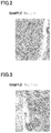
- Figs. 2 and 3 show photographs showing wetted states of the Ag paste with respect to the plating film, for the plated members of samples Nos. 1-4 and 1-11, respectively.
- a black portion represents a portion repelling the Ag paste, and a portion other than that is a portion where the Ag paste is wetted.
- Samples of plated members each including a plating film containing Au and Tl were fabricated to examine the content of Tl contained in the entire plating film and the wetted area ratio of each sample.
- Electrolytic plating was performed on surfaces of each plating target using a plating bath containing Au and Tl (samples Nos. 2-1 to 2-4).
- the plating target the same base material as that in test example 1 was used.
- a plating bath prepared by adjusting potassium gold cyanide and thallium nitrate as in test example 1 was used.
- As plating conditions Tl concentrations (in mass ratio), current densities, and temperatures shown in Fig. 2 were used. Table 2 also shows the content of Tl in each entire plating film obtained under the plating conditions. In any of the samples, the plating film had a thickness of 1 ⁇ m.
- each sample subjected to the electrolytic plating on the surfaces of the base material was subjected to heat treatment at 310° C for 1 minute in a H 2 gas atmosphere. Thereafter, each sample was left in an atmospheric air at ordinary temperature for 14 hours, and then, an Ag paste was applied thereto as in test example 1. In any of the samples, the area of applying the Ag paste was set to 3.0 mm ⁇ 2.5 mm.
- the wetted area ratio does not depend on the content of Tl contained in the entire plating film. This seems to be because, in a case where a certain amount of Tl is contained in the plating film, when the plating film is fully left after the heat treatment, Tl concentrated on the surface of the plating film by the heat treatment is fully oxidized. Since the wetted area ratio does not depend on the content of Tl contained in the entire plating film, it is expected that, by increasing the content of Tl contained in the entire plating film, the content of Au can be relatively reduced, and the cost of the plating bath can be reduced.
- 1 plated member; 2: base material: 21: first metal plate; 22: second metal plate; 23: film composed mainly of Ni; 3: plating film; 30a: crystal grain; 30b: crystal grain boundary; 31: Tl simple substance; 32: Tl oxide.
Landscapes
- Chemical & Material Sciences (AREA)
- Engineering & Computer Science (AREA)
- Materials Engineering (AREA)
- Metallurgy (AREA)
- Organic Chemistry (AREA)
- Chemical Kinetics & Catalysis (AREA)
- Mechanical Engineering (AREA)
- Electrochemistry (AREA)
- Inorganic Chemistry (AREA)
- Crystallography & Structural Chemistry (AREA)
- Electroplating Methods And Accessories (AREA)
- Electroplating And Plating Baths Therefor (AREA)
- Ceramic Engineering (AREA)
- Chemically Coating (AREA)
Abstract
Description
- The present disclosure relates to a plating film and a plated member. The present application claims priority to Japanese Patent Application No.
2018-041281 filed on March 7, 2018 -
PTL 1 discloses adding thallium as a crystal-adjusting agent into a gold plating film for coating a silver wire. - PTL 1: Japanese Patent Laying-Open No.
11-243111 - A plating film in accordance with the present disclosure is a plating film containing Au and Tl, including:
- Tl oxides including Tl2O on a surface of the plating film,
- a ratio of Tl atoms constituting Tl2O to a total of Tl atoms constituting the Tl oxides and Tl atoms constituting Tl simple substances on the surface being 40% or more.
- A plated member in accordance with the present disclosure is a plated member including a base material and a plating film coating the base material, and to be joined to a mating member via an electrically conductive joining material,
the plating film being the plating film in accordance with the present disclosure described above. -
-
Fig. 1 is a schematic configuration diagram showing a plated member in accordance with an embodiment. -
Fig. 2 is a photograph showing a wetted state between a plated member of sample No. 1-4 in test example 1 and an electrically conductive joining material. -
Fig. 3 is a photograph showing a wetted state between a plated member of sample No. 1-11 in test example 1 and the electrically conductive joining material. - A plated member including a base material coated with a plating film may be joined to a mating member via an electrically conductive joining material such as an Ag paste. On this occasion, it is desired that the plated member has an excellent wettability with the electrically conductive joining material. Specifically, it is desired that, in the plating film of the plated member, the ratio of a wetted area to the total area of a joining region with the electrically conductive joining material (wetted area ratio) is 90% or more. However, conventionally, sufficient consideration has not been given to setting the wetted area ratio to 90% or more in a gold plating film containing thallium.
- Accordingly, one object of the present disclosure is to provide a plating film excellent in wettability with an electrically conductive joining material. In addition, another object of the present disclosure is to provide a plated member excellent in wettability with an electrically conductive joining material.
- The plating film and the plated member described above are excellent in wettability with an electrically conductive joining material.
- First, the contents of an embodiment of the present disclosure will be enumerated.
- (1) A plating film in accordance with the embodiment of the present disclosure is a plating film containing Au and Tl, including Tl oxides including Tl2O on a surface of the plating film, a ratio of Tl atoms constituting Tl2O to a total of Tl atoms constituting the Tl oxides and Tl atoms constituting Tl simple substances on the surface being 40% or more.
Of the Tl oxides, Tl2O is excellent in wettability with an electrically conductive joining material. Accordingly, since the ratio of Tl atoms constituting Tl2O to the total of Tl atoms constituting the Tl oxides and Tl atoms constituting the Tl simple substances on the surface of the plating film is 40% or more, the plating film described above is excellent in wettability with the electrically conductive joining material. Specifically, the plating film described above can satisfy a ratio of a wetted area to the total area of a joining region with the electrically conductive joining material (wetted area ratio) of 90% or more. Due to excellent wettability between the plating film and the electrically conductive joining material, joining property between the plating film and a mating member via the electrically conductive joining material can be improved. - (2) As an example of the plating film described above, a content of Tl contained in the entire plating film is 10 ppm or more and 600 ppm or less in mass ratio.
Since the content of Tl contained in the entire plating film is 10 ppm or more, Tl in the plating film is easily concentrated on the surface and Tl2O is easily caused to exist on the surface of the plating film, and thus a plating film excellent in wettability with the electrically conductive joining material is easily obtained. When a large amount of Tl is contained inside the plating film, the plating film tends to be easily peeled off from a base material coated therewith. Since the content of Tl contained in the entire plating film is 600 ppm or less, it is possible to fully reduce the content of Tl inside the plating film after Tl is concentrated on the surface of the plating film, and thus peeling off of the plating film from the base material is easily suppressed. - (3) As an example of the plating film described above, the plating film has an average thickness of 0.1 µm or more.
Since the plating film has an average thickness of 0.1 µm or more, corrosion of the base material coated with the plating film due to oxidation or the like is easily suppressed. - (4) A plated member in accordance with the embodiment of the present disclosure is a plated member including a base material and a plating film coating the base material, and to be joined to a mating member via an electrically conductive joining material, the plating film being the plating film according to any of (1) to (3) described above.
Since the plated member described above includes the plating film in accordance with the embodiment of the present disclosure, it is excellent in wettability with the electrically conductive joining material, and is excellent in joining property with the mating member via the electrically conductive joining material. In addition, since the plating film is excellent in wettability with the electrically conductive joining material, a cavity is less likely to be formed between the electrically conductive joining material and the plating film, and heat resistance due to the cavity can be reduced. Since heat resistance of the electrically conductive joining material can be reduced, heat transfer between the mating member and the plated member via the electrically conductive joining material can be satisfactorily performed. For example, when the plated member is a heat dissipation member, the electrically conductive joining material is an Ag paste, and the mating member is a semiconductor chip, heat generated by the semiconductor chip can be released to the heat dissipation member via the electrically conductive joining material, and thus a failure of the semiconductor chip can be prevented. - (5) As an example of the plated member described above, the base material includes a plate material, and a film composed mainly of Ni coating the plate material, and the plate material is made of a metal including one type or more selected from Cu, Ag, Al, Mo, W, and Mg, or a composite material including one type or more selected from Cu, Ag, Al, Mo, W, and Mg and one type or more selected from diamond and silicon carbide.
- According to the configuration described above, the plated member itself is excellent in heat dissipation property. In addition, since the plate material as a main constituting member of the base material is coated with the film composed mainly of Ni, corrosion of the base material due to oxidation or the like is easily suppressed.
- Hereinafter, a plating film in accordance with the embodiment of the present disclosure, and a plated member including the plating film will be specifically described with reference to
Fig. 1 . It should be noted that the present disclosure is not limited to these examples; rather, it is defined by the scope of the claims, and is intended to include any modifications within the scope and meaning equivalent to the scope of the claims. In addition, in the present specification, an expression in the form of "A to B" means upper and lower limits of a range (that is, A or more and B or less), and when A is not accompanied by any unit and B is alone accompanied by a unit, A has the same unit as B. - A
plating film 3 in accordance with the embodiment contains Au and Tl.Plating film 3 in accordance with the embodiment has one characteristic that it includesTl oxides 32 including Tl2O on a surface of platingfilm 3, and a ratio of Tl atoms constituting Tl2O to a total of Tl atoms constituting the Tl oxides and Tl atoms constituting Tl simple substances on the surface of platingfilm 3 is 40% or more. Hereinafter, the ratio of Tl atoms constituting Tl2O to the total of Tl atoms constitutingTl oxides 32 and Tl atoms constituting Tlsimple substances 31 on the surface of platingfilm 3 is also referred to as a "ratio X". -
Plating film 3 is composed mainly of gold (Au). Being composed mainly of Au means containing 99% by mass or more of Au, and platingfilm 3 may be pure Au, or may be an Au alloy including one type or more selected from Co, Ni, Fe, Cu, Sn, Ag, and the like.Plating film 3 composed mainly of Au is excellent in electrical conductivity, joining property with a mating member via an electrically conductive joining material, corrosion resistance, and the like. -
Plating film 3 contains thallium (Tl). Tl is contained as a crystal-adjusting agent, as described in detail in a method for manufacturing the plating film described later. Tl exists within acrystal grain 30a and incrystal grain boundaries 30b of Au inside platingfilm 3, and exists on the surface of platingfilm 3. Tl existing inside platingfilm 3 typically exists as Tlsimple substances 31. Tl existing on the surface of platingfilm 3 typically exists as Tlsimple substances 31 andTl oxides 32. It should be noted that, inFig. 1 , for ease of understanding, Tlsimple substances 31 andTl oxides 32 are shown to have the same size and appropriate spacings, and are different in size and spacing from actual Tl simple substances and Tl oxides. - Tl
simple substances 31 andTl oxides 32 existing on the surface of platingfilm 3 are formed because Tlsimple substances 31 existing inside platingfilm 3 move to the surface of platingfilm 3 in the process ofmanufacturing plating film 3, as described in detail in the method for manufacturing the plating film described later. Accordingly, Tl contained in platingfilm 3 is concentrated on the surface of platingfilm 3, and mainly exists as Tlsimple substances 31 andTl oxides 32 on the surface of platingfilm 3. -
Tl oxides 32 existing on the surface of platingfilm 3 include Tl2O and Tl2O3. Tl2O contributes to improvement in the wettability between platingfilm 3 and the electrically conductive joining material. On the other hand, Tl2O3 reduces the wettability between platingfilm 3 and the electrically conductive joining material. In addition, Tlsimple substances 31 also reduce the wettability between platingfilm 3 and the electrically conductive joining material. - Tl2O existing on the surface of plating
film 3 is exposed from the surface of platingfilm 3. Tl2O existing on the surface of platingfilm 3 exists such that it adheres to the surface of platingfilm 3, or a portion thereof is embedded in platingfilm 3 and the remaining portion is exposed from platingfilm 3. Tl2O only has to be embedded in platingfilm 3 to such an extent that it can be held by platingfilm 3, and it is preferable that the portion exposed from platingfilm 3 is larger. Contact between the exposed portion of Tl2O and the electrically conductive joining material can improve the wettability. - As described above, ratio X is 40% or more in the present embodiment. Since ratio X is 40% or more, the wettability with the electrically conductive joining material can be improved, and the joining property with the mating member via the electrically conductive joining material can be improved. The more the value of ratio X is, the more the wettability with the electrically conductive joining material can be improved, and thus ratio X is 50% or more, further 60% or more, or in particular 80% or more, by way of example. It should be noted that, when ratio X exceeds a certain amount, the wettability (wetted area ratio) may be saturated.
- Ratio X can be measured by X-ray photoelectron spectroscopy (XPS). As for the Tl oxides, two types, that is, Tl2O and Tl2O3, may exist. In a narrow scan spectrum measured by XPS in the range of 110 eV to 135 eV in 0.2 eV increments, the peak of the Tl simple substances and the peak of Tl2O3 are detected at substantially the same position, and the intensity at 117.4 eV can be regarded as a height A of the intensity of the summed peak of the Tl simple substances and Tl2O3. On the other hand, the peak of Tl2O is detected to be separated from the peak of the Tl simple substances and the peak of Tl2O3, and the intensity at 118.6 eV can be regarded as a height B of the intensity of the peak of Tl2O. In the present application, ratio X is calculated as a ratio between the heights of the intensities of the peaks ({B/(A+B)} × 100).
- A content of Tl contained in
entire plating film 3 is 10 to 600 ppm in mass ratio, by way of example. Since the content of Tl contained inentire plating film 3 is 10 ppm or more, Tl in platingfilm 3 is easily concentrated on the surface of platingfilm 3, and Tl2O is easily caused to exist on the surface of platingfilm 3. On the other hand, since the content of Tl contained inentire plating film 3 is 600 ppm or less, it is possible to fully reduce the content of Tl inside platingfilm 3 after Tl is concentrated on the surface of platingfilm 3 in the process ofmanufacturing plating film 3, and thus peeling off of platingfilm 3 from the base material coated with platingfilm 3 is easily suppressed. It should be noted that ratio X has no substantial correlation with the content of Tl contained inentire plating film 3. The content of Tl contained inentire plating film 3 can be measured for example by performing inductively coupled plasma (ICP) emission spectral analysis. Specifically, platingfilm 3 is dissolved by an acid or the like, and ICP emission spectral analysis is performed using a dissolved solution as a sample. The content of Tl contained inentire plating film 3 is further 30 to 500 ppm, or in particular 60 to 400 ppm, by way of example. -
Plating film 3 has an average thickness of 0.1 µm or more, by way of example. Since platingfilm 3 has an average thickness of 0.1 µm or more, corrosion of abase material 2 coated with platingfilm 3 due to oxidation or the like is easily suppressed. On the other hand, since an increase in the average thickness of platingfilm 3 leads to an increase in cost and a decrease in industrial productivity, platingfilm 3 has an average thickness of 5.0 µm or less, by way of example. The average thickness of platingfilm 3 is obtained for example by observing cross sections in a thickness direction of platingfilm 3 at a plurality of locations (for example, five locations or more) using a scanning electron microscope (SEM) with a field of view of 3000 times, measuring thicknesses of platingfilm 3 at a plurality of uniformly spaced points (for example, ten points or more) in each microphotograph, and calculating an average in all the microphotographs. The average thickness of platingfilm 3 is further 0.3 to 3.0 µm, or in particular 0.5 to 2.0 µm, by way of example. -
Plating film 3 described abovecoats base material 2 and thereby constitutes a platedmember 1. Platedmember 1 in accordance with the embodiment is joined to the mating member via the electrically conductive joining material. Platedmember 1 is a member to be mounted on a semiconductor device, for example. Specifically, platedmember 1 is a semiconductor chip, or a heat dissipation member equipped with a semiconductor chip. The electrically conductive joining material is an Ag paste, by way of example. -
Base material 2 includes a plate material, and afilm 23 composed mainly of Ni coating the plate material. The plate material is made of a metal including one type or more selected from Cu, Ag, Al, Mo, W, and Mg, or a composite material including one type or more selected from Cu, Ag, Al, Mo, W, and Mg and one type or more selected from diamond and silicon carbide, by way of example. In the present example, the plate material has a stacked structure in which afirst metal plate 21, which is a metal plate containing Cu and is made of a Cu alloy, is sandwiched between a pair of second metal plates 22 made of Cu simple substances. As an average thickness of each offirst metal plate 21 and second metal plates 22, a desired thickness can be selected as appropriate.Film 23 composed mainly of Ni entirely coats surfaces of the plate material. Being composed mainly of Ni means containing 90% by mass or more of Ni, andfilm 23 may be pure Ni, or may be a Ni alloy including one type or more selected from Co, Pd, and the like.Film 23 composed mainly of Ni may be formed by a plating method such as Ni electroplating, Ni-P electroless plating, or Ni-B electroless plating, or may be formed by a physical vapor deposition method such as a sputtering method or a vapor deposition method.Film 23 composed mainly of Ni has an average thickness of 1.0 to 10 µm, for example. In addition, platingfilm 3 entirely coats a surface offilm 23 composed mainly of Ni. It should be noted that, inFig. 1 , for ease of understanding, each member is shown to have a thickness larger than an actual thickness. The material and the structure ofbase material 2 are not particularly limited, as long asbase material 2 is a member which can be coated with platingfilm 3 in accordance with the embodiment. - Since plated
member 1 in accordance with the embodiment includesplating film 3 in accordance with the embodiment described above on surfaces ofbase material 2, it is excellent in the wettability with the electrically conductive joining material. Specifically, in platedmember 1 in accordance with the embodiment, a wetted area ratio with respect to the electrically conductive joining material is 90% or more. The wetted area ratio is the ratio of a wetted area to the total area of a joining region between platingfilm 3 and the electrically conductive joining material. The wetted area ratio with respect to the electrically conductive joining material in platingfilm 3 can be measured for example by observing a sample which is platedmember 1 having the electrically conductive joining material adhering thereto using an optical microscope, and performing image analysis on a microphotograph thereof. Since the wetted area ratio described above is 90% or more, a cavity is less likely to be formed in a joining portion between platedmember 1 and the mating member, and platedmember 1 can be satisfactorily joined to the mating member. -
Plating film 3 and platedmember 1 described above can be manufactured by a process including a plating step, a heat treatment step, and an oxidation step. - In the plating step, plating is performed on at least a portion of surfaces of a plating target, using a plating bath containing Au and Tl, until a plating film has a desired thickness. The plating target is, for example,
base material 2 in whichfilm 23 composed mainly of Ni coats the surfaces of the plate material (seeFig. 1 ). The plating method is, for example, electrolytic plating in which the plating target (base material 2) is immersed in the plating bath for electrodeposition. When the plating is performed on only a portion of the plating target (base material 2), masking is provided to a region on which the plating is not performed. - Tl contained in the plating bath is contained as a crystal-adjusting agent. As the crystal-adjusting agent, thallium formate, thallium malonate, thallium sulfate, thallium nitrate, thallium cyanate, or the like is used, for example. The content of Tl contained in the plating bath is 0.5 to 30 ppm, by way of example. Since the content of Tl contained in the plating bath is 0.5 ppm or more, the content of Au can be relatively reduced, and the cost of the plating bath can be reduced. In addition, complexes of Au contained in the plating bath can be stabilized, and the life of the plating bath is improved and control of components constituting the plating bath can be facilitated. On the other hand, since the content of Tl contained in the plating bath is 30 ppm or less, the plating film is easily formed uniformly on the plating target (base material 2). As a composition of the plating bath, a composition of a well-known plating bath can be utilized.
- The content of Tl contained in the formed plating film, the thickness of the plating film, and the like can be adjusted by adjusting plating conditions for the plating bath, for example, by adjusting the value of a current to be applied to the plating bath, the temperature of the plating bath, and the like. Specifically, the content of Tl contained in the formed plating film can be increased by increasing the value of the current to be applied to the plating bath, and decreasing the temperature of the plating bath. The plating conditions for the plating bath are adjusted such that the content of Tl contained in the entire formed plating film is 10 to 600 ppm, by way of example.
- In the plating film formed by the plating step described above, Tl exists substantially uniformly in the thickness direction of the plating film. Specifically, Tl contained in the plating film formed by the plating step mainly exists as Tl simple substances in crystal grain boundaries of Au and may also exist within crystal grains of Au, inside the plating film. Hereinafter, the plating film formed by the plating step is referred to as a first plating film, and a plated member including the first plating film is referred to as a first plated member.
- In the heat treatment step, the first plated member described above is heat-treated in an atmosphere which does not substantially contain an oxygen element. By heat-treating the first plated member, Tl existing inside the first plating film is concentrated on a surface of the first plating film. Specifically, by heat-treating the first plated member, Au in the first plating film is recrystallized, and thereby Tl which mainly exists in the crystal grain boundaries of Au moves to the surface of the first plating film.
- The atmosphere which does not substantially contain the oxygen element means an atmosphere having an oxygen concentration of 20 ppm or less in mass ratio. The atmosphere which does not substantially contain the oxygen element is an H2 gas atmosphere, an inert gas atmosphere such as an Ar or N2 atmosphere, a mixed gas atmosphere of the H2 gas and an inert gas, or the like, by way of example.
- The heat treatment temperature is 200 to 500° C, by way of example. By setting the heat treatment temperature to 200° C or more, Au in the first plating film can be recrystallized, and at least a portion of Tl existing in the crystal grain boundaries of Au can be moved to the surface of the first plating film as Au is recrystallized. The higher the heat treatment temperature is, the more Tl existing in the crystal grain boundaries of Au can be moved to the surface of the first plating film. On the other hand, by setting the heat treatment temperature to 500° C or less, Ni in
base material 2, that is, Ni infilm 23 composed mainly of Ni can be suppressed from being diffused to the surface of the first plating film. The heat treatment temperature is further 250 to 480° C, or in particular 300 to 450° C, by way of example. - The time for maintaining heat treatment is 1 to 10 minutes, by way of example. By setting the time for maintaining the heat treatment to 1 minute or more, Au in the first plating film can be recrystallized, and at least a portion of Tl existing in the crystal grain boundaries of Au can be moved to the surface of the first plating film as Au is recrystallized. The longer the time for maintaining the heat treatment is, the more Tl existing in the crystal grain boundaries of Au can be moved to the surface of the first plating film. Au in the first plating film is fully recrystallized if the time for maintaining the heat treatment is set to 10 minutes. Accordingly, manufacturing time can be shortened by setting the time for maintaining the heat treatment to 10 minutes or less. The time for maintaining the heat treatment is further 2 to 8 minutes, or in particular 3 to 5 minutes, by way of example.
- In a plating film obtained by performing the heat treatment step on the first plating film, Tl is concentrated on a surface of the plating film. Tl existing on the surface of this plating film mainly exists as Tl simple substances immediately after the heat treatment. Hereinafter, the plating film obtained by performing the heat treatment step on the first plating film is referred to as a second plating film, and a plated member including the second plating film is referred to as a second plated member.
- In the oxidation step, the second plated member described above is left in an atmosphere containing the oxygen element. By leaving the second plated member in the atmosphere containing the oxygen element, Tl existing on a surface of the second plating film is oxidized to form Tl oxides. The Tl oxides include Tl2O and Tl2O3.
- The atmosphere containing the oxygen element means an atmosphere having an oxygen concentration of 500 ppm or more in mass ratio. The atmosphere containing the oxygen element is an atmospheric air, by way of example. Preferably, the second plated member is left in the atmosphere containing the oxygen element at ordinary temperature, because performing the oxidation step in the atmospheric air at ordinary temperature does not require special atmosphere control and temperature control. The time for leaving the second plated member in the atmosphere containing the oxygen element is 1 to 24 hours, by way of example. By setting the leaving time to 1 hour or more, of Tl existing on the surface of the second plating film, 40% or more of Tl can be oxidized to Tl2O. The remaining portion of Tl existing on the surface of the second plating film exists as Tl simple substances or is oxidized to Tl2O3. The longer the time for leaving the second plated member in the atmosphere containing the oxygen element is, the more likely Tl existing on the surface of the second plating film is oxidized to Tl2O. It should be noted that, when the leaving time exceeds a certain length, oxidation to Tl2O may be saturated. Tl in the second plating film can be fully oxidized to Tl2O if the time for leaving the second plated member in the atmosphere containing the oxygen element is set to 24 hours. Accordingly, manufacturing time can be shortened by setting the time for leaving the second plated member in the atmosphere containing the oxygen element to 24 hours or less. It should be noted that oxidation of T1 depends on external factors such as humidity. Accordingly, the time for leaving the second plated member in the atmosphere containing the oxygen element may be adjusted as appropriate according to the external factors. For example, in the case of high humidity, Tl existing on the surface of the second plating film is easily oxidized to Tl2O, and thus the leaving time can be shortened. The time for leaving the second plated member in the atmosphere containing the oxygen element is further 3 to 20 hours, or in particular 6 to 16 hours, by way of example.
-
Plating film 3 obtained by performing the oxidation step on the second plating film includesTl oxides 32 including Tl2O on the surface of platingfilm 3, as shown inFig. 1 . Ratio X in platingfilm 3 is 40% or more. It should be noted that Tl on the surface of platingfilm 3 only has to exist as Tl2O by 40% or more, and the remaining portion of Tl may take any form. - Since plating
film 3 in accordance with the embodiment includesTl oxides 32 including Tl2O on the surface thereof, and ratio X is 40% or more on the surface of platingfilm 3, the wettability with the electrically conductive joining material can be improved. Specifically, platingfilm 3 described above can satisfy a wetted area ratio with respect to the electrically conductive joining material of 90% or more. Therefore, platedmember 1 in accordance with the embodiment includingplating film 3 described above can improve the joining property with the mating member via the electrically conductive joining material. Since a wetted area ratio of 90% or more is satisfied, a cavity is less likely to be formed in the joining portion between platedmember 1 and the mating member, and heat resistance which may occur in the joining portion can be reduced. Thereby, for example when platedmember 1 is a heat dissipation member and the mating member is a semiconductor chip, heat generated by the semiconductor chip can be satisfactorily released to the heat dissipation member, and thus a failure of the semiconductor chip can be prevented. - Since the content of Tl contained in
entire plating film 3 is 10 ppm or more in platingfilm 3 in accordance with the embodiment, Tl in platingfilm 3 is easily concentrated on the surface, and Tl2O is easily caused to exist on the surface of platingfilm 3. Since Tl contained in platingfilm 3 mainly exists on the surface of platingfilm 3 and exists less inside platingfilm 3, peeling off of platingfilm 3 from the mating member coated with platingfilm 3 can be suppressed. - Samples of plated members each including a plating film containing Au and Tl were fabricated to examine the ratio of Tl2O existing on a surface of the plating film and the wetted area ratio of each sample.
- Electrolytic plating was performed on surfaces of each plating target using a plating bath containing Au and Tl (samples Nos. 1-1 to 1-4, 1-11). As the plating target, a base material formed by preparing a metal plate having a stacked structure in which a first metal plate made of a Cu-Mo based alloy was sandwiched between second metal plates made of Cu simple substances, and coating surfaces of the metal plate with a film composed mainly of Ni (Ni electroplating film) was used (see
Fig. 1 ). The base material had a size of 5.0 mm × 5.0 mm × 1.0 mm. As the plating bath, a plating bath prepared by adjusting potassium gold cyanide and thallium nitrate was used. The electrolytic plating was performed under plating conditions of a Tl concentration of 10 ppm in mass ratio, a current density of 0.5 A/dm2, and a plating bath temperature of 60° C, until a plating film had a thickness of 1.5 µm. The content of Tl in the entire plating film obtained under these plating conditions was 35 ppm in mass ratio. - Each sample subjected to the electrolytic plating on the surfaces of the base material was subjected to heat treatment at 310° C for 1 minute in a H2 gas atmosphere. Of the samples subjected to the heat treatment, samples Nos. 1-1 to 1-4 were left in an atmospheric air at ordinary temperature for leaving times shown in Table 1. Then, an Ag paste was applied to samples Nos. 1-1 to 1-4. As a method for applying the Ag paste, 50 µl of the Ag paste was dropped on each sample, and then the droplet was spread using a squeegee. The squeegeed height was 30 µm. Of the samples subjected to the heat treatment, sample No. 1-11 was not left in the atmospheric air at ordinary temperature, and the Ag paste was applied thereto immediately after the heat treatment. In any of the samples, the area of applying the Ag paste was set to 3.0 mm × 2.5 mm.
- For the plated member of each fabricated sample, the ratio of Tl atoms constituting Tl2O to the total of Tl atoms constituting Tl oxides and Tl atoms constituting Tl simple substances on a surface of the plated member was measured by XPS. Table 1 also shows the result thereof.
- For the plated member of each fabricated sample, the wetted area ratio between the plating film and the Ag paste was measured. As the wetted area ratio, the ratio of an area where the Ag paste was wetted within the area of applying the Ag paste was determined using an optical microscope. Table 1 also shows the result thereof. In addition,
Figs. 2 and 3 show photographs showing wetted states of the Ag paste with respect to the plating film, for the plated members of samples Nos. 1-4 and 1-11, respectively. InFigs. 2 and 3 , a black portion represents a portion repelling the Ag paste, and a portion other than that is a portion where the Ag paste is wetted. -
Table 1 Sample No. Leaving Time in Oxidation Step [hr] Ratio of Tl2O on Surface of Plating Film [%] Wetted Area Ratio [%] 1-1 0.5 32 85 1-2 2 53 95 1-3 8 78 98 1-4 24 99 97 1-11 0 28 80 - As shown in Table 1, in samples Nos. 1-2 to 1-4 which were left for 1 hour or more after the heat treatment and then to which the Ag paste was applied, the ratio of Tl atoms constituting Tl2O to the total of Tl atoms constituting the Tl oxides and Tl atoms constituting the Tl simple substances on the surface of the plating film was 40% or more, and the wetted area ratio was 90% or more, indicating that they are excellent in wettability. This seems to be because these samples were left for 1 hour or more after the heat treatment and thus Tl concentrated on the surface of the plating film by the heat treatment was fully oxidized. On the other hand, in sample No. 1-1 which was left for less than 1 hour after the heat treatment and then to which the Ag paste was applied, the above ratio was 32%, and the wetted area ratio was 85%, indicating that it is inferior in wettability. In addition, in sample No. 1-11 to which the Ag paste was applied immediately after the heat treatment, the above ratio was 28%, and the wetted area ratio was 80%, indicating that it is further inferior in wettability. This seems to be because these samples were left for a short period of time or were not left after the heat treatment, and thus Tl concentrated on the surface of the plating film by the heat treatment was not fully oxidized, and Tl reducing wettability, such as Tl simple substances and Tl2O3, remained on the surface of the plating film.
- Samples of plated members each including a plating film containing Au and Tl were fabricated to examine the content of Tl contained in the entire plating film and the wetted area ratio of each sample.
- Electrolytic plating was performed on surfaces of each plating target using a plating bath containing Au and Tl (samples Nos. 2-1 to 2-4). As the plating target, the same base material as that in test example 1 was used. As the plating bath, a plating bath prepared by adjusting potassium gold cyanide and thallium nitrate as in test example 1 was used. As plating conditions, Tl concentrations (in mass ratio), current densities, and temperatures shown in
Fig. 2 were used. Table 2 also shows the content of Tl in each entire plating film obtained under the plating conditions. In any of the samples, the plating film had a thickness of 1 µm. - Each sample subjected to the electrolytic plating on the surfaces of the base material was subjected to heat treatment at 310° C for 1 minute in a H2 gas atmosphere. Thereafter, each sample was left in an atmospheric air at ordinary temperature for 14 hours, and then, an Ag paste was applied thereto as in test example 1. In any of the samples, the area of applying the Ag paste was set to 3.0 mm × 2.5 mm.
- For the plated member of each fabricated sample, the content of Tl contained in the entire plating film was measured by ICP emission spectral analysis. Table 2 also shows the result thereof.
- For the plated member of each fabricated sample, the wetted area ratio between the plating film and the Ag paste was measured as in test example 1. Table 2 also shows the result thereof.
-
Table 2 Sample No. Plating Conditions Amount of Tl in Entire Plating Film [ppm] Wetted Area Ratio [%] Tl Concentration [ppm] Temperature [°C] Current Density [A/dm2] 2-1 10 60 0.5 35 99 2-2 10 60 0.8 92 95 2-3 10 40 0.5 320 96 2-4 15 40 0.5 590 97 - As shown in Table 2, it has been found that the wetted area ratio does not depend on the content of Tl contained in the entire plating film. This seems to be because, in a case where a certain amount of Tl is contained in the plating film, when the plating film is fully left after the heat treatment, Tl concentrated on the surface of the plating film by the heat treatment is fully oxidized. Since the wetted area ratio does not depend on the content of Tl contained in the entire plating film, it is expected that, by increasing the content of Tl contained in the entire plating film, the content of Au can be relatively reduced, and the cost of the plating bath can be reduced. In addition, it is also expected that, by increasing the content of Tl contained in the entire plating film, complexes of Au in the plating bath can be stabilized, and the life of the plating bath is improved and control of components constituting the plating bath can be facilitated.
- 1: plated member; 2: base material: 21: first metal plate; 22: second metal plate; 23: film composed mainly of Ni; 3: plating film; 30a: crystal grain; 30b: crystal grain boundary; 31: Tl simple substance; 32: Tl oxide.
Claims (5)
- A plating film containing Au and Tl, comprising:Tl oxides including Tl2O on a surface of the plating film,a ratio of Tl atoms constituting Tl2O to a total of Tl atoms constituting the Tl oxides and Tl atoms constituting Tl simple substances on the surface being 40% or more.
- The plating film according to claim 1, wherein a content of Tl contained in the entire plating film is 10 ppm or more and 600 ppm or less in mass ratio.
- The plating film according to claim 1 or 2, wherein the plating film has an average thickness of 0.1 µm or more.
- A plated member comprising a base material and a plating film coating the base material, and to be joined to a mating member via an electrically conductive joining material,
the plating film being the plating film according to any one of claims 1 to 3. - The plated member according to claim 4, wherein
the base material includes a plate material, and a film composed mainly of Ni coating the plate material, and
the plate material is made of a metal including one type or more selected from Cu, Ag, Al, Mo, W, and Mg, or a composite material including one type or more selected from Cu, Ag, Al, Mo, W, and Mg and one type or more selected from diamond and silicon carbide.
Applications Claiming Priority (2)
| Application Number | Priority Date | Filing Date | Title |
|---|---|---|---|
| JP2018041281 | 2018-03-07 | ||
| PCT/JP2019/007181 WO2019172010A1 (en) | 2018-03-07 | 2019-02-26 | Plating film and plated member |
Publications (2)
| Publication Number | Publication Date |
|---|---|
| EP3763851A1 true EP3763851A1 (en) | 2021-01-13 |
| EP3763851A4 EP3763851A4 (en) | 2021-12-15 |
Family
ID=67846635
Family Applications (1)
| Application Number | Title | Priority Date | Filing Date |
|---|---|---|---|
| EP19764913.0A Pending EP3763851A4 (en) | 2018-03-07 | 2019-02-26 | VENEER FILM AND VENEER ELEMENT |
Country Status (7)
| Country | Link |
|---|---|
| US (1) | US11380602B2 (en) |
| EP (1) | EP3763851A4 (en) |
| JP (1) | JP7101756B2 (en) |
| KR (1) | KR102549377B1 (en) |
| CN (1) | CN111819310B (en) |
| TW (1) | TWI813637B (en) |
| WO (1) | WO2019172010A1 (en) |
Family Cites Families (12)
| Publication number | Priority date | Publication date | Assignee | Title |
|---|---|---|---|---|
| JPS62151592A (en) * | 1985-12-25 | 1987-07-06 | Hitachi Cable Ltd | Production of gold plated lead frame |
| JPH0622252B2 (en) * | 1988-03-22 | 1994-03-23 | 山口県 | Gold plating method for electronic components for semiconductor integrated circuits |
| JPH11243111A (en) | 1998-02-25 | 1999-09-07 | Noge Denki Kogyo:Kk | Gold-plated bonding wire and method of manufacturing the same |
| JP3857928B2 (en) * | 2001-02-08 | 2006-12-13 | 京セラ株式会社 | Surface treatment method and surface-treated product of gold-plated body, method for producing gold-plated body, gold-plated body, and method for immobilizing sulfur-containing molecules |
| JP2006322037A (en) | 2005-05-18 | 2006-11-30 | Electroplating Eng Of Japan Co | Gold plating solution |
| JP5442400B2 (en) * | 2009-11-13 | 2014-03-12 | ルネサスエレクトロニクス株式会社 | Manufacturing method of semiconductor integrated circuit device |
| WO2014054429A1 (en) * | 2012-10-04 | 2014-04-10 | 日本エレクトロプレイテイング・エンジニヤース株式会社 | Non-cyanide electrolytic gold plating solution |
| JP6100203B2 (en) * | 2014-05-19 | 2017-03-22 | 日新製鋼株式会社 | Material for connecting parts |
| KR101733119B1 (en) * | 2014-08-25 | 2017-05-08 | 고지마 가가쿠 야쿠힌 가부시키가이샤 | Reduction-type electroless gold plating solution and electroless gold plating method using said plating solution |
| JP6577922B2 (en) | 2016-09-07 | 2019-09-18 | 日本電信電話株式会社 | Search apparatus, method, and program |
| WO2018117124A1 (en) * | 2016-12-19 | 2018-06-28 | 新日鐵住金株式会社 | Plated steel wire, method for producing plated steel wire, steel cord and rubber composite body |
| CN110475910A (en) * | 2017-05-22 | 2019-11-19 | 住友电气工业株式会社 | Manufacturing method of titanium-plated parts |
-
2019
- 2019-02-26 EP EP19764913.0A patent/EP3763851A4/en active Pending
- 2019-02-26 JP JP2020504936A patent/JP7101756B2/en active Active
- 2019-02-26 CN CN201980017596.7A patent/CN111819310B/en active Active
- 2019-02-26 KR KR1020207024953A patent/KR102549377B1/en active Active
- 2019-02-26 US US16/977,841 patent/US11380602B2/en active Active
- 2019-02-26 WO PCT/JP2019/007181 patent/WO2019172010A1/en not_active Ceased
- 2019-03-05 TW TW108107189A patent/TWI813637B/en active
Also Published As
| Publication number | Publication date |
|---|---|
| WO2019172010A1 (en) | 2019-09-12 |
| CN111819310A (en) | 2020-10-23 |
| JPWO2019172010A1 (en) | 2021-02-18 |
| KR20200129100A (en) | 2020-11-17 |
| TW201939630A (en) | 2019-10-01 |
| US11380602B2 (en) | 2022-07-05 |
| KR102549377B1 (en) | 2023-06-28 |
| US20210013122A1 (en) | 2021-01-14 |
| JP7101756B2 (en) | 2022-07-15 |
| EP3763851A4 (en) | 2021-12-15 |
| CN111819310B (en) | 2022-11-25 |
| TWI813637B (en) | 2023-09-01 |
Similar Documents
| Publication | Publication Date | Title |
|---|---|---|
| US7931760B2 (en) | Whiskerless plated structure and plating method | |
| KR101121117B1 (en) | Lead frame and method of producing the same | |
| EP2372800A1 (en) | Lead frame for optical semiconductor device, method for manufacturing same, and optical semiconductor device | |
| EP1932952A1 (en) | Method of surface treatment for the inhibition of wiskers | |
| EP2453491A1 (en) | Lead frame for optical semiconductor device, manufacturing method of lead frame for optical semiconductor device, and optical semiconductor device | |
| CN102575369A (en) | Electrical component and method for manufacturing electrical components | |
| CN1122300C (en) | Lead member for electronic part, and process of producing the same | |
| US11164831B2 (en) | Carrier-foil-attached ultra-thin copper foil | |
| JP2006009039A (en) | Tin-based plating film with suppressed whisker growth and method for forming the same | |
| CN101203627A (en) | Member having coating film formed thereon containing tin as main component, coating film forming method, and solder processing method | |
| TW200928006A (en) | Sn-B plating solution and plating method using it | |
| EP2433296B1 (en) | Semiconductor device contacts | |
| EP3763851A1 (en) | Plating film and plated member | |
| KR100467896B1 (en) | Cladding including copper substrate, tin cladding layer and electroplated barrier layer | |
| US11917755B2 (en) | Carrier-foil-attached ultra-thin copper foil | |
| TWI790062B (en) | Plated structure with Ni plating film and lead frame including the plated structure | |
| JP7213390B1 (en) | Silver-plated film and electrical contact provided with said silver-plated film | |
| CN105696034A (en) | Electrolyte, method of forming a copper layer and method of forming a chip | |
| JP5076088B2 (en) | Sn plated copper substrate, manufacturing method of Sn plated copper substrate, lead frame and connector terminal using the same | |
| KR830002360B1 (en) | Direct Oxide Cathode | |
| JP6438643B2 (en) | Electrode member and manufacturing method thereof | |
| JP6230732B2 (en) | Conductive strip and manufacturing method thereof |
Legal Events
| Date | Code | Title | Description |
|---|---|---|---|
| STAA | Information on the status of an ep patent application or granted ep patent |
Free format text: STATUS: THE INTERNATIONAL PUBLICATION HAS BEEN MADE |
|
| PUAI | Public reference made under article 153(3) epc to a published international application that has entered the european phase |
Free format text: ORIGINAL CODE: 0009012 |
|
| STAA | Information on the status of an ep patent application or granted ep patent |
Free format text: STATUS: REQUEST FOR EXAMINATION WAS MADE |
|
| 17P | Request for examination filed |
Effective date: 20200828 |
|
| AK | Designated contracting states |
Kind code of ref document: A1 Designated state(s): AL AT BE BG CH CY CZ DE DK EE ES FI FR GB GR HR HU IE IS IT LI LT LU LV MC MK MT NL NO PL PT RO RS SE SI SK SM TR |
|
| AX | Request for extension of the european patent |
Extension state: BA ME |
|
| DAV | Request for validation of the european patent (deleted) | ||
| DAX | Request for extension of the european patent (deleted) | ||
| RIC1 | Information provided on ipc code assigned before grant |
Ipc: H01L 21/60 20060101ALI20211027BHEP Ipc: C25D 5/00 20060101ALI20211027BHEP Ipc: C25D 5/48 20060101ALI20211027BHEP Ipc: C25D 3/48 20060101ALI20211027BHEP Ipc: C25D 5/50 20060101AFI20211027BHEP |
|
| A4 | Supplementary search report drawn up and despatched |
Effective date: 20211116 |
|
| RAP3 | Party data changed (applicant data changed or rights of an application transferred) |
Owner name: A.L.M.T. CORP. Owner name: SUMITOMO ELECTRIC INDUSTRIES, LTD. |