EP3761511A1 - Frequency multiplier, digital phase lock loop circuit and frequency multiplying method - Google Patents
Frequency multiplier, digital phase lock loop circuit and frequency multiplying method Download PDFInfo
- Publication number
- EP3761511A1 EP3761511A1 EP19775860.0A EP19775860A EP3761511A1 EP 3761511 A1 EP3761511 A1 EP 3761511A1 EP 19775860 A EP19775860 A EP 19775860A EP 3761511 A1 EP3761511 A1 EP 3761511A1
- Authority
- EP
- European Patent Office
- Prior art keywords
- signal
- duty cycle
- frequency
- cycle error
- discrete point
- Prior art date
- Legal status (The legal status is an assumption and is not a legal conclusion. Google has not performed a legal analysis and makes no representation as to the accuracy of the status listed.)
- Granted
Links
Images



Classifications
-
- H—ELECTRICITY
- H03—ELECTRONIC CIRCUITRY
- H03L—AUTOMATIC CONTROL, STARTING, SYNCHRONISATION OR STABILISATION OF GENERATORS OF ELECTRONIC OSCILLATIONS OR PULSES
- H03L7/00—Automatic control of frequency or phase; Synchronisation
- H03L7/06—Automatic control of frequency or phase; Synchronisation using a reference signal applied to a frequency- or phase-locked loop
- H03L7/08—Details of the phase-locked loop
- H03L7/099—Details of the phase-locked loop concerning mainly the controlled oscillator of the loop
- H03L7/0991—Details of the phase-locked loop concerning mainly the controlled oscillator of the loop the oscillator being a digital oscillator, e.g. composed of a fixed oscillator followed by a variable frequency divider
- H03L7/0992—Details of the phase-locked loop concerning mainly the controlled oscillator of the loop the oscillator being a digital oscillator, e.g. composed of a fixed oscillator followed by a variable frequency divider comprising a counter or a frequency divider
-
- H—ELECTRICITY
- H03—ELECTRONIC CIRCUITRY
- H03L—AUTOMATIC CONTROL, STARTING, SYNCHRONISATION OR STABILISATION OF GENERATORS OF ELECTRONIC OSCILLATIONS OR PULSES
- H03L7/00—Automatic control of frequency or phase; Synchronisation
- H03L7/06—Automatic control of frequency or phase; Synchronisation using a reference signal applied to a frequency- or phase-locked loop
- H03L7/08—Details of the phase-locked loop
- H03L7/0805—Details of the phase-locked loop the loop being adapted to provide an additional control signal for use outside the loop
-
- G—PHYSICS
- G06—COMPUTING OR CALCULATING; COUNTING
- G06F—ELECTRIC DIGITAL DATA PROCESSING
- G06F1/00—Details not covered by groups G06F3/00 - G06F13/00 and G06F21/00
- G06F1/04—Generating or distributing clock signals or signals derived directly therefrom
- G06F1/08—Clock generators with changeable or programmable clock frequency
-
- H—ELECTRICITY
- H03—ELECTRONIC CIRCUITRY
- H03B—GENERATION OF OSCILLATIONS, DIRECTLY OR BY FREQUENCY-CHANGING, BY CIRCUITS EMPLOYING ACTIVE ELEMENTS WHICH OPERATE IN A NON-SWITCHING MANNER; GENERATION OF NOISE BY SUCH CIRCUITS
- H03B19/00—Generation of oscillations by non-regenerative frequency multiplication or division of a signal from a separate source
-
- H—ELECTRICITY
- H03—ELECTRONIC CIRCUITRY
- H03K—PULSE TECHNIQUE
- H03K19/00—Logic circuits, i.e. having at least two inputs acting on one output; Inverting circuits
- H03K19/20—Logic circuits, i.e. having at least two inputs acting on one output; Inverting circuits characterised by logic function, e.g. AND, OR, NOR, NOT circuits
- H03K19/21—EXCLUSIVE-OR circuits, i.e. giving output if input signal exists at only one input; COINCIDENCE circuits, i.e. giving output only if all input signals are identical
-
- H—ELECTRICITY
- H03—ELECTRONIC CIRCUITRY
- H03K—PULSE TECHNIQUE
- H03K3/00—Circuits for generating electric pulses; Monostable, bistable or multistable circuits
- H03K3/01—Details
- H03K3/017—Adjustment of width or dutycycle of pulses
-
- H—ELECTRICITY
- H03—ELECTRONIC CIRCUITRY
- H03K—PULSE TECHNIQUE
- H03K5/00—Manipulating of pulses not covered by one of the other main groups of this subclass
- H03K5/00006—Changing the frequency
-
- H—ELECTRICITY
- H03—ELECTRONIC CIRCUITRY
- H03L—AUTOMATIC CONTROL, STARTING, SYNCHRONISATION OR STABILISATION OF GENERATORS OF ELECTRONIC OSCILLATIONS OR PULSES
- H03L7/00—Automatic control of frequency or phase; Synchronisation
- H03L7/06—Automatic control of frequency or phase; Synchronisation using a reference signal applied to a frequency- or phase-locked loop
- H03L7/08—Details of the phase-locked loop
-
- H—ELECTRICITY
- H03—ELECTRONIC CIRCUITRY
- H03L—AUTOMATIC CONTROL, STARTING, SYNCHRONISATION OR STABILISATION OF GENERATORS OF ELECTRONIC OSCILLATIONS OR PULSES
- H03L7/00—Automatic control of frequency or phase; Synchronisation
- H03L7/06—Automatic control of frequency or phase; Synchronisation using a reference signal applied to a frequency- or phase-locked loop
- H03L7/08—Details of the phase-locked loop
- H03L7/099—Details of the phase-locked loop concerning mainly the controlled oscillator of the loop
- H03L7/0991—Details of the phase-locked loop concerning mainly the controlled oscillator of the loop the oscillator being a digital oscillator, e.g. composed of a fixed oscillator followed by a variable frequency divider
-
- H—ELECTRICITY
- H03—ELECTRONIC CIRCUITRY
- H03K—PULSE TECHNIQUE
- H03K5/00—Manipulating of pulses not covered by one of the other main groups of this subclass
- H03K2005/00013—Delay, i.e. output pulse is delayed after input pulse and pulse length of output pulse is dependent on pulse length of input pulse
- H03K2005/00078—Fixed delay
-
- H—ELECTRICITY
- H03—ELECTRONIC CIRCUITRY
- H03K—PULSE TECHNIQUE
- H03K5/00—Manipulating of pulses not covered by one of the other main groups of this subclass
- H03K5/156—Arrangements in which a continuous pulse train is transformed into a train having a desired pattern
- H03K5/1565—Arrangements in which a continuous pulse train is transformed into a train having a desired pattern the output pulses having a constant duty cycle
-
- H—ELECTRICITY
- H03—ELECTRONIC CIRCUITRY
- H03L—AUTOMATIC CONTROL, STARTING, SYNCHRONISATION OR STABILISATION OF GENERATORS OF ELECTRONIC OSCILLATIONS OR PULSES
- H03L2207/00—Indexing scheme relating to automatic control of frequency or phase and to synchronisation
- H03L2207/50—All digital phase-locked loop
Definitions
- This application relates to the field of communications technologies, and in particular, to a frequency multiplier, a digital phase-locked loop circuit, and a frequency multiplication method.
- a radio frequency transceiver widely uses a frequency synthesizer of a phase-locked loop (Phase-Locked Loop, PLL) structure to generate a local oscillation signal (Local Oscillator, LO), to perform signal frequency conversion.
- Phase noises of the local oscillation signal directly affect quality of a communication signal, and affect a throughput.
- a frequency of a reference clock in a phase-locked loop is increased to improve phase noise performance of the phase-locked loop.
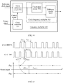
- a timing relationship between a reference clock signal and a frequency multiplied signal that is obtained after frequency multiplication may be shown in FIG. 1 .
- CLK _REF2X denotes the frequency multiplied signal that is obtained after frequency multiplication is performed on the reference clock signal CLK_REF.
- a frequency of the frequency multiplied signal is twice a frequency of the reference clock signal, but a cycle TREF2X of CLK _REF2X is only half of a cycle TREF of CLK_REF.
- Embodiments of this application provide a frequency multiplier, a digital phase-locked loop circuit, and a frequency multiplication method, to calibrate a duty cycle of a reference clock signal.
- An embodiment of this application provides a frequency multiplier, applied to a digital phase-locked loop circuit and including: a clock controller, configured to: receive an output signal of a time-to-digital converter in the digital phase-locked loop circuit, and generate a control signal based on a duty cycle error of the output signal; a clock calibration circuit, configured to: receive a reference clock signal, calibrate a duty cycle of the reference clock signal based on the control signal, and output a calibrated clock signal; and a clock frequency multiplier, configured to: receive the calibrated clock signal, multiply a frequency of the calibrated clock signal, and output a frequency multiplied signal to the time-to-digital converter.
- a clock controller configured to: receive an output signal of a time-to-digital converter in the digital phase-locked loop circuit, and generate a control signal based on a duty cycle error of the output signal
- a clock calibration circuit configured to: receive a reference clock signal, calibrate a duty cycle of the reference clock signal based on the control signal, and output
- the output signal of the time-to-digital converter may indicate a difference between the duty cycle of the reference clock signal and an ideal duty cycle
- a duty cycle error of the reference clock signal may be determined through the output signal.
- the control signal generated based on the duty cycle error can be used to accurately calibrate the duty cycle of the reference clock signal, so that a calibrated duty cycle of the reference clock signal approaches the ideal duty cycle. Therefore, the duty cycle of the reference clock signal is calibrated.
- the clock controller is specifically configured to: determine the duty cycle error based on a difference between two adjacent discrete point signals of the output signal, and perform an integral operation on the duty cycle error to obtain the control signal.
- the clock controller includes a differentiator.
- the differentiator is configured to: receive the output signal, and use a difference between a value of a k th discrete point signal of the output signal and a value of a (k-1) th discrete point signal of the output signal as a value of the k th discrete point signal in the duty cycle error, where k is a natural number greater than or equal to 1.
- the clock controller further includes a sampler and an integrator.
- the sampler is configured to sample one discrete point signal every P discrete point signals in the duty cycle error to obtain a sampled signal, where P is equal to 2n and n is an integer greater than 0.
- the integrator is configured to perform an integral operation on the sampled signal to obtain the control signal.
- the duty cycle error is sampled, which can reduce a quantity of discrete point signals used to calculate the control signal. Therefore, calculation complexity is reduced, and calculation efficiency is improved.
- the clock controller further includes an absolute value calculator and an integrator.
- the absolute value calculator is configured to: receive the duty cycle error, calculate and output an absolute value for the value of the k th discrete point signal in the duty cycle error, to obtain a duty cycle error after an absolute value operation, where k is a natural number greater than or equal to 1.
- the integrator is configured to perform an integral operation on the duty cycle error obtained after the absolute value operation, to obtain the control signal.
- the absolute value for the duty cycle error is calculated and then the integral operation is performed. Therefore, the control signal can be calculated based on a complete duty cycle error, and the obtained control signal is more accurate.
- the clock frequency multiplier includes: a clock delay circuit, configured to perform delay processing on the calibrated clock signal to obtain a delayed signal; and an XOR gate circuit, configured to: perform an XOR processing on the calibrated clock signal and the delayed signal, generate a signal obtained after the frequency of the calibrated clock signal is multiplied, and output the obtained signal to the time-to-digital converter.
- An embodiment of this application provides a digital phase-locked loop circuit, including: a time-to-digital converter, configured to generate an output signal based on a phase relationship between a frequency multiplied signal and a negative feedback clock signal, where the output signal indicates a phase difference between the frequency multiplied signal and the negative feedback clock signal; a digital loop filter, configured to perform loop filtering on the output signal to obtain an oscillator frequency control signal; a digital controlled oscillator, configured to output an oscillation signal under the control of the oscillator frequency control signal; a frequency divider, configured to perform frequency division on the oscillation signal, to obtain the negative feedback clock signal; and a frequency multiplier, configured to: receive the output signal and a reference clock signal, generate a control signal based on a duty cycle error of the output signal, calibrate a duty cycle of the reference clock signal based on the control signal to obtain a calibrated clock signal, and generate the frequency multiplied signal based on the calibrated clock signal.
- the output signal of the time-to-digital converter may indicate a difference between the duty cycle of the reference clock signal and an ideal duty cycle
- a duty cycle error of the reference clock signal may be determined through the output signal.
- the control signal generated based on the duty cycle error can be used to accurately adjust the duty cycle of the reference clock signal, so that an adjusted duty cycle of the reference clock signal approaches the ideal duty cycle. Therefore, the duty cycle of the reference clock signal is calibrated.
- the frequency multiplier is specifically configured to: determine the duty cycle error based on a difference between two adjacent discrete point signals of the output signal, and perform an integral operation on the duty cycle error to obtain the control signal.
- the frequency multiplier is specifically configured to: use a difference between a value of a k th discrete point signal of the output signal and a value of a (k-1) th discrete point signal of the output signal as a value of the k th discrete point signal in the duty cycle error, where k is a natural number greater than or equal to 1.
- the frequency multiplier is specifically configured to: sample one discrete point signal every P discrete point signals in the duty cycle error to obtain a sampled signal, where P is equal to 2n and n is an integer greater than 0; and perform an integral operation on the sampled signal to obtain the control signal.
- the frequency multiplier is specifically configured to: receive the duty cycle error, calculate and output an absolute value for a value of a k th discrete point signal in the duty cycle error, to obtain a duty cycle error after an absolute value operation, where k is a natural number greater than or equal to 1; and perform an integral operation on the duty cycle error obtained after the absolute value operation, to obtain the control signal.
- the frequency multiplier is specifically configured to: perform delay processing on the calibrated clock signal to obtain a delayed signal; and perform an XOR processing on the calibrated clock signal and the delayed signal, to generate the frequency multiplied signal.
- An embodiment of this application provides a frequency multiplication method, including: receiving an output signal of a time-to-digital converter in a digital phase-locked loop circuit, and generating a control signal based on a duty cycle error of the output signal; and calibrating a duty cycle of a received reference clock signal based on the control signal to obtain a calibrated clock signal, multiplying a frequency of the calibrated clock signal, and outputting a frequency multiplied signal.
- the output signal of the time-to-digital converter may indicate a difference between the duty cycle of the reference clock signal and an ideal duty cycle
- a duty cycle error of the reference clock signal may be determined through the output signal.
- the control signal generated based on the duty cycle error can be used to accurately adjust the duty cycle of the reference clock signal, so that an adjusted duty cycle of the reference clock signal approaches the ideal duty cycle. Therefore, the duty cycle of the reference clock signal is calibrated.
- the generating a control signal based on a duty cycle error of the output signal includes: determining the duty cycle error based on a difference between two adjacent discrete point signals of the output signal, and performing an integral operation on the duty cycle error to obtain the control signal.
- the determining the duty cycle error based on a difference between two adjacent discrete point signals of the output signal includes: using a difference between a value of a k th discrete point signal of the output signal and a value of a (k-1) th discrete point signal of the output signal as a value of the k th discrete point signal in the duty cycle error, to obtain the duty cycle error, where k is a natural number greater than or equal to 1.
- the performing an integral operation on the duty cycle error to obtain the control signal includes: sampling one discrete point signal every P discrete point signals in the duty cycle error to obtain a sampled signal, where P is equal to 2n and n is an integer greater than 0; and performing an integral operation on the sampled signal to obtain the control signal.
- the performing an integral operation on the duty cycle error to obtain the control signal includes: calculating and outputting an absolute value for a value of a k th discrete point signal in the duty cycle error, to obtain a duty cycle error after an absolute value operation, where k is a natural number greater than or equal to 1; and performing an integral operation on the duty cycle error obtained after the absolute value operation, to obtain the control signal.
- the multiplying a frequency of the calibrated clock signal includes: performing delay processing on the calibrated clock signal to obtain a delayed signal; and performing an XOR processing on the calibrated clock signal and the delayed signal, to obtain a signal that is obtained after the frequency of the calibrated clock signal is multiplied.
- FIG. 3 is a schematic structural diagram of a digital phase-locked loop circuit according to an embodiment of this application.
- the digital phase-locked loop circuit shown in FIG. 3 includes a frequency multiplier 401, a time-to-digital converter (Time to Digital Convert, TDC) 402, a digital loop filter (Digital Loop Filter, DLF) 403, a digital controlled oscillator (Digital Controlled Oscillator, DCO) 404, and a frequency divider (divider, DIV) 405.
- TDC Time to Digital Convert
- DLF Digital Loop Filter
- DCO Digital Controlled Oscillator
- DIV frequency divider
- An output signal of the time-to-digital converter 402 is a discrete signal.
- the time-to-digital converter 402 is configured to generate the output signal based on a phase relationship between a frequency multiplied signal and a negative feedback clock signal.
- the output signal indicates a phase difference between the frequency multiplied signal and the negative feedback clock signal.
- the digital loop filter 403 is configured to perform loop filtering on the output signal to obtain an oscillator frequency control signal.
- the digital controlled oscillator 404 is configured to output an oscillation signal under the control of the oscillator frequency control signal.
- the frequency divider 405 is configured to perform frequency division on the oscillation signal, to obtain the negative feedback clock signal.
- the frequency multiplier 401 is configured to: receive the output signal and a reference clock signal, generate a control signal based on a duty cycle error of the output signal, calibrate a duty cycle of the reference clock signal based on the control signal to obtain a calibrated clock signal, and generate the frequency multiplied signal based on the calibrated clock signal.
- the frequency multiplied signal is a signal obtained after a frequency of the calibrated clock signal is multiplied.
- the frequency multiplier 401 outputs the frequency multiplied signal to the time-to-digital converter 402.
- the frequency multiplier 401 further receives the output signal of the time-to-digital converter 402, and adjusts the duty cycle of the reference clock signal based on the output signal of the time-to-digital converter 402. In this way, the duty cycle of the reference clock signal is adjusted to 50%. Therefore, a problem that a spurious signal occurs in output signals of the digital phase-locked loop circuit when the duty cycle of the reference clock signal is not 50% is resolved. Details are described below.
- the frequency multiplier 401 shown in FIG. 4 includes a clock controller 501, a clock calibration circuit 502, and a clock frequency multiplier 503.
- the clock controller 501 is configured to: receive an output signal of a time-to-digital converter in a digital phase-locked loop circuit, and generate a control signal based on a duty cycle error of the output signal.
- the clock calibration circuit 502 is configured to: receive a reference clock signal, calibrate a duty cycle of the reference clock signal based on the control signal, and output a calibrated clock signal.
- the clock frequency multiplier 503 is configured to: receive the calibrated clock signal, multiply a frequency of the calibrated clock signal, and output a frequency multiplied signal to the time-to-digital converter.
- the clock frequency multiplier 503 may include a clock delay circuit 5031 and an XOR gate circuit 5032.
- the clock delay circuit 5031 is connected to an output end of the clock calibration circuit 502, and performs delay processing on a received clock signal that is calibrated by the clock calibration circuit 502, and then outputs a signal obtained after delay processing to the XOR gate circuit 5032.
- An input end of the XOR gate circuit 5032 is connected to an output end of the clock delay circuit 5031, and another output end of the XOR gate circuit 5032 is connected to the output end of the clock calibration circuit 502. After performing XOR processing on signals received through the two input ends, the XOR gate circuit 5032 obtains a frequency multiplied signal and outputs the frequency multiplied signal to the time-to-digital converter.
- an output signal of the time-to-digital converter 402 in the digital phase-locked loop circuit is a discrete signal, and an absolute value for a value of each discrete point signal of the output signal of the time-to-digital converter 402 is proportional to a duty cycle error of a reference clock signal.
- the duty cycle error of the reference clock signal CLK _REF is equal to a difference between the duty cycle of the reference clock signal CLK_REF and an ideal duty cycle (that is, 50%).
- input signals of the time-to-digital converter 402 are a frequency multiplied signal CLK_REF2X and a negative feedback clock signal CLK_DIV
- the frequency multiplied signal CLK_REF2X is a signal output after the frequency multiplier 401 multiplies a frequency of the reference clock signal.
- the negative feedback clock signal CLK_DIV is a signal that is output after the frequency divider 405 performs frequency division processing on an output signal of the digital phase-locked loop circuit 402.
- K TDC denotes a conversion gain of the time-to-digital converter 402, and K TDC is a preset value.
- ⁇ k denotes the phase difference between the frequency multiplied signal CLK_REF2X and the negative feedback clock signal CLK_DIV.
- T REF 2 X denotes a clock cycle of the negative feedback clock signal CLK_DIV and is half of a clock cycle of the reference clock signal.
- FIG. 5 is a schematic diagram of a signal according to an embodiment of this application.
- Two adjacent clock cycles, namely, T R2A and T R2B , of the frequency multiplied signal CLK _REF2X alternate when the duty cycle of the reference clock signal is not 50%.
- the phase difference between the frequency multiplied signal CLK _REF2X and the negative feedback clock signal CLK_DIV that are received by the time-to-digital converter in the digital phase-locked loop circuit is not 0 in each clock cycle, but alternates between ⁇ ERR and - ⁇ ERR ⁇
- the time-to-digital converter 402 outputs R TDC when the phase difference between the frequency multiplied signal CLK _REF2X and the negative feedback clock signal CLK_DIV is ⁇ ERR ⁇
- the time-to-digital converter 402 outputs -R TDC when the phase difference between the frequency multiplied signal CLK _REF2X and the negative feedback clock signal CLK_DIV is - ⁇ ERR ⁇
- An absolute value for a difference between values of two adjacent discrete point signals of the output signal of the time-to-digital converter 402 is ⁇ R TDC .
- a value of ⁇ R TDC is proportional to the duty cycle error of the reference clock signal CLK_REF.
- a larger duty cycle error of the reference clock signal CLK _REF indicates a larger ⁇ R TDC
- a smaller duty cycle error of the reference clock signal CLK_REF indicates a smaller ⁇ R TDC ⁇
- the clock controller 501 may determine the duty cycle error based on the output signal of the time-to-digital converter 402, and then determine a control signal based on the duty cycle error.
- the duty cycle error indicates a value of the duty cycle error of the reference clock signal CLK REF received by the digital phase-locked loop circuit.
- the clock controller 501 may determine the duty cycle error based on the difference between two adjacent discrete point signals of the output signal, and perform an integral operation on the duty cycle error to obtain the control signal. Details are described below based on different scenarios.
- the clock controller 501 includes a differentiator 701, a sampler 702, and an integrator 703.
- the differentiator 701 is configured to: receive an output signals of a time-to-digital converter, and use a difference between a value of a k th discrete point signal of the output signal and a value of a (k-1) th discrete point signal of the output signal as a value of the k th discrete point signal in the duty cycle error.
- R TDC [ k ] is the value of the k th discrete point signal of the output signal of the time-to-digital converter.
- R TDC [ k -1] is the value of the (k-1) th discrete point signal of the output signal of the time-to-digital converter.
- the duty cycle error output by the differentiator 701 actually consists of ⁇ R TDC and - ⁇ R TDC that alternate.
- ⁇ R TDC is an absolute value for a difference between -R TDC and R TDC .
- the sampler 702 is configured to: receive the duty cycle error and sample one discrete point signal every P discrete point signals in the duty cycle error to obtain a sampled signal.
- P is equal to 2n and n is an integer greater than 0.
- the integrator 703 is configured to: receive the sampled signal and perform an integral operation on the sampled signal to obtain the control signal.
- K DCC is a duty cycle control coefficient, and a specific value of the duty cycle control coefficient depends on an actual situation.
- the clock controller 501 includes a differentiator 801, an absolute value calculator 802, and an integrator 803.
- the integrator 803 is configured to perform an integral operation on the duty cycle error obtained after the absolute value operation, to obtain the control signal.
- K DCC is a duty cycle control coefficient
- the clock controller 501 may further determine the duty cycle error based on a difference between values of two discrete point signals that are of the output signal and m discrete points apart, and perform an integral operation on the duty cycle error to obtain the control signal, where m is an odd number.
- the differentiator 701 is configured to: receive the output signal of the time-to-digital converter, and use a difference between the value of the k th discrete point signal of the output signal and a value of a (k-m) th discrete point signal of the output signal as the value of the k th discrete point signal in the duty cycle error.
- the clock calibration circuit 502 After the clock controller 501 outputs the generated control signal DCC CTRL to the clock calibration circuit 502, the clock calibration circuit 502 adjusts the duty cycle of the reference clock signal based on the control signal, and outputs the calibrated clock signal.
- a duty cycle of the calibrated clock signal output by the clock calibration circuit 502 is in a negative feedback relationship with the input control signal.
- a manner used by the clock calibration circuit 502 to adjust the duty cycle of the reference clock signal based on the control signal output by the clock controller 501 is not limited in this embodiment of this application.
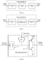
- the clock calibration circuit 502 may be shown in FIG. 8 .
- the clock calibration circuit shown in FIG. 8 includes a capacitor 901, a digital analog converter (digital to analog converter, DAC) 902, an output buffer 903, and the like.
- a control signal DCC CTRL is equivalent to a bias voltage for the output buffer 903.
- the output buffer 903 outputs control signals with different duty cycles, and a duty cycle of a calibrated clock signal CLK_REF_DCC output by the clock calibration circuit 502 is in a negative feedback relationship with an input control signal.
- a relatively large duty cycle of a reference clock signal CLK_REF_DCC input by the clock calibration circuit 502 indicates a relatively large duty cycle error of the reference clock signal CLK_REF_DCC.
- the duty cycle error of the reference clock signal CLK_REF_DCC is equal to a difference between the duty cycle of the reference clock signal CLK_REF_DCC and 50%. Then, it can be learned from the circuit shown in FIG. 3 or FIG. 4 that an absolute value ⁇ R TDC for a difference between values of two adjacent discrete point signals of an output signal of a time-to-digital converter is larger. Further, a value of the control signal DCC_CTRL output by the clock controller is larger according to formula (4).
- a duty cycle of a signal output by the output buffer 903 is smaller. Because of the negative feedback relationship, a duty cycle of the calibrated clock signal generated after the clock calibration circuit adjusts the reference clock signal CLK_REF_DCC based on the control signal approaches 50%. In this way, the duty cycle of the reference clock signal is calibrated.
- FIG. 8 is merely an example and the clock calibration circuit 502 may alternatively be implemented in another manner.
- the clock calibration circuit 502 may be a delay chain circuit. Details are not described herein.
- An embodiment of this application further provides a frequency multiplication method, which may be applied to a digital phase-locked loop circuit.
- the method is used to adjust a duty cycle of a received reference clock signal in the digital phase-locked loop circuit, to obtain a reference clock signal with a duty cycle of 50%. Therefore, a problem that a spurious signal occurs in output signals of the digital phase-locked loop circuit when the duty cycle of the reference clock signal is not 50% is resolved.
- the method includes the following steps.
- Step 1001 Receive an output signal of a time-to-digital converter in the digital phase-locked loop circuit, and generate a control signal based on a duty cycle error of the output signal.
- the duty cycle error may be determined based on a difference between two adjacent discrete point signals of the output signal. Details are as follows:
- a difference between a value of a k th discrete point signal of the output signal and a value of a (k-m) th discrete point signal of the output signal as a value of the k th discrete point signal in the duty cycle error to obtain the duty cycle error, where k is a natural number greater than or equal to 1. m is an odd number.
- control signal may be obtained in any one of the following manners:
- one discrete point signal may be sampled every P discrete point signals in the duty cycle error to obtain a sampled signal, where P is equal to 2n and n is an integer greater than 0.
- control signal is determined based on a result of an integral operation performed on the duty cycle error includes:
- An absolute value for the value of the k th discrete point signal in the duty cycle error is calculated and output, to obtain a duty cycle error after an absolute value operation, where k is a natural number greater than or equal to 1.
- Step 1002 Calibrate the duty cycle of the received reference clock signal based on the control signal to obtain a calibrated clock signal, multiply a frequency of the calibrated clock signal, and output a frequency multiplied signal.
- Step 1001 and step 1002 may be performed by a frequency multiplier in the digital phase-locked loop circuit.
- a frequency multiplier in the digital phase-locked loop circuit.
- FIG. 4 For details, refer to the frequency multiplier shown in FIG. 4 . Details are not described herein.
- the time-to-digital converter in the digital phase-locked loop circuit may output an output signal based on a phase relationship between a calibrated clock signal obtained after frequency multiplication and a negative feedback clock signal.
- the output signal indicates a phase difference between the frequency multiplied signal and the negative feedback clock signal.
- a digital loop filter in the digital phase-locked loop circuit is configured to perform loop filtering on the output signal to obtain an oscillator frequency control signal.
- a digital controlled oscillator in the digital phase-locked loop circuit is configured to output an oscillation signal under the control of the oscillator frequency control signal.
- a frequency divider in the digital phase-locked loop circuit is configured to perform frequency division on the oscillation signal, to obtain the negative feedback clock signal.
Landscapes
- Physics & Mathematics (AREA)
- Engineering & Computer Science (AREA)
- General Engineering & Computer Science (AREA)
- Theoretical Computer Science (AREA)
- Nonlinear Science (AREA)
- Computer Hardware Design (AREA)
- Computing Systems (AREA)
- Mathematical Physics (AREA)
- General Physics & Mathematics (AREA)
- Stabilization Of Oscillater, Synchronisation, Frequency Synthesizers (AREA)
- Manipulation Of Pulses (AREA)
Abstract
Description
- This application claims priority to Chinese Patent Application No.
201810278768.3 - This application relates to the field of communications technologies, and in particular, to a frequency multiplier, a digital phase-locked loop circuit, and a frequency multiplication method.
- A radio frequency transceiver widely uses a frequency synthesizer of a phase-locked loop (Phase-Locked Loop, PLL) structure to generate a local oscillation signal (Local Oscillator, LO), to perform signal frequency conversion. Phase noises of the local oscillation signal directly affect quality of a communication signal, and affect a throughput. In the prior art, a frequency of a reference clock in a phase-locked loop is increased to improve phase noise performance of the phase-locked loop. Ideally, a timing relationship between a reference clock signal and a frequency multiplied signal that is obtained after frequency multiplication may be shown in
FIG. 1 . CLK _REF2X denotes the frequency multiplied signal that is obtained after frequency multiplication is performed on the reference clock signal CLK_REF. A frequency of the frequency multiplied signal is twice a frequency of the reference clock signal, but a cycle TREF2X of CLK _REF2X is only half of a cycle TREF of CLK_REF. - However, quality of an output signal in a clock frequency multiplier circuit in the prior art heavily relies on a duty cycle of an input reference clock signal. Two adjacent clock cycles of the output signal CLK_REF2X in the clock frequency multiplier circuit alternate when the duty cycle of the input reference clock signal is not 50%. For details, refer to
FIG. 2 . InFIG. 2 , the two adjacent clock cycles of CLK _REF2X are TR2A and TR2B respectively, and TR2A is less than TR2B. Such an alternating clock cycle is equivalent to a result of introducing a high-frequency frequency modulation signal to the reference clock signal. Consequently, a spurious signal may occur in output signals in the phase-locked loop circuit. This compromises performance of a radio frequency communications system. - Therefore, how to calibrate the duty cycle of the reference clock signal is an urgent problem to be resolved.
- Embodiments of this application provide a frequency multiplier, a digital phase-locked loop circuit, and a frequency multiplication method, to calibrate a duty cycle of a reference clock signal.
- An embodiment of this application provides a frequency multiplier, applied to a digital phase-locked loop circuit and including: a clock controller, configured to: receive an output signal of a time-to-digital converter in the digital phase-locked loop circuit, and generate a control signal based on a duty cycle error of the output signal; a clock calibration circuit, configured to: receive a reference clock signal, calibrate a duty cycle of the reference clock signal based on the control signal, and output a calibrated clock signal; and a clock frequency multiplier, configured to: receive the calibrated clock signal, multiply a frequency of the calibrated clock signal, and output a frequency multiplied signal to the time-to-digital converter.
- In the foregoing solution, because the output signal of the time-to-digital converter may indicate a difference between the duty cycle of the reference clock signal and an ideal duty cycle, a duty cycle error of the reference clock signal may be determined through the output signal. In this way, the control signal generated based on the duty cycle error can be used to accurately calibrate the duty cycle of the reference clock signal, so that a calibrated duty cycle of the reference clock signal approaches the ideal duty cycle. Therefore, the duty cycle of the reference clock signal is calibrated.
- In an optional implementation, the clock controller is specifically configured to: determine the duty cycle error based on a difference between two adjacent discrete point signals of the output signal, and perform an integral operation on the duty cycle error to obtain the control signal.
- In an optional implementation, the clock controller includes a differentiator. The differentiator is configured to: receive the output signal, and use a difference between a value of a kth discrete point signal of the output signal and a value of a (k-1)th discrete point signal of the output signal as a value of the kth discrete point signal in the duty cycle error, where k is a natural number greater than or equal to 1.
- In an optional implementation, the clock controller further includes a sampler and an integrator. The sampler is configured to sample one discrete point signal every P discrete point signals in the duty cycle error to obtain a sampled signal, where P is equal to 2n and n is an integer greater than 0. The integrator is configured to perform an integral operation on the sampled signal to obtain the control signal.
- In the foregoing solution, the duty cycle error is sampled, which can reduce a quantity of discrete point signals used to calculate the control signal. Therefore, calculation complexity is reduced, and calculation efficiency is improved.
- In an optional implementation, the clock controller further includes an absolute value calculator and an integrator. The absolute value calculator is configured to: receive the duty cycle error, calculate and output an absolute value for the value of the kth discrete point signal in the duty cycle error, to obtain a duty cycle error after an absolute value operation, where k is a natural number greater than or equal to 1. The integrator is configured to perform an integral operation on the duty cycle error obtained after the absolute value operation, to obtain the control signal.
- In the foregoing solution, the absolute value for the duty cycle error is calculated and then the integral operation is performed. Therefore, the control signal can be calculated based on a complete duty cycle error, and the obtained control signal is more accurate.
- In an optional implementation, the clock frequency multiplier includes: a clock delay circuit, configured to perform delay processing on the calibrated clock signal to obtain a delayed signal; and an XOR gate circuit, configured to: perform an XOR processing on the calibrated clock signal and the delayed signal, generate a signal obtained after the frequency of the calibrated clock signal is multiplied, and output the obtained signal to the time-to-digital converter.
- An embodiment of this application provides a digital phase-locked loop circuit, including: a time-to-digital converter, configured to generate an output signal based on a phase relationship between a frequency multiplied signal and a negative feedback clock signal, where the output signal indicates a phase difference between the frequency multiplied signal and the negative feedback clock signal; a digital loop filter, configured to perform loop filtering on the output signal to obtain an oscillator frequency control signal; a digital controlled oscillator, configured to output an oscillation signal under the control of the oscillator frequency control signal; a frequency divider, configured to perform frequency division on the oscillation signal, to obtain the negative feedback clock signal; and a frequency multiplier, configured to: receive the output signal and a reference clock signal, generate a control signal based on a duty cycle error of the output signal, calibrate a duty cycle of the reference clock signal based on the control signal to obtain a calibrated clock signal, and generate the frequency multiplied signal based on the calibrated clock signal.
- In the foregoing solution, because the output signal of the time-to-digital converter may indicate a difference between the duty cycle of the reference clock signal and an ideal duty cycle, a duty cycle error of the reference clock signal may be determined through the output signal. In this way, the control signal generated based on the duty cycle error can be used to accurately adjust the duty cycle of the reference clock signal, so that an adjusted duty cycle of the reference clock signal approaches the ideal duty cycle. Therefore, the duty cycle of the reference clock signal is calibrated.
- In an optional implementation, the frequency multiplier is specifically configured to: determine the duty cycle error based on a difference between two adjacent discrete point signals of the output signal, and perform an integral operation on the duty cycle error to obtain the control signal.
- In an optional implementation, the frequency multiplier is specifically configured to: use a difference between a value of a kth discrete point signal of the output signal and a value of a (k-1)th discrete point signal of the output signal as a value of the kth discrete point signal in the duty cycle error, where k is a natural number greater than or equal to 1.
- In an optional implementation, the frequency multiplier is specifically configured to: sample one discrete point signal every P discrete point signals in the duty cycle error to obtain a sampled signal, where P is equal to 2n and n is an integer greater than 0; and perform an integral operation on the sampled signal to obtain the control signal.
- In an optional implementation, the frequency multiplier is specifically configured to: receive the duty cycle error, calculate and output an absolute value for a value of a kth discrete point signal in the duty cycle error, to obtain a duty cycle error after an absolute value operation, where k is a natural number greater than or equal to 1; and perform an integral operation on the duty cycle error obtained after the absolute value operation, to obtain the control signal.
- In an optional implementation, the frequency multiplier is specifically configured to: perform delay processing on the calibrated clock signal to obtain a delayed signal; and perform an XOR processing on the calibrated clock signal and the delayed signal, to generate the frequency multiplied signal.
- An embodiment of this application provides a frequency multiplication method, including: receiving an output signal of a time-to-digital converter in a digital phase-locked loop circuit, and generating a control signal based on a duty cycle error of the output signal; and calibrating a duty cycle of a received reference clock signal based on the control signal to obtain a calibrated clock signal, multiplying a frequency of the calibrated clock signal, and outputting a frequency multiplied signal.
- In the foregoing solution, because the output signal of the time-to-digital converter may indicate a difference between the duty cycle of the reference clock signal and an ideal duty cycle, a duty cycle error of the reference clock signal may be determined through the output signal. In this way, the control signal generated based on the duty cycle error can be used to accurately adjust the duty cycle of the reference clock signal, so that an adjusted duty cycle of the reference clock signal approaches the ideal duty cycle. Therefore, the duty cycle of the reference clock signal is calibrated.
- In an optional implementation, the generating a control signal based on a duty cycle error of the output signal includes: determining the duty cycle error based on a difference between two adjacent discrete point signals of the output signal, and performing an integral operation on the duty cycle error to obtain the control signal.
- In an optional implementation, the determining the duty cycle error based on a difference between two adjacent discrete point signals of the output signal includes: using a difference between a value of a kth discrete point signal of the output signal and a value of a (k-1)th discrete point signal of the output signal as a value of the kth discrete point signal in the duty cycle error, to obtain the duty cycle error, where k is a natural number greater than or equal to 1.
- In an optional implementation, the performing an integral operation on the duty cycle error to obtain the control signal includes: sampling one discrete point signal every P discrete point signals in the duty cycle error to obtain a sampled signal, where P is equal to 2n and n is an integer greater than 0; and performing an integral operation on the sampled signal to obtain the control signal.
- In an optional implementation, the performing an integral operation on the duty cycle error to obtain the control signal includes: calculating and outputting an absolute value for a value of a kth discrete point signal in the duty cycle error, to obtain a duty cycle error after an absolute value operation, where k is a natural number greater than or equal to 1; and performing an integral operation on the duty cycle error obtained after the absolute value operation, to obtain the control signal.
- In an optional implementation manner, the multiplying a frequency of the calibrated clock signal includes: performing delay processing on the calibrated clock signal to obtain a delayed signal; and performing an XOR processing on the calibrated clock signal and the delayed signal, to obtain a signal that is obtained after the frequency of the calibrated clock signal is multiplied.
-
-
FIG. 1 is a schematic diagram of a reference clock signal according to an embodiment of this application; -
FIG. 2 is a schematic diagram of an output signal of a clock frequency multiplier circuit according to an embodiment of this application; -
FIG. 3 is a schematic structural diagram of a digital phase-locked loop circuit according to an embodiment of this application; -
FIG. 4 is a schematic structural diagram of a frequency multiplier according to an embodiment of this application; -
FIG. 5 is a schematic diagram of a signal according to an embodiment of this application; -
FIG. 6 is a schematic structural diagram of a clock controller according to an embodiment of this application; -
FIG. 7 is a schematic structural diagram of a clock controller according to an embodiment of this application; -
FIG. 8 is a schematic structural diagram of a clock calibration circuit according to an embodiment of this application; and -
FIG. 9 is a schematic flowchart of a frequency multiplication method according to an embodiment of this application. - The following describes the embodiments of this application in detail with reference to the accompanying drawings in this specification.
- A frequency multiplier provided in the embodiments of this application may be applied to a digital phase-locked loop circuit.
FIG. 3 is a schematic structural diagram of a digital phase-locked loop circuit according to an embodiment of this application. The digital phase-locked loop circuit shown inFIG. 3 includes afrequency multiplier 401, a time-to-digital converter (Time to Digital Convert, TDC) 402, a digital loop filter (Digital Loop Filter, DLF) 403, a digital controlled oscillator (Digital Controlled Oscillator, DCO) 404, and a frequency divider (divider, DIV) 405. - An output signal of the time-to-
digital converter 402 is a discrete signal. - The time-to-
digital converter 402 is configured to generate the output signal based on a phase relationship between a frequency multiplied signal and a negative feedback clock signal. The output signal indicates a phase difference between the frequency multiplied signal and the negative feedback clock signal. - The
digital loop filter 403 is configured to perform loop filtering on the output signal to obtain an oscillator frequency control signal. - The digital controlled
oscillator 404 is configured to output an oscillation signal under the control of the oscillator frequency control signal. - The
frequency divider 405 is configured to perform frequency division on the oscillation signal, to obtain the negative feedback clock signal. - The
frequency multiplier 401 is configured to: receive the output signal and a reference clock signal, generate a control signal based on a duty cycle error of the output signal, calibrate a duty cycle of the reference clock signal based on the control signal to obtain a calibrated clock signal, and generate the frequency multiplied signal based on the calibrated clock signal. The frequency multiplied signal is a signal obtained after a frequency of the calibrated clock signal is multiplied. - As described above, after doubling the frequency of the received reference clock signal, the
frequency multiplier 401 outputs the frequency multiplied signal to the time-to-digital converter 402. In this embodiment of this application, thefrequency multiplier 401 further receives the output signal of the time-to-digital converter 402, and adjusts the duty cycle of the reference clock signal based on the output signal of the time-to-digital converter 402. In this way, the duty cycle of the reference clock signal is adjusted to 50%. Therefore, a problem that a spurious signal occurs in output signals of the digital phase-locked loop circuit when the duty cycle of the reference clock signal is not 50% is resolved. Details are described below. - It should be noted that, for functions and specific implementations of other modules in the digital phase-locked loop circuit shown in
FIG. 3 , refer to descriptions in the prior art. Details are not described in this embodiment of this application. - With reference to
FIG. 3 , a structure of thefrequency multiplier 401 inFIG. 3 may be shown inFIG. 4 . Thefrequency multiplier 401 shown inFIG. 4 includes aclock controller 501, aclock calibration circuit 502, and aclock frequency multiplier 503. - The
clock controller 501 is configured to: receive an output signal of a time-to-digital converter in a digital phase-locked loop circuit, and generate a control signal based on a duty cycle error of the output signal. - The
clock calibration circuit 502 is configured to: receive a reference clock signal, calibrate a duty cycle of the reference clock signal based on the control signal, and output a calibrated clock signal. - The
clock frequency multiplier 503 is configured to: receive the calibrated clock signal, multiply a frequency of the calibrated clock signal, and output a frequency multiplied signal to the time-to-digital converter. - In this embodiment of this application, the
clock frequency multiplier 503 may include aclock delay circuit 5031 and anXOR gate circuit 5032. - The
clock delay circuit 5031 is connected to an output end of theclock calibration circuit 502, and performs delay processing on a received clock signal that is calibrated by theclock calibration circuit 502, and then outputs a signal obtained after delay processing to theXOR gate circuit 5032. An input end of theXOR gate circuit 5032 is connected to an output end of theclock delay circuit 5031, and another output end of theXOR gate circuit 5032 is connected to the output end of theclock calibration circuit 502. After performing XOR processing on signals received through the two input ends, theXOR gate circuit 5032 obtains a frequency multiplied signal and outputs the frequency multiplied signal to the time-to-digital converter. - It should be noted that specific implementations of the
clock delay circuit 5031 and theXOR gate circuit 5032 are not limited in this embodiment of this application, and details are not described herein. - In an embodiment of this application, an output signal of the time-to-
digital converter 402 in the digital phase-locked loop circuit is a discrete signal, and an absolute value for a value of each discrete point signal of the output signal of the time-to-digital converter 402 is proportional to a duty cycle error of a reference clock signal. The duty cycle error of the reference clock signal CLK _REF is equal to a difference between the duty cycle of the reference clock signal CLK_REF and an ideal duty cycle (that is, 50%). - With reference to
FIG. 3 , input signals of the time-to-digital converter 402 are a frequency multiplied signal CLK_REF2X and a negative feedback clock signal CLK_DIV The frequency multiplied signal CLK_REF2X is a signal output after thefrequency multiplier 401 multiplies a frequency of the reference clock signal. The negative feedback clock signal CLK_DIV is a signal that is output after thefrequency divider 405 performs frequency division processing on an output signal of the digital phase-lockedloop circuit 402. - The time-to-
digital converter 402 determines a phase difference between the frequency multiplied signal CLK_REF2X and the negative feedback clock signal CLK_DIV in each clock cycle, and determines the output signal based on the phase difference. Specifically, a value RTDC[k] of a kth discrete point signal of the output signal of the time-to-digital converter 402 satisfies the following formula:
- KTDC denotes a conversion gain of the time-to-
digital converter 402, and KTDC is a preset value. ϕk denotes the phase difference between the frequency multiplied signal CLK_REF2X and the negative feedback clock signal CLK_DIV. T REF2X denotes a clock cycle of the negative feedback clock signal CLK_DIV and is half of a clock cycle of the reference clock signal. - Specifically,
FIG. 5 is a schematic diagram of a signal according to an embodiment of this application. Two adjacent clock cycles, namely, TR2A and TR2B, of the frequency multiplied signal CLK _REF2X alternate when the duty cycle of the reference clock signal is not 50%. When the digital phase-locked loop circuit is in a locked state, the phase difference between the frequency multiplied signal CLK _REF2X and the negative feedback clock signal CLK_DIV that are received by the time-to-digital converter in the digital phase-locked loop circuit is not 0 in each clock cycle, but alternates between ϕERR and -ϕERR· The time-to-digital converter 402 outputs RTDC when the phase difference between the frequency multiplied signal CLK _REF2X and the negative feedback clock signal CLK_DIV is ϕERR· The time-to-digital converter 402 outputs -RTDC when the phase difference between the frequency multiplied signal CLK _REF2X and the negative feedback clock signal CLK_DIV is -ϕERR· An absolute value for a difference between values of two adjacent discrete point signals of the output signal of the time-to-digital converter 402 is ΔRTDC. A value of ΔRTDC is proportional to the duty cycle error of the reference clock signal CLK_REF. A larger duty cycle error of the reference clock signal CLK _REF indicates a larger ΔRTDC, and a smaller duty cycle error of the reference clock signal CLK_REF indicates a smaller ΔRTDC· - In this embodiment of this application, the
clock controller 501 may determine the duty cycle error based on the output signal of the time-to-digital converter 402, and then determine a control signal based on the duty cycle error. The duty cycle error indicates a value of the duty cycle error of the reference clock signal CLK REF received by the digital phase-locked loop circuit. - In this embodiment of this application, the
clock controller 501 may determine the duty cycle error based on the difference between two adjacent discrete point signals of the output signal, and perform an integral operation on the duty cycle error to obtain the control signal. Details are described below based on different scenarios. - In a first possible scenario, as shown in
FIG. 6 , theclock controller 501 includes adifferentiator 701, asampler 702, and anintegrator 703. - The
differentiator 701 is configured to: receive an output signals of a time-to-digital converter, and use a difference between a value of a kth discrete point signal of the output signal and a value of a (k-1)th discrete point signal of the output signal as a value of the kth discrete point signal in the duty cycle error. k is a natural number greater than or equal to 1. In other words, k = 1,2,3.... - With reference to the formula (1), the output signal TDC_OUT of the time-to-digital converter may be expressed as follows:

- The duty cycle error DIFF_OUT output by the
differentiator 701 may be expressed as follows:
- The value ΔRTDC [k] of the kth discrete point signal in the duty cycle error output by the
differentiator 701 may be determined through the following formula:
- RTDC [k] is the value of the kth discrete point signal of the output signal of the time-to-digital converter. RTDC [k-1] is the value of the (k-1)th discrete point signal of the output signal of the time-to-digital converter. As described above, because values of discrete points of the output signal of the time-to-
digital converter 402 are -RTDC and RTDC that are output alternately, the duty cycle error output by thedifferentiator 701 actually consists of ΔRTDC and -ΔRTDC that alternate. ΔRTDC is an absolute value for a difference between -RTDC and RTDC . - The
sampler 702 is configured to: receive the duty cycle error and sample one discrete point signal every P discrete point signals in the duty cycle error to obtain a sampled signal. P is equal to 2n and n is an integer greater than 0. - With reference to the foregoing description, the sampled signal SMP OUT output by the
sampler 702 may be expressed as follows:
- Because a quantity of discrete points for the sampled signal is reduced, for ease of understanding, n is used as an identifier of a sampling point for the sampled signal, and the sampled signal is expressed as follows:

- The
integrator 703 is configured to: receive the sampled signal and perform an integral operation on the sampled signal to obtain the control signal.




- In this embodiment of this application, the control signal output by the
integrator 703 is also a discrete signal. Specifically, after receiving an nth discrete point signal of the sampled signal, theintegrator 703 may determine a value VDCC_CTRL [n] of an nth discrete point signal of the control signal DCC CTRL according to the following formula:
- KDCC is a duty cycle control coefficient, and a specific value of the duty cycle control coefficient depends on an actual situation.
- In a second possible scenario, as shown in
FIG. 7 , theclock controller 501 includes adifferentiator 801, anabsolute value calculator 802, and anintegrator 803. - The
differentiator 801 is configured to: receive an output signal of a time-to-digital converter, and use a difference between a value of a kth discrete point signal of the output signal and a value of a (k-1)th discrete point signal of the output signal as a value of the kth discrete point signal in the duty cycle error, to obtain the duty cycle error, where k = 1, 2, 3.... - For a specific process in which the
differentiator 801 determines the duty cycle error, refer to the foregoing description. Details are not described herein. - The
absolute value calculator 802 is configured to: receive the duty cycle error, calculate and output an absolute value for the value of the kth discrete point signal in the duty cycle error, to obtain a duty cycle error after an absolute value operation, where k = 1, 2, 3.... - The
integrator 803 is configured to perform an integral operation on the duty cycle error obtained after the absolute value operation, to obtain the control signal. - Assuming that the
differentiator 801 outputs ΔRTDC [k] at a kth sampling moment, a value output by theabsolute value calculator 802 at this moment is:
- Correspondingly, after receiving a kth discrete point output by the
absolute value calculator 802, theintegrator 803 may determine the value VDCC_CTRL [k] of the kth discrete point signal of the control signal DCC_CTRL based on the following formula:
- KDCC is a duty cycle control coefficient.
- Optionally, in this embodiment of this application, the
clock controller 501 may further determine the duty cycle error based on a difference between values of two discrete point signals that are of the output signal and m discrete points apart, and perform an integral operation on the duty cycle error to obtain the control signal, where m is an odd number. In this case, thedifferentiator 701 is configured to: receive the output signal of the time-to-digital converter, and use a difference between the value of the kth discrete point signal of the output signal and a value of a (k-m)th discrete point signal of the output signal as the value of the kth discrete point signal in the duty cycle error. For a process of performing an integral operation on the duty cycle error, refer to the foregoing description. Details are not described herein. - After the
clock controller 501 outputs the generated control signal DCC CTRL to theclock calibration circuit 502, theclock calibration circuit 502 adjusts the duty cycle of the reference clock signal based on the control signal, and outputs the calibrated clock signal. A duty cycle of the calibrated clock signal output by theclock calibration circuit 502 is in a negative feedback relationship with the input control signal. - It should be noted that a manner used by the
clock calibration circuit 502 to adjust the duty cycle of the reference clock signal based on the control signal output by theclock controller 501 is not limited in this embodiment of this application. - For example, the
clock calibration circuit 502 may be shown inFIG. 8 . The clock calibration circuit shown inFIG. 8 includes acapacitor 901, a digital analog converter (digital to analog converter, DAC) 902, anoutput buffer 903, and the like. According to the circuit shown inFIG. 8 , a control signal DCC CTRL is equivalent to a bias voltage for theoutput buffer 903. When bias voltages are different, theoutput buffer 903 outputs control signals with different duty cycles, and a duty cycle of a calibrated clock signal CLK_REF_DCC output by theclock calibration circuit 502 is in a negative feedback relationship with an input control signal. Specifically, a relatively large duty cycle of a reference clock signal CLK_REF_DCC input by theclock calibration circuit 502 indicates a relatively large duty cycle error of the reference clock signal CLK_REF_DCC. The duty cycle error of the reference clock signal CLK_REF_DCC is equal to a difference between the duty cycle of the reference clock signal CLK_REF_DCC and 50%. Then, it can be learned from the circuit shown inFIG. 3 orFIG. 4 that an absolute value ΔRTDC for a difference between values of two adjacent discrete point signals of an output signal of a time-to-digital converter is larger. Further, a value of the control signal DCC_CTRL output by the clock controller is larger according to formula (4). Therefore, a duty cycle of a signal output by theoutput buffer 903 is smaller. Because of the negative feedback relationship, a duty cycle of the calibrated clock signal generated after the clock calibration circuit adjusts the reference clock signal CLK_REF_DCC based on the control signal approaches 50%. In this way, the duty cycle of the reference clock signal is calibrated. - It should be noted that,
FIG. 8 is merely an example and theclock calibration circuit 502 may alternatively be implemented in another manner. For example, theclock calibration circuit 502 may be a delay chain circuit. Details are not described herein. - An embodiment of this application further provides a frequency multiplication method, which may be applied to a digital phase-locked loop circuit. The method is used to adjust a duty cycle of a received reference clock signal in the digital phase-locked loop circuit, to obtain a reference clock signal with a duty cycle of 50%. Therefore, a problem that a spurious signal occurs in output signals of the digital phase-locked loop circuit when the duty cycle of the reference clock signal is not 50% is resolved.
- Referring to
FIG. 9 , the method includes the following steps. - Step 1001: Receive an output signal of a time-to-digital converter in the digital phase-locked loop circuit, and generate a control signal based on a duty cycle error of the output signal.
- In this embodiment of this application, the duty cycle error may be determined based on a difference between two adjacent discrete point signals of the output signal. Details are as follows:
- A difference between a value of a kth discrete point signal of the output signal and a value of a (k-1)th discrete point signal of the output signal as a value of the kth discrete point signal in the duty cycle error, to obtain the duty cycle error, where k is a natural number greater than or equal to 1.
- Alternatively, in this embodiment of this application, a difference between a value of a kth discrete point signal of the output signal and a value of a (k-m)th discrete point signal of the output signal as a value of the kth discrete point signal in the duty cycle error, to obtain the duty cycle error, where k is a natural number greater than or equal to 1. m is an odd number.
- In this embodiment of this application, the control signal may be obtained in any one of the following manners:
- In an optional implementation, one discrete point signal may be sampled every P discrete point signals in the duty cycle error to obtain a sampled signal, where P is equal to 2n and n is an integer greater than 0.
- Then, an integral operation is performed on the sampled signal to obtain the control signal.
- In an optional implementation, that the control signal is determined based on a result of an integral operation performed on the duty cycle error includes:
- An absolute value for the value of the kth discrete point signal in the duty cycle error is calculated and output, to obtain a duty cycle error after an absolute value operation, where k is a natural number greater than or equal to 1.
- Then, an integral operation is performed on the duty cycle error obtained after the absolute value operation, to obtain the control signal.
- For specific content of the foregoing step, refer to the foregoing description. Details are not described herein.
- Step 1002: Calibrate the duty cycle of the received reference clock signal based on the control signal to obtain a calibrated clock signal, multiply a frequency of the calibrated clock signal, and output a frequency multiplied signal.
-
Step 1001 andstep 1002 may be performed by a frequency multiplier in the digital phase-locked loop circuit. For details, refer to the frequency multiplier shown inFIG. 4 . Details are not described herein. - After the frequency multiplier in the digital phase-locked loop circuit multiplies the frequency of the calibrated clock signal, the time-to-digital converter in the digital phase-locked loop circuit may output an output signal based on a phase relationship between a calibrated clock signal obtained after frequency multiplication and a negative feedback clock signal. The output signal indicates a phase difference between the frequency multiplied signal and the negative feedback clock signal.
- A digital loop filter in the digital phase-locked loop circuit is configured to perform loop filtering on the output signal to obtain an oscillator frequency control signal.
- A digital controlled oscillator in the digital phase-locked loop circuit is configured to output an oscillation signal under the control of the oscillator frequency control signal.
- A frequency divider in the digital phase-locked loop circuit is configured to perform frequency division on the oscillation signal, to obtain the negative feedback clock signal.
- Obviously, a person skilled in the art can make various modifications and variations to this application without departing from the scope of this application. This application is intended to cover these modifications and variations of this application provided that they fall within the scope of protection defined by the following claims and their equivalent technologies.
Claims (18)
- A frequency multiplier, applied to a digital phase-locked loop circuit and comprising:a clock controller, configured to: receive an output signal of a time-to-digital converter in the digital phase-locked loop circuit, and generate a control signal based on a duty cycle error of the output signal;a clock calibration circuit, configured to: receive a reference clock signal, calibrate a duty cycle of the reference clock signal based on the control signal, and output a calibrated clock signal; anda clock frequency multiplier, configured to: receive the calibrated clock signal, multiply a frequency of the calibrated clock signal, and output a frequency multiplied signal to the time-to-digital converter.
- The frequency multiplier according to claim 1, wherein the clock controller is specifically configured to:
determine the duty cycle error based on a difference between two adjacent discrete point signals of the output signal, and perform an integral operation on the duty cycle error to obtain the control signal. - The frequency multiplier according to claim 2, wherein the clock controller comprises a differentiator, wherein
the differentiator is configured to: receive the output signal, and use a difference between a value of a kth discrete point signal of the output signal and a value of a (k-1)th discrete point signal of the output signal as a value of the kth discrete point signal in the duty cycle error, wherein k is a natural number greater than or equal to 1. - The frequency multiplier according to claim 3, wherein the clock controller further comprises a sampler and an integrator, wherein
the sampler is configured to sample one discrete point signal every P discrete point signals in the duty cycle error to obtain a sampled signal, wherein P is equal to 2n and n is an integer greater than 0; and
the integrator is configured to perform an integral operation on the sampled signal to obtain the control signal. - The frequency multiplier according to claim 3, wherein the clock controller further comprises an absolute value calculator and an integrator, wherein
the absolute value calculator is configured to: receive the duty cycle error, calculate and output an absolute value for the value of the kth discrete point signal in the duty cycle error, to obtain a duty cycle error after an absolute value operation, wherein k is a natural number greater than or equal to 1; and
the integrator is configured to perform an integral operation on the duty cycle error obtained after the absolute value operation, to obtain the control signal. - The frequency multiplier according to any one of claims 1 to 5, wherein the clock frequency multiplier comprises:a clock delay circuit, configured to perform delay processing on the calibrated clock signal to obtain a delayed signal; andan XOR gate circuit, configured to: perform XOR processing on the calibrated clock signal and the delayed signal, generate a signal obtained after the frequency of the calibrated clock signal is multiplied, and output the obtained signal to the time-to-digital converter.
- A digital phase-locked loop circuit, comprising:a time-to-digital converter, configured to generate an output signal based on a phase relationship between a frequency multiplied signal and a negative feedback clock signal, wherein the output signal indicates a phase difference between the frequency multiplied signal and the negative feedback clock signal;a digital loop filter, configured to perform loop filtering on the output signal to obtain an oscillator frequency control signal;a digital controlled oscillator, configured to output an oscillation signal under the control of the oscillator frequency control signal;a frequency divider, configured to perform frequency division on the oscillation signal, to obtain the negative feedback clock signal; anda frequency multiplier, configured to: receive the output signal and a reference clock signal, generate a control signal based on a duty cycle error of the output signal, calibrate a duty cycle of the reference clock signal based on the control signal to obtain a calibrated clock signal, and generate the frequency multiplied signal based on the calibrated clock signal.
- The digital phase-locked loop circuit according to claim 7, wherein the frequency multiplier is specifically configured to:
determine the duty cycle error based on a difference between two adjacent discrete point signals of the output signal, and perform an integral operation on the duty cycle error to obtain the control signal. - The digital phase-locked loop circuit according to claim 8, wherein the frequency multiplier is specifically configured to:
use a difference between a value of a kth discrete point signal of the output signal and a value of a (k-1)th discrete point signal of the output signal as a value of the kth discrete point signal in the duty cycle error, wherein k is a natural number greater than or equal to 1. - The digital phase-locked loop circuit according to claim 7, wherein the frequency multiplier is specifically configured to:sample one discrete point signal every P discrete point signals in the duty cycle error to obtain a sampled signal, wherein P is equal to 2n and n is an integer greater than 0; andperform an integral operation on the sampled signal to obtain the control signal.
- The digital phase-locked loop circuit according to claim 7, wherein the frequency multiplier is specifically configured to:receive the duty cycle error, calculate and output an absolute value for a value of a kth discrete point signal in the duty cycle error, to obtain a duty cycle error after an absolute value operation, wherein k is a natural number greater than or equal to 1; andperform an integral operation on the duty cycle error obtained after the absolute value operation, to obtain the control signal.
- The digital phase-locked loop circuit according to claim 7, wherein the frequency multiplier is specifically configured to:perform delay processing on the calibrated clock signal to obtain a delayed signal; andperform XOR processing on the calibrated clock signal and the delayed signal, to generate the frequency multiplied signal.
- A frequency multiplication method, comprising:receiving an output signal of a time-to-digital converter in a digital phase-locked loop circuit, and generating a control signal based on a duty cycle error of the output signal; andcalibrating a duty cycle of a received reference clock signal based on the control signal to obtain a calibrated clock signal, multiplying a frequency of the calibrated clock signal, and outputting a frequency multiplied signal.
- The method according to claim 13, wherein the generating a control signal based on a duty cycle error of the output signal comprises:
determining the duty cycle error based on a difference between two adjacent discrete point signals of the output signal, and performing an integral operation on the duty cycle error to obtain the control signal. - The method according to claim 14, wherein the determining the duty cycle error based on a difference between two adjacent discrete point signals of the output signal comprises:
using a difference between a value of a kth discrete point signal of the output signal and a value of a (k-1)th discrete point signal of the output signal as a value of the kth discrete point signal in the duty cycle error, to obtain the duty cycle error, wherein k is a natural number greater than or equal to 1. - The method according to claim 14, wherein the performing an integral operation on the duty cycle error to obtain the control signal comprises:sampling one discrete point signal every P discrete point signals in the duty cycle error to obtain a sampled signal, wherein P is equal to 2n and n is an integer greater than 0; andperforming an integral operation on the sampled signal to obtain the control signal.
- The method according to claim 14, wherein the performing an integral operation on the duty cycle error to obtain the control signal comprises:calculating and outputting an absolute value for a value of a kth discrete point signal in the duty cycle error, to obtain a duty cycle error after an absolute value operation, wherein k is a natural number greater than or equal to 1; andperforming an integral operation on the duty cycle error obtained after the absolute value operation, to obtain the control signal.
- The method according to any one of claims 13 to 17, wherein the multiplying a frequency of the calibrated clock signal comprises:performing delay processing on the calibrated clock signal to obtain a delayed signal; andperforming XOR processing on the calibrated clock signal and the delayed signal, to obtain a signal that is obtained after the frequency of the calibrated clock signal is multiplied.
Applications Claiming Priority (2)
| Application Number | Priority Date | Filing Date | Title |
|---|---|---|---|
| CN201810278768.3A CN110324037B (en) | 2018-03-31 | 2018-03-31 | A frequency multiplier, digital phase-locked loop circuit and frequency multiplication method |
| PCT/CN2019/080613 WO2019185054A1 (en) | 2018-03-31 | 2019-03-29 | Frequency multiplier, digital phase lock loop circuit and frequency multiplying method |
Publications (3)
| Publication Number | Publication Date |
|---|---|
| EP3761511A1 true EP3761511A1 (en) | 2021-01-06 |
| EP3761511A4 EP3761511A4 (en) | 2021-08-11 |
| EP3761511B1 EP3761511B1 (en) | 2026-05-06 |
Family
ID=68059495
Family Applications (1)
| Application Number | Title | Priority Date | Filing Date |
|---|---|---|---|
| EP19775860.0A Active EP3761511B1 (en) | 2018-03-31 | 2019-03-29 | Frequency multiplier, digital phase lock loop circuit and frequency multiplying method |
Country Status (4)
| Country | Link |
|---|---|
| US (1) | US11101808B2 (en) |
| EP (1) | EP3761511B1 (en) |
| CN (1) | CN110324037B (en) |
| WO (1) | WO2019185054A1 (en) |
Families Citing this family (5)
| Publication number | Priority date | Publication date | Assignee | Title |
|---|---|---|---|---|
| CN110649922B (en) * | 2019-10-26 | 2022-12-20 | 复旦大学 | A digital clock frequency multiplier |
| CN113315491A (en) * | 2020-02-27 | 2021-08-27 | 成都纳能微电子有限公司 | Frequency division structure |
| CN111817701B (en) | 2020-06-24 | 2023-01-10 | 苏州浪潮智能科技有限公司 | Phase self-correction circuit |
| US12218672B2 (en) * | 2022-12-30 | 2025-02-04 | Texas Instruments Incorporated | Frequency multiplier calibration |
| WO2026035288A1 (en) * | 2024-08-08 | 2026-02-12 | Microchip Technology Incorporated | Duty cycle correction for crystal driver |
Family Cites Families (20)
| Publication number | Priority date | Publication date | Assignee | Title |
|---|---|---|---|---|
| US5963071A (en) * | 1998-01-22 | 1999-10-05 | Nanoamp Solutions, Inc. | Frequency doubler with adjustable duty cycle |
| US6426660B1 (en) * | 2001-08-30 | 2002-07-30 | International Business Machines Corporation | Duty-cycle correction circuit |
| US8049569B1 (en) * | 2007-09-05 | 2011-11-01 | Cypress Semiconductor Corporation | Circuit and method for improving the accuracy of a crystal-less oscillator having dual-frequency modes |
| US8058913B2 (en) * | 2008-07-17 | 2011-11-15 | Korea University Industrial & Academic Collaboration Foundation | DLL-based multiphase clock generator |
| US8878582B2 (en) | 2011-10-17 | 2014-11-04 | Mediatek Inc. | Apparatus and method for duty cycle calibration |
| JP5795347B2 (en) * | 2012-02-23 | 2015-10-14 | 旭化成エレクトロニクス株式会社 | Digital PLL circuit and clock generator |
| US8786329B1 (en) * | 2013-02-20 | 2014-07-22 | Qualcomm Incorporated | Method for doubling the frequency of a reference clock |
| US8988121B2 (en) * | 2013-05-20 | 2015-03-24 | Qualcomm Incoporated | Method and apparatus for generating a reference signal for a fractional-N frequency synthesizer |
| US9124250B2 (en) | 2013-07-30 | 2015-09-01 | Qualcomm Incorporated | Clock doubler including duty cycle correction |
| CN103929159A (en) * | 2014-05-08 | 2014-07-16 | 重庆莲芯电子科技有限公司 | Clock frequency doubling circuit with duty ratio capable of being adjusted automatically |
| CN104052474B (en) * | 2014-06-03 | 2017-03-15 | 华为技术有限公司 | A kind of phase-locked loop frequency bearing calibration and system |
| CN104124945B (en) * | 2014-07-23 | 2017-02-15 | 上海华虹宏力半导体制造有限公司 | Duty ratio calibrating circuit |
| CN104506190B (en) * | 2014-12-18 | 2017-03-08 | 华为技术有限公司 | Digital fractional frequency-division phase-locked loop control method and phaselocked loop |
| US9553714B2 (en) * | 2015-06-26 | 2017-01-24 | Broadcom Corporation | Frequency multiplier for a phase-locked loop |
| US9985618B2 (en) * | 2015-12-23 | 2018-05-29 | Qualcomm Incorporated | Digital duty cycle correction for frequency multiplier |
| US9740175B2 (en) | 2016-01-18 | 2017-08-22 | Marvell World Trade Ltd. | All-digital phase locked loop (ADPLL) including a digital-to-time converter (DTC) and a sampling time-to-digital converter (TDC) |
| US9634678B1 (en) * | 2016-02-25 | 2017-04-25 | Silicon Laboratories Inc. | Feedback control system with rising and falling edge detection and correction |
| CN105743463B (en) | 2016-03-16 | 2019-03-01 | 珠海全志科技股份有限公司 | Clock duty cycle calibration and frequency multiplier circuit |
| US9923563B1 (en) * | 2016-12-23 | 2018-03-20 | Intel IP Corporation | Deterministic jitter removal using a closed loop digital-analog mechanism |
| US10528076B2 (en) * | 2017-11-28 | 2020-01-07 | Western Digital Technologies, Inc. | Clock retiming circuit |
-
2018
- 2018-03-31 CN CN201810278768.3A patent/CN110324037B/en active Active
-
2019
- 2019-03-29 EP EP19775860.0A patent/EP3761511B1/en active Active
- 2019-03-29 WO PCT/CN2019/080613 patent/WO2019185054A1/en not_active Ceased
-
2020
- 2020-09-25 US US17/033,005 patent/US11101808B2/en active Active
Also Published As
| Publication number | Publication date |
|---|---|
| WO2019185054A1 (en) | 2019-10-03 |
| CN110324037B (en) | 2021-08-20 |
| US20210013892A1 (en) | 2021-01-14 |
| EP3761511A4 (en) | 2021-08-11 |
| CN110324037A (en) | 2019-10-11 |
| EP3761511B1 (en) | 2026-05-06 |
| US11101808B2 (en) | 2021-08-24 |
Similar Documents
| Publication | Publication Date | Title |
|---|---|---|
| US11101808B2 (en) | Frequency multiplier, digital phase-locked loop circuit, and frequency multiplication method | |
| US7570182B2 (en) | Adaptive spectral noise shaping to improve time to digital converter quantization resolution using dithering | |
| US7675368B2 (en) | Hybrid stochastic gradient based digitally controlled oscillator gain KDCO estimation | |
| CN107924158B (en) | Calibrating Dynamic Errors in High-Resolution Digital-to-Time Converters | |
| US8754713B2 (en) | PLL circuit with improved phase difference detection | |
| US6380811B1 (en) | Signal generator, and method | |
| CN102970033B (en) | Signal generator, oscillator, and radar device | |
| EP1816741A1 (en) | Phase detector | |
| US20190068205A1 (en) | Phase locked loop and control method therefor | |
| WO2016095679A1 (en) | Digital fractional frequency phase-locked loop control method and phase-locked loop | |
| US7482883B2 (en) | Gain normalization of a digitally controlled oscillator in an all digital phase locked loop based transmitter | |
| US20120069884A1 (en) | Digital phase detector and digital phase-locked loop | |
| CN103716048A (en) | Non-Linear-Error Correction in Fractional-N Digital PLL Frequency Synthesizer | |
| US8575980B2 (en) | PLL circuit, error correcting method for the same, and communication apparatus including the same | |
| CN116743163A (en) | A control method for fractional frequency division phase-locked loop and digital time converter | |
| US11923857B1 (en) | DTC nonlinearity correction | |
| JP4648380B2 (en) | Fractional frequency synthesizer | |
| US7746185B2 (en) | Apparatus and method for acquisition and tracking bank cooperation in a digitally controlled oscillator | |
| US8571134B2 (en) | Polar transmitter | |
| CN212231425U (en) | Quick automatic frequency calibration device | |
| CN115580295B (en) | All-digital phase-locked loop and correction method thereof | |
| US11356106B2 (en) | Phase locked loop and electronic device including the same | |
| CN104158541A (en) | Digital phase-locked loop capable of adjusting loop bandwidth and adjusting method | |
| CN115421367A (en) | Calibration method and system | |
| CN113810046A (en) | Quick automatic frequency calibration device and method |
Legal Events
| Date | Code | Title | Description |
|---|---|---|---|
| STAA | Information on the status of an ep patent application or granted ep patent |
Free format text: STATUS: THE INTERNATIONAL PUBLICATION HAS BEEN MADE |
|
| PUAI | Public reference made under article 153(3) epc to a published international application that has entered the european phase |
Free format text: ORIGINAL CODE: 0009012 |
|
| STAA | Information on the status of an ep patent application or granted ep patent |
Free format text: STATUS: REQUEST FOR EXAMINATION WAS MADE |
|
| 17P | Request for examination filed |
Effective date: 20201001 |
|
| AK | Designated contracting states |
Kind code of ref document: A1 Designated state(s): AL AT BE BG CH CY CZ DE DK EE ES FI FR GB GR HR HU IE IS IT LI LT LU LV MC MK MT NL NO PL PT RO RS SE SI SK SM TR |
|
| AX | Request for extension of the european patent |
Extension state: BA ME |
|
| DAV | Request for validation of the european patent (deleted) | ||
| DAX | Request for extension of the european patent (deleted) | ||
| A4 | Supplementary search report drawn up and despatched |
Effective date: 20210712 |
|
| RIC1 | Information provided on ipc code assigned before grant |
Ipc: H03L 7/08 20060101AFI20210706BHEP Ipc: H03K 3/017 20060101ALI20210706BHEP Ipc: H03K 5/00 20060101ALI20210706BHEP Ipc: H03K 5/156 20060101ALN20210706BHEP |
|
| STAA | Information on the status of an ep patent application or granted ep patent |
Free format text: STATUS: EXAMINATION IS IN PROGRESS |
|
| 17Q | First examination report despatched |
Effective date: 20250205 |
|
| GRAP | Despatch of communication of intention to grant a patent |
Free format text: ORIGINAL CODE: EPIDOSNIGR1 |
|
| STAA | Information on the status of an ep patent application or granted ep patent |
Free format text: STATUS: GRANT OF PATENT IS INTENDED |
|
| INTG | Intention to grant announced |
Effective date: 20251110 |
|
| GRAS | Grant fee paid |
Free format text: ORIGINAL CODE: EPIDOSNIGR3 |
|
| P01 | Opt-out of the competence of the unified patent court (upc) registered |
Free format text: CASE NUMBER: UPC_APP_0003527_3761511/2026 Effective date: 20260202 |
|
| GRAA | (expected) grant |
Free format text: ORIGINAL CODE: 0009210 |
|
| STAA | Information on the status of an ep patent application or granted ep patent |
Free format text: STATUS: THE PATENT HAS BEEN GRANTED |