EP3761505A1 - Mems vibrator and mems oscillator - Google Patents
Mems vibrator and mems oscillator Download PDFInfo
- Publication number
- EP3761505A1 EP3761505A1 EP19760832.6A EP19760832A EP3761505A1 EP 3761505 A1 EP3761505 A1 EP 3761505A1 EP 19760832 A EP19760832 A EP 19760832A EP 3761505 A1 EP3761505 A1 EP 3761505A1
- Authority
- EP
- European Patent Office
- Prior art keywords
- mems
- film
- graphite film
- silicon
- graphite
- Prior art date
- Legal status (The legal status is an assumption and is not a legal conclusion. Google has not performed a legal analysis and makes no representation as to the accuracy of the status listed.)
- Pending
Links
Images


Classifications
-
- B—PERFORMING OPERATIONS; TRANSPORTING
- B81—MICROSTRUCTURAL TECHNOLOGY
- B81C—PROCESSES OR APPARATUS SPECIALLY ADAPTED FOR THE MANUFACTURE OR TREATMENT OF MICROSTRUCTURAL DEVICES OR SYSTEMS
- B81C1/00—Manufacture or treatment of devices or systems in or on a substrate
- B81C1/00015—Manufacture or treatment of devices or systems in or on a substrate for manufacturing microsystems
- B81C1/00261—Processes for packaging MEMS devices
- B81C1/00325—Processes for packaging MEMS devices for reducing stress inside of the package structure
-
- H—ELECTRICITY
- H03—ELECTRONIC CIRCUITRY
- H03H—IMPEDANCE NETWORKS, e.g. RESONANT CIRCUITS; RESONATORS
- H03H9/00—Networks comprising electromechanical or electro-acoustic elements; Electromechanical resonators
- H03H9/24—Constructional features of resonators of material which is not piezoelectric, electrostrictive, or magnetostrictive
- H03H9/2405—Constructional features of resonators of material which is not piezoelectric, electrostrictive, or magnetostrictive of microelectro-mechanical resonators
-
- B—PERFORMING OPERATIONS; TRANSPORTING
- B81—MICROSTRUCTURAL TECHNOLOGY
- B81B—MICROSTRUCTURAL DEVICES OR SYSTEMS, e.g. MICROMECHANICAL DEVICES
- B81B7/00—Microstructural systems ; Auxiliary parts of microstructural devices or systems
- B81B7/0009—Structural features, others than packages, for protecting a device against environmental influences
- B81B7/0016—Protection against shocks or vibrations, e.g. vibration damping
-
- B—PERFORMING OPERATIONS; TRANSPORTING
- B81—MICROSTRUCTURAL TECHNOLOGY
- B81C—PROCESSES OR APPARATUS SPECIALLY ADAPTED FOR THE MANUFACTURE OR TREATMENT OF MICROSTRUCTURAL DEVICES OR SYSTEMS
- B81C1/00—Manufacture or treatment of devices or systems in or on a substrate
- B81C1/00015—Manufacture or treatment of devices or systems in or on a substrate for manufacturing microsystems
- B81C1/00261—Processes for packaging MEMS devices
- B81C1/00269—Bonding of solid lids or wafers to the substrate
-
- H—ELECTRICITY
- H03—ELECTRONIC CIRCUITRY
- H03H—IMPEDANCE NETWORKS, e.g. RESONANT CIRCUITS; RESONATORS
- H03H3/00—Apparatus or processes specially adapted for the manufacture of impedance networks, resonating circuits, resonators
- H03H3/007—Apparatus or processes specially adapted for the manufacture of impedance networks, resonating circuits, resonators for the manufacture of electromechanical resonators or networks
- H03H3/0072—Apparatus or processes specially adapted for the manufacture of impedance networks, resonating circuits, resonators for the manufacture of electromechanical resonators or networks of microelectro-mechanical resonators or networks
-
- H—ELECTRICITY
- H03—ELECTRONIC CIRCUITRY
- H03H—IMPEDANCE NETWORKS, e.g. RESONANT CIRCUITS; RESONATORS
- H03H9/00—Networks comprising electromechanical or electro-acoustic elements; Electromechanical resonators
- H03H9/24—Constructional features of resonators of material which is not piezoelectric, electrostrictive, or magnetostrictive
- H03H9/2405—Constructional features of resonators of material which is not piezoelectric, electrostrictive, or magnetostrictive of microelectro-mechanical resonators
- H03H9/2447—Beam resonators
- H03H9/2457—Clamped-free beam resonators
-
- H—ELECTRICITY
- H03—ELECTRONIC CIRCUITRY
- H03H—IMPEDANCE NETWORKS, e.g. RESONANT CIRCUITS; RESONATORS
- H03H9/00—Networks comprising electromechanical or electro-acoustic elements; Electromechanical resonators
- H03H9/24—Constructional features of resonators of material which is not piezoelectric, electrostrictive, or magnetostrictive
- H03H9/2405—Constructional features of resonators of material which is not piezoelectric, electrostrictive, or magnetostrictive of microelectro-mechanical resonators
- H03H9/2447—Beam resonators
- H03H9/2463—Clamped-clamped beam resonators
-
- B—PERFORMING OPERATIONS; TRANSPORTING
- B81—MICROSTRUCTURAL TECHNOLOGY
- B81B—MICROSTRUCTURAL DEVICES OR SYSTEMS, e.g. MICROMECHANICAL DEVICES
- B81B2201/00—Specific applications of microelectromechanical systems
- B81B2201/02—Sensors
- B81B2201/0285—Vibration sensors
-
- B—PERFORMING OPERATIONS; TRANSPORTING
- B81—MICROSTRUCTURAL TECHNOLOGY
- B81C—PROCESSES OR APPARATUS SPECIALLY ADAPTED FOR THE MANUFACTURE OR TREATMENT OF MICROSTRUCTURAL DEVICES OR SYSTEMS
- B81C2203/00—Forming microstructural systems
- B81C2203/01—Packaging MEMS
- B81C2203/0118—Bonding a wafer on the substrate, i.e. where the cap consists of another wafer
-
- H—ELECTRICITY
- H03—ELECTRONIC CIRCUITRY
- H03H—IMPEDANCE NETWORKS, e.g. RESONANT CIRCUITS; RESONATORS
- H03H3/00—Apparatus or processes specially adapted for the manufacture of impedance networks, resonating circuits, resonators
- H03H3/007—Apparatus or processes specially adapted for the manufacture of impedance networks, resonating circuits, resonators for the manufacture of electromechanical resonators or networks
- H03H3/02—Apparatus or processes specially adapted for the manufacture of impedance networks, resonating circuits, resonators for the manufacture of electromechanical resonators or networks for the manufacture of piezoelectric or electrostrictive resonators or networks
- H03H2003/027—Apparatus or processes specially adapted for the manufacture of impedance networks, resonating circuits, resonators for the manufacture of electromechanical resonators or networks for the manufacture of piezoelectric or electrostrictive resonators or networks the resonators or networks being of the microelectro-mechanical [MEMS] type
-
- H—ELECTRICITY
- H03—ELECTRONIC CIRCUITRY
- H03H—IMPEDANCE NETWORKS, e.g. RESONANT CIRCUITS; RESONATORS
- H03H9/00—Networks comprising electromechanical or electro-acoustic elements; Electromechanical resonators
- H03H9/02—Details
- H03H9/02244—Details of microelectro-mechanical resonators
- H03H2009/02251—Design
-
- H—ELECTRICITY
- H03—ELECTRONIC CIRCUITRY
- H03H—IMPEDANCE NETWORKS, e.g. RESONANT CIRCUITS; RESONATORS
- H03H9/00—Networks comprising electromechanical or electro-acoustic elements; Electromechanical resonators
- H03H9/02—Details
- H03H9/02244—Details of microelectro-mechanical resonators
- H03H2009/02283—Vibrating means
- H03H2009/02291—Beams
- H03H2009/02322—Material
-
- H—ELECTRICITY
- H03—ELECTRONIC CIRCUITRY
- H03H—IMPEDANCE NETWORKS, e.g. RESONANT CIRCUITS; RESONATORS
- H03H9/00—Networks comprising electromechanical or electro-acoustic elements; Electromechanical resonators
- H03H9/02—Details
- H03H9/02244—Details of microelectro-mechanical resonators
- H03H9/02393—Post-fabrication trimming of parameters, e.g. resonance frequency, Q factor
Definitions
- the present invention relates to a MEMS vibrator and a MEMS oscillator each including a graphite film, and further to an electronic device such as a MEMS sensor or actuator including the MEMS oscillator.
- Oscillators are used in any electronic devices from clocks to TVs and personal computers that need a timing signal.
- Oscillators have been conventionally used that include a crystal vibrator generating a frequency of about 10 to 64 MHz, and oscillators (hereinafter, referred to as silicon-MEMS oscillators) are recently used that include a MEMS (Micro-electromechanical system) vibrator (hereinafter, referred to as a silicon-MEMS vibrator) including silicon as a resonator.
- a silicon-MEMS oscillator of Si-Time Corp For example, a silicon-MEMS oscillator of Si-Time Corp.
- MEMS has a structure combining a programmable integrated circuit (oscillator IC) with a silicon-MEMS vibrator, and a die including the oscillator IC and a die including the silicon-MEMS vibrator are sealed by wire bonding or flip-chip bonding and formed into a plastic package or a CSP (Chip-scale package).
- MEMS products include the silicon-MEMS oscillators as well as gyro sensors, actuators, and the like including the silicon-MEMS oscillators, and performance of the silicon-MEMS oscillators is being heightened.
- Such a conventional MEMS product has included, as a resonator (vibration source), a semiconductor material such as Si or SiGe, which is used for a mechanically vibrating portion, a spring, or the like.
- Si has a Young's modulus of as low as 130 GPa, and further has a problem of being easily cracked.
- SiGe has about the same Young's modulus as Si and thus also has a problem (Non-Patent Document 1).
- Such a conventional silicon-MEMS oscillator including silicon as a resonator has a problem of mechanical characteristics and is required to be further improved also in terms of tribology, coefficient of thermal expansion characteristics, and thermal conductivity. Further, the silicon-MEMS oscillator has a problem that its vibration characteristics are largely affected by environmental temperature. In order not to allow the silicon-MEMS oscillator to be affected by temperature, the silicon-MEMS oscillator needs to be formed into a complicated structure and thus increased in stiffness.
- Fig. 1 is an example of the conventional silicon-MEMS oscillator. In Fig.
- a silicon-MEMS oscillator 10 includes a silicon substrate 11, a SiO 2 layer 12, a Si layer (SOI layer: Silicon on Insulator layer) 19, a Si epitaxial layer 13, and a Poly-Si layer 18 stacked in this order, an electrostatically driven comb-shaped silicon resonator 14 is disposed so as to penetrate the Si layer (SOI layer) 19, the SiO 2 layer 12 includes both end portions of the comb-shaped silicon resonator 14, and the comb-shaped silicon resonator 14 is, for the electrostatic drive, connected to an oscillator IC (not shown) including an analog oscillator circuit or the like.
- an oscillator IC not shown
- a MEMS terminal 16 and a CMOS (complementary metal-oxide semiconductor) 17 are disposed on the Poly-Si layer 18.
- the silicon-MEMS vibrator has a complicated structure and requires many processing man-hours for the production, so that it is difficult to commercialize a MEMS product that includes a vibrator having a simple both-end fixed beam structure.
- an optical scanner shown in Fig. 2 is also known that includes a Si wafer as a resonator.
- An optical scanner 20 shown as an example in the drawing includes a Si wafer 25 disposed above glass 24 including a detection coil 23 around X-axis and a detection coil 22 around Y-axis, the Si wafer 25 including a mirror 26, a driving coil-containing rotating plate 27 around X-axis, and a driving coil-containing rotating plate 28 around Y-axis, and permanent magnets 21 are disposed so as to sandwich the glass 24 and form a pair.
- Such an optical scanner includes a Si wafer, so that it is difficult to decrease the thickness of the optical scanner.
- Si and other semiconductor materials are easily etched by chemicals or gasses and are inferior in chemical resistance. Therefore, when Si or other semiconductor materials are used as a resonator in the MEMS products, particularly as a diaphragm of a sensor, the purpose of use of the MEMS products (sensor) is limited. Further, when the MEMS product including Si or another semiconductor material as a resonator is used for a microchannel (micro TAS (micro Total Analysis Systems) or Lab on a Chip), the purpose of use of the MEMS products is also limited.
- micro TAS micro Total Analysis Systems
- Patent Document 1 As an example of using a carbon material for an acoustic vibrating plate, a method for baking a polymer film to prepare a graphite film has been known, and a vibrating plate and an electric acoustic transducer each including the graphite film prepared by this approach, and a method for producing the vibrating plate are proposed (Patent Document 1).
- Patent Document 1 JPH1-259698A
- Non-Patent Document 1 Shuji Tanaka, Masayoshi Esashi, Review Paper MEMS technology, Science and Industry 85 (2), 2011, pp. 49-56
- Patent Document 1 that uses a carbon material as an acoustic vibrating plate, use of a 50- ⁇ m-thick polyimide as a raw material gives a graphite film having a Young's modulus of 692 GPa when treated at a highest treatment temperature of 2800° C and a graphite film having a Young's modulus of 750 GPa when treated at a highest treatment temperature of 3000° C.
- the graphite film obtained by the method of Patent Document 1 has a low mechanical strength for the use as the vibrating plate and is required to be improved in tensile strength by impregnating the graphite film with an organic polymer. Further, the vibrating plate obtained in Patent Document 1 has a thickness of at least 25 ⁇ m or more and is too thick to be used as a MEMS vibrator.
- an object of the present invention is to provide a MEMS vibrator that has excellent chemical resistance and an excellent mechanical strength and that is easily thinned, and an oscillator, a compact actuator, a MEMS sensor, a MEMS channel, and a micro bio reaction circuit each including the MEMS vibrator.
- a MEMS vibrator that has excellent chemical resistance and an excellent mechanical strength and that is easily thinned, and an oscillator, a compact actuator, a MEMS sensor, a MEMS channel, and a micro bio reaction circuit each including the MEMS vibrator. Further, a simple-structure and high-performance silicon-MLG (Multi Layer Graphene) vibrator or silicon-MLG/MEMS oscillator is obtained, and MEMS devices that are light and compact and has characteristics of chemical and gas resistance are provided such as a high-sensitivity MEMS sensor or actuator that include the oscillator.
- MEMS vibrator that has excellent chemical resistance and an excellent mechanical strength and that is easily thinned
- an oscillator a compact actuator, a MEMS sensor, a MEMS channel, and a micro bio reaction circuit each including the MEMS vibrator.
- a MEMS vibrator of the present invention is a graphite-MEMS vibrator having a graphite film as a resonator, specifically a MEMS vibrator that includes a vibrating film including a graphite film, and a silicon member supporting the vibrating film, and the present invention is characterized in that the graphite film has a thickness of 50 nm or more and less than 20 ⁇ m and a Young's modulus along a graphite film plane direction of 700 GPa or more.
- the graphite film of the present invention exerts a high Young' s modulus, a high density, and a high tensile strength as a polymer film having a prescribed thickness is baked at a high temperature and graphite is thus uniformly formed across the entire film.
- the thickness of the graphite film is determined according to handleability of the graphite film and ease of preparing a device, and is less than 20 ⁇ m, preferably 18 ⁇ m or less, more preferably 16 ⁇ m or less, most preferably 15 ⁇ m or less.
- the graphite film in such a range is capable of reducing the weight of graphite having a small specific gravity (for example, 2.24).
- the values of the Young' s modulus, the tensile strength, and the electrical conductivity tend to increase as the thickness of the graphite film is decreased.
- the graphite film has a thickness of 50 nm or more, preferably 80 nm or more, more preferably 100 nm or more, most preferably 200 nm or more.
- the graphite film having a thickness of 50 nm or more becomes capable of transmitting, as a resonator, prescribed vibration to the exterior.
- a graphene ribbon having about a single to 10 layers has a thickness of no more than about 0.34 nm to 3.4 nm and has no function as a resonator. Further, it is difficult for a CVD method to prepare multilayer graphene having mechanical characteristics necessary as a resonator when the thickness is set at 50 nm or more.
- a method for measuring the thickness can be performed using a known device.
- the thickness can be measured by a contact measurement method with a caliper or the like, by an optical measurement method with a laser displacement meter, spectroscopic ellipsometry, or the like, or by a section observation method with an SEM (Scanning Electron Microscope) or a TEM (Transmission Electron Microscope).
- the graphite film has an elasticity (Young's modulus) along the graphite film plane direction of 700 GPa or more.
- the graphite film has an elasticity along the graphite film plane direction of preferably 800 GPa or more, most preferably 900 GPa or more.
- the graphite film has an elasticity along the graphite film plane direction of, for example, 1500 GPa or less, preferably 1100 GPa or less.
- Young's modulus are remarkably higher than the values of commercially available graphite products and are remarkably higher than the values of aluminum (Young's modulus: 70.3 GPa), copper (Young's modulus: 129.8 GPa), beryllium (Young's modulus: 287 GPa), and mica (Young's modulus: 210 GPa). Further, the highest value of the Young's modulus of a conventional graphite crystal is 1020 GPa, and the present invention also targets a graphite film exceeding the highest value.
- the Young's modulus of the graphite film becomes high as graphite is increased in quality and as the heat treatment temperature for graphitization is increased.
- the young's modulus of 700 GPa or more is achieved by a heat treatment temperature of about 2800° C.
- the graphite film of the present invention may have a smaller Young's modulus along a graphite film thickness direction than the Young' s modulus of the graphite vibrating plate described in Patent Document 1, but preferably has a mechanical strength of a prescribed Young' s modulus or more along the graphite film thickness direction.
- the graphite film of the present invention preferably has a Young' s modulus (Ec) along the graphite film thickness direction of preferably 40 GPa or more, more preferably 50 GPa or more and, for example, 500 GPa or less.
- a graphite single crystal has a Young's modulus (Ea) along a basal plane (a-b plane) direction of 1020 GPa, while having a Young's modulus (Ec) along a c-axis direction of about 36 GPa and being inferior in the Young's modulus along the thickness direction.
- the Young' s moduli along the graphite film thickness direction and the graphite film plane direction of the graphite film of the present invention are obtained by a conventionally known method, and can be obtained by, for example, a stationary test such as a tensile test (test piece: JIS G05567J II-6, measurement device: Autograph universal testing machine AG-IS manufactured by SHIMADZU CORPORATION), a compression test, or a torsion test, or a dynamic test such as a resonance method (test piece: JIS Z2280, measurement device: high-temperature Young's modulus measurement device EG-HT/JE manufactured by Nihon Techno-Plus Corp.), an ultrasonic pulse method (test piece: JIS Z2280, measurement device: burst wave acoustic velocity measurement device RAM-5000 manufactured by RITEC Inc.), or a pendulum method.
- a stationary test such as a tensile test (test piece: JIS G05567J II-6, measurement device: Autograph universal testing machine
- a resonance method in which a resonance frequency (characteristic vibration frequency) is measured by applying mechanically or electrically forced vibration to a test piece and a Young's modulus of the graphite film is calculated from the resonance, can be preferably used.
- a free resonance method which is the most general among resonance methods is mainly used. This method requires the test piece to be electrically conductive, and the graphite film has an excellent electrical conductivity. From such a viewpoint, the resonance method is preferably used.
- the graphite film has a density of, for example, more than 2.1 g/cm 3 , preferably 2.15 g/cm 3 or more, more preferably 2.17 g/cm 3 or more, further preferably 2.20 g/cm 3 or more.
- the graphite film has a density of, for example, 2.24 g/cm 3 or less. As the graphite film has a higher density, air or voids included in the film are decreased to easily increase the film strength (for example, tensile strength).
- the graphite film of the present invention has an excellent mechanical strength and is stably capable of achieving a value of the tensile strength in the range of, for example, 50 to 100 MPa, preferably about 60 to 100 MPa, more preferably about 70 to 100 MPa. Therefore, the graphite film is singly capable of constituting a vibrating film, which means that the graphite film is capable of forming a vibrating film without impairing the excellent characteristics of the graphite film.
- the tensile strength can be obtained by, for example, a method described in JIS K 7127 or ASTM D882.
- the graphite film has an electrical conductivity of preferably 15000 S/cm or more, more preferably 17000 S/cm or more, further preferably 19000 S/cm or more.
- the graphite film has an electrical conductivity of preferably 27000 S/cm or less, more preferably 26000 S/cm or less.
- the electrical conductivity can be calculated from an electrical resistance measured by a known approach such as the van Der Pauw method or a general four-terminal method, and dimensions and a thickness of the sample.
- the graphite film has a surface roughness Ra of preferably less than 15 ⁇ m, more preferably 10 ⁇ m or less, further preferably 8 ⁇ m or less, further more preferably 5 ⁇ m or less.
- the lower limit is not particularly limited but may be, for example, 0.1 ⁇ m.
- the surface roughness of the graphite film is adjustable by applying a pressure during graphitization, or performing carbonization and/or graphitization while applying a tension from the exterior.
- the pressure applied during graphitization may be set at, for example, 80 kgf/cm 2 to 130 kgf/cm 2 .
- a method for producing the graphite film is not particularly limited as long as the graphite film satisfies the conditions of the mechanical characteristics and the thickness, but a preferable method is a polymer baking method in which a polymer film is heat-treated to graphitize the polymer film.
- a raw material polymer used in the polymer baking method is an aromatic polymer such as an aromatic polyimide, a polyamide, polyparaphenylene vinylene, polyoxadiazole, polybenzimidazole, or polybenzoxazole.
- aromatic polymers an aromatic polyimide is particularly preferable.
- a polymer film as a starting material is heated and carbonized in an inert gas.
- an inert gas nitrogen, argon, or a mixed gas of argon and nitrogen is preferably used.
- the carbonization is usually performed at a temperature of about 500° C to 1000° C.
- the polyimide film is thermally decomposed at nearly 500 to 600° C and becomes a carbonized film formed of almost only carbon at nearly 1000° C.
- a graphitization reaction is performed in an inert gas and is most appropriately performed in an argon gas.
- the thickness of the aromatic polyimide is preferably 100 nm to 40 ⁇ m, more preferably 100 nm to 20 ⁇ m, most preferably 100 nm to 10 ⁇ m.
- the aromatic polyimide becomes almost half in thickness by the carbonization described above and the graphitization described below, so that the use of the aromatic polyimide having the thickness described above gives the graphite film having the objective thickness.
- the thickness of the graphite film obtained by a conventional polymer baking method is 20 ⁇ m or more.
- a reason why the graphite film that is produced by the polymer baking method and has a thickness of less than 20 ⁇ m is not commercialized is that it is difficult to establish a production process achieving a thickness of less than 20 ⁇ m.
- General polymer baking methods generate many wrinkles in a process of carbonization or graphitization and remarkably cause generation of wrinkles when a thickness of the graphite film becomes less than 20 ⁇ m.
- the present invention is capable of preventing the generation of wrinkles by carbonizing an aromatic polyimide film or graphitizing a carbonized film of the aromatic polyimide film while applying a tension to the film, or by graphitizing the carbonized film under pressure, and is capable of giving a film having a thickness of less than 20 ⁇ m.
- necessary temperature (highest treatment temperature) for graphitization is 2800° C or more.
- the treatment may be performed at a temperature of 2900° C or more, 3000° C or more and 3300° C or less, as necessary.
- the graphite film having a film thickness of the present invention is capable of achieving the prescribed Young' s modulus and tensile strength.
- the retention time at the highest treatment temperature is, for example, 10 minutes or more, preferably 30 minutes or more and may be 1 hour or more.
- the upper limit of the retention time at the highest treatment temperature is not particularly limited, but may be usually 5 hours or less, particularly about 3 hours or less.
- the ambient pressure (gauge pressure) by an inert gas in a high-temperature furnace is, for example, 0.01 MPa or more, preferably 0.02 MPa or more, further preferably 0.05 MPa or more.
- the upper limit of the ambient pressure is not particularly limited but may be, for example, 2 MPa or less, particularly about 1.8 MPa or less.
- a tensile stress be applied to the aromatic polyimide film or the carbonized film during carbonization or graphitization, or the carbonized film be graphitized under pressure, as described above.
- the graphite film obtained by the method described above has characteristics of being less affected by environmental temperature due to the treatment at 2800° C or more, and can be formed into a graphite resonator having both necessary thickness and high mechanical physical properties.
- the graphite resonator is useful for preparing a graphite-MEMS vibrator (particularly a broadband vibrator), and gives a high frequency resonance characteristics due to particularly having a high Young' s modulus.
- the MEMS vibrator includes a vibrating film including the graphite film, and a silicon member (hereinafter, sometimes referred to as a silicon support) supporting the vibrating film, and the vibrating film is preferably bonded with the silicon support.
- the graphite film needs to be bonded with the silicon support along a graphite film a-b plane.
- the bonding of the graphite film a-b plane with a silicon surface is preferably performed by direct bonding without an adhesive material, bonding with a metal layer or a resin layer, or contact bonding with a mechanical pressure.
- the direct bonding of the graphite film a-b plane with the silicon surface without an adhesive material is the most excellent bonding method taking advantage of graphite characteristics.
- a mirror-finished graphite surface obtained by polishing may be compression-bonded with a mirrored silicon surface at normal temperature.
- the graphite surface and the silicon surface can each be surface-treated in vacuum and thus activated to achieve strong direct bonding.
- the bonding of the graphite film a-b plane with the silicon surface is also achieved by a soldering method using a metal.
- the soldering is a technique in which a metal is melted by heat to be flowed into a gap between objects to be bonded and the objects are bonded by interdiffusion between the solder material and a base material.
- An alloy having a lower melting point than the melting points of members to be bonded can be melted and used as a kind of adhesive to bond the plurality of members without melting base materials themselves of the members.
- the graphite film a-b plane and the silicon surface may be bonded with each other with a resin layer, and the resin layer has a thickness of preferably 0.01 ⁇ m or more and 0.5 ⁇ m or less, more preferably 0.02 ⁇ m or more, further preferably 0.05 ⁇ m or more.
- the resin layer may be an acrylic adhesive, an epoxy adhesive, or the like.
- a general adhesive, such as an epoxy adhesive, that is soft is preferably used with a thickness of 1 ⁇ m or less so as not to impair the excellent mechanical characteristics of the graphite film.
- the graphite film a-b plane may be bonded with the silicon surface by applying a mechanical pressure.
- Fig. 3 shows one example of such bonding.
- a graphite film 31 is overlaid across a silicon support 32 having a groove 32a.
- a method for fixing the graphite film 31 between the silicon support 32 and a metal jig 33 is indicated.
- the metal jig 33 that has four columns 36 and has a U shape in a front view is put into the silicon support 32 on one of contact surfaces between the graphite film 31 and the silicon support 32, while allowing the metal jig 33 to straddle the graphite film 31.
- the columns 36 of the metal jig 33 are made from a metal, a carbon material, or silicon, inserted into holes provided on the silicon support 32, and can be fixed by pressing a rear surface of the metal jig 33.
- Fig. 3(b) shows a method for overlaying a graphite film 31 across a silicon support 32 that has a groove 32a, and adjusting a tension of the graphite film 31 by compression-bonding the graphite film 31 with a metal jig 33 on one of contact surfaces between the graphite film 31 and the silicon support 32.
- a piezoelectric element 34 is fitted to a side of a base 32b of one end of the silicon support 32 to be sandwiched, and the tension is adjustable by expanding or contracting the piezoelectric element 34.
- the tension is also adjustable by disposing an electrostatic actuator or the like in the side of the base 32b of the one end.
- the MEMS vibrator obtained described above constitutes an oscillator (MEMS oscillator) together with an oscillator IC.
- the oscillator IC may be sealed by wire bonding or flip-chip bonding.
- the MEMS vibrator of the present invention is applicable to an information communication field including an optical scanner and an optical micro encoder, a sensor field including various sensors such as an infrared sensor, an acceleration sensor, and a pressure sensor, a medical and bio field including a microprobe of a scanning microscope, a DNA chip, a micro reactor, and a medical flexible tube, and MEMS products such as a head of an inkjet printer, a micro pump, and a compact actuator.
- the MEMS vibrator and the MEMS oscillator are preferably used in a compact actuator, preferably used in a MEMS sensor for weighing the amount of an attached material, and preferably used in a MEMS channel or a micro bio reaction circuit.
- the thicknesses of a polyimide film as a polymer film and a graphite film had a margin of error of about ⁇ 5% depending on the measurement location of the films in the form of a film (sheet). Therefore, a ten-point average thickness of a resultant sheet was defined as the thickness of the sample in the present invention.
- the electrical conductivity of the graphite film was measured by the van Der Pauw method.
- This method is the most appropriate method for measuring the electrical conductivity of a sample in the form of a thin film. The details of the measurement method is described in Experimental chemistry 9 (fourth series) electricity and magnetism (edited by The Chemical Society of Japan, issued by Maruzen Co., Ltd., (issued on June 5, 1991 (Heisei 3)) p.170 .
- This method is characterized in that electrodes can be arranged in any four points of end portions in a thin film sample having any shape, to measure the electrical conductivity and that accurate measurement can be performed when the sample has a uniform thickness.
- the measurement was performed by using a 2 cm x 2 cm sample and attaching a silver paste electrode to each of four corners of the sample.
- the measurement was performed using Resistivity/DC & AC Hall measurement system, ResiTest 8300 manufactured by TOYO Corporation.
- the Young's modulus was measured by a free resonance method. This is a method for mechanically or electrically applying forced vibration to a test piece, measuring a resonance frequency (characteristic vibration frequency), and calculating a Young' s modulus of the graphite film from the resonance frequency.
- the tensile strength is measured on the basis of ASTM D882.
- the graphite film was cut out into a size of 2 x 16 cm, and the cut-out film was reinforced at both ends with a 12.5- ⁇ m-thick polyimide tape.
- the measurement sample prepared was set in a vertical motorized test stand (EMX-1000N manufactured by IMADA CO., LTD.).
- the tensile speed was set at 5 mm/min, and the tensile strength was measured by a digital force gauge (ZTA-5N manufactured by IMADA CO., LTD.).
- a raw material polyimide film was prepared by the following method. Into 100 g of a 18% by mass DMF solution of polyamic acid synthesized from pyromellitic anhydride and 4,4' -diaminodiphenyl ether in the mole ratio of 1 : 1, a curing agent formed of 20 g of acetic anhydride and 10 g of isoquinoline was mixed, and the mixture was stirred, defoamed by centrifugal separation, then applied by casting onto an aluminum foil, and further a polyamic acid film having a uniform thickness in the range of 40 ⁇ m or less was prepared on the aluminum foil using a spin coater. The thickness of the film was adjusted by changing the concentration of the amid acid solution and the number of rotations. The polyamic acid film was heated at 120° C for 150 seconds and at 300° C, 400° C, and 500° C for 30 seconds each, and then the aluminum foil was removed. Thus, polyimide films having different thicknesses were prepared.
- the polyimide films having different thicknesses were carbonized by raising the temperature to 1000° C at a rate of 10° C/min in a nitrogen gas with use of an electric furnace and keeping the temperature at 1000° C for 1 hour.
- the resultant carbonized films were set in a graphitization furnace, and the temperature was raised to 3200° C at a heating rate of 20° C/min in an argon atmosphere under a pressure of 0.10 MPa (1.0 kg/cm 2 ).
- the temperature was retained at 3200° C for 30 minutes and thereafter lowered at a rate of 40° C/min to prepare graphite films.
- the thickness of the eventually obtained graphite films was approximately half the thickness of the raw material polyimide films.
- the resultant graphite films were films in which graphite layers were oriented in parallel with a graphite film plane direction and were highly oriented.
- the wrinkles generated in the carbonization and graphitization processes are preferably reduced.
- the reduction of the wrinkles in the carbonization process and the graphitization process was achieved by a flattening technique of graphitization under pressure and a flattening technique of baking while giving a tension.
- the graphitization under pressure is a method for simultaneously graphitizing a plurality of samples under pressure, while preventing the bonding between the samples.
- the graphitization without pressure gave a surface roughness Ra value of 15 ⁇ m, whereas the graphitization under a pressure of 100 kgf could reduce the Ra value to as small as 5 to 3 ⁇ m.
- the thickness, the electrical conductivity (S/cm), the Young's modulus (GPa) along the graphite film plane direction, and the value (MPa) of the tensile strength of the resultant graphite films are shown below.
- the value of the tensile strength is an average value of 10 samples obtained by measuring 12 samples cut out into a strip (width 2 cm, length 16 cm) and excluding the values of 2 samples that exhibited the minimum values. A reason why such measurement was performed is that the value of the tensile strength derives from a small scratch on a cut surface and such a sample is considered not to exhibit an accurate film strength.
- FIG. 4(a) shows a high-precision MEMS vibrator 40 prepared by overlaying a graphite film 41 with a thickness of 50 nm or more and less than 20 ⁇ m across a silicon support 42 with two base portions 42b, and fixing the base portions 42b and the graphite film 41 by a bond between the base portions 42b and the graphite film 41 with a metal such as silver solder or with a uniformly applied resin such as a resist of submicron order, or through pressure bonding such as crimping.
- a metal such as silver solder or with a uniformly applied resin such as a resist of submicron order, or through pressure bonding such as crimping.
- the graphite film 41 is vibrated by applying vibration to one or both of the base portions 42b from a piezoelectric film (not illustrated) such as PZT.
- the vibration of the graphite film 41 can be detected by an electrostatic signal between the graphite film 41 and an electrode (not illustrated) disposed on an upper portion of the graphite film 41.
- the resonance frequency of the MEMS vibrator 40 is 6 GHz when the graphite film 41 having a width of 5 ⁇ m and a length of 5 ⁇ m is used, and the MEMS vibrator 40 is capable of generating higher-frequency vibration than the resonance frequency (1.8 GHz) provided when a silicon resonator having the same size as the graphite film 41 is used. Further, as shown in Fig. 4(b) , a weight 43 movable in a wave propagation direction can be disposed on a surface of the graphite film 41 to freely change the resonance frequency.
- a high-stiffness compact actuator 50 was prepared by forming, on a base portion 52b of a silicon support 52, a composite that includes a piezoelectric film 54 and a graphite film 51 of the present invention in this order.
- a stacked body 58 including a graphite film is fixed at four points 59, and when a moving electrode or a fixed electrode is disposed, the stacked body 58 moves opposite to a prescribed acceleration direction 56 and the electrostatic capacitance progresses in an electrostatic capacitance progressing direction 57.
- the graphite film of the present invention can be utilized as a structural material of a spring with high-stiffness.
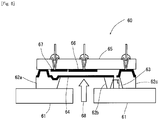
- a third embodiment of the present invention is described on the basis of Fig. 6 .
- a short silicon member 62b, a tall silicon member 62c, and a silicon member 62a that includes two flat portions respectively having the same heights as the two silicon members are disposed on lower glass 61
- a diaphragm 64 is overlaid between the silicon member 62b and the silicon member 62a in parallel with the lower glass 61
- upper glass 65 is overlaid between the silicon member 62c and the silicon member 62a in parallel with the lower glass 61
- an NEG (Non-Evaporation Getter) 63 is disposed on the lower glass 61.
- a detection electrode 66 and a reference electrode 67 are disposed on a lower surface of the upper glass 65 in a space formed by the upper glass 65 and the diaphragm 64.
- a vibrator including the graphite film of the present invention is used as the diaphragm 64 of the pressure sensor.
- the pressure sensor 60 configured as described above is capable of detecting a gas pressure 68 with a precision 10 times or more than the precision of conventional pressure sensors.
Landscapes
- Engineering & Computer Science (AREA)
- Microelectronics & Electronic Packaging (AREA)
- Manufacturing & Machinery (AREA)
- Physics & Mathematics (AREA)
- Acoustics & Sound (AREA)
- Health & Medical Sciences (AREA)
- General Health & Medical Sciences (AREA)
- Toxicology (AREA)
- Computer Hardware Design (AREA)
- Carbon And Carbon Compounds (AREA)
- Piezo-Electric Or Mechanical Vibrators, Or Delay Or Filter Circuits (AREA)
Abstract
Description
- The present invention relates to a MEMS vibrator and a MEMS oscillator each including a graphite film, and further to an electronic device such as a MEMS sensor or actuator including the MEMS oscillator.
- Oscillators are used in any electronic devices from clocks to TVs and personal computers that need a timing signal. Oscillators have been conventionally used that include a crystal vibrator generating a frequency of about 10 to 64 MHz, and oscillators (hereinafter, referred to as silicon-MEMS oscillators) are recently used that include a MEMS (Micro-electromechanical system) vibrator (hereinafter, referred to as a silicon-MEMS vibrator) including silicon as a resonator. For example, a silicon-MEMS oscillator of Si-Time Corp. has a structure combining a programmable integrated circuit (oscillator IC) with a silicon-MEMS vibrator, and a die including the oscillator IC and a die including the silicon-MEMS vibrator are sealed by wire bonding or flip-chip bonding and formed into a plastic package or a CSP (Chip-scale package). MEMS products include the silicon-MEMS oscillators as well as gyro sensors, actuators, and the like including the silicon-MEMS oscillators, and performance of the silicon-MEMS oscillators is being heightened.
- Such a conventional MEMS product has included, as a resonator (vibration source), a semiconductor material such as Si or SiGe, which is used for a mechanically vibrating portion, a spring, or the like. Si, however, has a Young's modulus of as low as 130 GPa, and further has a problem of being easily cracked. SiGe has about the same Young's modulus as Si and thus also has a problem (Non-Patent Document 1).
- Such a conventional silicon-MEMS oscillator including silicon as a resonator has a problem of mechanical characteristics and is required to be further improved also in terms of tribology, coefficient of thermal expansion characteristics, and thermal conductivity. Further, the silicon-MEMS oscillator has a problem that its vibration characteristics are largely affected by environmental temperature. In order not to allow the silicon-MEMS oscillator to be affected by temperature, the silicon-MEMS oscillator needs to be formed into a complicated structure and thus increased in stiffness.
Fig. 1 is an example of the conventional silicon-MEMS oscillator. InFig. 1 , a silicon-MEMS oscillator 10 includes asilicon substrate 11, a SiO2 layer 12, a Si layer (SOI layer: Silicon on Insulator layer) 19, a Siepitaxial layer 13, and a Poly-Si layer 18 stacked in this order, an electrostatically driven comb-shaped silicon resonator 14 is disposed so as to penetrate the Si layer (SOI layer) 19, the SiO2 layer 12 includes both end portions of the comb-shaped silicon resonator 14, and the comb-shaped silicon resonator 14 is, for the electrostatic drive, connected to an oscillator IC (not shown) including an analog oscillator circuit or the like. AMEMS terminal 16 and a CMOS (complementary metal-oxide semiconductor) 17 are disposed on the Poly-Si layer 18. As shown as an example in the drawing, the silicon-MEMS vibrator has a complicated structure and requires many processing man-hours for the production, so that it is difficult to commercialize a MEMS product that includes a vibrator having a simple both-end fixed beam structure. - As a MEMS product, an optical scanner shown in
Fig. 2 is also known that includes a Si wafer as a resonator. Anoptical scanner 20 shown as an example in the drawing includes aSi wafer 25 disposed aboveglass 24 including adetection coil 23 around X-axis and adetection coil 22 around Y-axis, theSi wafer 25 including amirror 26, a driving coil-containingrotating plate 27 around X-axis, and a driving coil-containing rotatingplate 28 around Y-axis, andpermanent magnets 21 are disposed so as to sandwich theglass 24 and form a pair. Such an optical scanner includes a Si wafer, so that it is difficult to decrease the thickness of the optical scanner. - Further, Si and other semiconductor materials are easily etched by chemicals or gasses and are inferior in chemical resistance. Therefore, when Si or other semiconductor materials are used as a resonator in the MEMS products, particularly as a diaphragm of a sensor, the purpose of use of the MEMS products (sensor) is limited. Further, when the MEMS product including Si or another semiconductor material as a resonator is used for a microchannel (micro TAS (micro Total Analysis Systems) or Lab on a Chip), the purpose of use of the MEMS products is also limited.
- On the other hand, as an example of using a carbon material for an acoustic vibrating plate, a method for baking a polymer film to prepare a graphite film has been known, and a vibrating plate and an electric acoustic transducer each including the graphite film prepared by this approach, and a method for producing the vibrating plate are proposed (Patent Document 1).
- Patent Document 1: JPH1-259698A
- Non-Patent Document 1: Shuji Tanaka, Masayoshi Esashi, Review Paper MEMS technology, Science and Industry 85 (2), 2011, pp. 49-56
- Conventional silicon-MEMS oscillators have problems of strength of a silicon resonator, chemical resistance, and the like. According to the description in EXAMPLES and the conventional art section of Patent Document 1 that uses a carbon material as an acoustic vibrating plate, use of a 50-µ m-thick polyimide as a raw material gives a graphite film having a Young's modulus of 692 GPa when treated at a highest treatment temperature of 2800° C and a graphite film having a Young's modulus of 750 GPa when treated at a highest treatment temperature of 3000° C. As pointed out by Patent
- Document 1, however, the graphite film obtained by the method of Patent Document 1 has a low mechanical strength for the use as the vibrating plate and is required to be improved in tensile strength by impregnating the graphite film with an organic polymer. Further, the vibrating plate obtained in Patent Document 1 has a thickness of at least 25 µ m or more and is too thick to be used as a MEMS vibrator.
- Therefore, an object of the present invention is to provide a MEMS vibrator that has excellent chemical resistance and an excellent mechanical strength and that is easily thinned, and an oscillator, a compact actuator, a MEMS sensor, a MEMS channel, and a micro bio reaction circuit each including the MEMS vibrator.
- In order to achieve the above purpose, the below means are used in the present invention.
- [1] A MEMS vibrator comprising:
- a vibrating film including a graphite film; and
- a silicon member supporting the vibrating film,
- the graphite film having a thickness of 50 nm or more and less than 20 µ m, and
- the graphite film having a Young's modulus along a graphite film plane direction of 700 GPa or more.
- [2] The MEMS vibrator according to [1], wherein the graphite film has a tensile strength of 50 MPa or more.
- [3] The MEMS vibrator according to [1] or [2], wherein the vibrating film is directly bonded with the silicon member.
- [4] The MEMS vibrator according to [1] or [2], wherein the vibrating film and the silicon member are bonded with each other with a metal layer.
- [5] The MEMS vibrator according to [1] or [2], wherein
the vibrating film and the silicon member are bonded with each other with a resin layer, and
the resin layer has a thickness of 0.01 µ m or more and 0.5 µ m or less. - [6] The MEMS vibrator according to any one of [1] to [3], wherein the vibrating film is bonded with the silicon member by a mechanical pressure.
- [7] An oscillator comprising:
- the MEMS vibrator according to any one of [1] to [6]; and
- an oscillator IC.
- [8] The oscillator according to [7], wherein the oscillator IC is sealed by wire bonding or flip-chip bonding.
- [9] A compact actuator comprising the oscillator according to [7] or [8].
- [10] A MEMS sensor for weighing an amount of an attached material, the MEMS sensor comprising the oscillator according to [7] or [8].
- [11] A MEMS channel comprising the MEMS vibrator according to any one of [1] to [6].
- [12] A micro bio reaction circuit comprising the MEMS vibrator according to any one of [1] to [6].
- According to the present invention, there can be provided a MEMS vibrator that has excellent chemical resistance and an excellent mechanical strength and that is easily thinned, and an oscillator, a compact actuator, a MEMS sensor, a MEMS channel, and a micro bio reaction circuit each including the MEMS vibrator. Further, a simple-structure and high-performance silicon-MLG (Multi Layer Graphene) vibrator or silicon-MLG/MEMS oscillator is obtained, and MEMS devices that are light and compact and has characteristics of chemical and gas resistance are provided such as a high-sensitivity MEMS sensor or actuator that include the oscillator.
-
-
Fig. 1 is a diagram showing one example of a conventional silicon-MEMS oscillator. -
Fig. 2 is a diagram showing one example of a conventional optical scanner including a Si wafer as a resonator. -
Fig. 3 is diagrams each showing one example of a method for bonding a graphite film of the present invention with a silicon member supporting the film by a mechanical pressure. -
Fig. 4 is diagrams each showing one example of a high-precision MEMS vibrator including a graphite film of the present invention. -
Fig. 5 is diagrams each showing one example of an actuator including a graphite film of the present invention. -
Fig. 6 is a diagram showing one example of a pressure sensor including a graphite film of the present invention. - A MEMS vibrator of the present invention is a graphite-MEMS vibrator having a graphite film as a resonator, specifically a MEMS vibrator that includes a vibrating film including a graphite film, and a silicon member supporting the vibrating film, and the present invention is characterized in that the graphite film has a thickness of 50 nm or more and less than 20 µ m and a Young's modulus along a graphite film plane direction of 700 GPa or more.
- The graphite film of the present invention exerts a high Young' s modulus, a high density, and a high tensile strength as a polymer film having a prescribed thickness is baked at a high temperature and graphite is thus uniformly formed across the entire film.
- The thickness of the graphite film is determined according to handleability of the graphite film and ease of preparing a device, and is less than 20 µ m, preferably 18 µ m or less, more preferably 16 µ m or less, most preferably 15 µ m or less. The graphite film in such a range is capable of reducing the weight of graphite having a small specific gravity (for example, 2.24). The values of the Young' s modulus, the tensile strength, and the electrical conductivity tend to increase as the thickness of the graphite film is decreased.
- Further, the graphite film has a thickness of 50 nm or more, preferably 80 nm or more, more preferably 100 nm or more, most preferably 200 nm or more. The graphite film having a thickness of 50 nm or more becomes capable of transmitting, as a resonator, prescribed vibration to the exterior.
- A graphene ribbon having about a single to 10 layers has a thickness of no more than about 0.34 nm to 3.4 nm and has no function as a resonator. Further, it is difficult for a CVD method to prepare multilayer graphene having mechanical characteristics necessary as a resonator when the thickness is set at 50 nm or more.
- A method for measuring the thickness can be performed using a known device. For example, the thickness can be measured by a contact measurement method with a caliper or the like, by an optical measurement method with a laser displacement meter, spectroscopic ellipsometry, or the like, or by a section observation method with an SEM (Scanning Electron Microscope) or a TEM (Transmission Electron Microscope).
- The graphite film has an elasticity (Young's modulus) along the graphite film plane direction of 700 GPa or more. The graphite film has an elasticity along the graphite film plane direction of preferably 800 GPa or more, most preferably 900 GPa or more. The graphite film has an elasticity along the graphite film plane direction of, for example, 1500 GPa or less, preferably 1100 GPa or less. These values of the Young's modulus are remarkably higher than the values of commercially available graphite products and are remarkably higher than the values of aluminum (Young's modulus: 70.3 GPa), copper (Young's modulus: 129.8 GPa), beryllium (Young's modulus: 287 GPa), and mica (Young's modulus: 210 GPa). Further, the highest value of the Young's modulus of a conventional graphite crystal is 1020 GPa, and the present invention also targets a graphite film exceeding the highest value.
- The Young's modulus of the graphite film becomes high as graphite is increased in quality and as the heat treatment temperature for graphitization is increased. The young's modulus of 700 GPa or more is achieved by a heat treatment temperature of about 2800° C.
- The graphite film of the present invention may have a smaller Young's modulus along a graphite film thickness direction than the Young' s modulus of the graphite vibrating plate described in Patent Document 1, but preferably has a mechanical strength of a prescribed Young' s modulus or more along the graphite film thickness direction. The graphite film of the present invention preferably has a Young' s modulus (Ec) along the graphite film thickness direction of preferably 40 GPa or more, more preferably 50 GPa or more and, for example, 500 GPa or less. A graphite single crystal has a Young's modulus (Ea) along a basal plane (a-b plane) direction of 1020 GPa, while having a Young's modulus (Ec) along a c-axis direction of about 36 GPa and being inferior in the Young's modulus along the thickness direction.
- The Young' s moduli along the graphite film thickness direction and the graphite film plane direction of the graphite film of the present invention are obtained by a conventionally known method, and can be obtained by, for example, a stationary test such as a tensile test (test piece: JIS G05567J II-6, measurement device: Autograph universal testing machine AG-IS manufactured by SHIMADZU CORPORATION), a compression test, or a torsion test, or a dynamic test such as a resonance method (test piece: JIS Z2280, measurement device: high-temperature Young's modulus measurement device EG-HT/JE manufactured by Nihon Techno-Plus Corp.), an ultrasonic pulse method (test piece: JIS Z2280, measurement device: burst wave acoustic velocity measurement device RAM-5000 manufactured by RITEC Inc.), or a pendulum method.
- Particularly, a resonance method, in which a resonance frequency (characteristic vibration frequency) is measured by applying mechanically or electrically forced vibration to a test piece and a Young's modulus of the graphite film is calculated from the resonance, can be preferably used. In the present invention, a free resonance method which is the most general among resonance methods is mainly used. This method requires the test piece to be electrically conductive, and the graphite film has an excellent electrical conductivity. From such a viewpoint, the resonance method is preferably used.
- The graphite film has a density of, for example, more than 2.1 g/cm3, preferably 2.15 g/cm3 or more, more preferably 2.17 g/cm3 or more, further preferably 2.20 g/cm3 or more. The graphite film has a density of, for example, 2.24 g/cm3 or less. As the graphite film has a higher density, air or voids included in the film are decreased to easily increase the film strength (for example, tensile strength).
- The graphite film of the present invention has an excellent mechanical strength and is stably capable of achieving a value of the tensile strength in the range of, for example, 50 to 100 MPa, preferably about 60 to 100 MPa, more preferably about 70 to 100 MPa. Therefore, the graphite film is singly capable of constituting a vibrating film, which means that the graphite film is capable of forming a vibrating film without impairing the excellent characteristics of the graphite film.
- The tensile strength can be obtained by, for example, a method described in JIS K 7127 or ASTM D882.
- The graphite film has an electrical conductivity of preferably 15000 S/cm or more, more preferably 17000 S/cm or more, further preferably 19000 S/cm or more. The graphite film has an electrical conductivity of preferably 27000 S/cm or less, more preferably 26000 S/cm or less. The electrical conductivity can be calculated from an electrical resistance measured by a known approach such as the van Der Pauw method or a general four-terminal method, and dimensions and a thickness of the sample.
- Further, the graphite film has a surface roughness Ra of preferably less than 15 µ m, more preferably 10 µ m or less, further preferably 8 µ m or less, further more preferably 5 µ m or less. The lower limit is not particularly limited but may be, for example, 0.1 µ m. The surface roughness of the graphite film is adjustable by applying a pressure during graphitization, or performing carbonization and/or graphitization while applying a tension from the exterior. The pressure applied during graphitization may be set at, for example, 80 kgf/cm2 to 130 kgf/cm2.
- A method for producing the graphite film is not particularly limited as long as the graphite film satisfies the conditions of the mechanical characteristics and the thickness, but a preferable method is a polymer baking method in which a polymer film is heat-treated to graphitize the polymer film.
- A raw material polymer used in the polymer baking method is an aromatic polymer such as an aromatic polyimide, a polyamide, polyparaphenylene vinylene, polyoxadiazole, polybenzimidazole, or polybenzoxazole. Among these aromatic polymers, an aromatic polyimide is particularly preferable.
- In an approach for carbonizing and graphitizing an aromatic polyimide, a polymer film as a starting material is heated and carbonized in an inert gas. As the inert gas, nitrogen, argon, or a mixed gas of argon and nitrogen is preferably used. The carbonization is usually performed at a temperature of about 500° C to 1000° C. The polyimide film is thermally decomposed at nearly 500 to 600° C and becomes a carbonized film formed of almost only carbon at nearly 1000° C.
- A graphitization reaction is performed in an inert gas and is most appropriately performed in an argon gas.
- When the aromatic polyimide is used, the thickness of the aromatic polyimide is preferably 100 nm to 40 µm, more preferably 100 nm to 20 µm, most preferably 100 nm to 10 µm. The aromatic polyimide becomes almost half in thickness by the carbonization described above and the graphitization described below, so that the use of the aromatic polyimide having the thickness described above gives the graphite film having the objective thickness.
- Meanwhile, the thickness of the graphite film obtained by a conventional polymer baking method is 20 µm or more. A reason why the graphite film that is produced by the polymer baking method and has a thickness of less than 20 µm is not commercialized is that it is difficult to establish a production process achieving a thickness of less than 20 µm. General polymer baking methods generate many wrinkles in a process of carbonization or graphitization and remarkably cause generation of wrinkles when a thickness of the graphite film becomes less than 20 µm. The present invention is capable of preventing the generation of wrinkles by carbonizing an aromatic polyimide film or graphitizing a carbonized film of the aromatic polyimide film while applying a tension to the film, or by graphitizing the carbonized film under pressure, and is capable of giving a film having a thickness of less than 20 µm.
- In the present invention, necessary temperature (highest treatment temperature) for graphitization is 2800° C or more. The treatment may be performed at a temperature of 2900° C or more, 3000° C or more and 3300° C or less, as necessary. With the graphitization at 2800° C or more, the graphite film having a film thickness of the present invention is capable of achieving the prescribed Young' s modulus and tensile strength. The retention time at the highest treatment temperature is, for example, 10 minutes or more, preferably 30 minutes or more and may be 1 hour or more. The upper limit of the retention time at the highest treatment temperature is not particularly limited, but may be usually 5 hours or less, particularly about 3 hours or less.
- When a pressure is applied during graphitization, the ambient pressure (gauge pressure) by an inert gas in a high-temperature furnace is, for example, 0.01 MPa or more, preferably 0.02 MPa or more, further preferably 0.05 MPa or more. The upper limit of the ambient pressure is not particularly limited but may be, for example, 2 MPa or less, particularly about 1.8 MPa or less.
- In the present invention, in order to suppress wrinkles, it is recommended that a tensile stress be applied to the aromatic polyimide film or the carbonized film during carbonization or graphitization, or the carbonized film be graphitized under pressure, as described above.
- The graphite film obtained by the method described above has characteristics of being less affected by environmental temperature due to the treatment at 2800° C or more, and can be formed into a graphite resonator having both necessary thickness and high mechanical physical properties. The graphite resonator is useful for preparing a graphite-MEMS vibrator (particularly a broadband vibrator), and gives a high frequency resonance characteristics due to particularly having a high Young' s modulus.
- Hereinafter, the MEMS vibrator of the present invention is described with reference to examples shown in drawings.
- The MEMS vibrator includes a vibrating film including the graphite film, and a silicon member (hereinafter, sometimes referred to as a silicon support) supporting the vibrating film, and the vibrating film is preferably bonded with the silicon support. In the bonding of the vibrating film with the silicon support, the graphite film needs to be bonded with the silicon support along a graphite film a-b plane. The bonding of the graphite film a-b plane with a silicon surface is preferably performed by direct bonding without an adhesive material, bonding with a metal layer or a resin layer, or contact bonding with a mechanical pressure.
- The direct bonding of the graphite film a-b plane with the silicon surface without an adhesive material is the most excellent bonding method taking advantage of graphite characteristics. For the direct bonding, a mirror-finished graphite surface obtained by polishing may be compression-bonded with a mirrored silicon surface at normal temperature. In this procedure, the graphite surface and the silicon surface can each be surface-treated in vacuum and thus activated to achieve strong direct bonding. For the activation, there can be preferably used, for example, a method for activating the surfaces by an argon beam in vacuum and a method for activating the surfaces by a FAB gun.
- The bonding of the graphite film a-b plane with the silicon surface is also achieved by a soldering method using a metal. The soldering is a technique in which a metal is melted by heat to be flowed into a gap between objects to be bonded and the objects are bonded by interdiffusion between the solder material and a base material. An alloy having a lower melting point than the melting points of members to be bonded can be melted and used as a kind of adhesive to bond the plurality of members without melting base materials themselves of the members.
- The graphite film a-b plane and the silicon surface may be bonded with each other with a resin layer, and the resin layer has a thickness of preferably 0.01 µm or more and 0.5 µm or less, more preferably 0.02 µm or more, further preferably 0.05 µm or more.
- The resin layer may be an acrylic adhesive, an epoxy adhesive, or the like. A general adhesive, such as an epoxy adhesive, that is soft is preferably used with a thickness of 1 µm or less so as not to impair the excellent mechanical characteristics of the graphite film.
- The graphite film a-b plane may be bonded with the silicon surface by applying a mechanical pressure.
Fig. 3 shows one example of such bonding. InFig. 3(a) , agraphite film 31 is overlaid across asilicon support 32 having agroove 32a. A method for fixing thegraphite film 31 between thesilicon support 32 and ametal jig 33 is indicated. In the method, themetal jig 33 that has fourcolumns 36 and has a U shape in a front view is put into thesilicon support 32 on one of contact surfaces between thegraphite film 31 and thesilicon support 32, while allowing themetal jig 33 to straddle thegraphite film 31. Thecolumns 36 of themetal jig 33 are made from a metal, a carbon material, or silicon, inserted into holes provided on thesilicon support 32, and can be fixed by pressing a rear surface of themetal jig 33. - On the other hand,
Fig. 3(b) shows a method for overlaying agraphite film 31 across asilicon support 32 that has agroove 32a, and adjusting a tension of thegraphite film 31 by compression-bonding thegraphite film 31 with ametal jig 33 on one of contact surfaces between thegraphite film 31 and thesilicon support 32. Apiezoelectric element 34 is fitted to a side of a base 32b of one end of thesilicon support 32 to be sandwiched, and the tension is adjustable by expanding or contracting thepiezoelectric element 34. The tension is also adjustable by disposing an electrostatic actuator or the like in the side of the base 32b of the one end. - The MEMS vibrator obtained described above constitutes an oscillator (MEMS oscillator) together with an oscillator IC.
- The oscillator IC may be sealed by wire bonding or flip-chip bonding.
- The MEMS vibrator of the present invention is applicable to an information communication field including an optical scanner and an optical micro encoder, a sensor field including various sensors such as an infrared sensor, an acceleration sensor, and a pressure sensor, a medical and bio field including a microprobe of a scanning microscope, a DNA chip, a micro reactor, and a medical flexible tube, and MEMS products such as a head of an inkjet printer, a micro pump, and a compact actuator.
- Among these application examples, the MEMS vibrator and the MEMS oscillator are preferably used in a compact actuator, preferably used in a MEMS sensor for weighing the amount of an attached material, and preferably used in a MEMS channel or a micro bio reaction circuit.
- The present application claims a benefit of priority based on Japanese Patent Application No.
2018-036682 filed on March 1, 2018 2018-036682 filed on March 1, 2018 - Heretofore, a basic production process for preparing a silicon MEMS element using a graphite film has been described. Hereinafter, a device prepared using such a process is described with reference to examples.
- The thicknesses of a polyimide film as a polymer film and a graphite film had a margin of error of about ±5% depending on the measurement location of the films in the form of a film (sheet). Therefore, a ten-point average thickness of a resultant sheet was defined as the thickness of the sample in the present invention.
- The electrical conductivity of the graphite film was measured by the van Der Pauw method. This method is the most appropriate method for measuring the electrical conductivity of a sample in the form of a thin film. The details of the measurement method is described in Experimental chemistry 9 (fourth series) electricity and magnetism (edited by The Chemical Society of Japan, issued by Maruzen Co., Ltd., (issued on June 5, 1991 (Heisei 3)) p.170. This method is characterized in that electrodes can be arranged in any four points of end portions in a thin film sample having any shape, to measure the electrical conductivity and that accurate measurement can be performed when the sample has a uniform thickness. In the present invention, the measurement was performed by using a 2 cm x 2 cm sample and attaching a silver paste electrode to each of four corners of the sample. The measurement was performed using Resistivity/DC & AC Hall measurement system, ResiTest 8300 manufactured by TOYO Corporation.
- The Young's modulus was measured by a free resonance method. This is a method for mechanically or electrically applying forced vibration to a test piece, measuring a resonance frequency (characteristic vibration frequency), and calculating a Young' s modulus of the graphite film from the resonance frequency.
- The tensile strength is measured on the basis of ASTM D882.
- The graphite film was cut out into a size of 2 x 16 cm, and the cut-out film was reinforced at both ends with a 12.5-µm-thick polyimide tape. The measurement sample prepared was set in a vertical motorized test stand (EMX-1000N manufactured by IMADA CO., LTD.). The tensile speed was set at 5 mm/min, and the tensile strength was measured by a digital force gauge (ZTA-5N manufactured by IMADA CO., LTD.).
- A raw material polyimide film was prepared by the following method. Into 100 g of a 18% by mass DMF solution of polyamic acid synthesized from pyromellitic anhydride and 4,4' -diaminodiphenyl ether in the mole ratio of 1 : 1, a curing agent formed of 20 g of acetic anhydride and 10 g of isoquinoline was mixed, and the mixture was stirred, defoamed by centrifugal separation, then applied by casting onto an aluminum foil, and further a polyamic acid film having a uniform thickness in the range of 40 µm or less was prepared on the aluminum foil using a spin coater. The thickness of the film was adjusted by changing the concentration of the amid acid solution and the number of rotations. The polyamic acid film was heated at 120° C for 150 seconds and at 300° C, 400° C, and 500° C for 30 seconds each, and then the aluminum foil was removed. Thus, polyimide films having different thicknesses were prepared.
- The polyimide films having different thicknesses were carbonized by raising the temperature to 1000° C at a rate of 10° C/min in a nitrogen gas with use of an electric furnace and keeping the temperature at 1000° C for 1 hour. Next, the resultant carbonized films were set in a graphitization furnace, and the temperature was raised to 3200° C at a heating rate of 20° C/min in an argon atmosphere under a pressure of 0.10 MPa (1.0 kg/cm2). The temperature was retained at 3200° C for 30 minutes and thereafter lowered at a rate of 40° C/min to prepare graphite films. In the preparation, the thickness of the eventually obtained graphite films was approximately half the thickness of the raw material polyimide films. The resultant graphite films were films in which graphite layers were oriented in parallel with a graphite film plane direction and were highly oriented.
- For use of the graphite film of the present invention as a vibrating film, the wrinkles generated in the carbonization and graphitization processes are preferably reduced. The reduction of the wrinkles in the carbonization process and the graphitization process was achieved by a flattening technique of graphitization under pressure and a flattening technique of baking while giving a tension. The graphitization under pressure is a method for simultaneously graphitizing a plurality of samples under pressure, while preventing the bonding between the samples. For example, the graphitization without pressure gave a surface roughness Ra value of 15 µm, whereas the graphitization under a pressure of 100 kgf could reduce the Ra value to as small as 5 to 3 µm. The tension baking method is a method for performing carbonization or graphitization while applying tension from the exterior. The samples with few wrinkle (Ra = 0.5 µm) was prepared by this method.
- The thickness, the electrical conductivity (S/cm), the Young's modulus (GPa) along the graphite film plane direction, and the value (MPa) of the tensile strength of the resultant graphite films are shown below. The value of the tensile strength is an average value of 10 samples obtained by measuring 12 samples cut out into a strip (width 2 cm,
length 16 cm) and excluding the values of 2 samples that exhibited the minimum values. A reason why such measurement was performed is that the value of the tensile strength derives from a small scratch on a cut surface and such a sample is considered not to exhibit an accurate film strength. - (G1) Thickness: 14.2 µm, electrical conductivity: 21000 S/cm, Young's modulus: 780 GPa, tensile strength: 56 MPa
- (G2) Thickness: 4.6 µm, electrical conductivity: 23900 S/cm, Young's modulus: 870 GPa, tensile strength: 62 MPa
- (G3) Thickness: 2.0 µ m, electrical conductivity: 24300 S/cm, Young's modulus: 1020 GPa, tensile strength: 86 MPa
- (G4) Thickness: 1.2 µm, electrical conductivity: 21500 S/cm, Young's modulus: 970 GPa, tensile strength: 94 MPa
- (G5) Thickness: 0.72 µm, electrical conductivity: 22000 S/cm, Young's modulus: 860 GPa, tensile strength: 96 MPa
- (G6) Thickness: 0.24 µm, electrical conductivity: 21000 S/cm, Young's modulus: 800 GPa, tensile strength: 90 MPa
- (G7) Thickness: 0.06 µm, electrical conductivity: 20200 S/cm, Young's modulus: 720 GPa, tensile strength: 82 MPa
- A first embodiment according to the present invention is described on the basis of
Fig. 4. Fig. 4(a) shows a high-precision MEMS vibrator 40 prepared by overlaying agraphite film 41 with a thickness of 50 nm or more and less than 20 µm across asilicon support 42 with twobase portions 42b, and fixing thebase portions 42b and thegraphite film 41 by a bond between thebase portions 42b and thegraphite film 41 with a metal such as silver solder or with a uniformly applied resin such as a resist of submicron order, or through pressure bonding such as crimping. In theMEMS vibrator 40, thegraphite film 41 is vibrated by applying vibration to one or both of thebase portions 42b from a piezoelectric film (not illustrated) such as PZT. The vibration of thegraphite film 41 can be detected by an electrostatic signal between thegraphite film 41 and an electrode (not illustrated) disposed on an upper portion of thegraphite film 41. - The resonance frequency of the
MEMS vibrator 40 is 6 GHz when thegraphite film 41 having a width of 5 µm and a length of 5 µm is used, and theMEMS vibrator 40 is capable of generating higher-frequency vibration than the resonance frequency (1.8 GHz) provided when a silicon resonator having the same size as thegraphite film 41 is used. Further, as shown inFig. 4(b) , aweight 43 movable in a wave propagation direction can be disposed on a surface of thegraphite film 41 to freely change the resonance frequency. - A second embodiment of the present invention is described on the basis of
Fig. 5 . In an example ofFig. 5(a) , a high-stiffness compact actuator 50 was prepared by forming, on abase portion 52b of asilicon support 52, a composite that includes apiezoelectric film 54 and agraphite film 51 of the present invention in this order. In an example ofFig. 5(b) , astacked body 58 including a graphite film is fixed at fourpoints 59, and when a moving electrode or a fixed electrode is disposed, thestacked body 58 moves opposite to a prescribedacceleration direction 56 and the electrostatic capacitance progresses in an electrostaticcapacitance progressing direction 57. The graphite film of the present invention can be utilized as a structural material of a spring with high-stiffness. - A third embodiment of the present invention is described on the basis of
Fig. 6 . Specifically, in apressure sensor 60 illustrated as an example in the drawing, ashort silicon member 62b, atall silicon member 62c, and asilicon member 62a that includes two flat portions respectively having the same heights as the two silicon members are disposed onlower glass 61, adiaphragm 64 is overlaid between thesilicon member 62b and thesilicon member 62a in parallel with thelower glass 61,upper glass 65 is overlaid between thesilicon member 62c and thesilicon member 62a in parallel with thelower glass 61, and an NEG (Non-Evaporation Getter) 63 is disposed on thelower glass 61. Adetection electrode 66 and areference electrode 67 are disposed on a lower surface of theupper glass 65 in a space formed by theupper glass 65 and thediaphragm 64. In this example, a vibrator including the graphite film of the present invention is used as thediaphragm 64 of the pressure sensor. Thepressure sensor 60 configured as described above is capable of detecting agas pressure 68 with aprecision 10 times or more than the precision of conventional pressure sensors. -
- 10
- Silicon-MEMS oscillator
- 11
- Silicon substrate
- 12
- SiO2 layer
- 13
- Si epitaxial layer
- 14
- Comb-shaped silicon resonator
- 15
- Enlarged portion
- 16
- MEMS terminal
- 17
- CMOS
- 18
- Poly-Si layer
- 19
- Si layer (SOI layer: Silicon on Insulator layer)
- 20
- Optical scanner
- 21
- Permanent magnet
- 22
- Detection coil around Y-axis
- 23
- Detection coil around X-axis
- 24
- Glass
- 25
- Si wafer
- 26
- Mirror
- 27
- Rotating plate around X-axis
- 28
- Rotating plate around Y-axis
- 31, 41, 51
- Graphite film
- 32
- Silicon support
- 33
- Metal jig
- 34
- Piezoelectric element
- 40
- MEMS vibrator
- 42
- Silicon support
- 43
- Weight
- 50
- Actuator
- 52
- Silicon support
- 52b
- Base portion
- 54
- Piezoelectric film
- 56
- Acceleration direction
- 57
- Electrostatic capacitance progressing direction
- 60
- Pressure sensor
- 61, 65
- Glass
- 62a, 62b, 62c
- Silicon member
- 63
- NEG (Non-Evaporation Getter)
- 64
- Diaphragm
- 66
- Detection electrode
- 67
- Reference electrode
- 68
- Gas pressure
Claims (12)
- A MEMS vibrator comprising:a vibrating film including a graphite film; anda silicon member supporting the vibrating film,the graphite film having a thickness of 50 nm or more and less than 20 µm, andthe graphite film having a Young's modulus along a graphite film plane direction of 700 GPa or more.
- The MEMS vibrator according to claim 1, wherein the graphite film has a tensile strength of 50 MPa or more.
- The MEMS vibrator according to claim 1 or 2, wherein the vibrating film is directly bonded with the silicon member.
- The MEMS vibrator according to claim 1 or 2, wherein the vibrating film and the silicon member are bonded with each other with a metal layer.
- The MEMS vibrator according to claim 1 or 2, wherein
the vibrating film and the silicon member are bonded with each other with a resin layer, and
the resin layer has a thickness of 0.01 µm or more and 0.5 µm or less. - The MEMS vibrator according to any one of claims 1 to 3, wherein the vibrating film is bonded with the silicon member by a mechanical pressure.
- An oscillator comprising:the MEMS vibrator according to any one of claims 1 to 6; andan oscillator IC.
- The oscillator according to claim 7, wherein the oscillator IC is sealed by wire bonding or flip-chip bonding.
- A compact actuator comprising the oscillator according to claim 7 or 8.
- A MEMS sensor for weighing an amount of an attached material, the MEMS sensor comprising the oscillator according to claim 7 or 8.
- A MEMS channel comprising the MEMS vibrator according to any one of claims 1 to 6.
- A micro bio reaction circuit comprising the MEMS vibrator according to any one of claims 1 to 6.
Applications Claiming Priority (2)
| Application Number | Priority Date | Filing Date | Title |
|---|---|---|---|
| JP2018036682 | 2018-03-01 | ||
| PCT/JP2019/007003 WO2019167865A1 (en) | 2018-03-01 | 2019-02-25 | Mems vibrator and mems oscillator |
Publications (2)
| Publication Number | Publication Date |
|---|---|
| EP3761505A1 true EP3761505A1 (en) | 2021-01-06 |
| EP3761505A4 EP3761505A4 (en) | 2021-12-01 |
Family
ID=67805031
Family Applications (1)
| Application Number | Title | Priority Date | Filing Date |
|---|---|---|---|
| EP19760832.6A Pending EP3761505A4 (en) | 2018-03-01 | 2019-02-25 | Mems vibrator and mems oscillator |
Country Status (4)
| Country | Link |
|---|---|
| US (1) | US11655145B2 (en) |
| EP (1) | EP3761505A4 (en) |
| JP (1) | JP7340514B2 (en) |
| WO (1) | WO2019167865A1 (en) |
Cited By (1)
| Publication number | Priority date | Publication date | Assignee | Title |
|---|---|---|---|---|
| US11835539B2 (en) | 2019-10-17 | 2023-12-05 | Valqua, Ltd. | Low heat-resistant sensor |
Families Citing this family (1)
| Publication number | Priority date | Publication date | Assignee | Title |
|---|---|---|---|---|
| CN113678379B (en) * | 2019-04-30 | 2022-08-30 | 金泰克斯公司 | Vehicle trainable transceiver with programmable oscillator |
Family Cites Families (20)
| Publication number | Priority date | Publication date | Assignee | Title |
|---|---|---|---|---|
| JPH01259698A (en) | 1988-04-08 | 1989-10-17 | Res Dev Corp Of Japan | Diaphragm electric acoustic converter and manufacture of diaphragm |
| US5178804A (en) * | 1990-07-27 | 1993-01-12 | Matsushita Electric Industrial Co., Ltd. | Method of manufacturing acoustic diaphragm |
| US5658698A (en) | 1994-01-31 | 1997-08-19 | Canon Kabushiki Kaisha | Microstructure, process for manufacturing thereof and devices incorporating the same |
| JP3181174B2 (en) * | 1994-06-08 | 2001-07-03 | キヤノン株式会社 | Method of forming microstructure |
| JP4076792B2 (en) | 2001-06-19 | 2008-04-16 | 独立行政法人科学技術振興機構 | Cantilever array, manufacturing method and apparatus |
| JP4231228B2 (en) * | 2002-01-21 | 2009-02-25 | 株式会社リコー | Micromachine |
| KR100613398B1 (en) * | 2003-11-25 | 2006-08-17 | 한국과학기술연구원 | Cantilever sensor type analysis system, manufacturing method and ultrafine material detection method using the same |
| CN100570429C (en) * | 2004-06-24 | 2009-12-16 | 康乃尔研究基金会有限公司 | MEMS optical scanner based on fiber composite material |
| JP5135628B2 (en) * | 2007-08-31 | 2013-02-06 | セイコーインスツル株式会社 | Oscillator and oscillator using the same |
| JP5322173B2 (en) * | 2009-09-07 | 2013-10-23 | 国立大学法人 宮崎大学 | Formation method of fine channel |
| US8980217B2 (en) * | 2010-12-21 | 2015-03-17 | Nec Corporation | Method of manufacturing graphene substrate, and graphene substrate |
| JP2012150350A (en) * | 2011-01-20 | 2012-08-09 | Ricoh Co Ltd | Functional element package, optical scanner, image forming apparatus, and packaging method for functional element package |
| JP5586067B2 (en) * | 2011-05-18 | 2014-09-10 | 日本電信電話株式会社 | Micromechanical vibrator and manufacturing method thereof |
| US20130062104A1 (en) * | 2011-09-08 | 2013-03-14 | Cornell University - Cornell Center For Technology Enterprise & Commercialization (Cctec) | Resonant material layer apparatus, method and applications |
| JP6060569B2 (en) * | 2012-09-07 | 2017-01-18 | セイコーエプソン株式会社 | Manufacturing method of electronic device |
| EP3007206A4 (en) * | 2013-05-24 | 2017-03-15 | Mitsui Chemicals, Inc. | Pellicle and euv exposure device comprising same |
| JP6699146B2 (en) * | 2015-12-02 | 2020-05-27 | 凸版印刷株式会社 | Imprint method |
| JP2018036682A (en) | 2016-08-29 | 2018-03-08 | 日本電産サンキョー株式会社 | Card processor |
| US10823630B1 (en) * | 2016-11-11 | 2020-11-03 | Iowa State University Research Foundation, Inc. | High sensitivity MEMS pressure sensor |
| JP2018125696A (en) * | 2017-01-31 | 2018-08-09 | 太陽誘電株式会社 | Piezoelectric thin film resonator, filter and multiplexer |
-
2019
- 2019-02-25 WO PCT/JP2019/007003 patent/WO2019167865A1/en not_active Ceased
- 2019-02-25 EP EP19760832.6A patent/EP3761505A4/en active Pending
- 2019-02-25 JP JP2020503483A patent/JP7340514B2/en active Active
-
2020
- 2020-08-31 US US17/007,891 patent/US11655145B2/en active Active
Cited By (1)
| Publication number | Priority date | Publication date | Assignee | Title |
|---|---|---|---|---|
| US11835539B2 (en) | 2019-10-17 | 2023-12-05 | Valqua, Ltd. | Low heat-resistant sensor |
Also Published As
| Publication number | Publication date |
|---|---|
| WO2019167865A1 (en) | 2019-09-06 |
| US20200399120A1 (en) | 2020-12-24 |
| US11655145B2 (en) | 2023-05-23 |
| JP7340514B2 (en) | 2023-09-07 |
| JPWO2019167865A1 (en) | 2021-02-12 |
| EP3761505A4 (en) | 2021-12-01 |
Similar Documents
| Publication | Publication Date | Title |
|---|---|---|
| CN105659495B (en) | Piezo-electric resonator and its manufacturing method | |
| US8307521B2 (en) | Method for manufacturing acceleration sensing unit | |
| US11655145B2 (en) | MEMS vibrator and MEMS oscillator | |
| JP5778914B2 (en) | Method for manufacturing electromechanical transducer | |
| JP7218134B2 (en) | CAPACITIVE TRANSDUCER AND MANUFACTURING METHOD THEREOF | |
| JP3465675B2 (en) | Piezoelectric / electrostrictive film type element | |
| Karuthedath et al. | Development of ScAlN PMUTs for medical applications | |
| US7126255B2 (en) | Piezoelectric/electrostrictive film-type device | |
| JP3706903B2 (en) | Flexible high sensitivity ceramic sensor | |
| JP6488667B2 (en) | Surface acoustic wave device | |
| EP2001062A9 (en) | Membrane structure element and method for manufacturing same | |
| US9444403B2 (en) | Resonation element, resonator, oscillator, electronic device and moving object | |
| JP6786796B2 (en) | Electronic devices, methods of manufacturing electronic devices, electronic devices and mobiles | |
| JPH08107219A (en) | Semiconductor acceleration sensor and its manufacture | |
| Wang et al. | Design and fabrication of piezoelectrically driven deformable reflective micromirrors based on MEMS technology | |
| JP3986944B2 (en) | Excitation sensor | |
| JP4736315B2 (en) | Piezoelectric element and manufacturing method thereof | |
| Sharma et al. | Reliability Study of MEMS Piezoelectric Sensing Structure | |
| JPH08116101A (en) | Piezoelectric element and manufacturing method thereof | |
| CN117388048A (en) | A low-dimensional material strain control testing device and its preparation method | |
| CN121185413A (en) | A flexible capacitive accelerometer for vibration monitoring of hydropower units and its fabrication method | |
| Davis | Investigation of Residual and Thermal Stress on Membrane-Based MEMS Devices | |
| Bespalova | Development of piezoelectric microelectromechanical systems for multiaxial motion and sensing | |
| JP2001185737A (en) | Manufacturing method of acceleration sensor | |
| JP2021164130A (en) | Vibrating piece, electronic device, and moving object |
Legal Events
| Date | Code | Title | Description |
|---|---|---|---|
| STAA | Information on the status of an ep patent application or granted ep patent |
Free format text: STATUS: THE INTERNATIONAL PUBLICATION HAS BEEN MADE |
|
| PUAI | Public reference made under article 153(3) epc to a published international application that has entered the european phase |
Free format text: ORIGINAL CODE: 0009012 |
|
| STAA | Information on the status of an ep patent application or granted ep patent |
Free format text: STATUS: REQUEST FOR EXAMINATION WAS MADE |
|
| 17P | Request for examination filed |
Effective date: 20200907 |
|
| AK | Designated contracting states |
Kind code of ref document: A1 Designated state(s): AL AT BE BG CH CY CZ DE DK EE ES FI FR GB GR HR HU IE IS IT LI LT LU LV MC MK MT NL NO PL PT RO RS SE SI SK SM TR |
|
| AX | Request for extension of the european patent |
Extension state: BA ME |
|
| DAV | Request for validation of the european patent (deleted) | ||
| DAX | Request for extension of the european patent (deleted) | ||
| A4 | Supplementary search report drawn up and despatched |
Effective date: 20211028 |
|
| RIC1 | Information provided on ipc code assigned before grant |
Ipc: B81C 1/00 20060101ALN20211022BHEP Ipc: B81B 7/00 20060101ALN20211022BHEP Ipc: H03H 3/02 20060101ALN20211022BHEP Ipc: H03H 9/02 20060101ALN20211022BHEP Ipc: H03H 3/007 20060101ALI20211022BHEP Ipc: H03H 9/24 20060101AFI20211022BHEP |
|
| STAA | Information on the status of an ep patent application or granted ep patent |
Free format text: STATUS: EXAMINATION IS IN PROGRESS |
|
| 17Q | First examination report despatched |
Effective date: 20231130 |