EP3761259A1 - Electronic device - Google Patents
Electronic device Download PDFInfo
- Publication number
- EP3761259A1 EP3761259A1 EP18907901.5A EP18907901A EP3761259A1 EP 3761259 A1 EP3761259 A1 EP 3761259A1 EP 18907901 A EP18907901 A EP 18907901A EP 3761259 A1 EP3761259 A1 EP 3761259A1
- Authority
- EP
- European Patent Office
- Prior art keywords
- light
- electronic device
- imaging
- transparent
- section
- Prior art date
- Legal status (The legal status is an assumption and is not a legal conclusion. Google has not performed a legal analysis and makes no representation as to the accuracy of the status listed.)
- Pending
Links
Images










Classifications
-
- G—PHYSICS
- G06—COMPUTING OR CALCULATING; COUNTING
- G06F—ELECTRIC DIGITAL DATA PROCESSING
- G06F1/00—Details not covered by groups G06F3/00 - G06F13/00 and G06F21/00
- G06F1/16—Constructional details or arrangements
- G06F1/1613—Constructional details or arrangements for portable computers
- G06F1/1633—Constructional details or arrangements of portable computers not specific to the type of enclosures covered by groups G06F1/1615 - G06F1/1626
- G06F1/1684—Constructional details or arrangements related to integrated I/O peripherals not covered by groups G06F1/1635 - G06F1/1675
- G06F1/1686—Constructional details or arrangements related to integrated I/O peripherals not covered by groups G06F1/1635 - G06F1/1675 the I/O peripheral being an integrated camera
-
- A—HUMAN NECESSITIES
- A61—MEDICAL OR VETERINARY SCIENCE; HYGIENE
- A61B—DIAGNOSIS; SURGERY; IDENTIFICATION
- A61B5/00—Measuring for diagnostic purposes; Identification of persons
- A61B5/117—Identification of persons
- A61B5/1171—Identification of persons based on the shapes or appearances of their bodies or parts thereof
- A61B5/1172—Identification of persons based on the shapes or appearances of their bodies or parts thereof using fingerprinting
-
- G—PHYSICS
- G06—COMPUTING OR CALCULATING; COUNTING
- G06F—ELECTRIC DIGITAL DATA PROCESSING
- G06F3/00—Input arrangements for transferring data to be processed into a form capable of being handled by the computer; Output arrangements for transferring data from processing unit to output unit, e.g. interface arrangements
- G06F3/01—Input arrangements or combined input and output arrangements for interaction between user and computer
- G06F3/03—Arrangements for converting the position or the displacement of a member into a coded form
- G06F3/041—Digitisers, e.g. for touch screens or touch pads, characterised by the transducing means
-
- A—HUMAN NECESSITIES
- A61—MEDICAL OR VETERINARY SCIENCE; HYGIENE
- A61B—DIAGNOSIS; SURGERY; IDENTIFICATION
- A61B5/00—Measuring for diagnostic purposes; Identification of persons
- A61B5/0059—Measuring for diagnostic purposes; Identification of persons using light, e.g. diagnosis by transillumination, diascopy, fluorescence
- A61B5/0077—Devices for viewing the surface of the body, e.g. camera, magnifying lens
-
- G—PHYSICS
- G02—OPTICS
- G02B—OPTICAL ELEMENTS, SYSTEMS OR APPARATUS
- G02B6/00—Light guides; Structural details of arrangements comprising light guides and other optical elements, e.g. couplings
- G02B6/0001—Light guides; Structural details of arrangements comprising light guides and other optical elements, e.g. couplings specially adapted for lighting devices or systems
- G02B6/0011—Light guides; Structural details of arrangements comprising light guides and other optical elements, e.g. couplings specially adapted for lighting devices or systems the light guides being planar or of plate-like form
- G02B6/0013—Means for improving the coupling-in of light from the light source into the light guide
- G02B6/0023—Means for improving the coupling-in of light from the light source into the light guide provided by one optical element, or plurality thereof, placed between the light guide and the light source, or around the light source
- G02B6/0028—Light guide, e.g. taper
-
- G—PHYSICS
- G02—OPTICS
- G02B—OPTICAL ELEMENTS, SYSTEMS OR APPARATUS
- G02B6/00—Light guides; Structural details of arrangements comprising light guides and other optical elements, e.g. couplings
- G02B6/0001—Light guides; Structural details of arrangements comprising light guides and other optical elements, e.g. couplings specially adapted for lighting devices or systems
- G02B6/0011—Light guides; Structural details of arrangements comprising light guides and other optical elements, e.g. couplings specially adapted for lighting devices or systems the light guides being planar or of plate-like form
- G02B6/0013—Means for improving the coupling-in of light from the light source into the light guide
- G02B6/0023—Means for improving the coupling-in of light from the light source into the light guide provided by one optical element, or plurality thereof, placed between the light guide and the light source, or around the light source
- G02B6/003—Lens or lenticular sheet or layer
-
- G—PHYSICS
- G06—COMPUTING OR CALCULATING; COUNTING
- G06F—ELECTRIC DIGITAL DATA PROCESSING
- G06F1/00—Details not covered by groups G06F3/00 - G06F13/00 and G06F21/00
- G06F1/16—Constructional details or arrangements
- G06F1/1613—Constructional details or arrangements for portable computers
- G06F1/163—Wearable computers, e.g. on a belt
-
- G—PHYSICS
- G06—COMPUTING OR CALCULATING; COUNTING
- G06F—ELECTRIC DIGITAL DATA PROCESSING
- G06F21/00—Security arrangements for protecting computers, components thereof, programs or data against unauthorised activity
- G06F21/30—Authentication, i.e. establishing the identity or authorisation of security principals
- G06F21/31—User authentication
- G06F21/32—User authentication using biometric data, e.g. fingerprints, iris scans or voiceprints
-
- G—PHYSICS
- G06—COMPUTING OR CALCULATING; COUNTING
- G06F—ELECTRIC DIGITAL DATA PROCESSING
- G06F3/00—Input arrangements for transferring data to be processed into a form capable of being handled by the computer; Output arrangements for transferring data from processing unit to output unit, e.g. interface arrangements
- G06F3/01—Input arrangements or combined input and output arrangements for interaction between user and computer
- G06F3/03—Arrangements for converting the position or the displacement of a member into a coded form
- G06F3/041—Digitisers, e.g. for touch screens or touch pads, characterised by the transducing means
- G06F3/0412—Digitisers structurally integrated in a display
-
- G—PHYSICS
- G06—COMPUTING OR CALCULATING; COUNTING
- G06F—ELECTRIC DIGITAL DATA PROCESSING
- G06F3/00—Input arrangements for transferring data to be processed into a form capable of being handled by the computer; Output arrangements for transferring data from processing unit to output unit, e.g. interface arrangements
- G06F3/01—Input arrangements or combined input and output arrangements for interaction between user and computer
- G06F3/03—Arrangements for converting the position or the displacement of a member into a coded form
- G06F3/041—Digitisers, e.g. for touch screens or touch pads, characterised by the transducing means
- G06F3/044—Digitisers, e.g. for touch screens or touch pads, characterised by the transducing means by capacitive means
-
- G—PHYSICS
- G06—COMPUTING OR CALCULATING; COUNTING
- G06V—IMAGE OR VIDEO RECOGNITION OR UNDERSTANDING
- G06V10/00—Arrangements for image or video recognition or understanding
- G06V10/10—Image acquisition
- G06V10/17—Image acquisition using hand-held instruments
-
- G—PHYSICS
- G06—COMPUTING OR CALCULATING; COUNTING
- G06V—IMAGE OR VIDEO RECOGNITION OR UNDERSTANDING
- G06V30/00—Character recognition; Recognising digital ink; Document-oriented image-based pattern recognition
- G06V30/10—Character recognition
- G06V30/14—Image acquisition
- G06V30/142—Image acquisition using hand-held instruments; Constructional details of the instruments
-
- G—PHYSICS
- G06—COMPUTING OR CALCULATING; COUNTING
- G06V—IMAGE OR VIDEO RECOGNITION OR UNDERSTANDING
- G06V40/00—Recognition of biometric, human-related or animal-related patterns in image or video data
- G06V40/10—Human or animal bodies, e.g. vehicle occupants or pedestrians; Body parts, e.g. hands
- G06V40/12—Fingerprints or palmprints
- G06V40/13—Sensors therefor
-
- G—PHYSICS
- G06—COMPUTING OR CALCULATING; COUNTING
- G06V—IMAGE OR VIDEO RECOGNITION OR UNDERSTANDING
- G06V40/00—Recognition of biometric, human-related or animal-related patterns in image or video data
- G06V40/10—Human or animal bodies, e.g. vehicle occupants or pedestrians; Body parts, e.g. hands
- G06V40/12—Fingerprints or palmprints
- G06V40/13—Sensors therefor
- G06V40/1306—Sensors therefor non-optical, e.g. ultrasonic or capacitive sensing
-
- H—ELECTRICITY
- H04—ELECTRIC COMMUNICATION TECHNIQUE
- H04N—PICTORIAL COMMUNICATION, e.g. TELEVISION
- H04N23/00—Cameras or camera modules comprising electronic image sensors; Control thereof
-
- H—ELECTRICITY
- H04—ELECTRIC COMMUNICATION TECHNIQUE
- H04N—PICTORIAL COMMUNICATION, e.g. TELEVISION
- H04N23/00—Cameras or camera modules comprising electronic image sensors; Control thereof
- H04N23/50—Constructional details
-
- H—ELECTRICITY
- H10—SEMICONDUCTOR DEVICES; ELECTRIC SOLID-STATE DEVICES NOT OTHERWISE PROVIDED FOR
- H10K—ORGANIC ELECTRIC SOLID-STATE DEVICES
- H10K59/00—Integrated devices, or assemblies of multiple devices, comprising at least one organic light-emitting element covered by group H10K50/00
- H10K59/40—OLEDs integrated with touch screens
-
- H—ELECTRICITY
- H10—SEMICONDUCTOR DEVICES; ELECTRIC SOLID-STATE DEVICES NOT OTHERWISE PROVIDED FOR
- H10K—ORGANIC ELECTRIC SOLID-STATE DEVICES
- H10K59/00—Integrated devices, or assemblies of multiple devices, comprising at least one organic light-emitting element covered by group H10K50/00
- H10K59/60—OLEDs integrated with inorganic light-sensitive elements, e.g. with inorganic solar cells or inorganic photodiodes
- H10K59/65—OLEDs integrated with inorganic image sensors
-
- G—PHYSICS
- G06—COMPUTING OR CALCULATING; COUNTING
- G06F—ELECTRIC DIGITAL DATA PROCESSING
- G06F2203/00—Indexing scheme relating to G06F3/00 - G06F3/048
- G06F2203/041—Indexing scheme relating to G06F3/041 - G06F3/045
- G06F2203/04109—FTIR in optical digitiser, i.e. touch detection by frustrating the total internal reflection within an optical waveguide due to changes of optical properties or deformation at the touch location
-
- G—PHYSICS
- G06—COMPUTING OR CALCULATING; COUNTING
- G06F—ELECTRIC DIGITAL DATA PROCESSING
- G06F2203/00—Indexing scheme relating to G06F3/00 - G06F3/048
- G06F2203/041—Indexing scheme relating to G06F3/041 - G06F3/045
- G06F2203/04112—Electrode mesh in capacitive digitiser: electrode for touch sensing is formed of a mesh of very fine, normally metallic, interconnected lines that are almost invisible to see. This provides a quite large but transparent electrode surface, without need for ITO or similar transparent conductive material
-
- G—PHYSICS
- G06—COMPUTING OR CALCULATING; COUNTING
- G06F—ELECTRIC DIGITAL DATA PROCESSING
- G06F3/00—Input arrangements for transferring data to be processed into a form capable of being handled by the computer; Output arrangements for transferring data from processing unit to output unit, e.g. interface arrangements
- G06F3/01—Input arrangements or combined input and output arrangements for interaction between user and computer
- G06F3/03—Arrangements for converting the position or the displacement of a member into a coded form
- G06F3/041—Digitisers, e.g. for touch screens or touch pads, characterised by the transducing means
- G06F3/0416—Control or interface arrangements specially adapted for digitisers
- G06F3/04164—Connections between sensors and controllers, e.g. routing lines between electrodes and connection pads
-
- G—PHYSICS
- G06—COMPUTING OR CALCULATING; COUNTING
- G06F—ELECTRIC DIGITAL DATA PROCESSING
- G06F3/00—Input arrangements for transferring data to be processed into a form capable of being handled by the computer; Output arrangements for transferring data from processing unit to output unit, e.g. interface arrangements
- G06F3/01—Input arrangements or combined input and output arrangements for interaction between user and computer
- G06F3/03—Arrangements for converting the position or the displacement of a member into a coded form
- G06F3/041—Digitisers, e.g. for touch screens or touch pads, characterised by the transducing means
- G06F3/044—Digitisers, e.g. for touch screens or touch pads, characterised by the transducing means by capacitive means
- G06F3/0446—Digitisers, e.g. for touch screens or touch pads, characterised by the transducing means by capacitive means using a grid-like structure of electrodes in at least two directions, e.g. using row and column electrodes
-
- H—ELECTRICITY
- H10—SEMICONDUCTOR DEVICES; ELECTRIC SOLID-STATE DEVICES NOT OTHERWISE PROVIDED FOR
- H10K—ORGANIC ELECTRIC SOLID-STATE DEVICES
- H10K2102/00—Constructional details relating to the organic devices covered by this subclass
- H10K2102/301—Details of OLEDs
- H10K2102/302—Details of OLEDs of OLED structures
- H10K2102/3023—Direction of light emission
- H10K2102/3031—Two-side emission, e.g. transparent OLEDs [TOLED]
Definitions
- the present disclosure relates to an electronic device having an imaging function.
- Example of a device that performs biometric authentication includes a fingerprint sensor device that performs fingerprint authentication by imaging a surface of a finger.
- a wristband-type small electronic device for example, has recently been developed.
- a fingerprint authentication function it is desirable to implement, in a small electronic device, a plurality of functions such as a displaying function and an imaging function, but in some cases, it is difficult to implement desired functions due to a limited surface area. Further, in a case where a fingerprint authentication function is to be implemented, it may be difficult, in a small electronic device, for a fingerprint sensor device to bring a finger to an optimal position.
- An electronic device includes a transparent panel section in which a plurality of transparent light-emitting elements is disposed, and an imaging section that is disposed under a partial region of the transparent panel section, and images, via the transparent panel section, an object which is in contact with or in proximity to the partial region of the transparent panel section.
- the object which is in contact with or in proximity to the partial region of the transparent panel section is imaged by the imaging section disposed under the partial region of the transparent panel section.
- an electronic device is applicable to various types of information terminals and the like, an example will be given in which the technology of the present disclosure is applied to a wristband-type electronic device as one example in the present embodiment.
- FIG. 1 schematically illustrates a configuration example of an electronic device 1 according to a first embodiment of the present disclosure.
- the electronic device 1 includes a wristband body 2 having a ring shape, a transparent panel section 10 and an imaging section 20 provided on a portion of the wristband body 2, and a cover glass 3 provided on an upper surface of the transparent panel section 10.
- the cover glass 3 and a panel section-valid region 11 of the transparent panel section 10 may each be transparent as a whole.
- the transparent panel section 10 includes a plurality of transparent light-emitting elements 16 arranged in a matrix as illustrated in FIG. 7 , which will be described later, a plurality of wiring lines for light-emitting elements coupled to the respective plurality of transparent light-emitting elements 16, and a lattice-shaped structural member 70 that separates the plurality of transparent light-emitting elements 16 from each other.
- the transparent light-emitting element 16 includes, for example, a transparent organic EL (Electro Luminescence) element (transparent OLED (Organic Light Emitting Diode)).
- the transparent light-emitting element 16 may also be a quantum dot light-emitting element.
- the transparent panel section 10 has a function as a display panel for displaying an image on the panel section-valid region 11 using light emitted by the plurality of transparent light-emitting elements 16. Further, the transparent panel section 10 has a function as a touch sensor for detecting a touch state of an object such as a finger or the like on the basis of a value of capacitance between the plurality of wiring lines for light-emitting elements, for example.
- the imaging section 20 is disposed under a partial region of the transparent panel section 10.
- the imaging section 20 has a function of imaging, via the transparent panel section 10, an object which is in contact with or in proximity to the partial region of the transparent panel section 10.
- the object to be imaged by the imaging section 20 may be, for example, a portion of a living body.
- the imaging section 20 may have a function of a biometric authentication device that performs biometric authentication on a part of a living body on the basis of a captured image of the part of the living body obtained by imaging the part of the living body.
- the function as the biometric authentication device of the imaging section 20 enables a configuration of a fingerprint sensor, for example,
- FIG. 2 illustrates a display example of the transparent panel section 10 included in the electronic device 1.
- the transparent panel section 10 includes, for example, the panel section-valid region 11 that displays various types of information as illustrated in FIG. 2 .
- the various types of information display may be various shapes and various types of text information.
- the transparent panel section 10 displays a message indicating performing "personal authentication" in a case where the imaging section 20 is used as a fingerprint sensor, information promoting placing of a finger at a position corresponding to the imaging section 20, and the like.
- FIGs. 3 and 4 each illustrate a main structure of the electronic device 1.
- FIG. 3 illustrates a structure of the transparent panel section 10 and a vicinity thereof when the electronic device 1 is viewed from upper side (side of an object to be imaged).
- FIG. 4 corresponds to a cross-section taken along a line A-A in FIGs. 1 and 3 .
- FIG. 5 illustrates a detailed configuration example of the imaging section 20.
- the transparent panel section 10 includes the panel section-valid region 11, a panel section-outer frame 12, and a panel driver 13.
- the electronic device 1 further includes a touch determination section 14 and a light emission controller 15 coupled to the transparent panel section 10.
- a plurality of transparent light-emitting elements 16 is arranged in a matrix.
- the touch determination section 14 determines, in a case where the transparent panel section 10 is used as a touch sensor, a state of a touch.
- the light emission controller 15 controls light emission of the plurality of transparent light-emitting elements 16 via the panel driver 13.
- the imaging section 20 includes a microlens array module 21, an imaging section-outer frame 22, an imaging element 30, and a substrate 31.
- the microlens array module 21 is disposed within the panel section-valid region 11 of the transparent panel section 10 as viewed from the upper side.
- the electronic device 1 further includes an imaging processor 32 coupled to the imaging element 30 and an authentication processor 33 coupled to the imaging processor 32.
- the imaging element 30 includes, for example, a CMOS (Complementary Metal Oxide Semiconductor) sensor.
- the imaging element 30 is disposed on the substrate 31.
- the imaging processor 32 performs predetermined image processing on a captured image obtained by the imaging element 30.
- the authentication processor 33 performs biometric authentication on the basis of the captured image that has been subjected to the image processing by the imaging processor 32.
- the authentication processor 33 performs, for example, in a case where the imaging section 20 is used as a fingerprint sensor, a process of fingerprint authentication.
- the authentication processor 33 authenticates a fingerprint pattern, for example, as the process of the fingerprint authentication.
- minutiae ridge ending and bifurcation of a fingerprint
- the authentication processor 33 may authenticate feature amounts of sweat glands or veins instead of the fingerprint as the biometric authentication.
- authentication may be performed by combining two or more feature amounts among the feature amounts of the fingerprint, the sweat glands, and the veins.
- the microlens array module 21 is disposed between the imaging element 30 and the panel section-valid region 11 of the transparent panel section 10.
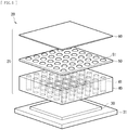
- the microlens array module 21 includes, in order from the upper side, a cover glass-and-light guide plate 60, a microlens array 50, and a light guide plate 40.
- the microlens array 50 includes a plurality of microlenses 51 arranged in a matrix.
- the microlens array 50 collects object light from an object such as a finger or the like toward the imaging element 30 by each of the plurality of microlenses 51.
- the cover glass-and-light guide plate 60 serves to protect a surface of the microlens array 50.
- the cover glass-and-light guide plate 60 has a function of bringing the object light transmitted through the panel section-valid region 11 of the transparent panel section 10 to each of the plurality of microlenses 51.
- the cover glass-and-light guide plate 60 has a plurality of light guide paths each provided at corresponding one of positions of the plurality of microlenses 51.
- the light guide plate 40 has a plurality of light guide paths 41.
- the plurality of light guide paths 41 is each provided at corresponding one of the positions of the plurality of microlenses 51, and brings the light collected by each of the plurality of microlenses 51 to the imaging element 30.
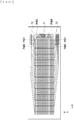
- FIG. 6 illustrates an example of regions to be imaged by the microlenses 51 of the imaging section 20.
- FIG. 7 illustrates an exmaple of a relationship between a structure of the transparent panel section 10 and disposition positions of the microlenses 51 of the imaging section 20.
- FIG. 8 schematically illustrates object images 34 formed on the imaging element 30 of the imaging section 20.
- FIG. 9 illustrates an example of a captured image 35 by obtained by the imaging section 20 and a post-compositing process image 36 based on the captured image 35.
- the transparent panel section 10 includes the plurality of wiring lines for light-emitting elements coupled to the respective plurality of transparent light-emitting elements 16 arranged in a matrix, and the lattice-shaped structural member 70 that separates the plurality of transparent light-emitting elements 16 from each other.
- the plurality of microlenses 51 be disposed to cause the plurality of microlenses 51 not to overlap with the lattice-shaped structural member 70 as viewed from the upper side (object side), to cause the lattice-shaped structural member 70 not to be shown in the captured image.
- the plurality of microlenses 51 may be disposed to cause an arrangement pitch p2 of the plurality of microlenses 51 to be substantially the same as an arrangement pitch p1 of the plurality of transparent light-emitting elements 16.
- a plurality of image portions corresponding to the arrangement pitch p2 of the plurality of microlenses 51 is formed as object images 34 on the imaging element 30 of the imaging section 20. Consequently, as illustrated in FIG. 9 , a plurality of partial images is formed as the captured image 35.
- the imaging processor 32 as illustrated in FIG. 9 , the plurality of partial image in the captured image 35 is subjected to a compositing process to generate the post-compositing process image 36. This generates a whole image of the object.
- the imaging section 20 is preferably configured in a manner that imaging regions (light-capturing areas) of adjacent plurality of microlenses 51 with respect to the object (a finger 90) to be imaged are partially overlapped, as illustrated in FIG. 6 .
- the plurality of partial images whose peripheral portions partially overlap each other is formed as the captured image 35; therefore, in a case where the compositing process is performed as illustrated in FIG. 9 , it is possible to generate a seamless whole image without conspicuous seams.
- FIG. 10 illustrates a first modification example of a structure of the transparent panel section 10 and disposition positions of the microlenses 51 of the imaging section 20.
- the plurality of microlenses 51 be disposed so as not to overlap with the lattice-shaped structural member 70 as viewed from the upper side (object side), to cause the lattice-shaped structural member 70 not to be shown in the captured image.
- the microlenses 51 may overlap with the lattice-shaped structural member 70 as viewed from the upper side (object side) as illustrated in FIG. 10 , and the lattice-shaped structural member 70 may be shown in the captured image. In such a case, it is desirable to perform image processing to cause the image of the lattice-shaped structural member 70 to be erased by the imaging processor 32.
- the process of the biometric authentication may also be performed on the basis of the captured image in which the image of the lattice-shaped structural member 70 remains to be shown, without performing the image processing of erasing the image of the lattice-shaped structural member 70.
- it is possible to increase the accuracy of the biometric authentication by performing the process of the biometric authentication using a statistical method on the captured image in which the lattice-shaped structural member 70 remains to be shown, for example.
- data to be used for the process of the statistical biometric authentication may be acquired from a database or the like stored in an external server or the like.
- the transparent panel section 10 When imaging by the imaging section 20 is performed, the transparent panel section 10 may be caused to emit light to be used as illumination light for imaging.
- the transparent panel section 10 causes a transparent light-emitting element 16 disposed at a position different from at least a position at which a microlens 16 to be used for the imaging is disposed, as viewed from the object side, among the plurality of transparent light-emitting elements 16 disposed in a partial region corresponding to the imaging section 20, to emit light for illumination, when the imaging by the imaging section 20 is performed.
- FIG. 11 illustrates a second modification example of a relationship between a structure of the transparent panel section 10 and disposition positions of the microlenses 51 of the imaging section 20. Further, FIG. 11 illustrates an example of a light emitting state of the transparent panel section 11 at a time of imaging.
- the plurality of microlenses 51 may be disposed to cause the arrangement pitch p2 of the plurality of microlenses 51 to be greater than the arrangement pitch p1 of the plurality of transparent light-emitting elements 16.
- the plurality of microlenses 51 is disposed to cause the arrangement pitch p2 to be twice the arrangement pitch p1 of the plurality of transparent light-emitting elements 16.
- the plurality of microlenses 51 is disposed to cause the arrangement pitch p2 to be an integral multiple of two or more of the arrangement pitch p1 of the plurality of transparent light-emitting elements 16.
- the transparent panel section 10 may cause a transparent light-emitting element 16 disposed at a position different from at least a position at which a microlens 16 to be used for the imaging is disposed, as viewed from the object side, among the plurality of transparent light-emitting elements 16 disposed in the partial region corresponding to the imaging section 20, to emit light for illumination.
- FIG. 12 shows a third modification example of the relation between the structure of transparent panel section 10 and disposition position of microlenses 51 of imaging section 20.
- FIG. 12 is a third modification example of a relationship between a configuration of the transparent panel section 10 and disposition positions of the microlenses 51 of the imaging section 20. Further, FIG. 12 illustrates an example of a light emitting state of the transparent panel section 11 at a time of imaging.
- a transparent light-emitting element 17 having a segmented structure for illumination may be disposed at an outside of a region in which the plurality of microlenses 16 is disposed, as viewed from the object side.
- the transparent panel section 10 may cause a transparent light-emitting element 17 having the segmented structure for illumination disposed at a position different from at least a position at which a microlens 16 to be used for the imaging is disposed among the plurality of transparent light-emitting elements 16 to emit light.
- FIG. 13 illustrates an example of a wiring structure of the transparent panel section 10.
- FIG. 14 illustrates an implementation example of a touch sensor function using wiring lines of the transparent panel section 10.
- the transparent panel section 10 includes, as the plurality of wiring lines for light-emitting elements, a plurality of common lines 71 to which a common drive signal is supplied and a plurality of segment lines 72 to which an individual drive signal is supplied.
- the plurality of common lines 71 extends in a first direction and is arranged in a second direction that intersects the first direction.
- the plurality of common lines 71 is coupled to the respective plurality of transparent light-emitting elements 16 in the first direction.
- the first direction is a horizontal direction (a direction parallel to a left/right direction and an X direction)
- the second direction is a vertical direction (a direction parallel to a top/bottom direction and a Y direction).
- the plurality of segment lines 72 extends in the second direction and is arranged in the first direction.
- the plurality of segment lines 72 is coupled to the respective plurality of transparent light-emitting elements 16 in the second direction.
- One end or the other end of the plurality of segment lines 72 is pulled out so as to alternately extend to the upper right side or the lower right side in the horizontal direction.
- the plurality of segment lines 72 may be divided approximately into halves of left and right portions, and a first electrode section (PAD1) may be coupled to one end side of each of the plurality of segment lines 72 included in the left half portion.
- a second electrode section (PAD2) may be coupled to one end side of each of the plurality of common lines 71 included in the right half potion.
- the plurality of common lines 71 may be divided approximately into halves of top and bottom portions, and a third electrode section (PAD3) may be coupled to one end side of each of the plurality of common lines 71 included in the top half portion.
- a fourth electrode section (PAD4) may be coupled to one end side of each of the plurality of common lines 71 included in the bottom half portion.
- FIG. 14 it is possible to form two sensor regions in the horizontal direction and two sensor regions in the vertical direction, a total of four sensor regions (four channels) in the top, bottom, left, and right. That is, it is possible to form: a sensor region of the first electrode section (PAD1) and the third electrode section (PAD3); a sensor region of the first electrode section (PAD1) and the fourth electrode section (PAD4); a sensor region of the second electrode section (PAD2) and the third electrode section (PAD3); and a sensor region of the second electrode section (PAD2) and the fourth electrode section (PAD4).
- the common line 71 corresponds to a specific example of a "first wiring line” according to the present disclosure.
- the segment line 72 corresponds to a specific example of a "second wiring line” according to the present disclosure.
- the touch determination section 14 is able to determine a state of touch in the transparent panel section 10 on the basis of a value of capacitance between at least one wiring line out of the plurality of first wiring lines and at least one wiring line out of the plurality of second wiring lines. For example, in the example of FIG.
- the number into which the sensor region is to be divided is not limited to four, and may be three or less, or five or more.
- the direction in which the sensor region is divided is not limited to two directions, and may be only one direction. For example, as illustrated in FIG. 18 , which will be described later, it may have a structure such that there are four sensor regions (four channels) in the horizontal direction.
- the plurality of common lines 71 and the plurality of segment lines 72 both serve as the wiring lines for light-emitting elements and the wiring lines for touch detection has been described as an example in the above explanation; however, the plurality of common lines 71 and the plurality of segment lines 72 may be provided as the wiring lines for touch detection different from the wiring lines for the light-emitting elements.
- the plurality of wiring lines for light-emitting elements and the plurality of wiring lines for touch detection may be provided inside a single transparent panel section 10, or the transparent panel section 10 may have a structure in which a panel for light emission (for display) including the plurality of wiring lines for light-emitting elements and a panel for touch detection including the plurality of wiring lines for touch detection are stacked.
- a touch sensor (the transparent panel section 10) in the electronic device 1
- FIG. 15 is a configuration example of a control system of the electronic device 1 for performing calibration of the touch sensor.
- the electronic device 1 includes the transparent panel section 10 serving as the touch sensor, the imaging section 20 serving as the fingerprint sensor, a CPU (Central Processing Unit) 110, a storage 113, and a communication section 114.
- the CPU 110 has a function as a controller 111 and a function as a determination section 112.
- the function as the controller 111 and the function as the determination section 112 may be achieved as a program (software) to be executed by the CPU 110, or may be achieved as functions built in at least one of the transparent panel section 10 and the imaging section 20.
- the CPU 110 may have the functions of the touch determination section 14 and the light emission controller 15 described above ( FIG. 3 ), and the functions of the imaging processor 32 and the authentication processor 33.
- the determination section 112 may include the function of the touch determination section 14.
- the communication section 114 performs data communication to and from the server 115 via a wireless or wired network.
- the control parameter of touch detection includes, for example, a determination threshold of a touch state and a working interval of the touch sensor.
- control parameters methods of achieving calibration of the determination threshold of the touch state and calibration of the working interval of the touch sensor will be described.
- capacitance measured by the touch sensor As for capacitance measured by the touch sensor, a larger value is measured as an area being in contact is larger when touched.
- capacitance measured by the touch sensor may vary depending on a person who performs touching or an environment. Appropriate correction (calibration) is necessary to accurately determine the touch state without such human variations or environmental variations.
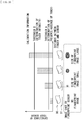
- FIG. 16 illustrates an outline of determination thresholds of touch states in the electronic device 1.
- FIG. 16 illustrates how thresholds for determining touch states are decided by combining the fingerprint sensor and the touch sensor.
- the upper part of FIG. 16 illustrates a relationship between capacitance (vertical axis) measured by the touch sensor and a distance (horizontal axis) between a finger 90 and a sensor surface 91 of the touch sensor.
- the lower part of FIG. 16 illustrates shot images of the fingerprint sensor corresponding to the distances between the finger 90 and the sensor surface 91 of the touch sensor.
- the thresholds of the value of capacitance for determining a presence or absence of the touch (threshold A) and an intensity of the touch (threshold B) on the basis of the relationship between the size (area) of the fingerprint image shot by the fingerprint sensor and the value of capacitance measured by the touch sensor.
- the determination section 112 determines the state of the touch in the touch sensor on the basis of at least one determination threshold. Further, the determination section 112 determines, as the state of the touch, at least the presence or absence of the touch and the intensity of the touch.
- the controller 111 has a function as a determination threshold calculation section that calculates at least one determination threshold on the basis of the value of capacitance in the touch sensor and a captured image of an object imaged by the imaging section 20 (the fingerprint image shot by the fingerprint sensor).
- the determination threshold calculation section calculates, as the at least one determination threshold, at least a first determination threshold (threshold A in FIG. 16 ) to be used for the determination of the presence or absence of the touch, and a second determination threshold (threshold B in FIG. 16 ) to be used for the determination of the intensity of the touch.
- controller 111 and the determination section 112 for performing calibration of the determination threshold of the touch state may be achieved as functions built in at least one of the transparent panel section 10 and the imaging section 20.
- Parameter information such as the calculated determination threshold may be stored in the storage 113 or may be stored in the server 120 by the communication section 114.
- FIG. 17 illustrates an outline of a process of calculating a determination threshold of a touch state in the electronic device 1.
- a value of capacitance is acquired by the touch sensor (step S101), and at the same time, a fingerprint image is shot by the fingerprint sensor (step S102).
- the electronic device 1 determines a pattern of the shot image (step S103).
- the state of the touch is estimated from an image size of the finger 90 that has been shot. For example, in a case where the electronic device 1 determines that the pattern is "no fingerprint image" in step S103, the electronic device 1 determines that the state is no touch (step S104). In a case where the electronic device 1 determines that the pattern is "fingerprint image: small” in step S103, the electronic device 1 determines that the state is a light touch (step S105). Further, in a case where the electronic device 1 determines that the pattern is "fingerprint image size: large” in step S103, the electronic device 1 determines that the state is a strong touch (step S106).
- step S107 determines whether data necessary for deciding the determination threshold of the touch state has been acquired. If the electronic device 1 determines that the necessary data has not been acquired (step S107: N), the electronic device 1 returns to step S101.
- step S107 determines that the necessary data has been acquired by repeating the process of acquiring the necessary data as described above (step S107: Y)
- the electronic device 1 calculates the determination threshold of the touch state on the basis of the data of the relationship between the value of capacitance of the touch sensor and the state of the touch (step S108), and ends the process.
- a moving speed of the finger 90 and a time period of being in contact when performing touching are different for each user.
- a fast operation causes missing of data if the working interval of touch detection is long, resulting in a malfunction.
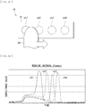
- the touch sensor has four sensor channels, ch1, ch2, ch3, and ch4.
- FIG. 18 illustrates an example of an operation of the user on the touch sensor in the electronic device 1.
- FIG. 19 illustrates a first example of change in values of capacitance with time detected by the touch sensor in the electronic device 1.
- FIG. 20 illustrates a second example of change in values of capacitance with time detected by the touch sensor in the electronic device 1.
- FIG. 19 is a graph where the working interval of the touch sensor is 8 msec, and it can be confirmed that the peaks of the values of capacitance in the respective channels sequentially appear as the finger 90 is moved.
- FIG. 20 is a graph where the working interval of the touch sensor is 30 msec.
- the peak of the sensor channel ch3 is not confirmed. This occurs because the working interval of the touch sensor is long and a temporal resolution is low, and thereby causing missing of data when the finger 90 passes through the sensor channel ch3.
- the following describes a method of, by combining the fingerprint sensor and the touch sensor, identifying a user by the fingerprint sensor and determining the optimal working interval of the touch sensor on the basis of an operation history (statistical data of the operation speeds) of the user.
- the controller 111 controls the working interval of touch detection in the touch sensor on the basis of a result of authentication performed by the authentication processor 33 ( FIG. 3 ).
- the controller 111 acquires a statistic of an operation speed of the touch of the user authenticated by the authentication processor 33 ( FIG. 3 ), on the basis of a database related to the operation speed in which a plurality of users to be subjected to the biometric authentication by the authentication processor 33 are associated with statistics of operation speeds of touches in the touch sensor by the respective plurality of users.
- the controller 111 calculates a working interval of touch detection optimized for the authenticated user on the basis of the acquired statistic of the operation speed of the touch.
- Parameter data for each user including the operation speed and the database related to the operation speed may be stored in the storage 113 or acquired from the server 120 by the communication section 114.
- controller 111 for performing calibration of the working interval of the touch sensor may be achieved as functions built in at least one of the transparent panel section 10 and the imaging section 20.
- FIG. 21 illustrates an outline of a process of correcting a working interval of the touch sensor in the electronic device 1.
- the electronic device 1 performs fingerprint authentication (step S201) and identifies a fingerprint pattern of a user (step S202).
- the electronic device 1 reads out and acquires from the database a statistic related to the operation speed corresponding to the identified fingerprint pattern (steps S203, S204, and S205). It is to be noted that, although FIG. 21 illustrates an operation example in a case where the fingerprint pattern is selected from three patterns A, B, and C for the sake of explanation, the number of fingerprint patterns to be selected is not limited to three, and may be any number.
- the electronic device 1 calculates the optimal working interval of the touch sensor for the user on the basis of the acquired statistic (step S206). Thereafter, the electronic device 1 changes the working interval of the touch sensor to the calculated value and ends the process (step S207).
- FIG. 22 illustrates an example of a database of statistics related to operation speeds of users in the electronic device 1 created from operation histories of the users.
- FIG. 22 includes, as examples of operation speed parameters for calculating the working interval of the touch sensor, a sliding speed indicating a speed at which the finger 90 is moved laterally, and a touching speed indicating a speed at which the finger 90 is touched and released.
- FIG. 22 illustrates an example in the case where the fingerprint patterns are three patterns A, B, and C
- the number of fingerprint patterns registered in the database is not limited to three, and may be any number.
- the imaging section 20 that images, via the transparent panel section 10, the object (the finger 90) which is in contact with or in proximity to the partial region of the transparent panel section 10 is disposed under the partial region of the transparent panel section 10; therefore, it is possible to achieve a plurality of functions in a compact size.
- the display function and the touch sensor function may be achieved by the transparent panel section 10
- the imaging function for fingerprint authentication may be achieved by the imaging section 20.
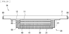
- FIGs. 23 and 24 each illustrate a main structure of an electronic device 1A according to the second embodiment of the present disclosure.
- FIG. 23 illustrates a structure of the transparent panel section 10 and a vicinity thereof when the electronic device 1A is viewed from the upper side (the side of an object to be imaged).
- FIG. 24 corresponds to a cross-section taken along a line A-A in FIG. 23 .
- the example (refer to FIGs. 11 and 12 ) has been given in which the transparent panel section 10 is partially caused to emit light to be used as the illumination light for imaging when imaging is performed by the imaging section 20; however, as illustrated in FIGs. 23 and 24 , an illumination light source 80 for imaging may be separately provided.
- the illumination light source 80 may be, for example, an LED (Light Emitting Diode).
- the illumination light source 80 is disposed at an outside of a partial region (a region corresponding to the imaging section 20) of the transparent panel section 10.
- the illumination light source 80 may be disposed on at least one side surface of the cover glass 3 provided on the upper side of the transparent panel section 10, for example.
- the illumination light sources 80 are respectively disposed on two opposite sides of the cover glass 3.
- the illumination light may be emitted by the illumination light sources 80.
- the illumination light source 80 and the partial light emission by the transparent panel section 10 may be used in combination.
- FIG. 25 illustrates a main structure of an electronic device 1B according to the third embodiment of the present disclosure.
- FIG. 25 illustrates a structure of the transparent panel section 10 and a vicinity thereof when the electronic device 1B is viewed from the upper side (the side of an object to be imaged).
- the panel section-valid region 11 of the transparent panel section 10 is transparent as a whole; therefore, underlying structures of the panel section-valid region 11 may be visible when the transparent panel section 10 is not emitting light. For this reason, a design material 18 may be disposed under the transparent panel section 10 as illustrated in FIG. 25 .
- the design material 18 may have a wood-grain pattern or any pattern, for example. As a result, it is possible to improve a design property.
- the design material 18 is desirably disposed under a region different from the partial region of the transparent panel section 10 (the region corresponding to the imaging section 20) as viewed from the upper side, so as not to affect the imaging of the object performed by the imaging section 20. Further, the design material 18 is desirably disposed under at least a region corresponding to the panel section-valid region 11 other than the region corresponding to the imaging section 20 as viewed from the upper side.
- the present disclosure may have the following configurations.
- the imaging section that images, via the transparent panel section, the object which is in contact with or in proximity to the partial region of the transparent panel section is disposed under the partial region of the transparent panel section; therefore, it is possible to achieve a plurality of functions in a compact size.
- the display function and the touch sensor function may be achieved by the transparent panel section, and the imaging function for fingerprint authentication may be achieved by the imaging section.
Landscapes
- Engineering & Computer Science (AREA)
- Physics & Mathematics (AREA)
- Theoretical Computer Science (AREA)
- General Physics & Mathematics (AREA)
- Life Sciences & Earth Sciences (AREA)
- General Engineering & Computer Science (AREA)
- Health & Medical Sciences (AREA)
- Multimedia (AREA)
- Human Computer Interaction (AREA)
- Inorganic Chemistry (AREA)
- Chemical & Material Sciences (AREA)
- Signal Processing (AREA)
- Computer Hardware Design (AREA)
- Medical Informatics (AREA)
- Veterinary Medicine (AREA)
- Heart & Thoracic Surgery (AREA)
- Pathology (AREA)
- Molecular Biology (AREA)
- Surgery (AREA)
- Animal Behavior & Ethology (AREA)
- General Health & Medical Sciences (AREA)
- Public Health (AREA)
- Biomedical Technology (AREA)
- Biophysics (AREA)
- Sustainable Development (AREA)
- Optics & Photonics (AREA)
- Computer Security & Cryptography (AREA)
- Software Systems (AREA)
- Computer Vision & Pattern Recognition (AREA)
- Image Input (AREA)
- Collating Specific Patterns (AREA)
- Measurement Of The Respiration, Hearing Ability, Form, And Blood Characteristics Of Living Organisms (AREA)
- Studio Devices (AREA)
Abstract
Description
- The present disclosure relates to an electronic device having an imaging function.
- A device for performing individual authentication using biological information, which is information unique to a living body, has been developed (see PTL 1). Example of a device that performs biometric authentication includes a fingerprint sensor device that performs fingerprint authentication by imaging a surface of a finger. In contrast, a wristband-type small electronic device, for example, has recently been developed.
- PTL 1: Japanese Unexamined Patent Application Publication No.
2017-196319 - It is desirable to implement, in a small electronic device, a plurality of functions such as a displaying function and an imaging function, but in some cases, it is difficult to implement desired functions due to a limited surface area. Further, in a case where a fingerprint authentication function is to be implemented, it may be difficult, in a small electronic device, for a fingerprint sensor device to bring a finger to an optimal position.
- It is desirable to provide an electronic device that is able to achieve a plurality of functions in a compact size.
- An electronic device according to an embodiment of the present disclosure includes a transparent panel section in which a plurality of transparent light-emitting elements is disposed, and an imaging section that is disposed under a partial region of the transparent panel section, and images, via the transparent panel section, an object which is in contact with or in proximity to the partial region of the transparent panel section.
- In the electronic device according to an embodiment of the present disclosure, the object which is in contact with or in proximity to the partial region of the transparent panel section is imaged by the imaging section disposed under the partial region of the transparent panel section.
-
- [
FIG. 1] FIG. 1 is a schematic external view of a configuration example of an electronic device according to a first embodiment of the present disclosure. - [
FIG. 2] FIG. 2 is an explanatory diagram illustrating a display example of a transparent panel section included in the electronic device according to the first embodiment. - [
FIG. 3] FIG. 3 is a configuration diagram illustrating a main structure of the electronic device according to the first embodiment. - [
FIG. 4] FIG. 4 is a cross-sectional view of the main structure of the electronic device according to the first embodiment. - [
FIG. 5] FIG. 5 is an exploded perspective view of a detailed configuration example of an imaging section included in the electronic device according to the first embodiment. - [
FIG. 6] FIG. 6 is a cross-sectional view of an example of regions to be imaged by microlenses included in the electronic device according to the first embodiment. - [
FIG. 7] FIG. 7 is a plan view of an example of a relationship between a structure of the transparent panel section included in the electronic device according to the first embodiment and disposition positions of the microlenses of the transparent panel section. - [
FIG. 8] FIG. 8 is a schematic plan view of object images formed on an imaging element of the imaging section included in the electronic device according to the first embodiment. - [
FIG. 9] FIG. 9 is an explanatory diagram illustrating an example of a captured image obtained by the imaging section included in the electronic device according to the first embodiment and a post-compositing process image based on the captured image. - [
FIG. 10] FIG. 10 is a plan view of a first modification example of a structure of the transparent panel section included in the electronic device according to the first embodiment and disposition positions of the microlenses of the transparent panel section. - [
FIG. 11] FIG. 11 is a plan view of a second modification example of a relationship between a structure of the transparent panel section included in the electronic device according to the first embodiment and disposition positions of the microlenses of the transparent panel section, and of an example of a light emitting state of the transparent panel section at a time of imaging. - [
FIG. 12] FIG. 12 is a plan view of a third modification example of a relationship between a structure of the transparent panel section included in the electronic device according to the first embodiment and disposition positions of the microlenses of the transparent panel section, and of an example of a light emitting state of the transparent panel section at a time of imaging. - [
FIG. 13] FIG. 13 is a plan view of an example of a wiring structure of the transparent panel section included in the electronic device according to the first embodiment. - [
FIG. 14] FIG. 14 is a plan view of an implementation example of a touch sensor function using wiring lines of the transparent panel section included in the electronic device of the first embodiment. - [
FIG. 15] FIG. 15 is a block diagram illustrating a configuration example of a control system of the electronic device of the first embodiment. - [
FIG. 16] FIG. 16 is an explanatory diagram illustrating an outline of determination thresholds of touch states in the electronic device according to the first embodiment. - [
FIG. 17] FIG. 17 is a flowchart illustrating an outline of a process of calculating a determination threshold of a touch state in the electronic device according to the first embodiment. - [
FIG. 18] FIG. 18 is an explanatory diagram illustrating an example of an operation of a user on a touch sensor in the electronic device according to the first embodiment. - [
FIG. 19] FIG. 19 is a characteristic diagram illustrating a first example of change in values of capacitance with time detected by the touch sensor in the electronic device according to the first embodiment. - [
FIG. 20] FIG. 20 is a characteristic diagram illustrating a second example of change in values of capacitance with time detected by the touch sensor in the electronic device according to the first embodiment. - [
FIG. 21] FIG. 21 is a flowchart illustrating an outline of a process of correcting a working interval of the touch sensor in the electronic device according to the first embodiment. - [
FIG. 22] FIG. 22 is an explanatory diagram illustrating an example of a database related to an operation speed of the user in the electronic device according to the first embodiment. - [
FIG. 23] FIG. 23 is a configuration diagram illustrating a main structure of an electronic device according to a second embodiment. - [
FIG. 24] FIG. 24 is a cross-sectional view of the main structure of the electronic device according to the second embodiment. - [
FIG. 25] FIG. 25 is a configuration diagram illustrating a main structure of an electronic device according to a third embodiment. - In the following, some embodiments of the present disclosure are described in detail with reference to the drawings. It is to be noted that description is given in the following order.
-
- 1. First Embodiment (
FIGs. 1 to 22 )- 1.1 Outline of Electronic Device
- 1.2 Calibration of Touch Sensor
- 1.2.1 Configuration Example of Control System of Electronic Device
- 1.2.2 Calibration of Determination Threshold in Touch State
- 1.2.3 Calibration of Working Interval of Touch Sensor
- 1.3 Effects
- 2. Second Embodiment (
FIGs. 23 and24 ) - 3. Third Embodiment (
FIG. 25 ) - 4. Other Embodiments
- Although an electronic device according to technology of the present disclosure is applicable to various types of information terminals and the like, an example will be given in which the technology of the present disclosure is applied to a wristband-type electronic device as one example in the present embodiment.
-
FIG. 1 schematically illustrates a configuration example of anelectronic device 1 according to a first embodiment of the present disclosure. - The
electronic device 1 includes awristband body 2 having a ring shape, atransparent panel section 10 and animaging section 20 provided on a portion of thewristband body 2, and acover glass 3 provided on an upper surface of thetransparent panel section 10. Thecover glass 3 and a panel section-valid region 11 of thetransparent panel section 10 may each be transparent as a whole. - The
transparent panel section 10 includes a plurality of transparent light-emitting elements 16 arranged in a matrix as illustrated inFIG. 7 , which will be described later, a plurality of wiring lines for light-emitting elements coupled to the respective plurality of transparent light-emittingelements 16, and a lattice-shapedstructural member 70 that separates the plurality of transparent light-emitting elements 16 from each other. The transparent light-emittingelement 16 includes, for example, a transparent organic EL (Electro Luminescence) element (transparent OLED (Organic Light Emitting Diode)). Alternatively, the transparent light-emittingelement 16 may also be a quantum dot light-emitting element. - The
transparent panel section 10 has a function as a display panel for displaying an image on the panel section-valid region 11 using light emitted by the plurality of transparent light-emittingelements 16. Further, thetransparent panel section 10 has a function as a touch sensor for detecting a touch state of an object such as a finger or the like on the basis of a value of capacitance between the plurality of wiring lines for light-emitting elements, for example. - The
imaging section 20 is disposed under a partial region of thetransparent panel section 10. Theimaging section 20 has a function of imaging, via thetransparent panel section 10, an object which is in contact with or in proximity to the partial region of thetransparent panel section 10. The object to be imaged by theimaging section 20 may be, for example, a portion of a living body. Theimaging section 20 may have a function of a biometric authentication device that performs biometric authentication on a part of a living body on the basis of a captured image of the part of the living body obtained by imaging the part of the living body. The function as the biometric authentication device of theimaging section 20 enables a configuration of a fingerprint sensor, for example, -
FIG. 2 illustrates a display example of thetransparent panel section 10 included in theelectronic device 1. - The
transparent panel section 10 includes, for example, the panel section-valid region 11 that displays various types of information as illustrated inFIG. 2 . The various types of information display may be various shapes and various types of text information. For example, as illustrated inFIG. 2 , thetransparent panel section 10 displays a message indicating performing "personal authentication" in a case where theimaging section 20 is used as a fingerprint sensor, information promoting placing of a finger at a position corresponding to theimaging section 20, and the like. -
FIGs. 3 and4 each illustrate a main structure of theelectronic device 1.FIG. 3 illustrates a structure of thetransparent panel section 10 and a vicinity thereof when theelectronic device 1 is viewed from upper side (side of an object to be imaged).FIG. 4 corresponds to a cross-section taken along a line A-A inFIGs. 1 and3 .FIG. 5 illustrates a detailed configuration example of theimaging section 20. - As illustrated in
FIGs. 3 and4 , thetransparent panel section 10 includes the panel section-valid region 11, a panel section-outer frame 12, and apanel driver 13. Theelectronic device 1 further includes atouch determination section 14 and alight emission controller 15 coupled to thetransparent panel section 10. - In the panel section-
valid region 11, as illustrated inFIG. 7 to be described later, a plurality of transparent light-emittingelements 16 is arranged in a matrix. - The
touch determination section 14 determines, in a case where thetransparent panel section 10 is used as a touch sensor, a state of a touch. Thelight emission controller 15 controls light emission of the plurality of transparent light-emittingelements 16 via thepanel driver 13. - As illustrated in
FIGs. 3 and4 , theimaging section 20 includes amicrolens array module 21, an imaging section-outer frame 22, animaging element 30, and asubstrate 31. Themicrolens array module 21 is disposed within the panel section-valid region 11 of thetransparent panel section 10 as viewed from the upper side. Theelectronic device 1 further includes animaging processor 32 coupled to theimaging element 30 and anauthentication processor 33 coupled to theimaging processor 32. - The
imaging element 30 includes, for example, a CMOS (Complementary Metal Oxide Semiconductor) sensor. Theimaging element 30 is disposed on thesubstrate 31. - The
imaging processor 32 performs predetermined image processing on a captured image obtained by theimaging element 30. Theauthentication processor 33 performs biometric authentication on the basis of the captured image that has been subjected to the image processing by theimaging processor 32. Theauthentication processor 33 performs, for example, in a case where theimaging section 20 is used as a fingerprint sensor, a process of fingerprint authentication. Theauthentication processor 33 authenticates a fingerprint pattern, for example, as the process of the fingerprint authentication. When the fingerprint pattern is to be authenticated, for example, minutiae (ridge ending and bifurcation of a fingerprint) may be used as feature amounts of the fingerprint. Further, theauthentication processor 33 may authenticate feature amounts of sweat glands or veins instead of the fingerprint as the biometric authentication. In addition, authentication may be performed by combining two or more feature amounts among the feature amounts of the fingerprint, the sweat glands, and the veins. - As illustrated in
FIGs. 4 and5 , themicrolens array module 21 is disposed between theimaging element 30 and the panel section-valid region 11 of thetransparent panel section 10. Themicrolens array module 21 includes, in order from the upper side, a cover glass-and-light guide plate 60, amicrolens array 50, and alight guide plate 40. - As illustrated in
FIG. 5 , themicrolens array 50 includes a plurality ofmicrolenses 51 arranged in a matrix. Themicrolens array 50 collects object light from an object such as a finger or the like toward theimaging element 30 by each of the plurality ofmicrolenses 51. - The cover glass-and-
light guide plate 60 serves to protect a surface of themicrolens array 50. The cover glass-and-light guide plate 60 has a function of bringing the object light transmitted through the panel section-valid region 11 of thetransparent panel section 10 to each of the plurality ofmicrolenses 51. The cover glass-and-light guide plate 60 has a plurality of light guide paths each provided at corresponding one of positions of the plurality ofmicrolenses 51. - As illustrated in
FIGs. 4 and5 , thelight guide plate 40 has a plurality oflight guide paths 41. The plurality oflight guide paths 41 is each provided at corresponding one of the positions of the plurality ofmicrolenses 51, and brings the light collected by each of the plurality ofmicrolenses 51 to theimaging element 30. -
FIG. 6 illustrates an example of regions to be imaged by themicrolenses 51 of theimaging section 20.FIG. 7 illustrates an exmaple of a relationship between a structure of thetransparent panel section 10 and disposition positions of themicrolenses 51 of theimaging section 20.FIG. 8 schematically illustratesobject images 34 formed on theimaging element 30 of theimaging section 20.FIG. 9 illustrates an example of a capturedimage 35 by obtained by theimaging section 20 and apost-compositing process image 36 based on the capturedimage 35. - As illustrated in
FIG. 7 , thetransparent panel section 10 includes the plurality of wiring lines for light-emitting elements coupled to the respective plurality of transparent light-emittingelements 16 arranged in a matrix, and the lattice-shapedstructural member 70 that separates the plurality of transparent light-emittingelements 16 from each other. In theimaging section 20, it is preferable that the plurality ofmicrolenses 51 be disposed to cause the plurality ofmicrolenses 51 not to overlap with the lattice-shapedstructural member 70 as viewed from the upper side (object side), to cause the lattice-shapedstructural member 70 not to be shown in the captured image. The plurality ofmicrolenses 51 may be disposed to cause an arrangement pitch p2 of the plurality ofmicrolenses 51 to be substantially the same as an arrangement pitch p1 of the plurality of transparent light-emittingelements 16. - As illustrated in
FIG. 8 , a plurality of image portions corresponding to the arrangement pitch p2 of the plurality ofmicrolenses 51 is formed asobject images 34 on theimaging element 30 of theimaging section 20. Consequently, as illustrated inFIG. 9 , a plurality of partial images is formed as the capturedimage 35. In theimaging processor 32, as illustrated inFIG. 9 , the plurality of partial image in the capturedimage 35 is subjected to a compositing process to generate thepost-compositing process image 36. This generates a whole image of the object. - The
imaging section 20 is preferably configured in a manner that imaging regions (light-capturing areas) of adjacent plurality ofmicrolenses 51 with respect to the object (a finger 90) to be imaged are partially overlapped, as illustrated inFIG. 6 . Thus, the plurality of partial images whose peripheral portions partially overlap each other is formed as the capturedimage 35; therefore, in a case where the compositing process is performed as illustrated inFIG. 9 , it is possible to generate a seamless whole image without conspicuous seams. -
FIG. 10 illustrates a first modification example of a structure of thetransparent panel section 10 and disposition positions of themicrolenses 51 of theimaging section 20. - As illustrated in
FIG. 7 , it is preferable that the plurality ofmicrolenses 51 be disposed so as not to overlap with the lattice-shapedstructural member 70 as viewed from the upper side (object side), to cause the lattice-shapedstructural member 70 not to be shown in the captured image. However, due to positional deviation or the like in manufacturing, themicrolenses 51 may overlap with the lattice-shapedstructural member 70 as viewed from the upper side (object side) as illustrated inFIG. 10 , and the lattice-shapedstructural member 70 may be shown in the captured image. In such a case, it is desirable to perform image processing to cause the image of the lattice-shapedstructural member 70 to be erased by theimaging processor 32. This makes it possible to increase an accuracy of the biometric authentication performed by theauthentication processor 33. However, the process of the biometric authentication may also be performed on the basis of the captured image in which the image of the lattice-shapedstructural member 70 remains to be shown, without performing the image processing of erasing the image of the lattice-shapedstructural member 70. In this case, it is possible to increase the accuracy of the biometric authentication by performing the process of the biometric authentication using a statistical method on the captured image in which the lattice-shapedstructural member 70 remains to be shown, for example. In such a case, data to be used for the process of the statistical biometric authentication may be acquired from a database or the like stored in an external server or the like. - When imaging by the
imaging section 20 is performed, thetransparent panel section 10 may be caused to emit light to be used as illumination light for imaging. In a case where the transparent light-emittingelements 16 and themicrolenses 51 are disposed as illustrated inFIG. 7 as viewed from the object side (upper side), thetransparent panel section 10 causes a transparent light-emittingelement 16 disposed at a position different from at least a position at which amicrolens 16 to be used for the imaging is disposed, as viewed from the object side, among the plurality of transparent light-emittingelements 16 disposed in a partial region corresponding to theimaging section 20, to emit light for illumination, when the imaging by theimaging section 20 is performed. -
FIG. 11 illustrates a second modification example of a relationship between a structure of thetransparent panel section 10 and disposition positions of themicrolenses 51 of theimaging section 20. Further,FIG. 11 illustrates an example of a light emitting state of thetransparent panel section 11 at a time of imaging. - The plurality of
microlenses 51 may be disposed to cause the arrangement pitch p2 of the plurality ofmicrolenses 51 to be greater than the arrangement pitch p1 of the plurality of transparent light-emittingelements 16. InFIG. 11 , the plurality ofmicrolenses 51 is disposed to cause the arrangement pitch p2 to be twice the arrangement pitch p1 of the plurality of transparent light-emittingelements 16. However, the plurality ofmicrolenses 51 is disposed to cause the arrangement pitch p2 to be an integral multiple of two or more of the arrangement pitch p1 of the plurality of transparent light-emittingelements 16. In this case, when the imaging is performed by theimaging section 20, thetransparent panel section 10 may cause a transparent light-emittingelement 16 disposed at a position different from at least a position at which amicrolens 16 to be used for the imaging is disposed, as viewed from the object side, among the plurality of transparent light-emittingelements 16 disposed in the partial region corresponding to theimaging section 20, to emit light for illumination. -
FIG. 12 shows a third modification example of the relation between the structure oftransparent panel section 10 and disposition position ofmicrolenses 51 ofimaging section 20.FIG. 12 is a third modification example of a relationship between a configuration of thetransparent panel section 10 and disposition positions of themicrolenses 51 of theimaging section 20. Further,FIG. 12 illustrates an example of a light emitting state of thetransparent panel section 11 at a time of imaging. - As illustrated in
FIG. 12 , in thetransparent panel section 10, a transparent light-emittingelement 17 having a segmented structure for illumination may be disposed at an outside of a region in which the plurality ofmicrolenses 16 is disposed, as viewed from the object side. In this case, when the imaging is performed by theimaging section 20, thetransparent panel section 10 may cause a transparent light-emittingelement 17 having the segmented structure for illumination disposed at a position different from at least a position at which amicrolens 16 to be used for the imaging is disposed among the plurality of transparent light-emittingelements 16 to emit light. -
FIG. 13 illustrates an example of a wiring structure of thetransparent panel section 10.FIG. 14 illustrates an implementation example of a touch sensor function using wiring lines of thetransparent panel section 10. - As illustrated in
FIG. 13 , thetransparent panel section 10 includes, as the plurality of wiring lines for light-emitting elements, a plurality ofcommon lines 71 to which a common drive signal is supplied and a plurality ofsegment lines 72 to which an individual drive signal is supplied. - The plurality of
common lines 71 extends in a first direction and is arranged in a second direction that intersects the first direction. The plurality ofcommon lines 71 is coupled to the respective plurality of transparent light-emittingelements 16 in the first direction. It is to be noted that, inFIG. 13 , the first direction is a horizontal direction (a direction parallel to a left/right direction and an X direction), and the second direction is a vertical direction (a direction parallel to a top/bottom direction and a Y direction). - The plurality of
segment lines 72 extends in the second direction and is arranged in the first direction. The plurality ofsegment lines 72 is coupled to the respective plurality of transparent light-emittingelements 16 in the second direction. One end or the other end of the plurality ofsegment lines 72 is pulled out so as to alternately extend to the upper right side or the lower right side in the horizontal direction. - In such a wiring structure, for example, the plurality of
segment lines 72 may be divided approximately into halves of left and right portions, and a first electrode section (PAD1) may be coupled to one end side of each of the plurality ofsegment lines 72 included in the left half portion. In addition, a second electrode section (PAD2) may be coupled to one end side of each of the plurality ofcommon lines 71 included in the right half potion. - Further, for example, the plurality of
common lines 71 may be divided approximately into halves of top and bottom portions, and a third electrode section (PAD3) may be coupled to one end side of each of the plurality ofcommon lines 71 included in the top half portion. In addition, a fourth electrode section (PAD4) may be coupled to one end side of each of the plurality ofcommon lines 71 included in the bottom half portion. - Thus, as illustrated in
FIG. 14 , it is possible to form two sensor regions in the horizontal direction and two sensor regions in the vertical direction, a total of four sensor regions (four channels) in the top, bottom, left, and right. That is, it is possible to form: a sensor region of the first electrode section (PAD1) and the third electrode section (PAD3); a sensor region of the first electrode section (PAD1) and the fourth electrode section (PAD4); a sensor region of the second electrode section (PAD2) and the third electrode section (PAD3); and a sensor region of the second electrode section (PAD2) and the fourth electrode section (PAD4). - The
common line 71 corresponds to a specific example of a "first wiring line" according to the present disclosure. Thesegment line 72 corresponds to a specific example of a "second wiring line" according to the present disclosure. Thetouch determination section 14 is able to determine a state of touch in thetransparent panel section 10 on the basis of a value of capacitance between at least one wiring line out of the plurality of first wiring lines and at least one wiring line out of the plurality of second wiring lines. For example, in the example ofFIG. 14 , it is possible to determine the state of the touch in the top left sensor region out of the four sensor regions of top, bottom, left, and right, on the basis of a value of capacitance between the plurality ofsegment lines 72 corresponding to the first electrode section (PAD1) and the plurality ofcommon lines 71 corresponding to the third electrode section (PAD3). - It is to be noted that the number into which the sensor region is to be divided is not limited to four, and may be three or less, or five or more. Further, the direction in which the sensor region is divided is not limited to two directions, and may be only one direction. For example, as illustrated in
FIG. 18 , which will be described later, it may have a structure such that there are four sensor regions (four channels) in the horizontal direction. Further, the case where the plurality ofcommon lines 71 and the plurality ofsegment lines 72 both serve as the wiring lines for light-emitting elements and the wiring lines for touch detection has been described as an example in the above explanation; however, the plurality ofcommon lines 71 and the plurality ofsegment lines 72 may be provided as the wiring lines for touch detection different from the wiring lines for the light-emitting elements. In this case, the plurality of wiring lines for light-emitting elements and the plurality of wiring lines for touch detection may be provided inside a singletransparent panel section 10, or thetransparent panel section 10 may have a structure in which a panel for light emission (for display) including the plurality of wiring lines for light-emitting elements and a panel for touch detection including the plurality of wiring lines for touch detection are stacked. - Next, calibration of a touch sensor (the transparent panel section 10) in the
electronic device 1 will be described. In a case where thetransparent panel section 10 is used as a touch sensor, it is desirable to perform calibration (correction) of a determination threshold of a touch state and calibration of a working interval of the touch sensor in order to provide good sensing. -
FIG. 15 is a configuration example of a control system of theelectronic device 1 for performing calibration of the touch sensor. - The
electronic device 1 includes thetransparent panel section 10 serving as the touch sensor, theimaging section 20 serving as the fingerprint sensor, a CPU (Central Processing Unit) 110, astorage 113, and acommunication section 114. - The
CPU 110 has a function as acontroller 111 and a function as adetermination section 112. However, the function as thecontroller 111 and the function as thedetermination section 112 may be achieved as a program (software) to be executed by theCPU 110, or may be achieved as functions built in at least one of thetransparent panel section 10 and theimaging section 20. - Further, the
CPU 110 may have the functions of thetouch determination section 14 and thelight emission controller 15 described above (FIG. 3 ), and the functions of theimaging processor 32 and theauthentication processor 33. Thedetermination section 112 may include the function of thetouch determination section 14. - The
communication section 114 performs data communication to and from the server 115 via a wireless or wired network. - Hereinafter, a method of controlling a control parameter of touch detection will be described using the configuration of the control system illustrated in
FIG. 15 . The control parameter of touch detection includes, for example, a determination threshold of a touch state and a working interval of the touch sensor. Hereinafter, as examples of control parameters, methods of achieving calibration of the determination threshold of the touch state and calibration of the working interval of the touch sensor will be described. - First, a description will be given of a method of performing the calibration of the determination threshold of the touch state by using the function as the fingerprint sensor of the
imaging section 20. - As for capacitance measured by the touch sensor, a larger value is measured as an area being in contact is larger when touched. In addition, capacitance measured by the touch sensor may vary depending on a person who performs touching or an environment. Appropriate correction (calibration) is necessary to accurately determine the touch state without such human variations or environmental variations.
-
FIG. 16 illustrates an outline of determination thresholds of touch states in theelectronic device 1.FIG. 16 illustrates how thresholds for determining touch states are decided by combining the fingerprint sensor and the touch sensor. The upper part ofFIG. 16 illustrates a relationship between capacitance (vertical axis) measured by the touch sensor and a distance (horizontal axis) between afinger 90 and asensor surface 91 of the touch sensor. The lower part ofFIG. 16 illustrates shot images of the fingerprint sensor corresponding to the distances between thefinger 90 and thesensor surface 91 of the touch sensor. - As illustrated in
FIG. 16 , it is possible to decide the thresholds of the value of capacitance for determining a presence or absence of the touch (threshold A) and an intensity of the touch (threshold B) on the basis of the relationship between the size (area) of the fingerprint image shot by the fingerprint sensor and the value of capacitance measured by the touch sensor. - In the configuration of the control system illustrated in
FIG. 15 , thedetermination section 112 determines the state of the touch in the touch sensor on the basis of at least one determination threshold. Further, thedetermination section 112 determines, as the state of the touch, at least the presence or absence of the touch and the intensity of the touch. - The
controller 111 has a function as a determination threshold calculation section that calculates at least one determination threshold on the basis of the value of capacitance in the touch sensor and a captured image of an object imaged by the imaging section 20 (the fingerprint image shot by the fingerprint sensor). The determination threshold calculation section calculates, as the at least one determination threshold, at least a first determination threshold (threshold A inFIG. 16 ) to be used for the determination of the presence or absence of the touch, and a second determination threshold (threshold B inFIG. 16 ) to be used for the determination of the intensity of the touch. - It is to be noted that a part or all of the functions of the
controller 111 and thedetermination section 112 for performing calibration of the determination threshold of the touch state may be achieved as functions built in at least one of thetransparent panel section 10 and theimaging section 20. - Parameter information such as the calculated determination threshold may be stored in the
storage 113 or may be stored in theserver 120 by thecommunication section 114. -
FIG. 17 illustrates an outline of a process of calculating a determination threshold of a touch state in theelectronic device 1. - In the
electronic device 1, a value of capacitance is acquired by the touch sensor (step S101), and at the same time, a fingerprint image is shot by the fingerprint sensor (step S102). - Next, the
electronic device 1 determines a pattern of the shot image (step S103). Thus, the state of the touch is estimated from an image size of thefinger 90 that has been shot. For example, in a case where theelectronic device 1 determines that the pattern is "no fingerprint image" in step S103, theelectronic device 1 determines that the state is no touch (step S104). In a case where theelectronic device 1 determines that the pattern is "fingerprint image: small" in step S103, theelectronic device 1 determines that the state is a light touch (step S105). Further, in a case where theelectronic device 1 determines that the pattern is "fingerprint image size: large" in step S103, theelectronic device 1 determines that the state is a strong touch (step S106). - Next, the
electronic device 1 determines whether data necessary for deciding the determination threshold of the touch state has been acquired (step S107). If theelectronic device 1 determines that the necessary data has not been acquired (step S107: N), theelectronic device 1 returns to step S101. - If the
electronic device 1 determines that the necessary data has been acquired by repeating the process of acquiring the necessary data as described above (step S107: Y), theelectronic device 1 then calculates the determination threshold of the touch state on the basis of the data of the relationship between the value of capacitance of the touch sensor and the state of the touch (step S108), and ends the process. - It is possible to achieve the process of deciding the determination threshold of the touch state described above, for example, by continuously and repeatedly acquiring the relationship between the distance between the
finger 90 and the touch sensor and the value of capacitance of the touch sensor in a course of bringing thefinger 90 close to the touch sensor when the user performs the fingerprint authentication. - Here, a description will be given of a method of performing the calibration of the working interval of the touch sensor using the function as the fingerprint sensor of the
imaging section 20. - In a touch sensor operation, a moving speed of the
finger 90 and a time period of being in contact when performing touching are different for each user. In particular, a fast operation causes missing of data if the working interval of touch detection is long, resulting in a malfunction. - First, a description will be given of a state in which missing of data occurs. Here, it is assumed that the touch sensor has four sensor channels, ch1, ch2, ch3, and ch4.
-
FIG. 18 illustrates an example of an operation of the user on the touch sensor in theelectronic device 1.FIG. 19 illustrates a first example of change in values of capacitance with time detected by the touch sensor in theelectronic device 1.FIG. 20 illustrates a second example of change in values of capacitance with time detected by the touch sensor in theelectronic device 1. - As illustrated in
FIG. 18 , suppose that thefinger 90 is slid laterally on the touch sensor of 4 channels.FIGs. 19 and20 each illustrate an example of change in values of capacitance with time detected by the touch sensor at this time.FIG. 19 is a graph where the working interval of the touch sensor is 8 msec, and it can be confirmed that the peaks of the values of capacitance in the respective channels sequentially appear as thefinger 90 is moved. - In contrast,
FIG. 20 is a graph where the working interval of the touch sensor is 30 msec. In the case where the working interval is 30 msec, the peak of the sensor channel ch3 is not confirmed. This occurs because the working interval of the touch sensor is long and a temporal resolution is low, and thereby causing missing of data when thefinger 90 passes through the sensor channel ch3. - It is possible to prevent the missing of data by reducing the working interval of the touch sensor, but power consumption is increased. Therefore, it is desirable to set an optimal working interval for the operation speed so as not to cause the missing of data.
- The following describes a method of, by combining the fingerprint sensor and the touch sensor, identifying a user by the fingerprint sensor and determining the optimal working interval of the touch sensor on the basis of an operation history (statistical data of the operation speeds) of the user.
- In the configuration of the control system illustrated in
FIG. 15 , thecontroller 111 controls the working interval of touch detection in the touch sensor on the basis of a result of authentication performed by the authentication processor 33 (FIG. 3 ). - The
controller 111 acquires a statistic of an operation speed of the touch of the user authenticated by the authentication processor 33 (FIG. 3 ), on the basis of a database related to the operation speed in which a plurality of users to be subjected to the biometric authentication by theauthentication processor 33 are associated with statistics of operation speeds of touches in the touch sensor by the respective plurality of users. Thecontroller 111 calculates a working interval of touch detection optimized for the authenticated user on the basis of the acquired statistic of the operation speed of the touch. - Parameter data for each user including the operation speed and the database related to the operation speed may be stored in the
storage 113 or acquired from theserver 120 by thecommunication section 114. - It is to be noted that a part or all of the functions of the
controller 111 for performing calibration of the working interval of the touch sensor may be achieved as functions built in at least one of thetransparent panel section 10 and theimaging section 20. -
FIG. 21 illustrates an outline of a process of correcting a working interval of the touch sensor in theelectronic device 1. - First, the
electronic device 1 performs fingerprint authentication (step S201) and identifies a fingerprint pattern of a user (step S202). Next, theelectronic device 1 reads out and acquires from the database a statistic related to the operation speed corresponding to the identified fingerprint pattern (steps S203, S204, and S205). It is to be noted that, althoughFIG. 21 illustrates an operation example in a case where the fingerprint pattern is selected from three patterns A, B, and C for the sake of explanation, the number of fingerprint patterns to be selected is not limited to three, and may be any number. Next, theelectronic device 1 calculates the optimal working interval of the touch sensor for the user on the basis of the acquired statistic (step S206). Thereafter, theelectronic device 1 changes the working interval of the touch sensor to the calculated value and ends the process (step S207). -
FIG. 22 illustrates an example of a database of statistics related to operation speeds of users in theelectronic device 1 created from operation histories of the users.FIG. 22 includes, as examples of operation speed parameters for calculating the working interval of the touch sensor, a sliding speed indicating a speed at which thefinger 90 is moved laterally, and a touching speed indicating a speed at which thefinger 90 is touched and released. - It is to be noted that, although
FIG. 22 illustrates an example in the case where the fingerprint patterns are three patterns A, B, and C, the number of fingerprint patterns registered in the database is not limited to three, and may be any number. - As described above, according to the present embodiment, the
imaging section 20 that images, via thetransparent panel section 10, the object (the finger 90) which is in contact with or in proximity to the partial region of thetransparent panel section 10 is disposed under the partial region of thetransparent panel section 10; therefore, it is possible to achieve a plurality of functions in a compact size. For example, the display function and the touch sensor function may be achieved by thetransparent panel section 10, and the imaging function for fingerprint authentication may be achieved by theimaging section 20. - It is to be noted that effects described in this description is merely illustrative and not limitative, and other effects may be achieved. The same applies to the following effects of other embodiments.
- Next, an electronic device according to a second embodiment of the present disclosure will be described. It is to be noted that in the following description, the same reference numerals are given to substantially the same components as those of the electronic device according to the first embodiment, and description thereof will be omitted as appropriate.
-
FIGs. 23 and24 each illustrate a main structure of anelectronic device 1A according to the second embodiment of the present disclosure.FIG. 23 illustrates a structure of thetransparent panel section 10 and a vicinity thereof when theelectronic device 1A is viewed from the upper side (the side of an object to be imaged).FIG. 24 corresponds to a cross-section taken along a line A-A inFIG. 23 . - In the first embodiment, the example (refer to
FIGs. 11 and12 ) has been given in which thetransparent panel section 10 is partially caused to emit light to be used as the illumination light for imaging when imaging is performed by theimaging section 20; however, as illustrated inFIGs. 23 and24 , anillumination light source 80 for imaging may be separately provided. - The
illumination light source 80 may be, for example, an LED (Light Emitting Diode). Theillumination light source 80 is disposed at an outside of a partial region (a region corresponding to the imaging section 20) of thetransparent panel section 10. Theillumination light source 80 may be disposed on at least one side surface of thecover glass 3 provided on the upper side of thetransparent panel section 10, for example. Thus, the light from theillumination light source 80 may be brought to theimaging section 20 by thecover glass 3. In the configuration example of each ofFIGs. 23 and24 , theillumination light sources 80 are respectively disposed on two opposite sides of thecover glass 3. Thus, when imaging is performed by theimaging section 20, the illumination light may be emitted by theillumination light sources 80.
Alternatively, theillumination light source 80 and the partial light emission by thetransparent panel section 10 may be used in combination. - The rest of the configuration, operation, and effects may be substantially the same as those of the
electronic device 1 according to the first embodiment. - Next, an electronic device according to a third embodiment of the present disclosure will be described. It is to be noted that in the following description, the same reference numerals are given to substantially the same components as those of the electronic device according to the first or second embodiment, and description thereof will be omitted as appropriate.
-
FIG. 25 illustrates a main structure of anelectronic device 1B according to the third embodiment of the present disclosure.FIG. 25 illustrates a structure of thetransparent panel section 10 and a vicinity thereof when theelectronic device 1B is viewed from the upper side (the side of an object to be imaged). - The panel section-
valid region 11 of thetransparent panel section 10 is transparent as a whole; therefore, underlying structures of the panel section-valid region 11 may be visible when thetransparent panel section 10 is not emitting light. For this reason, adesign material 18 may be disposed under thetransparent panel section 10 as illustrated inFIG. 25 . Thedesign material 18 may have a wood-grain pattern or any pattern, for example. As a result, it is possible to improve a design property. - As illustrated in
FIG. 25 , thedesign material 18 is desirably disposed under a region different from the partial region of the transparent panel section 10 (the region corresponding to the imaging section 20) as viewed from the upper side, so as not to affect the imaging of the object performed by theimaging section 20. Further, thedesign material 18 is desirably disposed under at least a region corresponding to the panel section-valid region 11 other than the region corresponding to theimaging section 20 as viewed from the upper side. - The rest of the configuration, operation, and effects may be substantially the same as those of the
electronic device 1 according to the first embodiment. - Techniques according to the present disclosure are not limited to the descriptions of the above embodiments, and various modifications may be made.
- For example, the present disclosure may have the following configurations.
- According to the present technology having the following configuration, the imaging section that images, via the transparent panel section, the object which is in contact with or in proximity to the partial region of the transparent panel section is disposed under the partial region of the transparent panel section; therefore, it is possible to achieve a plurality of functions in a compact size. For example, the display function and the touch sensor function may be achieved by the transparent panel section, and the imaging function for fingerprint authentication may be achieved by the imaging section.
- (1) An electronic device including:
- a transparent panel section in which a plurality of transparent light-emitting elements is disposed; and
- an imaging section that is disposed under a partial region of the transparent panel section, and images, via the transparent panel section, an object which is in contact with or in proximity to the partial region of the transparent panel section.
- (2) The electronic device according to (1), in which the imaging section includes
an imaging element, and
a microlens array in which a plurality of microlenses is disposed, the microlens array collecting light from the object toward the imaging element by each of the plurality of microlenses. - (3) The electronic device according to (2), in which the imaging section further includes a light guide plate which includes a plurality of light guide paths respectively corresponding to the plurality of microlenses, the light guide plate bringing the light collected by each of the plurality of microlenses to the imaging element by each of the plurality of light guide paths.
- (4) The electronic device according to (2) or (3), in which
the transparent panel section includes a lattice-shaped structural member that separates the plurality of transparent light-emitting elements from each other, and
the plurality of microlenses is disposed to cause the plurality of microlenses not to overlap with the lattice-shaped structural member as viewed from side of the object. - (5) The electronic device according to any one of (2) to (4), in which
the plurality of microlenses is disposed to cause an arrangement pitch of the plurality of microlenses to be the same as an arrangement pitch of the plurality of transparent light-emitting elements, and,
when imaging is performed by the imaging section, the transparent panel section causes a transparent light-emitting element to emit light, the transparent light-emitting element being included in the plurality of transparent light-emitting elements disposed in the partial region and being disposed at a position different from at least a position at which a microlens to be used for the imaging is disposed, as viewed from the side of the object. - (6) The electronic device according to any one of (2) to (4), in which the plurality of microlenses is disposed to cause an arrangement pitch of the plurality of microlenses to be an integral multiple of two or more of an arrangement pitch of the plurality of transparent light-emitting elements.
- (7) The electronic device according to any one of (2) to (4), in which, when imaging is performed by the imaging section, the transparent panel section causes a transparent light-emitting element to emit light, the transparent light-emitting element being included in the plurality of transparent light-emitting elements, and being disposed at an outside of a region in which the plurality of microlenses is disposed and at a position different from at least a position at which a microlens to be used for the imaging is disposed among the plurality of microlenses, as viewed from the side of the object.
- (8) The electronic device according to any one of (1) to (4), further including
an illumination light source that is disposed at an outside of the partial region of the transparent panel section, and emits illumination light when imaging is performed by the imaging section. - (9) The electronic device according to any one of (1) to (8), in which
the object is a portion of a living body, and
the electronic device further includes an authentication processor that performs biometric authentication on the portion of the living body on a basis of a captured image of the portion of the living body obtained by imaging performed by the imaging section. - (10) The electronic device according to (9), in which
the portion of the living body is a finger, and
the authentication processor performs fingerprint authentication as the biometric authentication. - (11) The electronic device according to any one of (1) to (10), in which the transparent panel section
includes, out of a plurality of wiring lines for light-emitting elements coupled to the respective plurality of transparent light-emitting elements and a plurality of wiring lines for touch detection provided separately from the plurality of wiring lines for light-emitting elements, at least the plurality of wiring lines for light-emitting elements, and
has a display function to display an image using light emitted by the plurality of transparent light-emitting elements and a touch sensor function based on a value of capacitance between the plurality of wiring lines for light-emitting elements or a value of capacitance between the plurality of wiring lines for touch detection. - (12) The electronic device according to (11), further including
a determination section the determines a state of a touch in the transparent panel section, in which
the transparent panel section includes, as the plurality of wiring lines for light-emitting elements or the plurality of wiring lines for touch detection,- a plurality of first wiring lines that extends in a first direction, is arranged in a second direction that intersects the first direction, and is coupled to the respective plurality of transparent light-emitting elements in the first direction, and
- a plurality of second wiring lines that extends in the second direction, is arranged in the first direction, and is coupled to the respective plurality of transparent light-emitting elements in the second direction, and
- (13) The electronic device according to (12), in which the determination section determines the state of the touch in the transparent panel section on a basis of at least one determination threshold.
- (14) The electronic device according to (13), further including
a determination threshold calculation section that calculates the at least one determination threshold on a basis of the value of capacitance and a captured image of the object imaged by the imaging section. - (15) The electronic device according to (14), in which
the determination section determines, as the state of the touch, at least a presence or absence of the touch and an intensity of the touch, and
the determination threshold calculation section calculates, as the at least one determination threshold, at least a first determination threshold to be used for the determination of the presence or absence of the touch, and a second determination threshold to be used for the determination of the intensity of the touch. - (16) The electronic device according to (9) or (10), in which
the transparent panel section- includes, out of a plurality of wiring lines for light-emitting elements coupled to the respective plurality of transparent light-emitting elements and a plurality of wiring lines for touch detection provided separately from the plurality of wiring lines for light-emitting elements, at least the plurality of wiring lines for light-emitting elements, and
- has a display function to display an image using light emitted by the plurality of transparent light-emitting elements and a touch sensor function based on a value of capacitance between the plurality of wiring lines for light-emitting elements or a value of capacitance between the plurality of wiring lines for touch detection, and
- (17) The electronic device according to (16), in which the controller acquires a statistic of an operation speed of a touch of a user authenticated by the authentication processor, on a basis of a database related to the operation speed in which a plurality of users to be subjected to the biometric authentication by the authentication processor are associated with statistics of operation speeds of touches in the transparent panel section by the respective plurality of users, and calculates, as the control parameter, a working interval of touch detection optimized for the authenticated user on a basis of the acquired statistic of the operation speed of the touch.
- (18) The electronic device according to (17), further including
a storage that stores the database related to the operation speed. - (19) The electronic device according to any one of (1) to (19), further including
a design material that is disposed under a region different from the partial region of the transparent panel section. - (20) The electronic device according to any one of (1) to (19), in which the transparent light-emitting element includes a transparent organic EL element or a quantum dot light-emitting element.
- This application claims the benefit of Japanese Priority Patent Application
JP2018-033776 - It should be understood by those skilled in the art that various modifications, combinations, sub-combinations, and alterations may occur depending on design requirements and other factors insofar as they are within the scope of the appended claims or the equivalents thereof.
Claims (20)
- An electronic device comprising:a transparent panel section in which a plurality of transparent light-emitting elements is disposed; andan imaging section that is disposed under a partial region of the transparent panel section, and images, via the transparent panel section, an object which is in contact with or in proximity to the partial region of the transparent panel section.
- The electronic device according to claim 1, wherein the imaging section includes
an imaging element, and
a microlens array in which a plurality of microlenses is disposed, the microlens array collecting light from the object toward the imaging element by each of the plurality of microlenses. - The electronic device according to claim 2, wherein the imaging section further includes a light guide plate which includes a plurality of light guide paths respectively corresponding to the plurality of microlenses, the light guide plate bringing the light collected by each of the plurality of microlenses to the imaging element by each of the plurality of light guide paths.
- The electronic device according to claim 2, wherein
the transparent panel section includes a lattice-shaped structural member that separates the plurality of transparent light-emitting elements from each other, and
the plurality of microlenses is disposed to cause the plurality of microlenses not to overlap with the lattice-shaped structural member as viewed from side of the object. - The electronic device according to claim 2, wherein
the plurality of microlenses is disposed to cause an arrangement pitch of the plurality of microlenses to be the same as an arrangement pitch of the plurality of transparent light-emitting elements, and,
when imaging is performed by the imaging section, the transparent panel section causes a transparent light-emitting element to emit light, the transparent light-emitting element being included in the plurality of transparent light-emitting elements disposed in the partial region and being disposed at a position different from at least a position at which a microlens to be used for the imaging is disposed, as viewed from the side of the object. - The electronic device according to claim 2, wherein the plurality of microlenses is disposed to cause an arrangement pitch of the plurality of microlenses to be an integral multiple of two or more of an arrangement pitch of the plurality of transparent light-emitting elements.
- The electronic device according to claim 2, wherein, when imaging is performed by the imaging section, the transparent panel section causes a transparent light-emitting element to emit light, the transparent light-emitting element being included in the plurality of transparent light-emitting elements, and being disposed at an outside of a region in which the plurality of microlenses is disposed and at a position different from at least a position at which a microlens to be used for the imaging is disposed among the plurality of microlenses, as viewed from the side of the object.
- The electronic device according to claim 1, further comprising
an illumination light source that is disposed at an outside of the partial region of the transparent panel section, and emits illumination light when imaging is performed by the imaging section. - The electronic device according to claim 1, wherein
the object is a portion of a living body, and
the electronic device further comprises an authentication processor that performs biometric authentication on the portion of the living body on a basis of a captured image of the portion of the living body obtained by imaging performed by the imaging section. - The electronic device according to claim 9, wherein
the portion of the living body is a finger, and
the authentication processor performs fingerprint authentication as the biometric authentication. - The electronic device according to claim 1, wherein the transparent panel section
includes, out of a plurality of wiring lines for light-emitting elements coupled to the respective plurality of transparent light-emitting elements and a plurality of wiring lines for touch detection provided separately from the plurality of wiring lines for light-emitting elements, at least the plurality of wiring lines for light-emitting elements, and
has a display function to display an image using light emitted by the plurality of transparent light-emitting elements and a touch sensor function based on a value of capacitance between the plurality of wiring lines for light-emitting elements or a value of capacitance between the plurality of wiring lines for touch detection. - The electronic device according to claim 11, further comprising
a determination section the determines a state of a touch in the transparent panel section, wherein
the transparent panel section includes, as the plurality of wiring lines for light-emitting elements or the plurality of wiring lines for touch detection,a plurality of first wiring lines that extends in a first direction, is arranged in a second direction that intersects the first direction, and is coupled to the respective plurality of transparent light-emitting elements in the first direction, anda plurality of second wiring lines that extends in the second direction, is arranged in the first direction, and is coupled to the respective plurality of transparent light-emitting elements in the second direction, andthe determination section determines the state of the touch in the transparent panel section on a basis of a value of capacitance between at least one wiring line out of the plurality of first wiring lines and at least one wiring line out of the plurality of second wiring lines. - The electronic device according to claim 12, wherein the determination section determines the state of the touch in the transparent panel section on a basis of at least one determination threshold.
- The electronic device according to claim 13, further comprising
a determination threshold calculation section that calculates the at least one determination threshold on a basis of the value of capacitance and a captured image of the object imaged by the imaging section. - The electronic device according to claim 14, wherein
the determination section determines, as the state of the touch, at least a presence or absence of the touch and an intensity of the touch, and
the determination threshold calculation section calculates, as the at least one determination threshold, at least a first determination threshold to be used for the determination of the presence or absence of the touch, and a second determination threshold to be used for the determination of the intensity of the touch. - The electronic device according to claim 9, wherein
the transparent panel sectionincludes, out of a plurality of wiring lines for light-emitting elements coupled to the respective plurality of transparent light-emitting elements and a plurality of wiring lines for touch detection provided separately from the plurality of wiring lines for light-emitting elements, at least the plurality of wiring lines for light-emitting elements, andhas a display function to display an image using light emitted by the plurality of transparent light-emitting elements and a touch sensor function based on a value of capacitance between the plurality of wiring lines for light-emitting elements or a value of capacitance between the plurality of wiring lines for touch detection, andthe electronic device further comprises a controller that controls a control parameter of touch detection in the transparent panel section on a basis of a result of authentication performed by the authentication processor. - The electronic device according to claim 16, wherein the controller acquires a statistic of an operation speed of a touch of a user authenticated by the authentication processor, on a basis of a database related to the operation speed in which a plurality of users to be subjected to the biometric authentication by the authentication processor are associated with statistics of operation speeds of touches in the transparent panel section by the respective plurality of users, and calculates, as the control parameter, a working interval of touch detection optimized for the authenticated user on a basis of the acquired statistic of the operation speed of the touch.
- The electronic device according to claim 17, further comprising
a storage that stores the database related to the operation speed. - The electronic device according to claim 1, further comprising
a design material that is disposed under a region different from the partial region of the transparent panel section. - The electronic device according to claim 1, wherein the transparent light-emitting element includes a transparent organic EL element or a quantum dot light-emitting element.
Applications Claiming Priority (2)
| Application Number | Priority Date | Filing Date | Title |
|---|---|---|---|
| JP2018033776 | 2018-02-27 | ||
| PCT/JP2018/048529 WO2019167425A1 (en) | 2018-02-27 | 2018-12-28 | Electronic device |
Publications (2)
| Publication Number | Publication Date |
|---|---|
| EP3761259A1 true EP3761259A1 (en) | 2021-01-06 |
| EP3761259A4 EP3761259A4 (en) | 2021-03-24 |
Family
ID=67751439
Family Applications (1)
| Application Number | Title | Priority Date | Filing Date |
|---|---|---|---|
| EP18907901.5A Pending EP3761259A4 (en) | 2018-02-27 | 2018-12-28 | ELECTRONIC DEVICE |
Country Status (6)
| Country | Link |
|---|---|
| US (1) | US11443544B2 (en) |
| EP (1) | EP3761259A4 (en) |
| JP (1) | JP7173123B2 (en) |
| KR (1) | KR102532957B1 (en) |
| CN (2) | CN110198392A (en) |
| WO (1) | WO2019167425A1 (en) |
Families Citing this family (5)
| Publication number | Priority date | Publication date | Assignee | Title |
|---|---|---|---|---|
| WO2019167425A1 (en) | 2018-02-27 | 2019-09-06 | ソニー株式会社 | Electronic device |
| WO2021053219A1 (en) | 2019-09-19 | 2021-03-25 | Next Biometrics Group Asa | Biometric sensor with presence sensors |
| EP4046067A4 (en) * | 2019-11-20 | 2022-12-21 | Samsung Electronics Co., Ltd. | ELECTRONIC DEVICE AND METHOD FOR RECOGNIZING FINGERPRINTS THEREOF |
| JP2022007868A (en) * | 2020-06-24 | 2022-01-13 | 日立チャネルソリューションズ株式会社 | Aerial image display input device and aerial image display input method |
| TWI809386B (en) | 2021-05-06 | 2023-07-21 | 金佶科技股份有限公司 | Image capture device |
Family Cites Families (24)
| Publication number | Priority date | Publication date | Assignee | Title |
|---|---|---|---|---|
| JPH0762865B2 (en) * | 1993-05-13 | 1995-07-05 | 日本電気株式会社 | Fingerprint image input device |
| JP3696033B2 (en) | 2000-03-10 | 2005-09-14 | シャープ株式会社 | Image sensor |
| JP2006091462A (en) * | 2004-09-24 | 2006-04-06 | Semiconductor Energy Lab Co Ltd | Display device |
| JP4748257B2 (en) | 2008-08-04 | 2011-08-17 | ソニー株式会社 | Biometric authentication device |
| JP2012037575A (en) * | 2010-08-03 | 2012-02-23 | Olympus Imaging Corp | Electronic imaging system |
| TWI627761B (en) | 2012-07-17 | 2018-06-21 | 新加坡恒立私人有限公司 | Sensor module for sensing a measure, application device thereof, method of manufacturing the same, method of manufacturing device, and device including spectrometer module |
| KR20140067745A (en) * | 2012-11-27 | 2014-06-05 | 삼성전기주식회사 | Capacitance type touch panel |
| WO2014115682A1 (en) | 2013-01-23 | 2014-07-31 | 合同会社3Dragons | Personal authentication device |
| US9412002B2 (en) * | 2013-12-26 | 2016-08-09 | Intel Corporation | Wearable electronic device having a fingerprint identification display |
| JP6507670B2 (en) * | 2015-01-27 | 2019-05-08 | セイコーエプソン株式会社 | Information acquisition device |
| JP2017009398A (en) * | 2015-06-20 | 2017-01-12 | 関根 弘一 | Optical biological information measuring device and biological information measurement method |
| US9983753B2 (en) * | 2015-10-01 | 2018-05-29 | Bidirectional Display Inc. | Optical-capacitive sensor panel device and method for manufacturing same |
| US10268884B2 (en) * | 2016-01-29 | 2019-04-23 | Synaptics Incorporated | Optical fingerprint sensor under a display |
| JP2017196319A (en) * | 2016-04-28 | 2017-11-02 | ソニー株式会社 | Imaging apparatus, authentication processing apparatus, imaging method, authentication processing method, and program |
| KR102535638B1 (en) * | 2016-05-30 | 2023-05-24 | 엘지디스플레이 주식회사 | Display device having sensor screen |
| WO2017211152A1 (en) * | 2016-06-07 | 2017-12-14 | Shenzhen GOODIX Technology Co., Ltd. | Optical collimators for under-screen optical sensor module for on-screen fingerprint sensing |
| KR102493607B1 (en) * | 2016-06-15 | 2023-02-01 | 삼성전자주식회사 | Electronic device for supporting the fingerprint verification and operating method thereof |
| US20180012069A1 (en) * | 2016-07-06 | 2018-01-11 | Samsung Electronics Co., Ltd. | Fingerprint sensor, fingerprint sensor package, and fingerprint sensing system using light sources of display panel |
| KR102622021B1 (en) * | 2016-08-03 | 2024-01-08 | 삼성전자 주식회사 | Electronic device having finger print sensor |
| JP6402319B2 (en) | 2016-09-01 | 2018-10-10 | 株式会社オリンピア | Game machine |
| KR102353770B1 (en) * | 2017-05-08 | 2022-01-20 | 삼성전자 주식회사 | Electronic device including force sensor integrated with display |
| CN111095179A (en) * | 2017-08-25 | 2020-05-01 | 深圳云英谷科技有限公司 | Integrated display and sensing device |
| KR20190084550A (en) * | 2018-01-08 | 2019-07-17 | 한국전자통신연구원 | Optical fingerprint recognition sensor |
| WO2019167425A1 (en) | 2018-02-27 | 2019-09-06 | ソニー株式会社 | Electronic device |
-
2018
- 2018-12-28 WO PCT/JP2018/048529 patent/WO2019167425A1/en not_active Ceased
- 2018-12-28 JP JP2020502833A patent/JP7173123B2/en active Active
- 2018-12-28 EP EP18907901.5A patent/EP3761259A4/en active Pending
- 2018-12-28 US US16/971,429 patent/US11443544B2/en active Active
- 2018-12-28 KR KR1020207023536A patent/KR102532957B1/en active Active
-
2019
- 2019-02-20 CN CN201910126003.2A patent/CN110198392A/en active Pending
- 2019-02-20 CN CN201920218731.1U patent/CN209982564U/en active Active
Also Published As
| Publication number | Publication date |
|---|---|
| KR102532957B1 (en) | 2023-05-16 |
| US11443544B2 (en) | 2022-09-13 |
| WO2019167425A1 (en) | 2019-09-06 |
| CN110198392A (en) | 2019-09-03 |
| JP7173123B2 (en) | 2022-11-16 |
| EP3761259A4 (en) | 2021-03-24 |
| JPWO2019167425A1 (en) | 2021-03-18 |
| KR20200124663A (en) | 2020-11-03 |
| US20210004554A1 (en) | 2021-01-07 |
| CN209982564U (en) | 2020-01-21 |
Similar Documents
| Publication | Publication Date | Title |
|---|---|---|
| US11443544B2 (en) | Electronic device | |
| KR102144205B1 (en) | Multi-level command detection device | |
| US10248249B2 (en) | Array substrate, display panel and display apparatus having the same, and driving method thereof | |
| US20190042721A1 (en) | Biometrics authentication system | |
| JP5169940B2 (en) | Imaging device and authentication device | |
| TWI623010B (en) | Input apparatus, electronic device and sensor sheet | |
| EP3584842B1 (en) | Display screen, display device and mobile terminal | |
| CN109690567B (en) | Fingerprint identification device and electronic equipment | |
| CN102727212B (en) | Sensing detection device and electronic equipment | |
| US20180225502A1 (en) | Fingerprint identification device and fingerprint identification method | |
| US20210019491A1 (en) | Photo-sensing detection apparatus, display apparatus, method of fingerprint detection, and method of operating display apparatus | |
| CN107958179B (en) | Photoelectric sensing modules and electronic devices | |
| JP2013257609A (en) | Electronic equipment | |
| CN109993141A (en) | A kind of OLED display panel, fingerprint identification method and display device | |
| JP2014183877A (en) | Blood vessel image photographing device | |
| CN107437045A (en) | Fingerprint identification device and touch device with fingerprint identification function | |
| CN107967876B (en) | Display unit and display screen | |
| TWI610248B (en) | Touch module with fingerprint identification device | |
| JP7789757B2 (en) | Optical Capacitive Sensor | |
| KR20170000103A (en) | Finger print recognition apparatus | |
| CN206819316U (en) | Touch module with fingerprint identification device | |
| JP2019200688A (en) | Biometric authentication system, biometric authentication method, and biometric authentication program | |
| CN105843456A (en) | Touch control device | |
| KR20200079954A (en) | Optical Image Sensor and Display Device having the same |
Legal Events
| Date | Code | Title | Description |
|---|---|---|---|
| STAA | Information on the status of an ep patent application or granted ep patent |
Free format text: STATUS: THE INTERNATIONAL PUBLICATION HAS BEEN MADE |
|
| PUAI | Public reference made under article 153(3) epc to a published international application that has entered the european phase |
Free format text: ORIGINAL CODE: 0009012 |
|
| STAA | Information on the status of an ep patent application or granted ep patent |
Free format text: STATUS: REQUEST FOR EXAMINATION WAS MADE |
|
| 17P | Request for examination filed |
Effective date: 20200922 |
|
| AK | Designated contracting states |
Kind code of ref document: A1 Designated state(s): AL AT BE BG CH CY CZ DE DK EE ES FI FR GB GR HR HU IE IS IT LI LT LU LV MC MK MT NL NO PL PT RO RS SE SI SK SM TR |
|
| AX | Request for extension of the european patent |
Extension state: BA ME |
|
| A4 | Supplementary search report drawn up and despatched |
Effective date: 20210218 |
|
| RIC1 | Information provided on ipc code assigned before grant |
Ipc: G06T 1/00 20060101ALI20210212BHEP Ipc: G06F 3/041 20060101ALI20210212BHEP Ipc: A61B 5/1172 20160101ALI20210212BHEP Ipc: H01L 27/32 20060101AFI20210212BHEP |
|
| DAV | Request for validation of the european patent (deleted) | ||
| DAX | Request for extension of the european patent (deleted) | ||
| RAP3 | Party data changed (applicant data changed or rights of an application transferred) |
Owner name: SONY GROUP CORPORATION |
|
| STAA | Information on the status of an ep patent application or granted ep patent |
Free format text: STATUS: EXAMINATION IS IN PROGRESS |
|
| 17Q | First examination report despatched |
Effective date: 20220629 |
|
| REG | Reference to a national code |
Ref country code: DE Ref legal event code: R079 Free format text: PREVIOUS MAIN CLASS: G06T0001000000 Ipc: H10K0059400000 |
|
| RIC1 | Information provided on ipc code assigned before grant |
Ipc: H10K 59/40 20230101AFI20250911BHEP Ipc: H10K 59/65 20230101ALI20250911BHEP Ipc: H04N 23/00 20230101ALI20250911BHEP Ipc: G06V 40/13 20220101ALI20250911BHEP Ipc: A61B 5/00 20060101ALI20250911BHEP Ipc: A61B 5/1172 20160101ALI20250911BHEP Ipc: G06F 3/044 20060101ALN20250911BHEP Ipc: G06F 3/041 20060101ALN20250911BHEP |
|
| GRAP | Despatch of communication of intention to grant a patent |
Free format text: ORIGINAL CODE: EPIDOSNIGR1 |
|
| STAA | Information on the status of an ep patent application or granted ep patent |
Free format text: STATUS: GRANT OF PATENT IS INTENDED |
|
| INTG | Intention to grant announced |
Effective date: 20251017 |