EP3761102B1 - Near eye display method capable of multi-depth of field imaging - Google Patents
Near eye display method capable of multi-depth of field imaging Download PDFInfo
- Publication number
- EP3761102B1 EP3761102B1 EP18907507.0A EP18907507A EP3761102B1 EP 3761102 B1 EP3761102 B1 EP 3761102B1 EP 18907507 A EP18907507 A EP 18907507A EP 3761102 B1 EP3761102 B1 EP 3761102B1
- Authority
- EP
- European Patent Office
- Prior art keywords
- light
- liquid crystal
- collimated
- multiple depths
- method capable
- Prior art date
- Legal status (The legal status is an assumption and is not a legal conclusion. Google has not performed a legal analysis and makes no representation as to the accuracy of the status listed.)
- Active
Links
- 238000000034 method Methods 0.000 title claims description 30
- 238000003384 imaging method Methods 0.000 title claims description 25
- 239000004973 liquid crystal related substance Substances 0.000 claims description 49
- 210000002858 crystal cell Anatomy 0.000 claims description 21
- 239000002096 quantum dot Substances 0.000 claims description 3
- 238000010586 diagram Methods 0.000 description 12
- 230000003287 optical effect Effects 0.000 description 6
- 230000003190 augmentative effect Effects 0.000 description 3
- 230000005540 biological transmission Effects 0.000 description 2
- 230000000694 effects Effects 0.000 description 2
- 239000011521 glass Substances 0.000 description 2
- 238000004519 manufacturing process Methods 0.000 description 2
- 239000003086 colorant Substances 0.000 description 1
- 239000002131 composite material Substances 0.000 description 1
- 210000003128 head Anatomy 0.000 description 1
- 238000012986 modification Methods 0.000 description 1
- 230000004048 modification Effects 0.000 description 1
- 238000012827 research and development Methods 0.000 description 1
- 230000000007 visual effect Effects 0.000 description 1
Images


Classifications
-
- G—PHYSICS
- G02—OPTICS
- G02B—OPTICAL ELEMENTS, SYSTEMS OR APPARATUS
- G02B3/00—Simple or compound lenses
- G02B3/0006—Arrays
-
- G—PHYSICS
- G02—OPTICS
- G02F—OPTICAL DEVICES OR ARRANGEMENTS FOR THE CONTROL OF LIGHT BY MODIFICATION OF THE OPTICAL PROPERTIES OF THE MEDIA OF THE ELEMENTS INVOLVED THEREIN; NON-LINEAR OPTICS; FREQUENCY-CHANGING OF LIGHT; OPTICAL LOGIC ELEMENTS; OPTICAL ANALOGUE/DIGITAL CONVERTERS
- G02F1/00—Devices or arrangements for the control of the intensity, colour, phase, polarisation or direction of light arriving from an independent light source, e.g. switching, gating or modulating; Non-linear optics
- G02F1/29—Devices or arrangements for the control of the intensity, colour, phase, polarisation or direction of light arriving from an independent light source, e.g. switching, gating or modulating; Non-linear optics for the control of the position or the direction of light beams, i.e. deflection
-
- H—ELECTRICITY
- H10—SEMICONDUCTOR DEVICES; ELECTRIC SOLID-STATE DEVICES NOT OTHERWISE PROVIDED FOR
- H10K—ORGANIC ELECTRIC SOLID-STATE DEVICES
- H10K59/00—Integrated devices, or assemblies of multiple devices, comprising at least one organic light-emitting element covered by group H10K50/00
- H10K59/10—OLED displays
- H10K59/12—Active-matrix OLED [AMOLED] displays
- H10K59/121—Active-matrix OLED [AMOLED] displays characterised by the geometry or disposition of pixel elements
-
- G—PHYSICS
- G02—OPTICS
- G02B—OPTICAL ELEMENTS, SYSTEMS OR APPARATUS
- G02B27/00—Optical systems or apparatus not provided for by any of the groups G02B1/00 - G02B26/00, G02B30/00
- G02B27/01—Head-up displays
-
- G—PHYSICS
- G02—OPTICS
- G02B—OPTICAL ELEMENTS, SYSTEMS OR APPARATUS
- G02B27/00—Optical systems or apparatus not provided for by any of the groups G02B1/00 - G02B26/00, G02B30/00
- G02B27/01—Head-up displays
- G02B27/017—Head mounted
- G02B27/0172—Head mounted characterised by optical features
-
- G—PHYSICS
- G02—OPTICS
- G02B—OPTICAL ELEMENTS, SYSTEMS OR APPARATUS
- G02B27/00—Optical systems or apparatus not provided for by any of the groups G02B1/00 - G02B26/00, G02B30/00
- G02B27/30—Collimators
-
- H—ELECTRICITY
- H01—ELECTRIC ELEMENTS
- H01L—SEMICONDUCTOR DEVICES NOT COVERED BY CLASS H10
- H01L27/00—Devices consisting of a plurality of semiconductor or other solid-state components formed in or on a common substrate
- H01L27/15—Devices consisting of a plurality of semiconductor or other solid-state components formed in or on a common substrate including semiconductor components having potential barriers, specially adapted for light emission
-
- H—ELECTRICITY
- H10—SEMICONDUCTOR DEVICES; ELECTRIC SOLID-STATE DEVICES NOT OTHERWISE PROVIDED FOR
- H10K—ORGANIC ELECTRIC SOLID-STATE DEVICES
- H10K50/00—Organic light-emitting devices
- H10K50/80—Constructional details
- H10K50/85—Arrangements for extracting light from the devices
- H10K50/858—Arrangements for extracting light from the devices comprising refractive means, e.g. lenses
-
- H—ELECTRICITY
- H10—SEMICONDUCTOR DEVICES; ELECTRIC SOLID-STATE DEVICES NOT OTHERWISE PROVIDED FOR
- H10K—ORGANIC ELECTRIC SOLID-STATE DEVICES
- H10K59/00—Integrated devices, or assemblies of multiple devices, comprising at least one organic light-emitting element covered by group H10K50/00
- H10K59/10—OLED displays
- H10K59/12—Active-matrix OLED [AMOLED] displays
- H10K59/123—Connection of the pixel electrodes to the thin film transistors [TFT]
-
- H—ELECTRICITY
- H10—SEMICONDUCTOR DEVICES; ELECTRIC SOLID-STATE DEVICES NOT OTHERWISE PROVIDED FOR
- H10K—ORGANIC ELECTRIC SOLID-STATE DEVICES
- H10K59/00—Integrated devices, or assemblies of multiple devices, comprising at least one organic light-emitting element covered by group H10K50/00
- H10K59/30—Devices specially adapted for multicolour light emission
- H10K59/35—Devices specially adapted for multicolour light emission comprising red-green-blue [RGB] subpixels
- H10K59/353—Devices specially adapted for multicolour light emission comprising red-green-blue [RGB] subpixels characterised by the geometrical arrangement of the RGB subpixels
-
- H—ELECTRICITY
- H10—SEMICONDUCTOR DEVICES; ELECTRIC SOLID-STATE DEVICES NOT OTHERWISE PROVIDED FOR
- H10K—ORGANIC ELECTRIC SOLID-STATE DEVICES
- H10K59/00—Integrated devices, or assemblies of multiple devices, comprising at least one organic light-emitting element covered by group H10K50/00
- H10K59/50—OLEDs integrated with light modulating elements, e.g. with electrochromic elements, photochromic elements or liquid crystal elements
-
- H—ELECTRICITY
- H10—SEMICONDUCTOR DEVICES; ELECTRIC SOLID-STATE DEVICES NOT OTHERWISE PROVIDED FOR
- H10K—ORGANIC ELECTRIC SOLID-STATE DEVICES
- H10K59/00—Integrated devices, or assemblies of multiple devices, comprising at least one organic light-emitting element covered by group H10K50/00
- H10K59/80—Constructional details
- H10K59/875—Arrangements for extracting light from the devices
- H10K59/879—Arrangements for extracting light from the devices comprising refractive means, e.g. lenses
-
- G—PHYSICS
- G02—OPTICS
- G02B—OPTICAL ELEMENTS, SYSTEMS OR APPARATUS
- G02B27/00—Optical systems or apparatus not provided for by any of the groups G02B1/00 - G02B26/00, G02B30/00
- G02B27/01—Head-up displays
- G02B27/0101—Head-up displays characterised by optical features
- G02B2027/0127—Head-up displays characterised by optical features comprising devices increasing the depth of field
-
- G—PHYSICS
- G02—OPTICS
- G02F—OPTICAL DEVICES OR ARRANGEMENTS FOR THE CONTROL OF LIGHT BY MODIFICATION OF THE OPTICAL PROPERTIES OF THE MEDIA OF THE ELEMENTS INVOLVED THEREIN; NON-LINEAR OPTICS; FREQUENCY-CHANGING OF LIGHT; OPTICAL LOGIC ELEMENTS; OPTICAL ANALOGUE/DIGITAL CONVERTERS
- G02F1/00—Devices or arrangements for the control of the intensity, colour, phase, polarisation or direction of light arriving from an independent light source, e.g. switching, gating or modulating; Non-linear optics
- G02F1/29—Devices or arrangements for the control of the intensity, colour, phase, polarisation or direction of light arriving from an independent light source, e.g. switching, gating or modulating; Non-linear optics for the control of the position or the direction of light beams, i.e. deflection
- G02F1/294—Variable focal length devices
-
- G—PHYSICS
- G02—OPTICS
- G02F—OPTICAL DEVICES OR ARRANGEMENTS FOR THE CONTROL OF LIGHT BY MODIFICATION OF THE OPTICAL PROPERTIES OF THE MEDIA OF THE ELEMENTS INVOLVED THEREIN; NON-LINEAR OPTICS; FREQUENCY-CHANGING OF LIGHT; OPTICAL LOGIC ELEMENTS; OPTICAL ANALOGUE/DIGITAL CONVERTERS
- G02F2203/00—Function characteristic
- G02F2203/12—Function characteristic spatial light modulator
-
- G—PHYSICS
- G02—OPTICS
- G02F—OPTICAL DEVICES OR ARRANGEMENTS FOR THE CONTROL OF LIGHT BY MODIFICATION OF THE OPTICAL PROPERTIES OF THE MEDIA OF THE ELEMENTS INVOLVED THEREIN; NON-LINEAR OPTICS; FREQUENCY-CHANGING OF LIGHT; OPTICAL LOGIC ELEMENTS; OPTICAL ANALOGUE/DIGITAL CONVERTERS
- G02F2203/00—Function characteristic
- G02F2203/24—Function characteristic beam steering
-
- G—PHYSICS
- G02—OPTICS
- G02F—OPTICAL DEVICES OR ARRANGEMENTS FOR THE CONTROL OF LIGHT BY MODIFICATION OF THE OPTICAL PROPERTIES OF THE MEDIA OF THE ELEMENTS INVOLVED THEREIN; NON-LINEAR OPTICS; FREQUENCY-CHANGING OF LIGHT; OPTICAL LOGIC ELEMENTS; OPTICAL ANALOGUE/DIGITAL CONVERTERS
- G02F2203/00—Function characteristic
- G02F2203/28—Function characteristic focussing or defocussing
-
- H—ELECTRICITY
- H01—ELECTRIC ELEMENTS
- H01L—SEMICONDUCTOR DEVICES NOT COVERED BY CLASS H10
- H01L25/00—Assemblies consisting of a plurality of individual semiconductor or other solid state devices ; Multistep manufacturing processes thereof
- H01L25/03—Assemblies consisting of a plurality of individual semiconductor or other solid state devices ; Multistep manufacturing processes thereof all the devices being of a type provided for in the same subgroup of groups H01L27/00 - H01L33/00, or in a single subclass of H10K, H10N, e.g. assemblies of rectifier diodes
- H01L25/04—Assemblies consisting of a plurality of individual semiconductor or other solid state devices ; Multistep manufacturing processes thereof all the devices being of a type provided for in the same subgroup of groups H01L27/00 - H01L33/00, or in a single subclass of H10K, H10N, e.g. assemblies of rectifier diodes the devices not having separate containers
- H01L25/075—Assemblies consisting of a plurality of individual semiconductor or other solid state devices ; Multistep manufacturing processes thereof all the devices being of a type provided for in the same subgroup of groups H01L27/00 - H01L33/00, or in a single subclass of H10K, H10N, e.g. assemblies of rectifier diodes the devices not having separate containers the devices being of a type provided for in group H01L33/00
- H01L25/0753—Assemblies consisting of a plurality of individual semiconductor or other solid state devices ; Multistep manufacturing processes thereof all the devices being of a type provided for in the same subgroup of groups H01L27/00 - H01L33/00, or in a single subclass of H10K, H10N, e.g. assemblies of rectifier diodes the devices not having separate containers the devices being of a type provided for in group H01L33/00 the devices being arranged next to each other
-
- H—ELECTRICITY
- H01—ELECTRIC ELEMENTS
- H01L—SEMICONDUCTOR DEVICES NOT COVERED BY CLASS H10
- H01L25/00—Assemblies consisting of a plurality of individual semiconductor or other solid state devices ; Multistep manufacturing processes thereof
- H01L25/16—Assemblies consisting of a plurality of individual semiconductor or other solid state devices ; Multistep manufacturing processes thereof the devices being of types provided for in two or more different main groups of groups H01L27/00 - H01L33/00, or in a single subclass of H10K, H10N, e.g. forming hybrid circuits
- H01L25/167—Assemblies consisting of a plurality of individual semiconductor or other solid state devices ; Multistep manufacturing processes thereof the devices being of types provided for in two or more different main groups of groups H01L27/00 - H01L33/00, or in a single subclass of H10K, H10N, e.g. forming hybrid circuits comprising optoelectronic devices, e.g. LED, photodiodes
-
- H—ELECTRICITY
- H01—ELECTRIC ELEMENTS
- H01L—SEMICONDUCTOR DEVICES NOT COVERED BY CLASS H10
- H01L33/00—Semiconductor devices having potential barriers specially adapted for light emission; Processes or apparatus specially adapted for the manufacture or treatment thereof or of parts thereof; Details thereof
- H01L33/48—Semiconductor devices having potential barriers specially adapted for light emission; Processes or apparatus specially adapted for the manufacture or treatment thereof or of parts thereof; Details thereof characterised by the semiconductor body packages
- H01L33/58—Optical field-shaping elements
-
- H—ELECTRICITY
- H10—SEMICONDUCTOR DEVICES; ELECTRIC SOLID-STATE DEVICES NOT OTHERWISE PROVIDED FOR
- H10K—ORGANIC ELECTRIC SOLID-STATE DEVICES
- H10K59/00—Integrated devices, or assemblies of multiple devices, comprising at least one organic light-emitting element covered by group H10K50/00
- H10K59/10—OLED displays
- H10K59/12—Active-matrix OLED [AMOLED] displays
Definitions
- the present invention is related to a near-eye displaying method capable of multiple depths of field imaging; more particularly, a near-eye displaying method capable of making light emitted by any two pixels to intersect and create foci at different locations so that the output image has multiple depths of field.
- NED Near-eye displays
- NED Near-eye displays
- the near-eye display industry seeks expansion in the consumer sector.
- the entertainment industry also sees the market potential in near-eye displays; for example, home entertainment system and gaming software developers have been putting effort into research and development of near-eye displays.
- a typical near-eye display includes head-mounted display (HMD), which can project image directly into users' eyes.
- HMD head-mounted display
- This type of display can emulate bigger displays to overcome the shortcomings of the displays in mobile devices.
- the head-mounted display can also be applied to virtual reality or augmented reality uses.
- Near-eye displays can be further categorized into two types: immersive display and see-through display.
- virtual reality (VR) environment an immersive display can be implemented to enable composite images to completely cover the visual field of a user.
- AR augmented reality
- a see-through display is implemented; and therefore, texts, side notes or images can be overlapped with real images.
- a transparent panel is often used in a see-through display. This enables the user of the near-eye display to see both virtual images and real images in the same time.
- the near-eye display needs to be calibrated and adjusted to avoid image being out of focus so as to provide a comfortable using experience for the users.
- the traditional near-eye displays rely on complex and heavy optical assembly to adjust the focus of the image; however, since near-eye display is usually worn on the user's head, heavier near-eye displays oftentimes cannot be accepted by the users.
- the CN 106 526 864 a describes a display apparatus and a display method.
- the display apparatus comprises a display unit having a plurality of pixels; a collimation unit configured to collimate light in a light exit direction of the display unit to obtain collimated light; and an adjustment unit configured to deflect the collimated light so that light emitted by pixels at different positions in the display unit is imaged at different depths of field.
- the self-emissive display comprises an active light source including an organic light-emitting diode, a micro light emitting diode, a quantum dot light emitter or a laser.
- the self-emissive display is a transparent display or a non-transparent display.
- the collimator is a microlens, a flat metalens or a liquid crystal spatial light modulator.
- the collimator is a flat metalens which has the function of a diopter lens for collimating a direction of the light.
- the collimator is a liquid crystal spatial light modulator comprising a plurality of liquid crystal cells, an alignment of a liquid crystal within the liquid crystal cells can be changed by altering a driving voltage applied to the liquid crystal cells so that a direction of an incident light from every pixel is collimated.
- the collimated light direction altering unit is a microlens, a flat metalens, or a liquid crystal spatial light modulator.
- the microlens enables at least two collimated lights to intersect and focus.
- the flat metalens comprises a plurality of areas having bumps for enabling at least two collimated lights to intersect and focus.
- two different areas having bumps are utilized to enable at least two collimated lights to intersect and focus at different locations to create an image having multiple depths of field.
- an area having bumps is utilized to enable at least two collimated lights to intersect and focus at different locations to create an image having multiple depths of field.
- the pixel is a single pixel or a collection of pixels comprising a plurality of pixels.
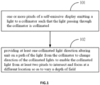
- FIG. 1 is a flow diagram of a near-eye displaying method capable of multiple depths of field imaging according to the present invention; the method comprises the steps of:
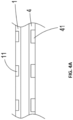
- a self-emissive display 1 utilized technology that enables self-emission; and the self-emissive display 1 may be a transparent display or a non-transparent display.
- the self-emissive display 1 may comprise active light sources such as organic light-emitting diodes (OLED), micro light emitting diodes (micro LED), quantum dot light emitters, or lasers... etc.
- the collimator may be a microlens, a liquid crystal spatial light modulator (LCSLM) or a flat metalens.
- LCDMSLM liquid crystal spatial light modulator
- the collimated light direction altering unit is a microlens, a liquid crystal spatial light modulator (LCSLM) or a flat metalens. According to the invention, the collimated light direction altering unit is a liquid crystal spatial light modulator.
- the collimated light direction altering unit is a liquid crystal spatial light modulator.
- the combinations are described as the following:
- the collimator is a microlens 2
- the collimated light direction altering unit is a liquid crystal spatial light modulator 3.
- one of the liquid crystal cells 31 of the liquid crystal spatial light modulator 3 adjusts the direction of light from one or more of the pixels 11, so that lights of two pixels 11 can extend and form a virtual image 51.
- the phase of one of the liquid crystal cells 31 can be changed to alter the direction of the collimated light such that lights of two pixels 11 can overlap at another location to form another virtual image 52 so as to extend the depth of field.
- the phase of the liquid crystal cells 31 can be adjusted constantly so that human eyes 6 are able to view multiple continuous virtual images to achieve multiple depths of field imaging.
- a single element can be utilized to collimate and change the direction of the light.
- the description is as the following:
Landscapes
- Physics & Mathematics (AREA)
- Engineering & Computer Science (AREA)
- Microelectronics & Electronic Packaging (AREA)
- General Physics & Mathematics (AREA)
- Optics & Photonics (AREA)
- Power Engineering (AREA)
- Computer Hardware Design (AREA)
- Condensed Matter Physics & Semiconductors (AREA)
- Nonlinear Science (AREA)
- Manufacturing & Machinery (AREA)
- Geometry (AREA)
- Liquid Crystal (AREA)
- Devices For Indicating Variable Information By Combining Individual Elements (AREA)
- Electroluminescent Light Sources (AREA)
Applications Claiming Priority (1)
| Application Number | Priority Date | Filing Date | Title |
|---|---|---|---|
| PCT/CN2018/077715 WO2019165620A1 (zh) | 2018-03-01 | 2018-03-01 | 具有多重景深显像的近眼显示方法 |
Publications (3)
| Publication Number | Publication Date |
|---|---|
| EP3761102A1 EP3761102A1 (en) | 2021-01-06 |
| EP3761102A4 EP3761102A4 (en) | 2021-10-27 |
| EP3761102B1 true EP3761102B1 (en) | 2023-11-29 |
Family
ID=67804822
Family Applications (2)
| Application Number | Title | Priority Date | Filing Date |
|---|---|---|---|
| EP18907507.0A Active EP3761102B1 (en) | 2018-03-01 | 2018-03-01 | Near eye display method capable of multi-depth of field imaging |
| EP19760179.2A Withdrawn EP3761364A4 (en) | 2018-03-01 | 2019-03-01 | DISPLAY COMPONENT AND DISPLAY DEVICE |
Family Applications After (1)
| Application Number | Title | Priority Date | Filing Date |
|---|---|---|---|
| EP19760179.2A Withdrawn EP3761364A4 (en) | 2018-03-01 | 2019-03-01 | DISPLAY COMPONENT AND DISPLAY DEVICE |
Country Status (7)
| Country | Link |
|---|---|
| US (2) | US11927871B2 (zh) |
| EP (2) | EP3761102B1 (zh) |
| JP (2) | JP7195653B2 (zh) |
| KR (2) | KR20200127023A (zh) |
| CN (2) | CN111837068A (zh) |
| TW (1) | TW201937234A (zh) |
| WO (2) | WO2019165620A1 (zh) |
Families Citing this family (9)
| Publication number | Priority date | Publication date | Assignee | Title |
|---|---|---|---|---|
| KR20200127023A (ko) | 2018-03-01 | 2020-11-09 | 에이치이에스 아이피 홀딩스, 엘엘씨 | 다중 피사계 심도 촬영이 가능한 근안 디스플레이 방법 |
| CN110910769B (zh) * | 2019-11-29 | 2022-04-08 | 京东方科技集团股份有限公司 | 虚拟显示装置及其制备方法、控制方法 |
| US11206978B2 (en) | 2020-04-01 | 2021-12-28 | Massachusetts Institute Of Technology | Meta-optics-based systems and methods for ocular applications |
| JP2023539962A (ja) | 2020-08-14 | 2023-09-21 | ヒーズ アイピー ホールディングス エルエルシー | リアルタイム画像上に仮想画像を重ね合わせるためのシステムおよび方法 |
| TWI838640B (zh) | 2020-09-03 | 2024-04-11 | 美商海思智財控股有限公司 | 改善雙眼視覺的系統與方法 |
| TWI838651B (zh) | 2020-09-30 | 2024-04-11 | 美商海思智財控股有限公司 | 用於虛擬實境及擴增實境裝置的虛擬影像顯示系統 |
| CN115280219A (zh) * | 2021-02-08 | 2022-11-01 | 海思智财控股有限公司 | 强化视力的系统与方法 |
| US20230201067A1 (en) * | 2021-06-11 | 2023-06-29 | Hes Ip Holdings, Llc | Systems and methods for improving vision of a viewer's eye with impaired retina |
| WO2024034502A1 (ja) * | 2022-08-09 | 2024-02-15 | ソニーセミコンダクタソリューションズ株式会社 | 発光装置および電子機器 |
Family Cites Families (44)
| Publication number | Priority date | Publication date | Assignee | Title |
|---|---|---|---|---|
| JP3136178B2 (ja) | 1991-10-09 | 2001-02-19 | 株式会社リコー | ディスプレイ装置 |
| JPH11234705A (ja) * | 1998-02-17 | 1999-08-27 | Matsushita Electric Ind Co Ltd | 立体表示装置 |
| JP2002090704A (ja) | 2000-09-18 | 2002-03-27 | Katsumi Yoshino | 液晶表示パネル読取装置 |
| JP4491948B2 (ja) * | 2000-10-06 | 2010-06-30 | ソニー株式会社 | 素子実装方法および画像表示装置の製造方法 |
| SG143942A1 (en) | 2001-02-19 | 2008-07-29 | Semiconductor Energy Lab | Light emitting device and method of manufacturing the same |
| JP2005175417A (ja) | 2003-07-28 | 2005-06-30 | Ricoh Co Ltd | 発光素子アレイ、光書込ユニットおよび画像形成装置 |
| JP2007027157A (ja) | 2005-07-12 | 2007-02-01 | Akita Denshi Systems:Kk | 発光ダイオード装置及びその製造方法並びに照明装置 |
| JP4839795B2 (ja) | 2005-11-24 | 2011-12-21 | ソニー株式会社 | 3次元表示装置 |
| US7782278B2 (en) * | 2006-12-14 | 2010-08-24 | Himax Technologies Limited | Intra-pixel convolution for AMOLED |
| JP2011145607A (ja) | 2010-01-18 | 2011-07-28 | Sony Corp | ヘッドマウントディスプレイ |
| US9436015B2 (en) | 2012-12-21 | 2016-09-06 | Reald Inc. | Superlens component for directional display |
| US20130285885A1 (en) | 2012-04-25 | 2013-10-31 | Andreas G. Nowatzyk | Head-mounted light-field display |
| CN102629667B (zh) | 2012-04-25 | 2015-03-25 | 上海大学 | 硅基顶发射有机发光微显示器及其制备方法 |
| US9841537B2 (en) * | 2012-07-02 | 2017-12-12 | Nvidia Corporation | Near-eye microlens array displays |
| US9860522B2 (en) | 2012-08-04 | 2018-01-02 | Paul Lapstun | Head-mounted light field display |
| US20140056003A1 (en) | 2012-08-20 | 2014-02-27 | John Frattalone | Modular video and lighting displays |
| US9442460B2 (en) | 2012-10-31 | 2016-09-13 | Lg Display Co., Ltd. | Digital hologram display device |
| JP6337433B2 (ja) | 2013-09-13 | 2018-06-06 | セイコーエプソン株式会社 | 頭部装着型表示装置および頭部装着型表示装置の制御方法 |
| KR102053440B1 (ko) * | 2013-09-26 | 2020-01-08 | 엘지디스플레이 주식회사 | 고 개구율 유기발광 다이오드 표시장치 및 그 제조 방법 |
| GB2525862A (en) | 2014-05-06 | 2015-11-11 | Univ Bedfordshire | Lens array and imaging device |
| JP6305855B2 (ja) | 2014-07-11 | 2018-04-04 | オリンパス株式会社 | 画像表示装置 |
| GB201413578D0 (en) | 2014-07-31 | 2014-09-17 | Infiniled Ltd | A colour iled display on silicon |
| GB201418772D0 (en) | 2014-10-22 | 2014-12-03 | Infiniled Ltd | Display |
| KR102312576B1 (ko) * | 2014-11-05 | 2021-10-14 | 엘지디스플레이 주식회사 | 유기전계발광표시장치 및 그 제조방법 |
| CN105739094A (zh) | 2014-12-11 | 2016-07-06 | 北京邮电大学 | 一种基于透镜阵列的近眼显示方法 |
| WO2016163231A1 (ja) | 2015-04-09 | 2016-10-13 | シャープ株式会社 | 眼鏡型表示装置 |
| US9939129B2 (en) * | 2015-09-23 | 2018-04-10 | Osram Sylvania Inc. | Collimating metalenses and technologies incorporating the same |
| FR3044467B1 (fr) | 2015-11-26 | 2018-08-10 | Commissariat A L'energie Atomique Et Aux Energies Alternatives | Dalle lumineuse et procede de fabrication d'une telle dalle lumineuse |
| CN105449125B (zh) | 2015-12-03 | 2018-11-09 | 东南大学 | 一种硅基量子点显示器及其制作方法 |
| TWI696847B (zh) | 2016-01-28 | 2020-06-21 | 中強光電股份有限公司 | 頭戴式顯示裝置 |
| US9964767B2 (en) | 2016-03-03 | 2018-05-08 | Google Llc | Display with reflected LED micro-display panels |
| WO2018013307A1 (en) | 2016-06-21 | 2018-01-18 | Ntt Docomo, Inc. | An illuminator for a wearable display |
| CN107561702A (zh) | 2016-07-01 | 2018-01-09 | 成都理想境界科技有限公司 | 一种近眼显示系统、虚拟现实设备和增强现实设备 |
| CN107561697B (zh) | 2016-07-01 | 2019-04-30 | 成都理想境界科技有限公司 | 近眼显示系统、虚拟现实设备及增强现实设备 |
| CN105911791A (zh) | 2016-07-04 | 2016-08-31 | 京东方科技集团股份有限公司 | 一种显示面板及显示装置 |
| CN107664840A (zh) | 2016-07-28 | 2018-02-06 | 中强光电股份有限公司 | 头戴式显示装置 |
| CN106057843B (zh) | 2016-08-05 | 2019-04-30 | 京东方科技集团股份有限公司 | 透明显示面板、透明显示装置及透明显示面板的制作方法 |
| TWI607243B (zh) | 2016-08-09 | 2017-12-01 | Tai Guo Chen | Display adjustment method for near-eye display |
| CN106292240A (zh) | 2016-09-05 | 2017-01-04 | 京东方科技集团股份有限公司 | 全息显示装置及其显示方法 |
| CN106526864B (zh) * | 2017-01-05 | 2019-08-30 | 京东方科技集团股份有限公司 | 显示装置和显示方法 |
| CN106873161B (zh) | 2017-03-02 | 2020-03-17 | 上海天马微电子有限公司 | 一种显示装置及近眼可穿戴设备 |
| CN107490862B (zh) | 2017-03-23 | 2019-10-25 | 华为机器有限公司 | 近眼显示器及近眼显示系统 |
| CN106932916B (zh) | 2017-05-04 | 2019-10-01 | 鲁东大学 | 一种利用超材料透镜的双光束超分辨聚焦方法 |
| KR20200127023A (ko) | 2018-03-01 | 2020-11-09 | 에이치이에스 아이피 홀딩스, 엘엘씨 | 다중 피사계 심도 촬영이 가능한 근안 디스플레이 방법 |
-
2018
- 2018-03-01 KR KR1020207028341A patent/KR20200127023A/ko not_active Application Discontinuation
- 2018-03-01 EP EP18907507.0A patent/EP3761102B1/en active Active
- 2018-03-01 CN CN201880090627.7A patent/CN111837068A/zh active Pending
- 2018-03-01 JP JP2020568582A patent/JP7195653B2/ja active Active
- 2018-03-01 WO PCT/CN2018/077715 patent/WO2019165620A1/zh unknown
- 2018-03-01 US US16/976,506 patent/US11927871B2/en active Active
-
2019
- 2019-02-28 TW TW108106943A patent/TW201937234A/zh unknown
- 2019-03-01 US US16/976,526 patent/US20210005681A1/en not_active Abandoned
- 2019-03-01 JP JP2020568586A patent/JP2021520523A/ja active Pending
- 2019-03-01 EP EP19760179.2A patent/EP3761364A4/en not_active Withdrawn
- 2019-03-01 KR KR1020207028337A patent/KR20200127235A/ko not_active Application Discontinuation
- 2019-03-01 WO PCT/CN2019/076752 patent/WO2019166018A1/zh unknown
- 2019-03-01 CN CN201980016537.8A patent/CN111801803A/zh active Pending
Also Published As
| Publication number | Publication date |
|---|---|
| TW201937234A (zh) | 2019-09-16 |
| EP3761102A4 (en) | 2021-10-27 |
| US11927871B2 (en) | 2024-03-12 |
| EP3761364A1 (en) | 2021-01-06 |
| US20210005681A1 (en) | 2021-01-07 |
| WO2019166018A1 (zh) | 2019-09-06 |
| JP2021521494A (ja) | 2021-08-26 |
| KR20200127023A (ko) | 2020-11-09 |
| CN111837068A (zh) | 2020-10-27 |
| US20210003900A1 (en) | 2021-01-07 |
| CN111801803A (zh) | 2020-10-20 |
| EP3761102A1 (en) | 2021-01-06 |
| JP2021520523A (ja) | 2021-08-19 |
| JP7195653B2 (ja) | 2022-12-26 |
| WO2019165620A1 (zh) | 2019-09-06 |
| EP3761364A4 (en) | 2021-04-21 |
| KR20200127235A (ko) | 2020-11-10 |
Similar Documents
| Publication | Publication Date | Title |
|---|---|---|
| EP3761102B1 (en) | Near eye display method capable of multi-depth of field imaging | |
| US11303880B2 (en) | Near eye wavefront emulating display | |
| US11256095B2 (en) | Reflective switching device for inputting different wavelengths of light into waveguides | |
| US9684174B2 (en) | Imaging structure with embedded light sources | |
| CN110651216B (zh) | 低轮廓分束器 | |
| US9726887B2 (en) | Imaging structure color conversion | |
| JP7391842B2 (ja) | 表示装置および表示システム | |
| US10659770B2 (en) | Stereo image display apparatus | |
| KR20140018209A (ko) | 픽셀 렌즈를 갖춘 콜리메이팅 디스플레이 | |
| JP2011501822A (ja) | 表示装置及びその表示方法 | |
| US11454815B2 (en) | Transparent optical module using pixel patches and associated lenslets | |
| US10613376B2 (en) | Augmented reality see-through display | |
| TWI691739B (zh) | 具有多重景深顯像的近眼顯示方法 | |
| EP3918781B1 (en) | Display system having 1-dimensional pixel array with scanning mirror | |
| CN108965857A (zh) | 一种立体显示方法及装置、可穿戴式立体显示器 |
Legal Events
| Date | Code | Title | Description |
|---|---|---|---|
| STAA | Information on the status of an ep patent application or granted ep patent |
Free format text: STATUS: THE INTERNATIONAL PUBLICATION HAS BEEN MADE |
|
| PUAI | Public reference made under article 153(3) epc to a published international application that has entered the european phase |
Free format text: ORIGINAL CODE: 0009012 |
|
| STAA | Information on the status of an ep patent application or granted ep patent |
Free format text: STATUS: REQUEST FOR EXAMINATION WAS MADE |
|
| 17P | Request for examination filed |
Effective date: 20200925 |
|
| AK | Designated contracting states |
Kind code of ref document: A1 Designated state(s): AL AT BE BG CH CY CZ DE DK EE ES FI FR GB GR HR HU IE IS IT LI LT LU LV MC MK MT NL NO PL PT RO RS SE SI SK SM TR |
|
| AX | Request for extension of the european patent |
Extension state: BA ME |
|
| DAV | Request for validation of the european patent (deleted) | ||
| DAX | Request for extension of the european patent (deleted) | ||
| A4 | Supplementary search report drawn up and despatched |
Effective date: 20210924 |
|
| RIC1 | Information provided on ipc code assigned before grant |
Ipc: H01L 25/075 20060101ALN20210920BHEP Ipc: H01L 25/16 20060101ALN20210920BHEP Ipc: H01L 33/58 20100101ALI20210920BHEP Ipc: H01L 27/32 20060101ALI20210920BHEP Ipc: G02B 3/00 20060101ALI20210920BHEP Ipc: G02B 27/01 20060101AFI20210920BHEP |
|
| STAA | Information on the status of an ep patent application or granted ep patent |
Free format text: STATUS: EXAMINATION IS IN PROGRESS |
|
| 17Q | First examination report despatched |
Effective date: 20221107 |
|
| GRAP | Despatch of communication of intention to grant a patent |
Free format text: ORIGINAL CODE: EPIDOSNIGR1 |
|
| STAA | Information on the status of an ep patent application or granted ep patent |
Free format text: STATUS: GRANT OF PATENT IS INTENDED |
|
| RIC1 | Information provided on ipc code assigned before grant |
Ipc: H01L 25/075 20060101ALN20230531BHEP Ipc: H01L 25/16 20060101ALN20230531BHEP Ipc: H01L 33/58 20100101ALI20230531BHEP Ipc: H10K 59/35 20230101ALI20230531BHEP Ipc: G02B 3/00 20060101ALI20230531BHEP Ipc: G02B 27/01 20060101AFI20230531BHEP |
|
| P01 | Opt-out of the competence of the unified patent court (upc) registered |
Effective date: 20230526 |
|
| RIC1 | Information provided on ipc code assigned before grant |
Ipc: H01L 25/075 20060101ALN20230609BHEP Ipc: H01L 25/16 20060101ALN20230609BHEP Ipc: H01L 33/58 20100101ALI20230609BHEP Ipc: H10K 59/35 20230101ALI20230609BHEP Ipc: G02B 3/00 20060101ALI20230609BHEP Ipc: G02B 27/01 20060101AFI20230609BHEP |
|
| INTG | Intention to grant announced |
Effective date: 20230630 |
|
| GRAS | Grant fee paid |
Free format text: ORIGINAL CODE: EPIDOSNIGR3 |
|
| GRAA | (expected) grant |
Free format text: ORIGINAL CODE: 0009210 |
|
| STAA | Information on the status of an ep patent application or granted ep patent |
Free format text: STATUS: THE PATENT HAS BEEN GRANTED |
|
| AK | Designated contracting states |
Kind code of ref document: B1 Designated state(s): AL AT BE BG CH CY CZ DE DK EE ES FI FR GB GR HR HU IE IS IT LI LT LU LV MC MK MT NL NO PL PT RO RS SE SI SK SM TR |
|
| REG | Reference to a national code |
Ref country code: GB Ref legal event code: FG4D |
|
| REG | Reference to a national code |
Ref country code: CH Ref legal event code: EP |
|
| REG | Reference to a national code |
Ref country code: IE Ref legal event code: FG4D |
|
| REG | Reference to a national code |
Ref country code: DE Ref legal event code: R096 Ref document number: 602018062037 Country of ref document: DE |
|
| REG | Reference to a national code |
Ref country code: NL Ref legal event code: FP |
|
| REG | Reference to a national code |
Ref country code: LT Ref legal event code: MG9D |
|
| PG25 | Lapsed in a contracting state [announced via postgrant information from national office to epo] |
Ref country code: GR Free format text: LAPSE BECAUSE OF FAILURE TO SUBMIT A TRANSLATION OF THE DESCRIPTION OR TO PAY THE FEE WITHIN THE PRESCRIBED TIME-LIMIT Effective date: 20240301 |
|
| PG25 | Lapsed in a contracting state [announced via postgrant information from national office to epo] |
Ref country code: IS Free format text: LAPSE BECAUSE OF FAILURE TO SUBMIT A TRANSLATION OF THE DESCRIPTION OR TO PAY THE FEE WITHIN THE PRESCRIBED TIME-LIMIT Effective date: 20240329 |
|
| PG25 | Lapsed in a contracting state [announced via postgrant information from national office to epo] |
Ref country code: LT Free format text: LAPSE BECAUSE OF FAILURE TO SUBMIT A TRANSLATION OF THE DESCRIPTION OR TO PAY THE FEE WITHIN THE PRESCRIBED TIME-LIMIT Effective date: 20231129 |
|
| PGFP | Annual fee paid to national office [announced via postgrant information from national office to epo] |
Ref country code: NL Payment date: 20240320 Year of fee payment: 7 |
|
| PG25 | Lapsed in a contracting state [announced via postgrant information from national office to epo] |
Ref country code: ES Free format text: LAPSE BECAUSE OF FAILURE TO SUBMIT A TRANSLATION OF THE DESCRIPTION OR TO PAY THE FEE WITHIN THE PRESCRIBED TIME-LIMIT Effective date: 20231129 |
|
| PG25 | Lapsed in a contracting state [announced via postgrant information from national office to epo] |
Ref country code: LT Free format text: LAPSE BECAUSE OF FAILURE TO SUBMIT A TRANSLATION OF THE DESCRIPTION OR TO PAY THE FEE WITHIN THE PRESCRIBED TIME-LIMIT Effective date: 20231129 Ref country code: IS Free format text: LAPSE BECAUSE OF FAILURE TO SUBMIT A TRANSLATION OF THE DESCRIPTION OR TO PAY THE FEE WITHIN THE PRESCRIBED TIME-LIMIT Effective date: 20240329 Ref country code: GR Free format text: LAPSE BECAUSE OF FAILURE TO SUBMIT A TRANSLATION OF THE DESCRIPTION OR TO PAY THE FEE WITHIN THE PRESCRIBED TIME-LIMIT Effective date: 20240301 Ref country code: ES Free format text: LAPSE BECAUSE OF FAILURE TO SUBMIT A TRANSLATION OF THE DESCRIPTION OR TO PAY THE FEE WITHIN THE PRESCRIBED TIME-LIMIT Effective date: 20231129 Ref country code: BG Free format text: LAPSE BECAUSE OF FAILURE TO SUBMIT A TRANSLATION OF THE DESCRIPTION OR TO PAY THE FEE WITHIN THE PRESCRIBED TIME-LIMIT Effective date: 20240229 |
|
| PGFP | Annual fee paid to national office [announced via postgrant information from national office to epo] |
Ref country code: DE Payment date: 20240327 Year of fee payment: 7 Ref country code: GB Payment date: 20240321 Year of fee payment: 7 |
|
| REG | Reference to a national code |
Ref country code: AT Ref legal event code: MK05 Ref document number: 1636730 Country of ref document: AT Kind code of ref document: T Effective date: 20231129 |
|
| PG25 | Lapsed in a contracting state [announced via postgrant information from national office to epo] |
Ref country code: SE Free format text: LAPSE BECAUSE OF FAILURE TO SUBMIT A TRANSLATION OF THE DESCRIPTION OR TO PAY THE FEE WITHIN THE PRESCRIBED TIME-LIMIT Effective date: 20231129 Ref country code: RS Free format text: LAPSE BECAUSE OF FAILURE TO SUBMIT A TRANSLATION OF THE DESCRIPTION OR TO PAY THE FEE WITHIN THE PRESCRIBED TIME-LIMIT Effective date: 20231129 Ref country code: PL Free format text: LAPSE BECAUSE OF FAILURE TO SUBMIT A TRANSLATION OF THE DESCRIPTION OR TO PAY THE FEE WITHIN THE PRESCRIBED TIME-LIMIT Effective date: 20231129 Ref country code: NO Free format text: LAPSE BECAUSE OF FAILURE TO SUBMIT A TRANSLATION OF THE DESCRIPTION OR TO PAY THE FEE WITHIN THE PRESCRIBED TIME-LIMIT Effective date: 20240229 Ref country code: LV Free format text: LAPSE BECAUSE OF FAILURE TO SUBMIT A TRANSLATION OF THE DESCRIPTION OR TO PAY THE FEE WITHIN THE PRESCRIBED TIME-LIMIT Effective date: 20231129 Ref country code: HR Free format text: LAPSE BECAUSE OF FAILURE TO SUBMIT A TRANSLATION OF THE DESCRIPTION OR TO PAY THE FEE WITHIN THE PRESCRIBED TIME-LIMIT Effective date: 20231129 |
|
| PGFP | Annual fee paid to national office [announced via postgrant information from national office to epo] |
Ref country code: FR Payment date: 20240328 Year of fee payment: 7 |
|
| PG25 | Lapsed in a contracting state [announced via postgrant information from national office to epo] |
Ref country code: DK Free format text: LAPSE BECAUSE OF FAILURE TO SUBMIT A TRANSLATION OF THE DESCRIPTION OR TO PAY THE FEE WITHIN THE PRESCRIBED TIME-LIMIT Effective date: 20231129 |
|
| PG25 | Lapsed in a contracting state [announced via postgrant information from national office to epo] |
Ref country code: AT Free format text: LAPSE BECAUSE OF FAILURE TO SUBMIT A TRANSLATION OF THE DESCRIPTION OR TO PAY THE FEE WITHIN THE PRESCRIBED TIME-LIMIT Effective date: 20231129 Ref country code: CZ Free format text: LAPSE BECAUSE OF FAILURE TO SUBMIT A TRANSLATION OF THE DESCRIPTION OR TO PAY THE FEE WITHIN THE PRESCRIBED TIME-LIMIT Effective date: 20231129 |
|
| PG25 | Lapsed in a contracting state [announced via postgrant information from national office to epo] |
Ref country code: SK Free format text: LAPSE BECAUSE OF FAILURE TO SUBMIT A TRANSLATION OF THE DESCRIPTION OR TO PAY THE FEE WITHIN THE PRESCRIBED TIME-LIMIT Effective date: 20231129 |
|
| PG25 | Lapsed in a contracting state [announced via postgrant information from national office to epo] |
Ref country code: SM Free format text: LAPSE BECAUSE OF FAILURE TO SUBMIT A TRANSLATION OF THE DESCRIPTION OR TO PAY THE FEE WITHIN THE PRESCRIBED TIME-LIMIT Effective date: 20231129 Ref country code: SK Free format text: LAPSE BECAUSE OF FAILURE TO SUBMIT A TRANSLATION OF THE DESCRIPTION OR TO PAY THE FEE WITHIN THE PRESCRIBED TIME-LIMIT Effective date: 20231129 Ref country code: RO Free format text: LAPSE BECAUSE OF FAILURE TO SUBMIT A TRANSLATION OF THE DESCRIPTION OR TO PAY THE FEE WITHIN THE PRESCRIBED TIME-LIMIT Effective date: 20231129 Ref country code: IT Free format text: LAPSE BECAUSE OF FAILURE TO SUBMIT A TRANSLATION OF THE DESCRIPTION OR TO PAY THE FEE WITHIN THE PRESCRIBED TIME-LIMIT Effective date: 20231129 Ref country code: EE Free format text: LAPSE BECAUSE OF FAILURE TO SUBMIT A TRANSLATION OF THE DESCRIPTION OR TO PAY THE FEE WITHIN THE PRESCRIBED TIME-LIMIT Effective date: 20231129 Ref country code: DK Free format text: LAPSE BECAUSE OF FAILURE TO SUBMIT A TRANSLATION OF THE DESCRIPTION OR TO PAY THE FEE WITHIN THE PRESCRIBED TIME-LIMIT Effective date: 20231129 Ref country code: CZ Free format text: LAPSE BECAUSE OF FAILURE TO SUBMIT A TRANSLATION OF THE DESCRIPTION OR TO PAY THE FEE WITHIN THE PRESCRIBED TIME-LIMIT Effective date: 20231129 Ref country code: AT Free format text: LAPSE BECAUSE OF FAILURE TO SUBMIT A TRANSLATION OF THE DESCRIPTION OR TO PAY THE FEE WITHIN THE PRESCRIBED TIME-LIMIT Effective date: 20231129 |
|
| PG25 | Lapsed in a contracting state [announced via postgrant information from national office to epo] |
Ref country code: PT Free format text: LAPSE BECAUSE OF FAILURE TO SUBMIT A TRANSLATION OF THE DESCRIPTION OR TO PAY THE FEE WITHIN THE PRESCRIBED TIME-LIMIT Effective date: 20240401 |
|
| PG25 | Lapsed in a contracting state [announced via postgrant information from national office to epo] |
Ref country code: PT Free format text: LAPSE BECAUSE OF FAILURE TO SUBMIT A TRANSLATION OF THE DESCRIPTION OR TO PAY THE FEE WITHIN THE PRESCRIBED TIME-LIMIT Effective date: 20240401 |
|
| REG | Reference to a national code |
Ref country code: DE Ref legal event code: R097 Ref document number: 602018062037 Country of ref document: DE |
|
| PLBE | No opposition filed within time limit |
Free format text: ORIGINAL CODE: 0009261 |
|
| STAA | Information on the status of an ep patent application or granted ep patent |
Free format text: STATUS: NO OPPOSITION FILED WITHIN TIME LIMIT |