EP3758072A1 - Solar cell design optimized for performance at high radiation doses - Google Patents
Solar cell design optimized for performance at high radiation doses Download PDFInfo
- Publication number
- EP3758072A1 EP3758072A1 EP20168452.9A EP20168452A EP3758072A1 EP 3758072 A1 EP3758072 A1 EP 3758072A1 EP 20168452 A EP20168452 A EP 20168452A EP 3758072 A1 EP3758072 A1 EP 3758072A1
- Authority
- EP
- European Patent Office
- Prior art keywords
- cell
- sub
- solar cell
- base
- reflector
- Prior art date
- Legal status (The legal status is an assumption and is not a legal conclusion. Google has not performed a legal analysis and makes no representation as to the accuracy of the status listed.)
- Pending
Links
- 230000005855 radiation Effects 0.000 title claims abstract description 54
- 238000013461 design Methods 0.000 title description 8
- 206010011906 Death Diseases 0.000 claims description 20
- 229910000530 Gallium indium arsenide Inorganic materials 0.000 claims description 18
- 230000014759 maintenance of location Effects 0.000 claims description 14
- 238000000034 method Methods 0.000 claims description 13
- FTWRSWRBSVXQPI-UHFFFAOYSA-N alumanylidynearsane;gallanylidynearsane Chemical compound [As]#[Al].[As]#[Ga] FTWRSWRBSVXQPI-UHFFFAOYSA-N 0.000 claims description 8
- JBRZTFJDHDCESZ-UHFFFAOYSA-N AsGa Chemical compound [As]#[Ga] JBRZTFJDHDCESZ-UHFFFAOYSA-N 0.000 claims description 7
- KXNLCSXBJCPWGL-UHFFFAOYSA-N [Ga].[As].[In] Chemical compound [Ga].[As].[In] KXNLCSXBJCPWGL-UHFFFAOYSA-N 0.000 claims description 7
- 238000004519 manufacturing process Methods 0.000 description 6
- 239000000463 material Substances 0.000 description 5
- 229910001218 Gallium arsenide Inorganic materials 0.000 description 4
- 230000008901 benefit Effects 0.000 description 4
- 229910052751 metal Inorganic materials 0.000 description 4
- 239000002184 metal Substances 0.000 description 4
- 238000010586 diagram Methods 0.000 description 3
- 230000004048 modification Effects 0.000 description 3
- 238000012986 modification Methods 0.000 description 3
- 238000010521 absorption reaction Methods 0.000 description 2
- GNPVGFCGXDBREM-UHFFFAOYSA-N germanium atom Chemical compound [Ge] GNPVGFCGXDBREM-UHFFFAOYSA-N 0.000 description 2
- 230000009467 reduction Effects 0.000 description 2
- 239000000758 substrate Substances 0.000 description 2
- VYPSYNLAJGMNEJ-UHFFFAOYSA-N Silicium dioxide Chemical compound O=[Si]=O VYPSYNLAJGMNEJ-UHFFFAOYSA-N 0.000 description 1
- 229910003087 TiOx Inorganic materials 0.000 description 1
- 229910052782 aluminium Inorganic materials 0.000 description 1
- PNEYBMLMFCGWSK-UHFFFAOYSA-N aluminium oxide Inorganic materials [O-2].[O-2].[O-2].[Al+3].[Al+3] PNEYBMLMFCGWSK-UHFFFAOYSA-N 0.000 description 1
- AJGDITRVXRPLBY-UHFFFAOYSA-N aluminum indium Chemical compound [Al].[In] AJGDITRVXRPLBY-UHFFFAOYSA-N 0.000 description 1
- 239000000969 carrier Substances 0.000 description 1
- 239000011248 coating agent Substances 0.000 description 1
- 238000000576 coating method Methods 0.000 description 1
- 230000001010 compromised effect Effects 0.000 description 1
- 229910052593 corundum Inorganic materials 0.000 description 1
- 238000009792 diffusion process Methods 0.000 description 1
- 238000000407 epitaxy Methods 0.000 description 1
- 229910052732 germanium Inorganic materials 0.000 description 1
- 229910052737 gold Inorganic materials 0.000 description 1
- 230000006872 improvement Effects 0.000 description 1
- 230000010354 integration Effects 0.000 description 1
- 238000012423 maintenance Methods 0.000 description 1
- 150000002739 metals Chemical class 0.000 description 1
- 229910052759 nickel Inorganic materials 0.000 description 1
- 230000006911 nucleation Effects 0.000 description 1
- 238000010899 nucleation Methods 0.000 description 1
- 230000008520 organization Effects 0.000 description 1
- 229910052697 platinum Inorganic materials 0.000 description 1
- 230000008569 process Effects 0.000 description 1
- 238000009419 refurbishment Methods 0.000 description 1
- 230000004044 response Effects 0.000 description 1
- 239000004065 semiconductor Substances 0.000 description 1
- 238000005389 semiconductor device fabrication Methods 0.000 description 1
- 229910052814 silicon oxide Inorganic materials 0.000 description 1
- 229910052709 silver Inorganic materials 0.000 description 1
- HLLICFJUWSZHRJ-UHFFFAOYSA-N tioxidazole Chemical compound CCCOC1=CC=C2N=C(NC(=O)OC)SC2=C1 HLLICFJUWSZHRJ-UHFFFAOYSA-N 0.000 description 1
- 229910052719 titanium Inorganic materials 0.000 description 1
- 229910001845 yogo sapphire Inorganic materials 0.000 description 1
Images



Classifications
-
- H—ELECTRICITY
- H10—SEMICONDUCTOR DEVICES; ELECTRIC SOLID-STATE DEVICES NOT OTHERWISE PROVIDED FOR
- H10F—INORGANIC SEMICONDUCTOR DEVICES SENSITIVE TO INFRARED RADIATION, LIGHT, ELECTROMAGNETIC RADIATION OF SHORTER WAVELENGTH OR CORPUSCULAR RADIATION
- H10F77/00—Constructional details of devices covered by this subclass
- H10F77/10—Semiconductor bodies
- H10F77/14—Shape of semiconductor bodies; Shapes, relative sizes or dispositions of semiconductor regions within semiconductor bodies
-
- H—ELECTRICITY
- H10—SEMICONDUCTOR DEVICES; ELECTRIC SOLID-STATE DEVICES NOT OTHERWISE PROVIDED FOR
- H10F—INORGANIC SEMICONDUCTOR DEVICES SENSITIVE TO INFRARED RADIATION, LIGHT, ELECTROMAGNETIC RADIATION OF SHORTER WAVELENGTH OR CORPUSCULAR RADIATION
- H10F77/00—Constructional details of devices covered by this subclass
- H10F77/80—Arrangements for preventing damage to photovoltaic cells caused by corpuscular radiation, e.g. for space applications
-
- H—ELECTRICITY
- H10—SEMICONDUCTOR DEVICES; ELECTRIC SOLID-STATE DEVICES NOT OTHERWISE PROVIDED FOR
- H10F—INORGANIC SEMICONDUCTOR DEVICES SENSITIVE TO INFRARED RADIATION, LIGHT, ELECTROMAGNETIC RADIATION OF SHORTER WAVELENGTH OR CORPUSCULAR RADIATION
- H10F10/00—Individual photovoltaic cells, e.g. solar cells
- H10F10/10—Individual photovoltaic cells, e.g. solar cells having potential barriers
- H10F10/14—Photovoltaic cells having only PN homojunction potential barriers
- H10F10/142—Photovoltaic cells having only PN homojunction potential barriers comprising multiple PN homojunctions, e.g. tandem cells
-
- H—ELECTRICITY
- H10—SEMICONDUCTOR DEVICES; ELECTRIC SOLID-STATE DEVICES NOT OTHERWISE PROVIDED FOR
- H10F—INORGANIC SEMICONDUCTOR DEVICES SENSITIVE TO INFRARED RADIATION, LIGHT, ELECTROMAGNETIC RADIATION OF SHORTER WAVELENGTH OR CORPUSCULAR RADIATION
- H10F10/00—Individual photovoltaic cells, e.g. solar cells
- H10F10/10—Individual photovoltaic cells, e.g. solar cells having potential barriers
- H10F10/14—Photovoltaic cells having only PN homojunction potential barriers
- H10F10/144—Photovoltaic cells having only PN homojunction potential barriers comprising only Group III-V materials, e.g. GaAs,AlGaAs, or InP photovoltaic cells
-
- H—ELECTRICITY
- H10—SEMICONDUCTOR DEVICES; ELECTRIC SOLID-STATE DEVICES NOT OTHERWISE PROVIDED FOR
- H10F—INORGANIC SEMICONDUCTOR DEVICES SENSITIVE TO INFRARED RADIATION, LIGHT, ELECTROMAGNETIC RADIATION OF SHORTER WAVELENGTH OR CORPUSCULAR RADIATION
- H10F10/00—Individual photovoltaic cells, e.g. solar cells
- H10F10/10—Individual photovoltaic cells, e.g. solar cells having potential barriers
- H10F10/16—Photovoltaic cells having only PN heterojunction potential barriers
- H10F10/163—Photovoltaic cells having only PN heterojunction potential barriers comprising only Group III-V materials, e.g. GaAs/AlGaAs or InP/GaInAs photovoltaic cells
-
- H—ELECTRICITY
- H10—SEMICONDUCTOR DEVICES; ELECTRIC SOLID-STATE DEVICES NOT OTHERWISE PROVIDED FOR
- H10F—INORGANIC SEMICONDUCTOR DEVICES SENSITIVE TO INFRARED RADIATION, LIGHT, ELECTROMAGNETIC RADIATION OF SHORTER WAVELENGTH OR CORPUSCULAR RADIATION
- H10F71/00—Manufacture or treatment of devices covered by this subclass
- H10F71/127—The active layers comprising only Group III-V materials, e.g. GaAs or InP
-
- H—ELECTRICITY
- H10—SEMICONDUCTOR DEVICES; ELECTRIC SOLID-STATE DEVICES NOT OTHERWISE PROVIDED FOR
- H10F—INORGANIC SEMICONDUCTOR DEVICES SENSITIVE TO INFRARED RADIATION, LIGHT, ELECTROMAGNETIC RADIATION OF SHORTER WAVELENGTH OR CORPUSCULAR RADIATION
- H10F71/00—Manufacture or treatment of devices covered by this subclass
- H10F71/127—The active layers comprising only Group III-V materials, e.g. GaAs or InP
- H10F71/1272—The active layers comprising only Group III-V materials, e.g. GaAs or InP comprising at least three elements, e.g. GaAlAs or InGaAsP
-
- H—ELECTRICITY
- H10—SEMICONDUCTOR DEVICES; ELECTRIC SOLID-STATE DEVICES NOT OTHERWISE PROVIDED FOR
- H10F—INORGANIC SEMICONDUCTOR DEVICES SENSITIVE TO INFRARED RADIATION, LIGHT, ELECTROMAGNETIC RADIATION OF SHORTER WAVELENGTH OR CORPUSCULAR RADIATION
- H10F77/00—Constructional details of devices covered by this subclass
- H10F77/10—Semiconductor bodies
- H10F77/12—Active materials
- H10F77/124—Active materials comprising only Group III-V materials, e.g. GaAs
- H10F77/1248—Active materials comprising only Group III-V materials, e.g. GaAs having three or more elements, e.g. GaAlAs, InGaAs or InGaAsP
-
- H—ELECTRICITY
- H10—SEMICONDUCTOR DEVICES; ELECTRIC SOLID-STATE DEVICES NOT OTHERWISE PROVIDED FOR
- H10F—INORGANIC SEMICONDUCTOR DEVICES SENSITIVE TO INFRARED RADIATION, LIGHT, ELECTROMAGNETIC RADIATION OF SHORTER WAVELENGTH OR CORPUSCULAR RADIATION
- H10F77/00—Constructional details of devices covered by this subclass
- H10F77/40—Optical elements or arrangements
- H10F77/42—Optical elements or arrangements directly associated or integrated with photovoltaic cells, e.g. light-reflecting means or light-concentrating means
-
- H—ELECTRICITY
- H10—SEMICONDUCTOR DEVICES; ELECTRIC SOLID-STATE DEVICES NOT OTHERWISE PROVIDED FOR
- H10F—INORGANIC SEMICONDUCTOR DEVICES SENSITIVE TO INFRARED RADIATION, LIGHT, ELECTROMAGNETIC RADIATION OF SHORTER WAVELENGTH OR CORPUSCULAR RADIATION
- H10F77/00—Constructional details of devices covered by this subclass
- H10F77/40—Optical elements or arrangements
- H10F77/42—Optical elements or arrangements directly associated or integrated with photovoltaic cells, e.g. light-reflecting means or light-concentrating means
- H10F77/48—Back surface reflectors [BSR]
-
- H—ELECTRICITY
- H10—SEMICONDUCTOR DEVICES; ELECTRIC SOLID-STATE DEVICES NOT OTHERWISE PROVIDED FOR
- H10F—INORGANIC SEMICONDUCTOR DEVICES SENSITIVE TO INFRARED RADIATION, LIGHT, ELECTROMAGNETIC RADIATION OF SHORTER WAVELENGTH OR CORPUSCULAR RADIATION
- H10F77/00—Constructional details of devices covered by this subclass
- H10F77/40—Optical elements or arrangements
- H10F77/42—Optical elements or arrangements directly associated or integrated with photovoltaic cells, e.g. light-reflecting means or light-concentrating means
- H10F77/492—Spectrum-splitting means, e.g. dichroic mirrors
-
- Y—GENERAL TAGGING OF NEW TECHNOLOGICAL DEVELOPMENTS; GENERAL TAGGING OF CROSS-SECTIONAL TECHNOLOGIES SPANNING OVER SEVERAL SECTIONS OF THE IPC; TECHNICAL SUBJECTS COVERED BY FORMER USPC CROSS-REFERENCE ART COLLECTIONS [XRACs] AND DIGESTS
- Y02—TECHNOLOGIES OR APPLICATIONS FOR MITIGATION OR ADAPTATION AGAINST CLIMATE CHANGE
- Y02E—REDUCTION OF GREENHOUSE GAS [GHG] EMISSIONS, RELATED TO ENERGY GENERATION, TRANSMISSION OR DISTRIBUTION
- Y02E10/00—Energy generation through renewable energy sources
- Y02E10/50—Photovoltaic [PV] energy
- Y02E10/52—PV systems with concentrators
-
- Y—GENERAL TAGGING OF NEW TECHNOLOGICAL DEVELOPMENTS; GENERAL TAGGING OF CROSS-SECTIONAL TECHNOLOGIES SPANNING OVER SEVERAL SECTIONS OF THE IPC; TECHNICAL SUBJECTS COVERED BY FORMER USPC CROSS-REFERENCE ART COLLECTIONS [XRACs] AND DIGESTS
- Y02—TECHNOLOGIES OR APPLICATIONS FOR MITIGATION OR ADAPTATION AGAINST CLIMATE CHANGE
- Y02E—REDUCTION OF GREENHOUSE GAS [GHG] EMISSIONS, RELATED TO ENERGY GENERATION, TRANSMISSION OR DISTRIBUTION
- Y02E10/00—Energy generation through renewable energy sources
- Y02E10/50—Photovoltaic [PV] energy
- Y02E10/544—Solar cells from Group III-V materials
-
- Y—GENERAL TAGGING OF NEW TECHNOLOGICAL DEVELOPMENTS; GENERAL TAGGING OF CROSS-SECTIONAL TECHNOLOGIES SPANNING OVER SEVERAL SECTIONS OF THE IPC; TECHNICAL SUBJECTS COVERED BY FORMER USPC CROSS-REFERENCE ART COLLECTIONS [XRACs] AND DIGESTS
- Y02—TECHNOLOGIES OR APPLICATIONS FOR MITIGATION OR ADAPTATION AGAINST CLIMATE CHANGE
- Y02P—CLIMATE CHANGE MITIGATION TECHNOLOGIES IN THE PRODUCTION OR PROCESSING OF GOODS
- Y02P70/00—Climate change mitigation technologies in the production process for final industrial or consumer products
- Y02P70/50—Manufacturing or production processes characterised by the final manufactured product
Definitions
- the '313 patent specifies the use of a semiconductor mirror disposed between two partial cells, with the thickness of the partial cell above the mirror cut in half by using the mirror, without drastically reducing the absorption of the partial cell.
- the design of the ' 313 patent falls off in performance quickly after high radiation doses of about 1e15 e-/cm 2 or greater.
- the present disclosure describes a device, a method of fabricating the device, and a method of generating a current using the device, wherein the device is a solar cell optimized for performance at high radiation doses, and the solar cell includes: a sub-cell comprised of a base and an emitter; the base of the sub-cell has a thickness of about 2 to 3 ⁇ m; the base of the sub-cell is doped at about 1e14 cm -3 to 1e16 cm -3 ; and a reflector is inserted behind the sub-cell to maximize current generated by the sub-cell.
- the power retention of a standard triple junction (3J) space solar cell following exposure to space radiation is most greatly affected by the retention of the GaAs middle cell (i.e., middle sub-cell).
- This disclosure significantly improves on the power retention of the middle sub-cell by reducing the thickness of the base of the middle sub-cell to less than that required to fully absorb light and lowering the doping of the base of the middle sub-cell.
- the base of the middle sub-cell has a thickness of about 2 to 3 ⁇ m; more preferably the base of the middle sub-cell has a thickness of about 2.1 to 2.3 ⁇ m; and most preferably, the base of the middle sub-cell has a thickness of about 2.1 ⁇ m.
- the base of the middle sub-cell is p-type doped at about 1e14 cm -3 to 1e16 cm -3 .
- a reflector such as a distributed Bragg reflector (DBR) is inserted behind the middle sub-cell to compensate for the reduced thickness of the middle sub-cell base and to maximize the current of the middle sub-cell.
- DBR distributed Bragg reflector
- the reflectance is centered at a wavelength of about 870 nm.
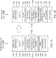
- FIGS. 1A and 1B are layer schematics, each showing a cross-section of a device comprising baseline and new III-V 3J solar cells 100A, 100B, respectively, and describing both a method of fabricating the device and a method of generating a current using the device.
- FIG. 1A shows the baseline III-V 3J solar cell 100A.
- the solar cell 100A includes a p-type doped germanium (p-Ge) substrate 102, upon which is deposited and/or fabricated a standard (std) nucleation layer 104, a buffer layer 106, a lower tunnel junction 108, a middle sub-cell (MC) back surface field (BSF) 110, a middle sub-cell 112A comprised of a base 114A and an emitter 116, wherein the base 114A is comprised of gallium indium arsenide (GaInAs) with p-type doping of about 1e14 cm -3 to 1e16 cm -3 , and having a thickness of about 3.5 ⁇ m and the emitter 116 is comprised of indium gallium arsenide (InGaAs), an MC window 118, a top tunnel junction 120, a top sub-cell (TC) BSF 122, a top sub-cell 124 comprised of
- the baseline solar cell 100A has a fully-absorbing middle sub-cell 112A base 114A with a thickness of about 3.5 ⁇ m.
- the middle sub-cell 112A base 114A p-type doping is low at about 1e14 cm -3 to 1e16 cm -3 , to increase the space charge region.
- the space charge region collects minority carriers regardless of reductions to the diffusion length of the middle sub-cell 112A caused by radiation damage.
- Such a layer design is optimized for radiation dose of about 1e15 e-/cm 2 or less.
- FIG. 1B shows the new III-V 3J solar cell 100B according to this disclosure, wherein a reflector 130, i.e., a DBR 130 comprised of aluminum gallium arsenide (AlGaAs) and gallium arsenide (GaAs), is inserted behind the middle sub-cell 112B positioned between the buffer layer 106 and the lower tunnel junction 108, and the DBR 130 has a reflectance centered at a wavelength of about 870 nm.
- the middle sub-cell 112B includes a base 114B comprised of GaInAs with a p-type doping of about 1e14 cm -3 to 1e16 cm -3 that has a thickness of about 2.1 ⁇ m. Otherwise, the structure of 100B is the same as the structure of 100A.
- the new solar cell 100B has two major changes from the baseline solar cell 100A, including a reduction in the middle sub-cell 112A base 114A of 3.5 ⁇ m to the middle sub-cell 112B base 114B thickness of 2.1 ⁇ m, and the addition of the DBR 130 with a center wavelength at 870 nm.
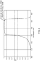
- FIG. 2 is a graph that shows the internal quantum efficiency curves for the baseline solar cell 100A with a 3.5 ⁇ m thick middle sub-cell 112A base 114A, and the new solar cell 100B with a 2.1 ⁇ m thick middle sub-cell 112B base 114B.
- the new solar cell 100B has an exceptional BOL efficiency.
- the BOL LIV characteristics for the new solar cell 100B are summarized in FIG. 3 .
- FIG. 3 shows four experimental splits for a comparison of LIV (light-current-voltage) data, including Voc (open current voltage), Jsc (short circuit current), Eff (solar cell efficiency at a maximum power point), and FF (fill factor) between the baseline and new solar cells.
- Voc open current voltage
- Jsc short circuit current
- Eff solar cell efficiency at a maximum power point
- FF fill factor
- the new solar cell 100B is nearly 70 mV higher than the baseline solar cell 100A.
- the current of the new solar cell 100B matches that of the baseline solar cell 100A.
- Overall BOL efficiency for the new solar cell 100B is 4% higher than the baseline solar cell 100A.
- the low p-type doping (about 1e14 cm -3 to 1e16 cm -3 ) of the middle sub-cell 112B base 114B in the new solar cell 100B and the thinness (about 2.1 ⁇ m) of the middle sub-cell 112B base 114B in the new solar cell 100B has significant benefits in EOL performance, particularly at high radiation levels.
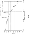
- a graph of power retention (NPmp) as a function of a 1 MeV electron radiation dose (e- dose) (e-/cm2) (electron fluence) for the baseline and new solar cells 100A, 100B is shown in FIG. 4 . From FIG. 4 , it is evident that the power retention of the new solar cell 100B is similar to the baseline solar cell 100A for the 1 MeV electron radiation dose from 0 to 5e14 e-/cm 2 .
- the 1 MeV electron radiation dose from about 1e15 e-/cm 2 to 1e16 e-/cm 2 , the NPmp of the new solar cell 100B is clearly greater than the baseline solar cell 100A, with the difference increasing with increasing radiation dose.
- the 1 MeV electron radiation doses of about 1e15 e-/cm 2 and 1e16 e-/cm 2 there is a 1% and 8% relative improvement in NPmp for the new solar cell 100B over the baseline solar cell 100A.
- EOL efficiency BOL efficiency x NPmp.
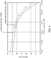
- a graph of EOL efficiency as a function of the 1 MeV electron radiation dose for the baseline and new solar cells 100A, 100B is shown FIG. 5 .
- the EOL efficiency of the new solar cell 100B is greater than the baseline solar cell 100A at all radiation doses.
- the difference in EOL efficiency is about 4%, due to the 4% advantage of the new solar cell 100B at BOL.
- the difference in EOL efficiency starts to increase above about 4% due to the superior NPmp values for the new solar cell 100B relative to the baseline solar cell 100A.
- the difference in EOL efficiency is about 12%. This is a significant increase in EOL efficiency that is unmatched by other solar cells offered in the marketplace.
- This disclosure is the first known solution that combines low p-type doping of a thin middle sub-cell 112B base 114B with a DBR 130 to optimize middle sub-cell 112B retention in high radiation environments. This results in at least two advantages.
- a middle sub-cell 112B base 114B having a thickness of about 2 to 3 ⁇ m, more preferably about 2.1 to 2.3 ⁇ m, and most preferably about 2.1 ⁇ m, combined with an effective DBR 130, in the new solar cell 100B results in an effective absorption length equal to a fully absorbing middle sub-cell 112A base 114A having a thickness of about 3 to 3.5 ⁇ m, without a DBR, in the baseline solar cell 100A.
- the BOL current of the middle sub-cell 112B in the new solar cell 100B, and hence the BOL efficiency of the new solar cell 100B is not compromised to improve EOL efficiency. Consequently, the new solar cell 100B is still able to achieve BOL efficiency levels of near 32% that are 4% relative above the current state-of-the-art baseline solar cell 100A.
- the relatively thinner middle sub-cell 112B base 114B in the new solar cell 100B combined with the low p-type doping of the middle sub-cell 112B base 114B in the new solar cell 100B, results in power retention with a radiation dose of about 1e15 e-/cm 2 to 1e16 e-/cm 2 that is unmatched in the industry.
- power retention and EOL power for the new solar cell 100B solution is 12% better than the current state-of-the-art baseline solar cell 100A at these radiation doses.
- the result of this disclosure is a new solar cell 100B design optimized for performance at high radiation doses that exhibits an EOL efficiency 12% better than present state-of-the-art baseline solar cell 100A designs after a MEO-like radiation dose of about 1e16 e-/cm 2 .
- this disclosure describes the widely adopted triple junction solar cell 100B, it could be broadened to cover any instance of a solar cell 100B comprising a single or multiple junction solar cell, e.g., single junction solar cells, double junction solar cells, or other multiple junction solar cells.
- middle sub-cell 112B is described as comprising InGaAs and GaInAs, and the DBR 130 is described as comprising AlGaAs and GaAs, other materials could also be used.
- middle sub-cell 112B, base 114B, and DBR 130 are described as comprising certain materials, alternatives may describe the middle sub-cell 112B, base 114B, and DBR 130 as consisting of, or consisting essentially of, these or other materials.
- this disclosure is applicable to inverted metamorphic (IMM) devices in any sub-cell to enhance the radiation retention of the devices.
- this disclosure may be applied to GaAs, GaInAs, AlGaAs, AlGaInAs, GaInAsSb, GaInAsN, GaInAsNSb, GaInAsSb, GaAsSb, GaPAsSb sub-cells within that architecture.
- reflectors other than DBRs 130 may be used to capture a second pass of light through the sub-cell 112B.
- Such reflectors may be embedded in the epitaxy, such as AlAs/GaAs, AlGaInAs/GaInAs, AlGaAsSb/GaAsSb and similar DBRs, or metal surfaces applied to the back of the sub-cell 112B, including low index materials, such as TiOx, SiOx, Al 2 O 3 coated with a metal layer such as Ag, Au, Al, Ti, Pt, Ni, or similar common metals in semiconductor device fabrication.
- the sub-cells have an n-on-p configuration as is usual for a p-type Ge substrate, which means that the emitter of the sub-cell is n-type and the base is p-type.
- other examples may comprise a p-on-n configuration, wherein the emitter of the sub-cell is p-type and the base is n-type.
- this disclosure describes the new solar cell 100B performing in a desired manner at a radiation dose of about 1eI5 e-/cm 2 to 1e16 e-/cm 2
- alternatives may describe the new solar cell 100B as performing in the desired manner at radiation doses greater than or less than the range of about 1e15 e-/cm 2 to 1e16 e-/cm 2 .
- Examples of the disclosure may be described in the context of a method 600 of fabricating a solar cell, solar cell panel and/or aerospace vehicle such as a satellite, comprising steps 602-614, as shown in FIG. 6A , wherein the resulting satellite 616 comprised of various systems 618 and a body 620, including a panel 622 comprised of an array 624 of one or more new solar cells 100B is shown in FIG. 6B .
- exemplary method 600 may include specification and design 602 of the satellite 616, and material procurement 604 for same.
- component and subassembly manufacturing 606 and system integration 608 of the satellite 616 takes place, which include fabricating the satellite 616, panel 622, array 624 and new solar cells 100B.
- the satellite 616 may go through certification and delivery 610 in order to be placed in service 612.
- the satellite 616 may also be scheduled for maintenance and service 614 (which includes modification, reconfiguration, refurbishment, and so on), before being launched.
- FIG. 7 is an illustration of the panel 622 in the form of a functional block diagram, according to one example.
- the panel 622 is comprised of the array 624, which is comprised of one or more of the new solar cells 100B individually attached to the panel 622.
- the solar cell 100B may comprise a single or multiple junction solar cell 100B, e.g., a single junction solar cell 100B, double junction solar cell 100B, or other multiple junction solar cell 100B.
Landscapes
- Photovoltaic Devices (AREA)
- Life Sciences & Earth Sciences (AREA)
- Engineering & Computer Science (AREA)
- Sustainable Energy (AREA)
- Sustainable Development (AREA)
Abstract
Description
- The disclosure is related generally to a solar cell design optimized for performance at high radiation doses.
- Until recently, space satellites operated in geosynchronous (GEO) orbits with total effective radiation dose of about 1e15 e-/cm2. Over the past few years, missions have diversified to include those middle earth orbits (MEO) with far higher effective radiation doses that are an order of magnitude higher than that of GEO. Therefore, solar cell performance in high radiation space environments is becoming increasingly critical.
- There have been previous methods to solve this problem. One such method is described in
U.S. Patent No. 9,252,313, issued February 2, 2016, to Matthias Meusel et al. - The '313 patent specifies the use of a semiconductor mirror disposed between two partial cells, with the thickness of the partial cell above the mirror cut in half by using the mirror, without drastically reducing the absorption of the partial cell. However, the design of the ' 313 patent falls off in performance quickly after high radiation doses of about 1e15 e-/cm2 or greater.
- Thus, there is a need for solar cell designs optimized for performance at high radiation doses.
- To overcome the limitations described above, and to overcome other limitations that will become apparent upon reading and understanding the present specification, the present disclosure describes a device, a method of fabricating the device, and a method of generating a current using the device, wherein the device is a solar cell optimized for performance at high radiation doses, and the solar cell includes: a sub-cell comprised of a base and an emitter; the base of the sub-cell has a thickness of about 2 to 3 µm; the base of the sub-cell is doped at about 1e14 cm-3 to 1e16 cm-3; and a reflector is inserted behind the sub-cell to maximize current generated by the sub-cell.
- Referring now to the drawings in which like reference numbers represent corresponding parts throughout:
-
FIGS. 1A and 1B are layer schematics of triple junction solar cells, whereinFIG. 1A is a baseline solar cell andFIG. 1B is a new solar cell. -
FIG. 2 is a graph of internal quantum efficiency (IQE) vs. Wavelength (nm) for the baseline and new solar cells. -
FIG. 3 shows four experimental splits for a comparison of LIV (light-current-voltage) data, including Voc (open current voltage), Jsc (short circuit current), Eff (solar cell efficiency at a maximum power point), and FF (fill factor) between the baseline and new solar cells. -
FIG. 4 is a graph of power retention (NPmp) vs. 1 MeV e- dose (e-/cm2) (electron fluence) for the baseline and new solar cells. -
FIG. 5 is a graph of end-of-life (EOL) efficiency (%) vs. 1 MeV e- dose (e-/cm2) (electron fluence) for the baseline and new solar cells. -
FIG. 6A illustrates a method of fabricating a solar cell, solar cell panel and/or satellite. -
FIG. 6B illustrates a resulting satellite having a solar cell panel comprised of solar cells. -
FIG. 7 is an illustration of the solar cell panel in the form of a functional block diagram. - In the following description, reference is made to the accompanying drawings which form a part hereof, and in which is shown by way of illustration a specific example in which the disclosure may be practiced. It is to be understood that other examples may be utilized and structural changes may be made without departing from the scope of the present disclosure.
- The power retention of a standard triple junction (3J) space solar cell following exposure to space radiation is most greatly affected by the retention of the GaAs middle cell (i.e., middle sub-cell). This disclosure significantly improves on the power retention of the middle sub-cell by reducing the thickness of the base of the middle sub-cell to less than that required to fully absorb light and lowering the doping of the base of the middle sub-cell.
- Preferably, the base of the middle sub-cell has a thickness of about 2 to 3 µm; more preferably the base of the middle sub-cell has a thickness of about 2.1 to 2.3 µm; and most preferably, the base of the middle sub-cell has a thickness of about 2.1 µm.
- Preferably, the base of the middle sub-cell is p-type doped at about 1e14 cm-3 to 1e16 cm-3.
- A reflector, such as a distributed Bragg reflector (DBR), is inserted behind the middle sub-cell to compensate for the reduced thickness of the middle sub-cell base and to maximize the current of the middle sub-cell. Preferably, the reflectance is centered at a wavelength of about 870 nm.
- Experimentally, beginning-of-life (BOL) solar cell efficiencies at 32% have been demonstrated using this disclosure that are 4% relative better than the current industry standard. Moreover, the end-of-life (EOL) power of the solar cell at high electron fluences of about 1e15 e-/cm2 to 1e16 e-/cm2 using this disclosure exceeds the previous state-of-the-art solar cell by 12% relative.
-
FIGS. 1A and 1B are layer schematics, each showing a cross-section of a device comprising baseline and new III-V 3Jsolar cells -
FIG. 1A shows the baseline III-V 3Jsolar cell 100A. Thesolar cell 100A includes a p-type doped germanium (p-Ge)substrate 102, upon which is deposited and/or fabricated a standard (std)nucleation layer 104, abuffer layer 106, alower tunnel junction 108, a middle sub-cell (MC) back surface field (BSF) 110, amiddle sub-cell 112A comprised of abase 114A and anemitter 116, wherein thebase 114A is comprised of gallium indium arsenide (GaInAs) with p-type doping of about 1e14 cm-3 to 1e16 cm-3, and having a thickness of about 3.5 µm and theemitter 116 is comprised of indium gallium arsenide (InGaAs), anMC window 118, atop tunnel junction 120, a top sub-cell (TC)BSF 122, atop sub-cell 124 comprised of GaInP, awindow 126 comprised of aluminum indium phosphide (AlInP), and acap 128 comprised of GaInAs. Thesolar cell 100A may include other features not illustrated, such as an anti-reflection coating, and front and back metal contacts. - The baseline
solar cell 100A has a fully-absorbingmiddle 114A with a thickness of about 3.5 µm. Thesub-cell 112A basemiddle 114A p-type doping is low at about 1e14 cm-3 to 1e16 cm-3, to increase the space charge region. The space charge region collects minority carriers regardless of reductions to the diffusion length of thesub-cell 112A basemiddle sub-cell 112A caused by radiation damage. Such a layer design is optimized for radiation dose of about 1e15 e-/cm2 or less. -
FIG. 1B shows the new III-V 3Jsolar cell 100B according to this disclosure, wherein areflector 130, i.e., aDBR 130 comprised of aluminum gallium arsenide (AlGaAs) and gallium arsenide (GaAs), is inserted behind themiddle sub-cell 112B positioned between thebuffer layer 106 and thelower tunnel junction 108, and theDBR 130 has a reflectance centered at a wavelength of about 870 nm. In addition, themiddle sub-cell 112B includes abase 114B comprised of GaInAs with a p-type doping of about 1e14 cm-3 to 1e16 cm-3 that has a thickness of about 2.1 µm. Otherwise, the structure of 100B is the same as the structure of 100A. - The new
solar cell 100B has two major changes from the baselinesolar cell 100A, including a reduction in themiddle 114A of 3.5 µm to thesub-cell 112A basemiddle 114B thickness of 2.1 µm, and the addition of thesub-cell 112B baseDBR 130 with a center wavelength at 870 nm. - The use of the DBR 130 allows the
middle 114B to be thinned down to about 2.1 µm without compromising the current generated by thesub-cell 112B basemiddle sub-cell 112B. This is demonstrated inFIG. 2 , which is a graph that shows the internal quantum efficiency curves for the baselinesolar cell 100A with a 3.5 µmthick middle 114A, and the newsub-cell 112A basesolar cell 100B with a 2.1 µmthick middle 114B.sub-cell 112B base - Despite the fact that that the new
solar cell 100B has amiddle 114B nearly half the thickness of thesub-cell 112B basemiddle 114A of the baselinesub-cell 112A basesolar cell 100A, the internal quantum efficiency (IQE) signatures are nearly identical and the integrated currents are the same within error. The thinner 2.1µm middle 114B for the newsub-cell 112B basesolar cell 100B also benefits the voltage of the newsolar cell 100B. The thicker 3.5µm middle 114A has dark current near the back of the baselinesub-cell 112A basesolar cell 100A, where light intensities are low. - Partially as a consequence of the
high middle sub-cell 112B current (from the DBR 130) andhigher middle sub-cell 112B voltage (due to themiddle 114B being thinner), the newsub-cell 112B basesolar cell 100B has an exceptional BOL efficiency. The BOL LIV characteristics for the newsolar cell 100B are summarized inFIG. 3 . -
FIG. 3 shows four experimental splits for a comparison of LIV (light-current-voltage) data, including Voc (open current voltage), Jsc (short circuit current), Eff (solar cell efficiency at a maximum power point), and FF (fill factor) between the baseline and new solar cells. Thedotted lines 300 show the corresponding values for current state-of-the-art baselinesolar cells 100A. - The new
solar cell 100B is nearly 70 mV higher than the baselinesolar cell 100A. The current of the newsolar cell 100B matches that of the baselinesolar cell 100A. Overall BOL efficiency for the newsolar cell 100B is 4% higher than the baselinesolar cell 100A. - The low p-type doping (about 1e14 cm-3 to 1e16 cm-3) of the middle
sub-cell 112B base 114B in the newsolar cell 100B and the thinness (about 2.1 µm) of the middlesub-cell 112B base 114B in the newsolar cell 100B has significant benefits in EOL performance, particularly at high radiation levels. A graph of power retention (NPmp) as a function of a 1 MeV electron radiation dose (e- dose) (e-/cm2) (electron fluence) for the baseline and newsolar cells FIG. 4 . FromFIG. 4 , it is evident that the power retention of the newsolar cell 100B is similar to the baselinesolar cell 100A for the 1 MeV electron radiation dose from 0 to 5e14 e-/cm2. - However, the 1 MeV electron radiation dose from about 1e15 e-/cm2 to 1e16 e-/cm2, the NPmp of the new
solar cell 100B is clearly greater than the baselinesolar cell 100A, with the difference increasing with increasing radiation dose. At the 1 MeV electron radiation doses of about 1e15 e-/cm2 and 1e16 e-/cm2, there is a 1% and 8% relative improvement in NPmp for the newsolar cell 100B over the baselinesolar cell 100A. - The combination of improved BOL efficiency and NPmp results in an improved EOL efficiency, where EOL efficiency = BOL efficiency x NPmp. A graph of EOL efficiency as a function of the 1 MeV electron radiation dose for the baseline and new
solar cells FIG. 5 . - From
FIG. 5 , it is clear that the EOL efficiency of the newsolar cell 100B is greater than the baselinesolar cell 100A at all radiation doses. At low doses, the difference in EOL efficiency is about 4%, due to the 4% advantage of the newsolar cell 100B at BOL. Starting at the 1 MeV electron radiation dose of about 1e15 e-/cm2, the difference in EOL efficiency starts to increase above about 4% due to the superior NPmp values for the newsolar cell 100B relative to the baselinesolar cell 100A. At the 1 MeV electron radiation dose of about 1e16 e-/cm2, the difference in EOL efficiency is about 12%. This is a significant increase in EOL efficiency that is unmatched by other solar cells offered in the marketplace. - This disclosure, is the first known solution that combines low p-type doping of a thin middle
sub-cell 112B base 114B with aDBR 130 to optimize middle sub-cell 112B retention in high radiation environments. This results in at least two advantages. - First, the use of a middle
sub-cell 112B base 114B having a thickness of about 2 to 3 µm, more preferably about 2.1 to 2.3 µm, and most preferably about 2.1 µm, combined with aneffective DBR 130, in the newsolar cell 100B, results in an effective absorption length equal to a fully absorbingmiddle 114A having a thickness of about 3 to 3.5 µm, without a DBR, in the baselinesub-cell 112A basesolar cell 100A. In this way, the BOL current of the middle sub-cell 112B in the newsolar cell 100B, and hence the BOL efficiency of the newsolar cell 100B, is not compromised to improve EOL efficiency. Consequently, the newsolar cell 100B is still able to achieve BOL efficiency levels of near 32% that are 4% relative above the current state-of-the-art baselinesolar cell 100A. - Second, the relatively thinner middle
sub-cell 112B base 114B in the newsolar cell 100B, combined with the low p-type doping of the middlesub-cell 112B base 114B in the newsolar cell 100B, results in power retention with a radiation dose of about 1e15 e-/cm2 to 1e16 e-/cm2 that is unmatched in the industry. As a result, power retention and EOL power for the newsolar cell 100B solution is 12% better than the current state-of-the-art baselinesolar cell 100A at these radiation doses. - The result of this disclosure is a new
solar cell 100B design optimized for performance at high radiation doses that exhibits anEOL efficiency 12% better than present state-of-the-art baselinesolar cell 100A designs after a MEO-like radiation dose of about 1e16 e-/cm2. - The description set forth above has been presented for purposes of illustration and description, and is not intended to be exhaustive or limited to the examples described. Many alternatives and modifications may be used in place of the specific description set forth above.
- For example, although this disclosure describes the widely adopted triple junction
solar cell 100B, it could be broadened to cover any instance of asolar cell 100B comprising a single or multiple junction solar cell, e.g., single junction solar cells, double junction solar cells, or other multiple junction solar cells. - In another example, although the middle sub-cell 112B is described as comprising InGaAs and GaInAs, and the
DBR 130 is described as comprising AlGaAs and GaAs, other materials could also be used. - In yet another example, although this disclosure describes the
middle sub-cell 112B,base 114B, andDBR 130 are described as comprising certain materials, alternatives may describe themiddle sub-cell 112B,base 114B, andDBR 130 as consisting of, or consisting essentially of, these or other materials. - In yet another example, this disclosure is applicable to inverted metamorphic (IMM) devices in any sub-cell to enhance the radiation retention of the devices. Specifically, this disclosure may be applied to GaAs, GaInAs, AlGaAs, AlGaInAs, GaInAsSb, GaInAsN, GaInAsNSb, GaInAsSb, GaAsSb, GaPAsSb sub-cells within that architecture.
- In yet another example, reflectors other than
DBRs 130 may be used to capture a second pass of light through the sub-cell 112B. Such reflectors may be embedded in the epitaxy, such as AlAs/GaAs, AlGaInAs/GaInAs, AlGaAsSb/GaAsSb and similar DBRs, or metal surfaces applied to the back of the sub-cell 112B, including low index materials, such as TiOx, SiOx, Al2O3 coated with a metal layer such as Ag, Au, Al, Ti, Pt, Ni, or similar common metals in semiconductor device fabrication. - Typically, the sub-cells have an n-on-p configuration as is usual for a p-type Ge substrate, which means that the emitter of the sub-cell is n-type and the base is p-type. However, other examples may comprise a p-on-n configuration, wherein the emitter of the sub-cell is p-type and the base is n-type.
- Similarly, although this disclosure describes the new
solar cell 100B performing in a desired manner at a radiation dose of about 1eI5 e-/cm2 to 1e16 e-/cm2, alternatives may describe the newsolar cell 100B as performing in the desired manner at radiation doses greater than or less than the range of about 1e15 e-/cm2 to 1e16 e-/cm2. - Examples of the disclosure may be described in the context of a
method 600 of fabricating a solar cell, solar cell panel and/or aerospace vehicle such as a satellite, comprising steps 602-614, as shown inFIG. 6A , wherein the resultingsatellite 616 comprised ofvarious systems 618 and abody 620, including apanel 622 comprised of anarray 624 of one or more newsolar cells 100B is shown inFIG. 6B . - As illustrated in
FIG. 6A , during pre-production,exemplary method 600 may include specification anddesign 602 of thesatellite 616, andmaterial procurement 604 for same. During production, component andsubassembly manufacturing 606 andsystem integration 608 of thesatellite 616 takes place, which include fabricating thesatellite 616,panel 622,array 624 and newsolar cells 100B. Thereafter, thesatellite 616 may go through certification anddelivery 610 in order to be placed inservice 612. Thesatellite 616 may also be scheduled for maintenance and service 614 (which includes modification, reconfiguration, refurbishment, and so on), before being launched. - Each of the processes of
method 600 may be performed or carried out by a system integrator, a third party, and/or an operator (e.g., a customer). For the purposes of this description, a system integrator may include without limitation any number of manufacturers and major-system subcontractors; a third party may include without limitation any number of venders, subcontractors, and suppliers; and an operator may be a satellite company, military entity, service organization, and so on. - As shown in
FIG. 6B , thesatellite 616 fabricated byexemplary method 600 may includevarious systems 618 and abody 620. Examples of thesystems 618 included with thesatellite 616 include, but are not limited to, one or more of apropulsion system 626, anelectrical system 628, acommunications system 630, and apower system 632. Any number of other systems also may be included. -
FIG. 7 is an illustration of thepanel 622 in the form of a functional block diagram, according to one example. Thepanel 622 is comprised of thearray 624, which is comprised of one or more of the newsolar cells 100B individually attached to thepanel 622. Thesolar cell 100B may comprise a single or multiple junctionsolar cell 100B, e.g., a single junctionsolar cell 100B, double junctionsolar cell 100B, or other multiple junctionsolar cell 100B. At least one of the newsolar cells 100B includes a sub-cell 112B comprised of abase 114B and anemitter 116, thebase 114B has a thickness of about 2 to 3 µm, thebase 114B is p-type doped at about 1e14 cm-3 to 1e16 cm-3, and aDBR 130 is inserted behind the sub-cell 112B to maximize current generated by the sub-cell 112B. Each of the newsolar cells 100B absorbs light 700 from alight source 702 and generates anelectrical output 704 in response thereto. - Further, the disclosure comprises examples according to the following clauses:
-
Clause 1. A device, comprising: a solar cell optimized for performance at high radiation doses, wherein the solar cell includes: a sub-cell comprised of a base and an emitter; the base of the sub-cell has a thickness of about 2 to 3 µm; the base of the sub-cell is doped at about 1e14 cm-3 to 1e16 cm-3; and a reflector is inserted behind the sub-cell to maximize current generated by the sub-cell. - Clause 2. The device of
Clause 1, wherein the high radiation doses comprise radiation doses of about 1e15 e-/cm2 to 1e16 e-/cm2. - Clause 3. The device of
Clause 1 or 2, wherein the solar cell is a single junction or multiple junction solar cell. - Clause 4. The device of any of Clauses 1-3, wherein the reflector is a distributed Bragg reflector comprised of aluminum gallium arsenide (AlGaAs) and gallium arsenide (GaAs).
- Clause 5. The device of any of Clauses 1-4, wherein the reflector is positioned between a buffer layer and a lower tunnel junction of the solar cell.
- Clause 6. The device of any of Clauses 1-5, wherein the reflector has a reflectance centered at a wavelength of about 870 nm.
- Clause 7. The device of any of Clauses 1-6, wherein the sub-cell is a middle sub-cell of the solar cell.
- Clause 8. The device of any of Clauses 1-7, wherein the emitter of the sub-cell is comprised of indium gallium arsenide (InGaAs).
- Clause 9. The device of any of Clauses 1-8, wherein the base of the sub-cell is comprised of gallium indium arsenide (GaInAs).
- Clause 10. The device of any of Clauses 1-9, wherein the base of the sub-cell has a thickness of about 2.1 to 2.3 µm.
-
Clause 11. The device of any of Clauses 1-10, wherein the base of the sub-cell has a thickness of about 2.1 µm. -
Clause 12. The device of any of Clauses 1-11, wherein the solar cell is optimized for performance at the high radiation doses as compared to a baseline solar cell having a thicker sub-cell base and no reflector. -
Clause 13. The device ofClause 12, wherein a power retention as a function of a 1 MeV electron radiation dose of the solar cell is similar to the baseline solar cell for the 1 MeV electron radiation dose from about 0 to 5e14 e-/cm2. -
Clause 14. The device ofClause 12, wherein a power retention as a function of a 1 MeV electron radiation dose of the solar cell is greater than the baseline solar cell for the 1 MeV electron radiation dose from about 1e15 e-/cm2 to 1e16 e-/cm2. -
Clause 15. The device of any of Clauses 12-14, wherein the beginning-of-life (BOL) efficiency of the solar cell is greater than the baseline solar cell at all radiation doses. -
Clause 16. The device of any of Clauses 12-15, wherein an end-of-life (EOL) efficiency of the solar cell is greater than the baseline solar cell at all radiation doses. - Clause 17. The device of any of Clauses 1-16, further comprising a panel including the solar cell.
- Clause 18. The device of Clause 17, further comprising a space vehicle including the panel.
-
Clause 19. A method, comprising: fabricating a solar cell optimized for performance at high radiation doses, wherein the solar cell includes: a sub-cell comprised of a base and an emitter; the base of the sub-cell has a thickness of about 2 to 3 µm; the base of the sub-cell is doped at about 1e14 cm-3 to 1e16 cm-3; and a reflector is inserted behind the sub-cell to maximize current generated by the sub-cell. - Clause 20. A method, comprising: generating a current using a solar cell optimized for performance at high radiation doses, wherein the solar cell includes: a sub-cell comprised of a base and an emitter; the base of the sub-cell has a thickness of about 2 to 3 µm; the base of the sub-cell is doped at about 1e14 cm3 to 1e16 cm-3; and a reflector is inserted behind the sub-cell to maximize current generated by the sub-cell.
Claims (15)
- A device, comprising:
a solar cell (100B) optimized for performance at high radiation doses, wherein the solar cell (100B) includes:a sub-cell (112B) comprised of a base (114B) and an emitter (116);the base (114B) of the sub-cell (112B) has a thickness of about 2 to 3 µm;the base (114B) of the sub-cell (112B) is doped at about 1e14 cm-3 to 1e16 cm-3; anda reflector (130) is inserted behind the sub-cell (112B) to maximize current generated by the sub-cell (112B). - The device of claim 1, wherein the high radiation doses comprise radiation doses of about 1e15 e-/cm2 to 1e16 e-/cm2.
- The device of claim 1 or 2, wherein the reflector (130) is a distributed Bragg reflector (130) comprised of aluminum gallium arsenide (AlGaAs) and gallium arsenide (GaAs).
- The device of any of claims 1-3, wherein the reflector (130) is positioned between a buffer layer (106) and a lower tunnel junction (108) of the solar cell (100B).
- The device of any of claims 1-4, wherein the reflector (130) has a reflectance centered at a wavelength of about 870 nm.
- The device of any of claims 1-5, wherein the sub-cell (112B) is a middle sub-cell (112B) of the solar cell (100B).
- The device of any of claims 1-6, wherein the emitter (116) of the sub-cell (112B) is comprised of indium gallium arsenide (InGaAs).
- The device of any of claims 1-7, wherein the base (114B) of the sub-cell (112B) is comprised of gallium indium arsenide (GaInAs).
- The device of any of claims 1-8, wherein the base (114B) of the sub-cell (112B) has a thickness of about 2.1 to 2.3 µm.
- The device of any of claims 1-9, wherein the solar cell (100B) is optimized for performance at the high radiation doses as compared to a baseline solar cell (100A) having a thicker sub-cell (112A) base (114A) and no reflector (130).
- The device of claim 10, wherein a power retention as a function of a 1 MeV electron radiation dose of the solar cell (100B) is similar to the baseline solar cell (100A) for the 1 MeV electron radiation dose from about 0 to 5e14 e-/cm2 and/or wherein a power retention as a function of a 1 MeV electron radiation dose of the solar cell (100B) is greater than the baseline solar cell (100A) for the 1 MeV electron radiation dose from about 1e15 e-/cm2 to 1e16 e-/cm2.
- The device of claim 10 or 11, wherein the beginning-of-life (BOL) efficiency of the solar cell (100B) is greater than the baseline solar cell (100A) at all radiation doses and/or wherein an end-of-life (EOL) efficiency of the solar cell (100B) is greater than the baseline solar cell (100A) at all radiation doses.
- The device of any of claims 1-12, further comprising a panel (622) including the solar cell (100B), the device preferably further comprising a space vehicle (616) including the panel (622).
- A method, comprising:
fabricating (600-614) a solar cell (100B) optimized for performance at high radiation doses, wherein the solar cell (100B) includes:a sub-cell (112B) comprised of a base (114B) and an emitter (116);the base (114B) of the sub-cell (112B) has a thickness of about 2 to 3 µm;the base (114B) of the sub-cell (112B) is doped at about 1e14 cm-3 to 1e16 cm-3; anda reflector (130) is inserted behind the sub-cell (112B) to maximize current generated by the sub-cell (112B). - A method, comprising:
generating (704) a current using a solar cell (100B) optimized for performance at high radiation doses, wherein the solar cell (100B) includes:a sub-cell (112B) comprised of a base (114B) and an emitter (116);the base (114B) of the sub-cell (112B) has a thickness of about 2 to 3 µm;the base (114B) of the sub-cell (112B) is doped at about 1e14 cm-3 to 1e16 cm-3; anda reflector (130) is inserted behind the sub-cell (112B) to maximize current generated by the sub-cell (112B).
Applications Claiming Priority (1)
| Application Number | Priority Date | Filing Date | Title |
|---|---|---|---|
| US16/452,083 US20200411708A1 (en) | 2019-06-25 | 2019-06-25 | Solar cell design optimized for performance at high radiation doses |
Publications (1)
| Publication Number | Publication Date |
|---|---|
| EP3758072A1 true EP3758072A1 (en) | 2020-12-30 |
Family
ID=70227840
Family Applications (1)
| Application Number | Title | Priority Date | Filing Date |
|---|---|---|---|
| EP20168452.9A Pending EP3758072A1 (en) | 2019-06-25 | 2020-04-07 | Solar cell design optimized for performance at high radiation doses |
Country Status (4)
| Country | Link |
|---|---|
| US (1) | US20200411708A1 (en) |
| EP (1) | EP3758072A1 (en) |
| JP (1) | JP2021013013A (en) |
| CN (1) | CN112133776A (en) |
Families Citing this family (3)
| Publication number | Priority date | Publication date | Assignee | Title |
|---|---|---|---|---|
| CN112713205A (en) * | 2021-03-29 | 2021-04-27 | 南昌凯迅光电有限公司 | High-radiation-resistance triple-junction gallium arsenide solar cell and preparation method thereof |
| CN112864282B (en) * | 2021-04-23 | 2021-11-05 | 南昌凯迅光电有限公司 | Preparation method of anti-irradiation efficient gallium arsenide solar cell |
| CN113690335B (en) * | 2021-10-26 | 2022-03-08 | 南昌凯迅光电股份有限公司 | An improved triple-junction gallium arsenide solar cell and its fabrication method |
Citations (2)
| Publication number | Priority date | Publication date | Assignee | Title |
|---|---|---|---|---|
| CN104617168A (en) * | 2014-12-26 | 2015-05-13 | 天津蓝天太阳科技有限公司 | Radiation-proof three-junction cascade gallium arsenide solar cell and preparation method |
| US9252313B2 (en) | 2005-01-04 | 2016-02-02 | Azur Space Solar Power Gmbh | Monolithic multiple solar cells |
Family Cites Families (9)
| Publication number | Priority date | Publication date | Assignee | Title |
|---|---|---|---|---|
| US8609984B2 (en) * | 2009-06-24 | 2013-12-17 | Florida State University Research Foundation, Inc. | High efficiency photovoltaic cell for solar energy harvesting |
| US10170652B2 (en) * | 2011-03-22 | 2019-01-01 | The Boeing Company | Metamorphic solar cell having improved current generation |
| US20140182667A1 (en) * | 2013-01-03 | 2014-07-03 | Benjamin C. Richards | Multijunction solar cell with low band gap absorbing layer in the middle cell |
| EP3329521B1 (en) * | 2015-07-27 | 2022-07-06 | Sierra Space Corporation | Solar array system and method of manufacturing |
| US20170092800A1 (en) * | 2015-08-17 | 2017-03-30 | Solaero Technologies Corp. | Four junction inverted metamorphic solar cell |
| JP6404282B2 (en) * | 2015-08-17 | 2018-10-10 | ソレアロ テクノロジーズ コーポレイション | Multijunction inverted metamorphic solar cell |
| US20170054048A1 (en) * | 2015-08-17 | 2017-02-23 | Solaero Technologies Corp. | Four junction solar cell for space applications |
| US10541345B2 (en) * | 2016-01-12 | 2020-01-21 | The Boeing Company | Structures for increased current generation and collection in solar cells with low absorptance and/or low diffusion length |
| WO2019010037A1 (en) * | 2017-07-06 | 2019-01-10 | Solar Junction Corporation | Hybrid mocvd/mbe epitaxial growth of high-efficiency lattice-matched multijunction solar cells |
-
2019
- 2019-06-25 US US16/452,083 patent/US20200411708A1/en not_active Abandoned
-
2020
- 2020-04-07 EP EP20168452.9A patent/EP3758072A1/en active Pending
- 2020-04-24 CN CN202010332722.2A patent/CN112133776A/en active Pending
- 2020-04-25 JP JP2020077855A patent/JP2021013013A/en active Pending
Patent Citations (2)
| Publication number | Priority date | Publication date | Assignee | Title |
|---|---|---|---|---|
| US9252313B2 (en) | 2005-01-04 | 2016-02-02 | Azur Space Solar Power Gmbh | Monolithic multiple solar cells |
| CN104617168A (en) * | 2014-12-26 | 2015-05-13 | 天津蓝天太阳科技有限公司 | Radiation-proof three-junction cascade gallium arsenide solar cell and preparation method |
Non-Patent Citations (7)
| Title |
|---|
| ANDREEV V. M. ET AL: "Radiation Degradation of Multijunction III-V Solar Cells and Prediction of their Lifetime", PROCEEDINGS OF THE 27TH EUROPEAN PHOTOVOLTAIC SOLAR ENERGY CONFERENCE, 25 September 2012 (2012-09-25) - 28 September 2012 (2012-09-28), pages 169 - 174, XP040633711, ISBN: 978-3-936338-28-7 * |
| EMELYANOV V M ET AL: "Multijunction GaInP/GaInAs/Ge solar cells with Bragg reflectors", SEMICONDUCTORS, NAUKA/INTERPERIODICA, MO, vol. 44, no. 12, 30 December 2010 (2010-12-30), pages 1600 - 1605, XP019855566, ISSN: 1090-6479, DOI: 10.1134/S1063782610120122 * |
| MELLOR A ET AL: "Interstitial light-trapping design for multi-junction solar cells", SOLAR ENERGY MATERIALS AND SOLAR CELLS, ELSEVIER SCIENCE PUBLISHERS, AMSTERDAM, NL, vol. 159, 20 September 2016 (2016-09-20), pages 212 - 218, XP029788572, ISSN: 0927-0248, DOI: 10.1016/J.SOLMAT.2016.09.005 * |
| POLLY STEPHEN J ET AL: "Radiation Effects in Thinned GaAs Photovoltaics Incorporating DBRs for Improved Radiation Tolerance of Multijunctions", 2019 IEEE 46TH PHOTOVOLTAIC SPECIALISTS CONFERENCE (PVSC), IEEE, 16 June 2019 (2019-06-16), pages 2818 - 2821, XP033706428, DOI: 10.1109/PVSC40753.2019.8980875 * |
| SHVARTS M Z ET AL: "Radiation resistant AlGaAs/GaAs concentrator solar cells with internal Bragg reflector", SOLAR ENERGY MATERIALS AND SOLAR CELLS, ELSEVIER SCIENCE PUBLISHERS, AMSTERDAM, NL, vol. 68, no. 1, April 2001 (2001-04-01), pages 105 - 122, XP004226971, ISSN: 0927-0248, DOI: 10.1016/S0927-0248(00)00349-4 * |
| SKACHKOV A F: "Optimization of the structure of a GaInP/GaAs/Ge triple-junction solar cell with an Al0.1Ga0.9As/Al0.8Ga0.2As integrated bragg reflector", OPTOELECTRONICS, INSTRUMENTATION AND DATA PROCESSING, PLEIADES PUBLISHING, MOSCOW, vol. 50, no. 4, 24 September 2014 (2014-09-24), pages 423 - 427, XP035397266, ISSN: 8756-6990, [retrieved on 20140924], DOI: 10.3103/S8756699014040165 * |
| ZHANG LEI ET AL: "Investigation on high-efficiency Ga0.51In0.49P/In0.01Ga0.99As/Ge triple-junction solar cells for space applications", AIP ADVANCES, AMERICAN INSTITUTE OF PHYSICS, 2 HUNTINGTON QUADRANGLE, MELVILLE, NY 11747, vol. 7, no. 12, 14 December 2017 (2017-12-14), XP012224547, DOI: 10.1063/1.5006865 * |
Also Published As
| Publication number | Publication date |
|---|---|
| US20200411708A1 (en) | 2020-12-31 |
| JP2021013013A (en) | 2021-02-04 |
| CN112133776A (en) | 2020-12-25 |
Similar Documents
| Publication | Publication Date | Title |
|---|---|---|
| CN106887481B (en) | Multi-junction solar cells | |
| EP2641275B1 (en) | TYPE-II HIGH BANDGAP TUNNEL JUNCTIONS OF InP LATTICE CONSTANT FOR MULTIJUNCTION SOLAR CELLS | |
| US9257586B2 (en) | Monolithic multiple solar cells | |
| US10714636B2 (en) | Method for forming a multijunction metamorphic solar cell for space applications | |
| US20210305448A1 (en) | Multijunction metamorphic solar cells | |
| US20180240922A1 (en) | Four junction solar cell and solar cell assemblies for space applications | |
| US20200027999A1 (en) | Multijunction solar cell and solar cell assemblies for space applications | |
| EP3758072A1 (en) | Solar cell design optimized for performance at high radiation doses | |
| JP2000332282A (en) | Two-layer passivation structure for photovoltaic cells | |
| EP3167491B1 (en) | Compound-semiconductor photovoltaic cell and manufacturing method of compound-semiconductor photovoltaic cell | |
| EP3159939B1 (en) | Multijunction solar cell assemblies for space applications | |
| EP4036992B1 (en) | Four junction solar cell and solar cell assemblies for space applications | |
| US20200274016A1 (en) | MULTIJUNCTION SOLAR CELLS ON BULK GeSi SUBSTRATE | |
| EP3159943B1 (en) | Multijunction metamorphic solar cell for space applications | |
| WO2019175651A1 (en) | GaAs THREE-JUNCTION SOLAR CELL AND METHOD OF PREPARING THEREOF | |
| US11145776B2 (en) | Multijunction metamorphic solar cell for space applications | |
| US10256359B2 (en) | Lattice matched multijunction solar cell assemblies for space applications | |
| US20220149211A1 (en) | Multijunction solar cell assembly | |
| US20020139417A1 (en) | Space solar cell | |
| Andreev et al. | Concentrator tandem solar cells based on AlGaAs/GaAs-InP/InGaAs (or GaSb) structures | |
| US12593514B2 (en) | Solar cell design for improved performance at low temperature |
Legal Events
| Date | Code | Title | Description |
|---|---|---|---|
| PUAI | Public reference made under article 153(3) epc to a published international application that has entered the european phase |
Free format text: ORIGINAL CODE: 0009012 |
|
| STAA | Information on the status of an ep patent application or granted ep patent |
Free format text: STATUS: THE APPLICATION HAS BEEN PUBLISHED |
|
| AK | Designated contracting states |
Kind code of ref document: A1 Designated state(s): AL AT BE BG CH CY CZ DE DK EE ES FI FR GB GR HR HU IE IS IT LI LT LU LV MC MK MT NL NO PL PT RO RS SE SI SK SM TR |
|
| AX | Request for extension of the european patent |
Extension state: BA ME |
|
| STAA | Information on the status of an ep patent application or granted ep patent |
Free format text: STATUS: REQUEST FOR EXAMINATION WAS MADE |
|
| 17P | Request for examination filed |
Effective date: 20210604 |
|
| RBV | Designated contracting states (corrected) |
Designated state(s): AL AT BE BG CH CY CZ DE DK EE ES FI FR GB GR HR HU IE IS IT LI LT LU LV MC MK MT NL NO PL PT RO RS SE SI SK SM TR |
|
| STAA | Information on the status of an ep patent application or granted ep patent |
Free format text: STATUS: EXAMINATION IS IN PROGRESS |
|
| 17Q | First examination report despatched |
Effective date: 20230111 |
|
| RAP3 | Party data changed (applicant data changed or rights of an application transferred) |
Owner name: THE BOEING COMPANY |