EP3757668B1 - Anzeigevorrichtung - Google Patents
Anzeigevorrichtung Download PDFInfo
- Publication number
- EP3757668B1 EP3757668B1 EP20181422.5A EP20181422A EP3757668B1 EP 3757668 B1 EP3757668 B1 EP 3757668B1 EP 20181422 A EP20181422 A EP 20181422A EP 3757668 B1 EP3757668 B1 EP 3757668B1
- Authority
- EP
- European Patent Office
- Prior art keywords
- display device
- disposed
- openings
- support member
- display panel
- Prior art date
- Legal status (The legal status is an assumption and is not a legal conclusion. Google has not performed a legal analysis and makes no representation as to the accuracy of the status listed.)
- Active
Links
Images





Classifications
-
- G—PHYSICS
- G09—EDUCATION; CRYPTOGRAPHY; DISPLAY; ADVERTISING; SEALS
- G09F—DISPLAYING; ADVERTISING; SIGNS; LABELS OR NAME-PLATES; SEALS
- G09F9/00—Indicating arrangements for variable information in which the information is built-up on a support by selection or combination of individual elements
- G09F9/30—Indicating arrangements for variable information in which the information is built-up on a support by selection or combination of individual elements in which the desired character or characters are formed by combining individual elements
- G09F9/301—Indicating arrangements for variable information in which the information is built-up on a support by selection or combination of individual elements in which the desired character or characters are formed by combining individual elements flexible foldable or roll-able electronic displays, e.g. thin LCD, OLED
-
- G—PHYSICS
- G02—OPTICS
- G02F—OPTICAL DEVICES OR ARRANGEMENTS FOR THE CONTROL OF LIGHT BY MODIFICATION OF THE OPTICAL PROPERTIES OF THE MEDIA OF THE ELEMENTS INVOLVED THEREIN; NON-LINEAR OPTICS; FREQUENCY-CHANGING OF LIGHT; OPTICAL LOGIC ELEMENTS; OPTICAL ANALOGUE/DIGITAL CONVERTERS
- G02F1/00—Devices or arrangements for the control of the intensity, colour, phase, polarisation or direction of light arriving from an independent light source, e.g. switching, gating or modulating; Non-linear optics
- G02F1/01—Devices or arrangements for the control of the intensity, colour, phase, polarisation or direction of light arriving from an independent light source, e.g. switching, gating or modulating; Non-linear optics for the control of the intensity, phase, polarisation or colour
- G02F1/13—Devices or arrangements for the control of the intensity, colour, phase, polarisation or direction of light arriving from an independent light source, e.g. switching, gating or modulating; Non-linear optics for the control of the intensity, phase, polarisation or colour based on liquid crystals, e.g. single liquid crystal display cells
- G02F1/133—Constructional arrangements; Operation of liquid crystal cells; Circuit arrangements
- G02F1/1333—Constructional arrangements; Manufacturing methods
- G02F1/133305—Flexible substrates, e.g. plastics, organic film
-
- B—PERFORMING OPERATIONS; TRANSPORTING
- B32—LAYERED PRODUCTS
- B32B—LAYERED PRODUCTS, i.e. PRODUCTS BUILT-UP OF STRATA OF FLAT OR NON-FLAT, e.g. CELLULAR OR HONEYCOMB, FORM
- B32B7/00—Layered products characterised by the relation between layers; Layered products characterised by the relative orientation of features between layers, or by the relative values of a measurable parameter between layers, i.e. products comprising layers having different physical, chemical or physicochemical properties; Layered products characterised by the interconnection of layers
- B32B7/04—Interconnection of layers
- B32B7/12—Interconnection of layers using interposed adhesives or interposed materials with bonding properties
-
- G—PHYSICS
- G06—COMPUTING OR CALCULATING; COUNTING
- G06F—ELECTRIC DIGITAL DATA PROCESSING
- G06F1/00—Details not covered by groups G06F3/00 - G06F13/00 and G06F21/00
- G06F1/16—Constructional details or arrangements
- G06F1/1613—Constructional details or arrangements for portable computers
- G06F1/1633—Constructional details or arrangements of portable computers not specific to the type of enclosures covered by groups G06F1/1615 - G06F1/1626
- G06F1/1637—Details related to the display arrangement, including those related to the mounting of the display in the housing
- G06F1/1641—Details related to the display arrangement, including those related to the mounting of the display in the housing the display being formed by a plurality of foldable display components
-
- G—PHYSICS
- G06—COMPUTING OR CALCULATING; COUNTING
- G06F—ELECTRIC DIGITAL DATA PROCESSING
- G06F1/00—Details not covered by groups G06F3/00 - G06F13/00 and G06F21/00
- G06F1/16—Constructional details or arrangements
- G06F1/1613—Constructional details or arrangements for portable computers
- G06F1/1633—Constructional details or arrangements of portable computers not specific to the type of enclosures covered by groups G06F1/1615 - G06F1/1626
- G06F1/1637—Details related to the display arrangement, including those related to the mounting of the display in the housing
- G06F1/1652—Details related to the display arrangement, including those related to the mounting of the display in the housing the display being flexible, e.g. mimicking a sheet of paper, or rollable
-
- H—ELECTRICITY
- H10—SEMICONDUCTOR DEVICES; ELECTRIC SOLID-STATE DEVICES NOT OTHERWISE PROVIDED FOR
- H10K—ORGANIC ELECTRIC SOLID-STATE DEVICES
- H10K77/00—Constructional details of devices covered by this subclass and not covered by groups H10K10/80, H10K30/80, H10K50/80 or H10K59/80
- H10K77/10—Substrates, e.g. flexible substrates
- H10K77/111—Flexible substrates
-
- B—PERFORMING OPERATIONS; TRANSPORTING
- B32—LAYERED PRODUCTS
- B32B—LAYERED PRODUCTS, i.e. PRODUCTS BUILT-UP OF STRATA OF FLAT OR NON-FLAT, e.g. CELLULAR OR HONEYCOMB, FORM
- B32B2457/00—Electrical equipment
- B32B2457/20—Displays, e.g. liquid crystal displays, plasma displays
-
- G—PHYSICS
- G02—OPTICS
- G02F—OPTICAL DEVICES OR ARRANGEMENTS FOR THE CONTROL OF LIGHT BY MODIFICATION OF THE OPTICAL PROPERTIES OF THE MEDIA OF THE ELEMENTS INVOLVED THEREIN; NON-LINEAR OPTICS; FREQUENCY-CHANGING OF LIGHT; OPTICAL LOGIC ELEMENTS; OPTICAL ANALOGUE/DIGITAL CONVERTERS
- G02F2201/00—Constructional arrangements not provided for in groups G02F1/00 - G02F7/00
- G02F2201/50—Protective arrangements
- G02F2201/503—Arrangements improving the resistance to shock
-
- H—ELECTRICITY
- H10—SEMICONDUCTOR DEVICES; ELECTRIC SOLID-STATE DEVICES NOT OTHERWISE PROVIDED FOR
- H10K—ORGANIC ELECTRIC SOLID-STATE DEVICES
- H10K2102/00—Constructional details relating to the organic devices covered by this subclass
- H10K2102/301—Details of OLEDs
- H10K2102/311—Flexible OLED
-
- H—ELECTRICITY
- H10—SEMICONDUCTOR DEVICES; ELECTRIC SOLID-STATE DEVICES NOT OTHERWISE PROVIDED FOR
- H10K—ORGANIC ELECTRIC SOLID-STATE DEVICES
- H10K59/00—Integrated devices, or assemblies of multiple devices, comprising at least one organic light-emitting element covered by group H10K50/00
- H10K59/10—OLED displays
- H10K59/12—Active-matrix OLED [AMOLED] displays
-
- Y—GENERAL TAGGING OF NEW TECHNOLOGICAL DEVELOPMENTS; GENERAL TAGGING OF CROSS-SECTIONAL TECHNOLOGIES SPANNING OVER SEVERAL SECTIONS OF THE IPC; TECHNICAL SUBJECTS COVERED BY FORMER USPC CROSS-REFERENCE ART COLLECTIONS [XRACs] AND DIGESTS
- Y02—TECHNOLOGIES OR APPLICATIONS FOR MITIGATION OR ADAPTATION AGAINST CLIMATE CHANGE
- Y02E—REDUCTION OF GREENHOUSE GAS [GHG] EMISSIONS, RELATED TO ENERGY GENERATION, TRANSMISSION OR DISTRIBUTION
- Y02E10/00—Energy generation through renewable energy sources
- Y02E10/50—Photovoltaic [PV] energy
- Y02E10/549—Organic PV cells
Definitions
- Exemplary embodiments relate generally to a display device and, more particularly, to a flexible display device.
- EP 3 493 288 A1 describes an adhesive provided by patterning a metal plate with a predetermined elastic modulus, wherein the adhesive is compressively deformed in response to an operation of an adherent to be folded, so that the adhesive can easily return to an original state thereof through formation of a plurality of inner neutral planes upon deformation.
- CN 109 545 087 A describes a foldable backboard structure and display device.
- CN 108 665 804 A describes a foldable electronic paper display device and a manufacturing method of the foldable electronic paper display device.
- KR 2017 0063344 A describes a foldable display device.
- CN 107 437 378 A describes a flexible display module.
- CN 109 036 133 A describes a backboard and a display assembly.
- US 2018/307338 A1 describes a display apparatus including a display module configured to display an image and to be folded about a folding axis at a folding area defined on a plane, a support member below the display module, and a protective member between the display module and the support member.
- Flat panel display devices are used as display devices and replacing a cathode ray tube display device due to lightweight and thin characteristics thereof.
- Flat panel display devices may include a liquid crystal display device and an organic light emitting diode display device, for example.
- a lower substrate and an upper substrate of a display panel included the display device may include a flexible material, such that a portion of the display panel may be bent or folded.
- the lower substrate included in the display panel may be formed of a polyimide substrate, and the upper substrate included in the display panel may have a thin film encapsulation structure.
- the flexible display devices may display an image even in a portion where the display panel is folded.
- the flexible display device may include a display area, in which an image is displayed, and a portion of the display area may be folded.
- the flexible display device may further include a support member disposed on a bottom surface of the display panel and including a plurality of openings. The openings of the support member may overlap the portion where the display panel is folded.
- the flexible display device may have defects at the folded portion.
- the illustrated exemplary embodiments are to be understood as providing exemplary features of varying detail of some ways in which the inventive concepts may be implemented in practice. Therefore, unless otherwise specified, the features, components, modules, layers, films, panels, regions, and/or aspects, etc. (hereinafter individually or collectively referred to as "elements"), of the various embodiments may be otherwise combined, separated, interchanged, and/or rearranged without departing from the inventive concepts.
- an element such as a layer
- it may be directly on, connected to, or coupled to the other element or layer or intervening elements or layers may be present.
- an element or layer is referred to as being “directly on,” “directly connected to,” or “directly coupled to” another element or layer, there are no intervening elements or layers present.
- the term “connected” may refer to physical, electrical, and/or fluid connection, with or without intervening elements.
- the D1-axis, the D2-axis, and the D3-axis are not limited to three axes of a rectangular coordinate system, such as the x, y, and z - axes, and may be interpreted in a broader sense.
- the D1-axis, the D2-axis, and the D3-axis may be perpendicular to one another, or may represent different directions that are not perpendicular to one another.
- X, Y, and Z and "at least one selected from the group consisting of X, Y, and Z” may be construed as X only, Y only, Z only, or any combination of two or more of X, Y, and Z, such as, for instance, XYZ, XYY, YZ, and ZZ.
- the term “and/or” includes any and all combinations of one or more of the associated listed items.
- Spatially relative terms such as “beneath,” “below,” “under,” “lower,” “above,” “upper,” “over,” “higher,” “side” (e.g., as in “sidewall”), and the like, may be used herein for descriptive purposes, and, thereby, to describe one elements relationship to another element(s) as illustrated in the drawings.
- Spatially relative terms are intended to encompass different orientations of an apparatus in use, operation, and/or manufacture in addition to the orientation depicted in the drawings. For example, if the apparatus in the drawings is turned over, elements described as “below” or “beneath” other elements or features would then be oriented “above” the other elements or features.
- the exemplary term “below” can encompass both an orientation of above and below.
- the apparatus may be otherwise oriented (e.g., rotated 90 degrees or at other orientations), and, as such, the spatially relative descriptors used herein interpreted accordingly.
- FIG. 1 is a plan view of a display device.
- FIG. 2 is a perspective view showing a folded shape of a display panel included in the display device of FIG. 1 .
- FIG. 3 is a cross-sectional view taken along line I-I' of FIG. 1 .
- FIG. 4 is an enlarged cross-sectional view showing region A of the display device of FIG. 1 .
- FIGS. 1 and 3 show a state in which a display device 100 is unfolded.
- the display device 100 may include a display panel 200, a shock absorbing member 410, a support member 500, an elastic member 430, a step difference compensation member 460, and the like.
- the display device 100 may include a display area 10 and a foldable area 20.
- the display area 10 is an area where an image is displayed from the display panel 200
- the foldable area 20 is an area where the display device 100 is folded or unfolded. A portion of the display area 10 may be defined in the foldable area 20.
- the step difference compensation member 460 may include a first step difference compensation member 461 and a second step difference compensation member 462.
- a plurality of openings 535, a plurality of protrusions 530, and a plurality of trenches 520 may be formed in the support member 500.
- the display panel 200 may be provided.
- the display panel 200 may include a plurality of sub-pixels, and may display an image through the sub-pixels.
- the display panel 200 may have a first surface S1 on which an image is displayed, and a second surface S2 facing the first surface S1.
- the display panel 200 may have a first side surface SS1 and a second side surface SS2 facing the first side surface SS1.
- the first side surface SS1 and the second side surface SS2 may become adjacent to each other.
- the display panel 200 located in the foldable area 20 may have a curved shape.
- the first surface S1 may be located on an inner side
- the second surface S2 may be located on an outer side
- the display panel 200 may be folded, such that the first surface S1 is located on the outer side and the second surface S2 is located on the inner side.
- the shock absorbing member 410 may be disposed on the second surface S2 of the display panel 200.
- the shock absorbing member 410 may be disposed between the support member 500 and the display panel 200.
- the shock absorbing member 410 may protect the display panel 200 from an external impact.
- the shock absorbing member 410 may include a flexible material so that the display panel 200 may be easily folded.
- the shock absorbing member 410 may include a material in the form of a foam, such as a polyurethane foam, a polystyrene foam, or the like.
- the support member 500 may be disposed on a bottom surface of the shock absorbing member 410.
- the support member 500 may be disposed on the second surface S2 of the display panel 200, and may include a plurality of openings 535 formed in the foldable area 20.
- the openings 535 may include openings 531 arranged in a first direction D1 parallel to a top surface of the display device 100, and openings 532 shifted in a second direction D2 orthogonal to the first direction D1 and arranged in the first direction D1.
- the support member 500 may further include a plurality of protrusions 530 protruding in a third direction D3 opposite to the second direction D2.
- a space between two adjacent protrusions among the protrusions 530 may define a trench 520.
- the openings 535 may include first to n th openings (where n is an integer of 1 or more) arranged in the first direction D1, and a k th opening (where k is an even number between 1 and n) among the first to n th openings may be located at a position shifted in a second direction perpendicular to the first direction.
- the support member 500 may further include protrusions 530 located in the third direction D3 with respect to each of (k-1) th and (k+1) th openings among the first to n th openings, and the trench 520 may be defined by the protrusions 530.
- the support member 500 may support the display panel 200, and may also assist the display panel 200 to be folded.
- the support member 500 may be disposed over the second surface S2 of the display panel 200 to support the display panel 200, and the openings 535 formed in the foldable area 20 may assist the display panel 200 to be folded.
- the openings 535 may be configured as an empty space.
- a shape of each of the openings 535 may be deformed.
- the support member 500 located in the foldable area 20 may be deformed in a longitudinal direction (e.g., first direction D1) without being deformed in a depth direction (e.g., a direction from the support member 500 toward the display panel 200).
- the support member 500 may include metal or plastic having a relatively large elastic force or a relatively large restoring force.
- the support member 500 may include steel use stainless (SUS).
- the support member 500 may include alloys (e.g., superelastic metals), such as nickel-titanium (Ni-Ti), nickel-aluminum (Ni-Al), copper-zinc-nickel (Cu-Zn-Ni), copper-aluminum-nickel (Cu-Al-Ni), copper-aluminum-manganese (Cu-Al-Mn), titanium-nickel-copper-molybdenum (Ti-Ni-Cu-Mo), cobalt-nickel-gallium: iron (Co-Ni-Ga:Fe), silver-nickel (Ag-Ni), gold-cadmium (Au-Cd), iron-platinum (Fe-Pt), iron-nickel (Fe-Ni), and in
- each of the openings 535 has been described as having a rectangular shape when viewed in a plan view, the inventive concepts are not limited to a particular shape of each of the openings 535.
- each of the openings 535 may have substantially a triangular shape, a rhombic shape, a polygonal shape, a circular shape, a track shape, or an elliptical shape, when viewed from a plan view.
- the elastic member 430 may be disposed at a portion of a bottom surface of the support member 500.
- the elastic member 430 may overlap the openings 535 in the foldable area 20 on the bottom surface of the support member 500.
- the elastic member 430 may prevent the openings 535 from being exposed.
- the elastic member 430 may not be disposed inside each of the openings 535, such that the openings 535 may be configured as empty spaces.
- the elastic member 430 may prevent foreign substances from penetrating into the openings 535 and the trench 520.
- the elastic member 430 may be extended and contracted to prevent the openings 535 from being exposed.
- the elastic member 430 may include an elastomer having a relatively large elastic force or a relatively large restoring force.
- the elastic member 430 may include an elastic material, such as silicone, urethane, or thermoplastic polyurethane (TPU).
- the support member 500 located in the foldable area 20 may be damaged, or the shapes of the openings 535 may be deformed, which may cause defects in the foldable area 20 of the conventional display device.
- the elastic member 430 is disposed on the openings 535 to prevent the openings 535 from being exposed to prevent the foreign substances from being located in the openings 535.
- the step difference compensation member 460 may be disposed on the bottom surface of the support member 500 while being spaced apart from the elastic member 430.
- the first step difference compensation member 461 may be disposed at a first portion on the bottom surface of the support member 500
- the second step difference compensation member 462 may be disposed at a second portion on the bottom surface of the support member 500.
- a bottom surface of the step difference compensation member 460 may be located at the same level as a bottom surface of the elastic member 430.
- the step difference compensation member 460 may prevent the display panel 200 from sagging at a portion where the elastic member 430 is not disposed.
- the step difference compensation member 460 may include polyethylene terephthalate (PET), polyethylene naphthalene (PEN), polypropylene (PP), polycarbonate (PC), polystyrene (PS), polysulfone (PSul), polyethylene (PE), polyphthalamide (PPA), polyether sulfone (PES), polyarylate (PAR), polycarbonate oxide (PCO), modified polyphenylene oxide (MPPO), etc.
- PET polyethylene terephthalate
- PEN polyethylene naphthalene
- PP polypropylene
- PC polycarbonate
- PS polystyrene
- PSul polysulfone
- PE polyethylene
- PPA polyphthalamide
- PES polyether sulfone
- PAR polyarylate
- PCO polycarbonate oxide
- MPPO modified polyphenylene oxide
- the display device 100 includes the elastic member 430 disposed on the openings 535 to prevent the openings 535 from being exposed, such that the foreign substances may not be located in the openings 535. In this manner, defects may not occur in the foldable area 20 of the display device.
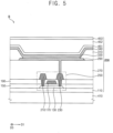
- FIG. 5 is an enlarged cross-sectional view showing region B of the display device of FIG. 3 .
- the display panel 200 may include a substrate 110, a semiconductor element 250, a planarization layer 270, a lower electrode 290, a pixel defining layer 310, a light emitting layer 330, an upper electrode 340, a first thin film encapsulation layer 451, a second thin film encapsulation layer 452, a third thin film encapsulation layer 453, and the like.
- the semiconductor element 250 may include an active layer 130, a gate insulating layer 150, a gate electrode 170, an interlayer insulating layer 190, a source electrode 210, and a drain electrode 230.
- the substrate 110 may include a transparent or opaque material.
- the substrate 110 may be disposed on a lower protective film.
- the substrate 110 may be formed of a transparent resin substrate, such as a polyimide substrate.
- the polyimide substrate may include a first polyimide layer, a barrier film layer, a second polyimide layer, and the like.
- the substrate 110 may include a quartz substrate, a synthetic quartz substrate, a calcium fluoride substrate, a fluorine-doped quartz substrate (F-doped quartz substrate), a soda lime glass substrate, a non-alkali glass substrate, etc.
- a buffer layer may be disposed on the substrate 110.
- the buffer layer may prevent metal atoms or impurities from diffusing from the substrate 110 to the semiconductor element 250, and may control a heat transfer rate during a crystallization process for forming the active layer 130 to obtain a substantially uniform active layer 130.
- the buffer layer may improve flatness of the surface of the substrate 110.
- at least two buffer layers may be provided on the substrate 110, or the buffer layer may be omitted.
- the buffer layer may include an organic material or an inorganic material.
- the active layer 130 may be disposed on the substrate 110.
- the active layer 130 may include a metal oxide semiconductor, an inorganic semiconductor (e.g., amorphous silicon or poly silicon semiconductor), an organic semiconductor, etc.
- the active layer 130 may have source and drain regions.
- the gate insulating layer 150 may be disposed on the active layer 130.
- the gate insulating layer 150 may sufficiently cover the active layer 130 on the substrate 110, and may have a substantially flat top surface without creating a step around the active layer 130.
- the gate insulating layer 150 may be disposed along a profile of the active layer 130 with a substantially uniform thickness to cover the active layer 130 on the substrate 110.
- the gate insulating layer 150 may include a silicon compound, metal oxide, etc.
- the gate insulating layer 150 may include silicon oxide (SiO x ), silicon nitride (SiN x ), silicon oxynitride (SiO x N y ), silicon oxycarbide (SiO x C y ), silicon carbonitride (SiC x N y ), aluminum oxide (AlO x ), aluminum nitride (AlN x ), tantalum oxide (TaO x ), hafnium oxide (HfO x ), zirconium oxide (ZrO x ), titanium oxide (TiO x ), etc.
- the gate insulating layer 150 may have a multilayer structure including a plurality of insulating layers.
- the insulating layers may have different thicknesses and/or may include different materials.
- the gate electrode 170 may be disposed on the gate insulating layer 150.
- the gate electrode 170 may be disposed at a portion of the gate insulating layer 150, under which the active layer 130 is located.
- the gate electrode 170 may include metal, an alloy, metal nitride, conductive metal oxide, a transparent conductive material, etc.
- the gate electrode 170 may include gold (Au), silver (Ag), aluminum (Al), tungsten (W), copper (Cu), platinum (Pt), nickel (Ni), titanium (Ti), palladium (Pd), magnesium (Mg), calcium (Ca), lithium (Li), chromium (Cr), tantalum (Ta), molybdenum (Mo), scandium (Sc), neodymium (Nd), iridium (Ir), an aluminum-containing alloy, aluminum nitride (AlN x ), a silver-containing alloy, tungsten nitride (WN x ), a copper-containing alloy, a molybdenum-containing alloy, titanium nitride (TiN x ), chromium nitride (CrN x ), tantalum nitride (TaN x ), strontium ruthenium oxide (SrRu x O y ), zinc oxide (ZnO x ),
- the interlayer insulating layer 190 may be disposed on the gate electrode 170.
- the interlayer insulating layer 190 may sufficiently cover the gate electrode 170 on the gate insulating layer 150, and may have a substantially flat top surface without creating a step around the gate electrode 170.
- the interlayer insulating layer 190 may be disposed along a profile of the gate electrode 170 with a substantially uniform thickness to cover the gate electrode 170 on the gate insulating layer 150.
- the interlayer insulating layer 190 may include a silicon compound, metal oxide, etc.
- the interlayer insulating layer 190 may have a multilayer structure including a plurality of insulating layers.
- the insulating layers may have different thicknesses and/or may include different materials.
- the source electrode 210 and the drain electrode 230 may be disposed on the interlayer insulating layer 190.
- the source electrode 210 may be connected to the source region of the active layer 130 through a contact hole formed by removing first parts of the gate insulating layer 150 and the interlayer insulating layer 190
- the drain electrode 230 may be connected to the drain region of the active layer 130 through a contact hole formed by removing second parts of the gate insulating layer 150 and the interlayer insulating layer 190.
- Each of the source electrode 210 and the drain electrode 230 may include metal, an alloy, metal nitride, conductive metal oxide, a transparent conductive material, etc. These may be used alone or in combination with each other.
- each of the source electrode 210 and the drain electrode 230 may have a multilayer structure including a plurality of metal layers.
- the metal layers may have different thicknesses and/or may include different materials.
- the semiconductor element 250 including the active layer 130, the gate insulating layer 150, the gate electrode 170, the interlayer insulating layer 190, the source electrode 210, and the drain electrode 230 may be provided.
- the semiconductor element 250 has been described as having a top gate structure, the inventive concept are not limited thereto.
- the semiconductor element 250 may have a bottom gate structure, a double gate structure, etc.
- the display device 100 has been described as including one semiconductor element, the inventive concepts are not limited thereto.
- the display device 100 may include at least one semiconductor element and at least one storage capacitor.
- the planarization layer 270 may be disposed on the interlayer insulating layer 190, the source electrode 210, and the drain electrode 230.
- the planarization layer 270 may have a relatively thick thickness.
- the planarization layer 270 may have a substantially flat top surface.
- a planarization process may be additionally performed on the planarization layer 270.
- the planarization layer 270 may be disposed along a profile of the source electrode 210 and the drain electrode 230 with a substantially uniform thickness on the interlayer insulating layer 190.
- the planarization layer 270 may be formed of an organic material or an inorganic material.
- the planarization layer 270 may include an organic material.
- the planarization layer 270 may include a photoresist, a polyacryl-based resin, a polyimide-based resin, a polyamide-based resin, a siloxane-based resin, an acryl-based resin, an epoxy-based resin, etc.
- the lower electrode 290 may be disposed on the planarization layer 270.
- the lower electrode 290 may be connected to the drain electrode 230 through a contact hole formed by removing a portion of the planarization layer 270, such that the lower electrode 290 may be electrically connected to the semiconductor element 250.
- the lower electrode 290 may include metal, an alloy, metal nitride, conductive metal oxide, a transparent conductive material, etc. These may be used alone or in combination with each other.
- the lower electrode 290 may have a multilayer structure including a plurality of metal layers.
- the metal layers may have different thicknesses and/or may include different materials.
- the pixel defining layer 310 may be disposed on the planarization layer 270.
- the pixel defining layer 310 may expose a portion of a top surface of the lower electrode 290 while covering both sides of the lower electrode 290.
- the pixel defining layer 310 may be formed of an organic material or an inorganic material. In the illustrated exemplary embodiment, the pixel defining layer 310 may include an organic material.
- the light emitting layer 330 may be disposed on the pixel defining layer 310 and the lower electrode 290.
- the light emitting layer 330 may be formed by using at least one of light emitting materials for emitting different colors of light (e.g., red light, green light, blue light, etc.) according to sub-pixels.
- the light emitting layer 330 may be formed by laminating a plurality of light emitting materials for emitting different colors of light, such as red light, green light, and blue light to emit white light as a whole.
- a color filter may be disposed on the light emitting layer 330 that is disposed on the lower electrode 290.
- the color filter may include at least one of a red color filter, a green color filter, and a blue color filter.
- the color filter may include a yellow color filter, a cyan color filter, and a magenta color filter, for example.
- the color filter may include a photosensitive resin or a color photoresist.
- the upper electrode 340 may be disposed on the light emitting layer 330 and the pixel defining layer 310.
- the upper electrode 340 may include metal, an alloy, metal nitride, conductive metal oxide, a transparent conductive material, etc. These may be used alone or in combination with each other.
- the upper electrode 340 may have a multilayer structure including a plurality of metal layers.
- the metal layers may have different thicknesses and/or may include different materials.
- the first thin film encapsulation layer 451 may be disposed on the upper electrode 340.
- the first thin film encapsulation layer 451 may be disposed along a profile of the upper electrode 340 with a substantially uniform thickness to cover the upper electrode 340.
- the first thin film encapsulation layer 451 may prevent the light emitting layer 330 from being deteriorated due to penetration of moisture, oxygen, or the like.
- the first thin film encapsulation layer 451 may also protect the display panel 200 from an external impact.
- the first thin film encapsulation layer 451 may include inorganic materials having flexibility.
- the second thin film encapsulation layer 452 may be disposed on the first thin film encapsulation layer 451.
- the second thin film encapsulation layer 452 may improve flatness of the display panel 200 and protect the display panel 200.
- the second thin film encapsulation layer 452 may include organic materials having flexibility.
- the third thin film encapsulation layer 453 may be disposed on the second thin film encapsulation layer 452.
- the third thin film encapsulation layer 453 may be disposed along a profile of the second thin film encapsulation layer 452 with a substantially uniform thickness to cover the second thin film encapsulation layer 452.
- the third thin film encapsulation layer 453 may prevent the light emitting layer 330 from being deteriorated due to the penetration of moisture, oxygen, or the like together with the first thin film encapsulation layer 451.
- the third thin film encapsulation layer 453 may also protect the display panel 200 from an external impact together with the first thin film encapsulation layer 451 and the second thin film encapsulation layer 452.
- the third thin film encapsulation layer 453 may include inorganic materials having flexibility.
- the display panel 200 including the substrate 110, the semiconductor element 250, the planarization layer 270, the lower electrode 290, the pixel defining layer 310, the light emitting layer 330, the upper electrode 340, the first thin film encapsulation layer 451, the second thin film encapsulation layer 452, and the third thin film encapsulation layer 453 may be provided.
- the display device 100 may include a liquid crystal display device (LCD), a field emission display device (FED), a plasma display device (PDP), or an electrophoretic image display device (EPD).
- LCD liquid crystal display device
- FED field emission display device
- PDP plasma display device
- EPD electrophoretic image display device
- FIG. 6 is a cross-sectional view of a display device according to an embodiment.
- a display device 700 illustrated in FIG. 6 may have a configuration substantially identical or similar to the configuration of the display device 100 described with reference to FIGS. 1 to 5 , except for a first adhesive member 425, a second adhesive member 415, a third adhesive member 205, a fourth adhesive member 436, a fifth adhesive member 437, and a metal member 705.
- FIG. 6 shows a state in which the display device 700 is unfolded.
- the display device 700 may include a display panel 200, a third adhesive member 205, a shock absorbing member 410, a second adhesive member 415, a support member 500, a first adhesive member 425, an elastic member 430, a fourth adhesive member 436, a fifth adhesive member 437, a metal member 705, and a step difference compensation member 460.
- the display device 700 may include a display area 10 and a foldable area 20.
- the display area 10 is an area where an image is displayed from the display panel 200
- the foldable area 20 is an area where the display device 700 is folded or unfolded. A portion of the display area 10 may be defined as the foldable area 20.
- the step difference compensation member 460 may include a first step difference compensation member 461 and a second step difference compensation member 462, and the metal member 705 may include a first metal member 710 and a second metal member 720. Furthermore, a plurality of openings 535, a plurality of protrusions 530, and a plurality of trenches 520 may be formed in the support member 500.
- the first adhesive member 425 may be disposed between the support member 500 and the elastic member 430. In the illustrated embodiment, a top surface of the first adhesive member 425 may make direct contact with the support member 500, and a bottom surface of the first adhesive member 425 may make direct contact with the elastic member 430. In addition, the first adhesive member 425 may cover the openings 535. The first adhesive member 425 may attach the elastic member 430 onto the bottom surface of the support member 500. In the illustrated embodiment, the first adhesive member 425 may not be disposed inside each of the openings 535, such that the openings 535 may be configured as empty spaces.
- the first adhesive member 425 may prevent foreign substances from penetrating into the openings 535 and the trench 520 together with the elastic member 430.
- the first adhesive member 425 may be extended and contracted to prevent the openings 535 from being exposed.
- the first adhesive member 425 may include an optical clear adhesive (OCA), a pressure sensitive adhesive (PSA), a photocurable resin, a thermosetting resin, etc.
- OCA optical clear adhesive
- PSA pressure sensitive adhesive
- the adhesive may include PET, PEN, PP, PC, PS, PSul, PE, PPA, PES, PAR, PCO, MPPO, and the like
- the resin may include an epoxy resin, an amino resin, a phenol resin, a urea resin, a melamine resin, an unsaturated polyester resin, a polyurethane resin, a polyimide resin, and the like.
- the second adhesive member 415 may be disposed between the shock absorbing member 410 and the support member 500.
- a top surface of the second adhesive member 415 may make direct contact with the shock absorbing member 410
- a bottom surface of the second adhesive member 415 may make direct contact with the support member 500.
- the second adhesive member 415 may cover the openings 535.
- the second adhesive member 415 may adhere the shock absorbing member 410 onto a top surface of the support member 500.
- the second adhesive member 415 may not be disposed inside each of the openings 535 such that the openings 535 may be configured as empty spaces.
- the second adhesive member 415 may include an OCA, a PSA, a photocurable resin, a thermosetting resin, etc.
- the third adhesive member 205 may be disposed between the display panel 200 and the shock absorbing member 410.
- a top surface of the third adhesive member 205 may make direct contact with the display panel 200, and a bottom surface of the third adhesive member 205 may make direct contact with the shock absorbing member 410.
- the third adhesive member 205 may adhere the display panel 200 to the shock absorbing member 410.
- the third adhesive member 205 may include an OCA, a PSA, a photocurable resin, a thermosetting resin, etc.
- the metal member 705 may be disposed on the bottom surface of the elastic member 430.
- the first metal member 710 may be disposed at a first portion on the bottom surface of the elastic member 430
- the second metal member 720 may be disposed at a second portion of the bottom surface of the elastic member 430.
- each of the first and second portions of the elastic member 430 may partially overlap the foldable area 20.
- the first metal member 710 and the second metal member 720 may be spaced apart from each other in the first direction D1. A spaced distance may be determined according to the radius of curvature of the foldable area 20.
- the metal member 705 may prevent the display panel 200 from sagging in the foldable area 20, and may serve to block static electricity, electromagnetic waves, electric fields, magnetic fields, and the like which are generated from an outside.
- the metal member 705 may include SUS.
- the metal member may include Au, Ag, Al, W, Cu, Pt, Ni, Ti, Pd, Mg, Ca, Li, Cr, Ta, Mo, Sc, Nd, Ir, an aluminum-containing alloy, AlN x , a silver-containing alloy, WN x , a copper-containing alloy, a molybdenum-containing alloy, TiN x , CrN x , TaN x , SrRu x O y , ZnO x , ITO, SnO x , InO x , GaO x , IZO, etc.
- a step difference compensation member and an adhesive member may be additionally disposed on a bottom surface of the metal member 705.
- the adhesive member may make contact with a set member surrounding the display device 700, and the step difference compensation member may prevent the display panel 200 from sagging in the foldable area 20 together with the metal member 705.
- the fourth adhesive member 436 may be disposed between the first metal member 710 and the elastic member 430. In the embodiments, a top surface of the fourth adhesive member 436 may make direct contact with the elastic member 430, and a bottom surface of the fourth adhesive member 436 may make direct contact with the first metal member 710. The fourth adhesive member 436 may adhere the first metal member 710 to the first portion on the bottom surface of the elastic member 430.
- the fifth adhesive member 437 may be disposed between the second metal member 720 and the elastic member 430. In the exemplary embodiments, a top surface of the fifth adhesive member 437 may make direct contact with the elastic member 430, and a bottom surface of the fifth adhesive member 437 may make direct contact with the second metal member 720.
- the fourth adhesive member 436 and the fifth adhesive member 437 may be spaced apart from each other in the first direction D1.
- the fifth adhesive member 437 may adhere the second metal member 720 to the second portion on the bottom surface of the elastic member 430.
- Each of the fourth adhesive member 436 and the fifth adhesive member 437 may include an OCA, a PSA, a photocurable resin, a thermosetting resin, etc.
- a first step difference compensation member may be additionally disposed at the first portion on the bottom surface of the elastic member 430 together with the fourth adhesive member 436, and a second step difference compensation member may be additionally disposed at the second portion on the bottom surface of the elastic member 430 together with the fifth adhesive member 437.
- the first and second step difference compensation members may prevent the display panel 200 from sagging in the foldable area 20.
- the step difference compensation member 460 may be spaced apart from the first adhesive member 425, the elastic member 430, the fourth adhesive member 436, and the metal member 705 on the bottom surface of the support member 500.
- the first step difference compensation member 461 may be disposed at the first portion on the bottom surface of the support member 500
- the second step difference compensation member 462 may be disposed at the second portion on the bottom surface of the support member 500.
- the bottom surface of the step difference compensation member 460 may be located at the same level as the bottom surface of the metal member 705.
- the step difference compensation member 460 may prevent the display panel 200 from sagging in a portion where the metal member 705 is not disposed.
- the step difference compensation member 460 may include PET, PEN, PP, PC, PS, PSul, PE, PPA, PES, PAR, PCO, MPPO, etc.
- an additional adhesive member may be disposed on the bottom surface of the step difference compensation member 460 to make contact with a set member surrounding the display device 700.
- the display device 700 includes the elastic member 430 disposed on the openings 535 to prevent the openings 535 from being exposed, so that the foreign substances may not be located in the openings 535. In this manner, defects may not occur in the foldable area 20 of the display device 700.
- the display device 700 includes the metal member 705, so that the display panel 200 may be prevented from sagging in the foldable area 20, and static electricity, electromagnetic waves, electric fields, magnetic fields, and the like, which may be generated from the outside, may be blocked.
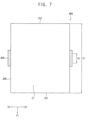
- FIG. 7 is a plan view of a display device according to an embodiment
- FIG. 8 is a plan view showing a rear side of the display device of FIG. 7
- FIG. 9 is a side view showing a lateral side of the display device of FIG. 7
- a display device 800 illustrated in FIGS. 7 , 8 , and 9 may have a configuration substantially identical or similar to the configuration of the display device 100 described with reference to FIGS. 1 to 5 , except for an elastic member 830. As such, repeated descriptions of components substantially identical or similar to the components described with reference to FIGS. 1 to 5 will be omitted to avoid redundancy.
- FIGS. 7 , 8 , and 9 show a state in which the display device 800 is unfolded.
- the display device 800 may include a display panel 200, a shock absorbing member 410, a support member 500, an elastic member 830, and a step difference compensation member 460.
- the display device 800 may include a display area 10 and a foldable area 20.
- the display area 10 is an area where an image is displayed from the display panel 200
- the foldable area 20 is an area where the display device 800 is folded or unfolded.
- a portion of the display area 10 may be defined as the foldable area 20.
- the step difference compensation member 460 may include a first step difference compensation member 461 and a second step difference compensation member 462.
- a plurality of openings 535, a plurality of protrusions 530, and a plurality of trenches 520 may be formed in the support member 500.
- the elastic member 830 may be disposed at a portion of the bottom surface of the support member 500 and a portion of a side surface of the support member 500. In particular, the elastic member 830 may overlap the trenches 520 in the foldable area 20 on the side surface of the support member 500, while overlapping the openings 535 in the foldable area 20 on the bottom surface of the support member 500. In this manner, the elastic member 830 may prevent the openings 535 and the trenches 520 from being exposed. In the illustrated embodiment, the elastic member 830 may not be disposed inside each of the openings 535 and the trenches 520, such that the openings 535 and the trenches 520 may be configured as empty spaces.
- the elastic member 830 may prevent foreign substances from penetrating into the openings 535 and the trenches 520. In addition, while the display device 800 is repeatedly folded and unfolded, the elastic member 830 may be extended and contracted to prevent the openings 535 and the trenches 520 from being exposed.
- the elastic member 830 may include an elastomer having a relatively large elastic force or a relatively large restoring force.
- the elastic member 830 may include an elastic material, such as silicone, urethane, or TPU.
- the display device 800 includes the elastic member 830, so that the openings 535 and the trenches 520 of the support member 500 may be covered to prevent the foreign substances from being located in the openings 535 and the trenches 520. Accordingly, defects due to the foreign substances may not occur in the display device 800.
- inventive concepts may be applied to various electronic devices including a display device.
- the inventive concepts may be applied to a vehicle-display device, a ship-display device, an aircraft-display device, portable communication devices, display devices for display or for information transfer, a medical-display device, etc.
- the display device includes the elastic member disposed on the openings to prevent the openings from being exposed, the foreign substances may not be located in the openings. Accordingly, defects may not occur in the foldable area of the display device.
- the display panel may be prevented from sagging in the foldable area, and static electricity, electromagnetic waves, electric fields, magnetic fields, and the like, which may be generated from the outside, may be blocked.
Landscapes
- Engineering & Computer Science (AREA)
- Physics & Mathematics (AREA)
- Theoretical Computer Science (AREA)
- General Physics & Mathematics (AREA)
- Computer Hardware Design (AREA)
- Nonlinear Science (AREA)
- Human Computer Interaction (AREA)
- General Engineering & Computer Science (AREA)
- Chemical & Material Sciences (AREA)
- Crystallography & Structural Chemistry (AREA)
- Mathematical Physics (AREA)
- Optics & Photonics (AREA)
- Electroluminescent Light Sources (AREA)
- Devices For Indicating Variable Information By Combining Individual Elements (AREA)
- Microelectronics & Electronic Packaging (AREA)
- Liquid Crystal (AREA)
Claims (18)
- Anzeigevorrichtung (100), umfassend:ein Anzeigefeld (200), das einen faltbaren Bereich (20) aufweist;ein Stützelement (500), das auf einer unteren Fläche des Anzeigefelds (200) angeordnet ist und eine Vielzahl von Öffnungen (535) beinhaltet, die in dem faltbaren Bereich (20) gebildet ist; undein elastisches Element (430), das auf einer unteren Fläche des Stützelements (500) angeordnet ist und die Öffnungen (535) in dem faltbaren Bereich (20) überlappt,dadurch gekennzeichnet, dassdie Anzeigevorrichtung (100) ferner Folgendes umfasst:ein erstes Metallelement (710), das an einem ersten Abschnitt auf einer unteren Fläche des elastischen Elements (430) angeordnet ist; undein zweites Metallelement (720), das an einem zweiten Abschnitt auf der unteren Fläche des elastischen Elements (430) angeordnet ist, während es von dem ersten Metallelement (710) beabstandet ist,wobei jeder von dem ersten und dem zweiten Abschnitt den faltbaren Bereich (20) teilweise überlappt.
- Anzeigevorrichtung (100) nach Anspruch 1, wobei:das Anzeigefeld (200) ferner einen Anzeigebereich (10) beinhaltet; undein Abschnitt des Anzeigebereichs (10) als der faltbare Bereich (20) definiert ist.
- Anzeigevorrichtung (100) nach mindestens einem der Ansprüche 1 oder 2, wobei:die Öffnungen (535) des Stützelements (500) eine erste bis eine n-te Öffnung beinhalten, die in einer ersten Richtung (D1) parallel zu einer oberen Fläche des Anzeigefelds (200) angeordnet sind, wobei n eine ganze Zahl von 1 oder mehr ist; undeine k-te Öffnung an einer Position angeordnet ist, die in eine zweite Richtung (D2) senkrecht zu der ersten Richtung (D1) verschoben ist, wobei k eine gerade Zahl zwischen 1 und n ist.
- Anzeigevorrichtung (100) nach Anspruch 3, wobei das Stützelement (500) ferner Vorsprünge beinhaltet, die in einer dritten Richtung (D3) gegenüber der zweiten Richtung (D2) in Bezug auf jede der (k-1)-ten und der (k+1)-ten Öffnungen unter der ersten bis n-ten Öffnung angeordnet sind.
- Anzeigevorrichtung (100) nach Anspruch 4, wobei:ein Raum zwischen zwei benachbarten Vorsprüngen (530) als eine Rinne (520) definiert ist; undsich das elastische Element (430) zu einer Seitenfläche des Stützelements (500) erstreckt, um die Rinne (520) abzudecken.
- Anzeigevorrichtung (100) nach mindestens einem der Ansprüche 1 bis 5, ferner umfassend:ein erstes Stufendifferenzausgleichselement (461), das an einem ersten Abschnitt auf der unteren Fläche des Stützelements (500) angeordnet ist; undein zweites Stufendifferenzausgleichselement (462), das an einem zweiten Abschnitt auf der unteren Fläche des Stützelements (500) angeordnet ist.
- Anzeigevorrichtung (100) nach Anspruch 6, wobei eine untere Fläche von jedem von dem ersten (461) und dem zweiten Stufendifferenzausgleichselement (462) auf einer gleichen Ebene wie eine untere Fläche des elastischen Elements (430) angeordnet ist.
- Anzeigevorrichtung (100) nach mindestens einem der Ansprüche 1 bis 7, ferner umfassend ein erstes Klebeelement (425), das zwischen dem Stützelement (500) und dem elastischen Element (430) angeordnet ist.
- Anzeigevorrichtung (700) nach Anspruch 8, wobei das erste Klebeelement (425) das Stützelement (500) und das elastische Element (430) berührt, um die Öffnungen (535) abzudecken.
- Anzeigevorrichtung (100) nach mindestens einem der Ansprüche 1 bis 9, ferner umfassend ein Stoßdämpfungselement (410), das zwischen dem Stützelement (500) und dem Anzeigefeld (200) angeordnet ist.
- Anzeigevorrichtung (100) nach Anspruch 10, ferner umfassend:ein zweites Klebeelement (415), das zwischen dem Stoßdämpfungselement (410) und dem Stützelement (500) angeordnet ist; undein drittes Klebeelement (205), das zwischen dem Anzeigefeld (200) und dem Stoßdämpfungselement (410) angeordnet ist.
- Anzeigevorrichtung (100) nach Anspruch 11, wobei das zweite Klebeelement (415) das Stoßdämpfungselement (410) und das Stützelement (500) berührt, um die Öffnungen (535) abzudecken.
- Anzeigevorrichtung (100) nach Anspruch 11, wobei das dritte Klebeelement (205) das Anzeigefeld (200) und das Stoßdämpfungselement (410) berührt.
- Anzeigevorrichtung (100) nach Anspruch 1, ferner umfassend:ein viertes Klebeelement (436), das zwischen dem ersten Metallelement (710) und dem elastischen Element (430) angeordnet ist; undein fünftes Klebeelement (437), das zwischen dem zweiten Metallelement (720) und dem elastischen Element (430) angeordnet ist, während es von dem vierten Klebeelement (436) beabstandet ist.
- Anzeigevorrichtung (100) nach mindestens einem der Ansprüche 1 bis 14, ferner umfassend:ein erstes Stufendifferenzausgleichselement (461), das an dem ersten Abschnitt auf der unteren Fläche des Stützelements (500) angeordnet ist; undein zweites Stufendifferenzausgleichselement (462), das an dem zweiten Abschnitt auf der unteren Fläche des Stützelements (500) angeordnet ist.
- Anzeigevorrichtung (100) nach Anspruch 15, wobei eine untere Fläche von jedem von dem ersten und dem zweiten Stufendifferenzausgleichselement (461, 462) auf einer gleichen Ebene wie eine untere Fläche von jedem von dem ersten (710) und dem zweiten Metallelement (720) angeordnet ist.
- Anzeigevorrichtung (100) nach mindestens einem der Ansprüche 1 bis 16, wobei das elastische Element (430) dazu konfiguriert ist, sich zu erstrecken, um die Öffnungen (535) des Stützelements (500) zu bedecken, das in dem faltbaren Bereich (20) angeordnet ist, wenn das Anzeigefeld (200) gefaltet ist.
- Anzeigevorrichtung (100) nach mindestens einem der Ansprüche 1 bis 17, wobei die Öffnung (535) einen leeren Raum umfasst.
Priority Applications (1)
| Application Number | Priority Date | Filing Date | Title |
|---|---|---|---|
| EP24218938.9A EP4513296B1 (de) | 2019-06-25 | 2020-06-22 | Elektronische vorrichtung |
Applications Claiming Priority (1)
| Application Number | Priority Date | Filing Date | Title |
|---|---|---|---|
| KR1020190075942A KR102671010B1 (ko) | 2019-06-25 | 2019-06-25 | 표시 장치 |
Related Child Applications (1)
| Application Number | Title | Priority Date | Filing Date |
|---|---|---|---|
| EP24218938.9A Division EP4513296B1 (de) | 2019-06-25 | 2020-06-22 | Elektronische vorrichtung |
Publications (2)
| Publication Number | Publication Date |
|---|---|
| EP3757668A1 EP3757668A1 (de) | 2020-12-30 |
| EP3757668B1 true EP3757668B1 (de) | 2025-01-01 |
Family
ID=71120111
Family Applications (2)
| Application Number | Title | Priority Date | Filing Date |
|---|---|---|---|
| EP20181422.5A Active EP3757668B1 (de) | 2019-06-25 | 2020-06-22 | Anzeigevorrichtung |
| EP24218938.9A Active EP4513296B1 (de) | 2019-06-25 | 2020-06-22 | Elektronische vorrichtung |
Family Applications After (1)
| Application Number | Title | Priority Date | Filing Date |
|---|---|---|---|
| EP24218938.9A Active EP4513296B1 (de) | 2019-06-25 | 2020-06-22 | Elektronische vorrichtung |
Country Status (4)
| Country | Link |
|---|---|
| US (3) | US11296286B2 (de) |
| EP (2) | EP3757668B1 (de) |
| KR (1) | KR102671010B1 (de) |
| CN (1) | CN112133196A (de) |
Families Citing this family (17)
| Publication number | Priority date | Publication date | Assignee | Title |
|---|---|---|---|---|
| KR102724814B1 (ko) | 2019-08-27 | 2024-11-04 | 삼성디스플레이 주식회사 | 표시 장치 |
| WO2020202359A1 (ja) * | 2019-03-29 | 2020-10-08 | シャープ株式会社 | フォルダブルディスプレイ |
| CN110581156A (zh) * | 2019-08-29 | 2019-12-17 | 武汉华星光电半导体显示技术有限公司 | 柔性有机发光二极管显示面板及可弯折的显示装置 |
| KR102727809B1 (ko) * | 2019-12-10 | 2024-11-07 | 엘지디스플레이 주식회사 | 폴더블 표시장치 |
| US11503727B2 (en) | 2020-02-14 | 2022-11-15 | Samsung Display Co., Ltd. | Display device |
| KR20210157387A (ko) * | 2020-06-15 | 2021-12-28 | 우한 차이나 스타 옵토일렉트로닉스 세미컨덕터 디스플레이 테크놀로지 컴퍼니 리미티드 | 디스플레이 패널 및 디스플레이 장치 |
| US12295110B2 (en) * | 2020-09-30 | 2025-05-06 | Sharp Kabushiki Kaisha | Foldable display and method for manufacturing foldable display |
| KR20220065145A (ko) * | 2020-11-12 | 2022-05-20 | 삼성디스플레이 주식회사 | 표시장치 |
| KR102953683B1 (ko) * | 2020-12-02 | 2026-04-17 | 삼성디스플레이 주식회사 | 표시장치 |
| KR102846108B1 (ko) * | 2020-12-30 | 2025-08-12 | 엘지디스플레이 주식회사 | 폴더블 표시 장치 |
| KR102923423B1 (ko) * | 2021-01-27 | 2026-02-05 | 삼성디스플레이 주식회사 | 표시 장치 |
| CN215068979U (zh) * | 2021-03-26 | 2021-12-07 | 京东方科技集团股份有限公司 | 柔性支撑层、柔性显示模组以及柔性显示装置 |
| KR20220147772A (ko) * | 2021-04-27 | 2022-11-04 | 삼성디스플레이 주식회사 | 표시 장치 |
| KR20220167845A (ko) | 2021-06-14 | 2022-12-22 | 삼성디스플레이 주식회사 | 표시 장치 및 이를 포함하는 전자 장치 |
| KR102868426B1 (ko) * | 2021-06-24 | 2025-10-02 | 엘지디스플레이 주식회사 | 쿠션 플레이트 및 이를 포함하는 표시 장치 |
| KR20230020071A (ko) | 2021-08-02 | 2023-02-10 | 삼성디스플레이 주식회사 | 표시장치 및 이를 포함하는 전자장치 |
| KR20230121205A (ko) * | 2022-02-09 | 2023-08-18 | 삼성디스플레이 주식회사 | 표시 장치 |
Family Cites Families (37)
| Publication number | Priority date | Publication date | Assignee | Title |
|---|---|---|---|---|
| CN103460823B (zh) | 2011-04-13 | 2016-08-17 | 株式会社村田制作所 | 柔性多层基板 |
| KR20130118483A (ko) * | 2012-04-20 | 2013-10-30 | 강호림 | 표시 소자 보호용 충격 흡수 필름 |
| KR20150017819A (ko) * | 2013-08-07 | 2015-02-23 | 삼성디스플레이 주식회사 | 윈도우 부재 및 이를 포함하는 표시장치 |
| KR101663728B1 (ko) * | 2013-08-26 | 2016-10-07 | 삼성전자주식회사 | 플렉서블 디스플레이 소자를 구비한 접철식 전자 기기 |
| KR102405257B1 (ko) * | 2015-01-28 | 2022-06-03 | 삼성디스플레이 주식회사 | 표시 장치 |
| KR102414855B1 (ko) | 2015-04-30 | 2022-07-01 | 삼성전자주식회사 | 플렉시블 전자 장치 |
| KR102506631B1 (ko) * | 2015-06-08 | 2023-03-07 | 엘지디스플레이 주식회사 | 폴더블 표시장치 |
| KR20170064453A (ko) | 2015-11-30 | 2017-06-09 | 엘지디스플레이 주식회사 | 폴더블 표시장치 |
| KR102535208B1 (ko) * | 2016-03-10 | 2023-05-22 | 삼성디스플레이 주식회사 | 표시 장치 |
| KR102550696B1 (ko) * | 2016-04-08 | 2023-07-04 | 삼성디스플레이 주식회사 | 디스플레이 장치 |
| CN109792462B (zh) * | 2016-09-28 | 2021-01-29 | 夏普株式会社 | 信息处理装置 |
| KR102578589B1 (ko) * | 2016-09-30 | 2023-09-14 | 엘지디스플레이 주식회사 | 플렉서블 표시장치 |
| KR102631257B1 (ko) * | 2016-11-18 | 2024-01-31 | 삼성디스플레이 주식회사 | 디스플레이 장치 |
| KR102672832B1 (ko) * | 2016-12-30 | 2024-06-05 | 엘지디스플레이 주식회사 | 폴더블 표시 장치 |
| KR20180111281A (ko) * | 2017-03-31 | 2018-10-11 | 엘지디스플레이 주식회사 | 플렉서블 표시장치 |
| CN108665804A (zh) | 2017-03-31 | 2018-10-16 | 元太科技工业股份有限公司 | 可折式电子纸显示设备及其制造方法 |
| KR102379216B1 (ko) * | 2017-04-24 | 2022-03-28 | 삼성디스플레이 주식회사 | 표시 장치 |
| KR102265542B1 (ko) * | 2017-05-31 | 2021-06-15 | 엘지디스플레이 주식회사 | 플렉서블 표시 장치 |
| KR101834793B1 (ko) | 2017-07-28 | 2018-03-06 | 엘지디스플레이 주식회사 | 플렉서블 디스플레이 및 이를 포함하는 전자 장치 |
| KR101888451B1 (ko) * | 2017-08-31 | 2018-08-16 | 엘지디스플레이 주식회사 | 접착제 및 이를 적용한 플렉서블 디스플레이 |
| CN107437378B (zh) | 2017-09-20 | 2020-09-11 | 上海天马微电子有限公司 | 柔性显示模组 |
| CN109727538A (zh) * | 2017-10-31 | 2019-05-07 | 乐金显示有限公司 | 可卷曲显示器 |
| KR102636685B1 (ko) | 2017-10-31 | 2024-02-15 | 엘지디스플레이 주식회사 | 롤러블 디스플레이 |
| KR102590012B1 (ko) * | 2017-11-30 | 2023-10-16 | 엘지디스플레이 주식회사 | 접착제 및 이를 적용한 플렉서블 디스플레이 |
| KR102422072B1 (ko) * | 2017-12-04 | 2022-07-18 | 엘지디스플레이 주식회사 | 폴더블 디스플레이 장치 |
| CN108155218A (zh) * | 2017-12-29 | 2018-06-12 | 云谷(固安)科技有限公司 | 柔性显示屏 |
| CN108428731B (zh) * | 2018-05-17 | 2021-01-01 | 武汉华星光电半导体显示技术有限公司 | 柔性oled显示面板及柔性oled显示装置 |
| CN208141720U (zh) * | 2018-05-28 | 2018-11-23 | 京东方科技集团股份有限公司 | 柔性支撑件、柔性显示基板及显示装置 |
| CN108898954B (zh) * | 2018-07-18 | 2024-02-23 | 昆山国显光电有限公司 | 显示面板和显示面板制作方法 |
| CN109036133A (zh) | 2018-07-28 | 2018-12-18 | 蒙凤英 | 背板及显示组件 |
| CN208607861U (zh) * | 2018-08-09 | 2019-03-15 | 京东方科技集团股份有限公司 | 柔性面板模组和显示装置 |
| CN109545087A (zh) | 2018-12-03 | 2019-03-29 | 武汉华星光电半导体显示技术有限公司 | 可折叠背板结构及其显示装置 |
| CN109671753B (zh) * | 2018-12-14 | 2021-06-01 | 武汉华星光电半导体显示技术有限公司 | 显示装置及其制造方法 |
| CN109616018A (zh) * | 2019-01-17 | 2019-04-12 | 云谷(固安)科技有限公司 | 一种折叠柔性显示装置 |
| EP3893093A4 (de) * | 2019-02-01 | 2022-02-16 | Huawei Technologies Co., Ltd. | Trägerblatt für eine faltbare endgerätevorrichtung sowie faltbare endgerätevorrichtung |
| KR102827526B1 (ko) * | 2019-10-22 | 2025-06-30 | 엘지디스플레이 주식회사 | 폴더블 디스플레이 장치 |
| KR102727809B1 (ko) * | 2019-12-10 | 2024-11-07 | 엘지디스플레이 주식회사 | 폴더블 표시장치 |
-
2019
- 2019-06-25 KR KR1020190075942A patent/KR102671010B1/ko active Active
-
2020
- 2020-03-16 US US16/819,366 patent/US11296286B2/en active Active
- 2020-06-22 EP EP20181422.5A patent/EP3757668B1/de active Active
- 2020-06-22 EP EP24218938.9A patent/EP4513296B1/de active Active
- 2020-06-23 CN CN202010578763.XA patent/CN112133196A/zh active Pending
-
2022
- 2022-04-04 US US17/713,159 patent/US12075689B2/en active Active
-
2024
- 2024-07-26 US US18/786,005 patent/US20240389448A1/en active Pending
Also Published As
| Publication number | Publication date |
|---|---|
| US20220231241A1 (en) | 2022-07-21 |
| CN112133196A (zh) | 2020-12-25 |
| US20200411777A1 (en) | 2020-12-31 |
| US11296286B2 (en) | 2022-04-05 |
| EP4513296B1 (de) | 2026-05-20 |
| KR102671010B1 (ko) | 2024-06-03 |
| EP3757668A1 (de) | 2020-12-30 |
| KR20210000809A (ko) | 2021-01-06 |
| US20240389448A1 (en) | 2024-11-21 |
| US12075689B2 (en) | 2024-08-27 |
| EP4513296A3 (de) | 2025-05-07 |
| EP4513296A2 (de) | 2025-02-26 |
Similar Documents
| Publication | Publication Date | Title |
|---|---|---|
| EP3786692B1 (de) | Anzeigevorrichtung | |
| US12075689B2 (en) | Display device having flexible support member having openings | |
| EP3805896B1 (de) | Faltbare anzeigevorrichtung mit flexiblem faltbereich und verfahren zu deren herstellung | |
| CN113112910B (zh) | 有机发光显示装置 | |
| US11501668B2 (en) | Display device | |
| CN112447101B (zh) | 显示装置及显示装置的制造方法 | |
| EP3848775B1 (de) | Anzeigevorrichtung | |
| US12134254B2 (en) | Protective film and display device including the same | |
| CN114823801A (zh) | 显示装置 |
Legal Events
| Date | Code | Title | Description |
|---|---|---|---|
| PUAI | Public reference made under article 153(3) epc to a published international application that has entered the european phase |
Free format text: ORIGINAL CODE: 0009012 |
|
| STAA | Information on the status of an ep patent application or granted ep patent |
Free format text: STATUS: THE APPLICATION HAS BEEN PUBLISHED |
|
| AK | Designated contracting states |
Kind code of ref document: A1 Designated state(s): AL AT BE BG CH CY CZ DE DK EE ES FI FR GB GR HR HU IE IS IT LI LT LU LV MC MK MT NL NO PL PT RO RS SE SI SK SM TR |
|
| AX | Request for extension of the european patent |
Extension state: BA ME |
|
| STAA | Information on the status of an ep patent application or granted ep patent |
Free format text: STATUS: REQUEST FOR EXAMINATION WAS MADE |
|
| 17P | Request for examination filed |
Effective date: 20210630 |
|
| RBV | Designated contracting states (corrected) |
Designated state(s): AL AT BE BG CH CY CZ DE DK EE ES FI FR GB GR HR HU IE IS IT LI LT LU LV MC MK MT NL NO PL PT RO RS SE SI SK SM TR |
|
| STAA | Information on the status of an ep patent application or granted ep patent |
Free format text: STATUS: EXAMINATION IS IN PROGRESS |
|
| 17Q | First examination report despatched |
Effective date: 20221024 |
|
| P01 | Opt-out of the competence of the unified patent court (upc) registered |
Effective date: 20230516 |
|
| GRAP | Despatch of communication of intention to grant a patent |
Free format text: ORIGINAL CODE: EPIDOSNIGR1 |
|
| STAA | Information on the status of an ep patent application or granted ep patent |
Free format text: STATUS: GRANT OF PATENT IS INTENDED |
|
| RIC1 | Information provided on ipc code assigned before grant |
Ipc: G06F 1/16 20060101ALI20240716BHEP Ipc: G02F 1/1333 20060101AFI20240716BHEP |
|
| INTG | Intention to grant announced |
Effective date: 20240726 |
|
| GRAS | Grant fee paid |
Free format text: ORIGINAL CODE: EPIDOSNIGR3 |
|
| GRAA | (expected) grant |
Free format text: ORIGINAL CODE: 0009210 |
|
| STAA | Information on the status of an ep patent application or granted ep patent |
Free format text: STATUS: THE PATENT HAS BEEN GRANTED |
|
| AK | Designated contracting states |
Kind code of ref document: B1 Designated state(s): AL AT BE BG CH CY CZ DE DK EE ES FI FR GB GR HR HU IE IS IT LI LT LU LV MC MK MT NL NO PL PT RO RS SE SI SK SM TR |
|
| REG | Reference to a national code |
Ref country code: GB Ref legal event code: FG4D |
|
| REG | Reference to a national code |
Ref country code: DE Ref legal event code: R096 Ref document number: 602020043937 Country of ref document: DE |
|
| REG | Reference to a national code |
Ref country code: CH Ref legal event code: EP |
|
| REG | Reference to a national code |
Ref country code: IE Ref legal event code: FG4D |
|
| REG | Reference to a national code |
Ref country code: LT Ref legal event code: MG9D |
|
| REG | Reference to a national code |
Ref country code: NL Ref legal event code: MP Effective date: 20250101 |
|
| REG | Reference to a national code |
Ref country code: AT Ref legal event code: MK05 Ref document number: 1756848 Country of ref document: AT Kind code of ref document: T Effective date: 20250101 |
|
| PG25 | Lapsed in a contracting state [announced via postgrant information from national office to epo] |
Ref country code: NL Free format text: LAPSE BECAUSE OF FAILURE TO SUBMIT A TRANSLATION OF THE DESCRIPTION OR TO PAY THE FEE WITHIN THE PRESCRIBED TIME-LIMIT Effective date: 20250101 |
|
| PG25 | Lapsed in a contracting state [announced via postgrant information from national office to epo] |
Ref country code: FI Free format text: LAPSE BECAUSE OF FAILURE TO SUBMIT A TRANSLATION OF THE DESCRIPTION OR TO PAY THE FEE WITHIN THE PRESCRIBED TIME-LIMIT Effective date: 20250101 |
|
| PG25 | Lapsed in a contracting state [announced via postgrant information from national office to epo] |
Ref country code: PL Free format text: LAPSE BECAUSE OF FAILURE TO SUBMIT A TRANSLATION OF THE DESCRIPTION OR TO PAY THE FEE WITHIN THE PRESCRIBED TIME-LIMIT Effective date: 20250101 |
|
| PGFP | Annual fee paid to national office [announced via postgrant information from national office to epo] |
Ref country code: DE Payment date: 20250520 Year of fee payment: 6 |
|
| PG25 | Lapsed in a contracting state [announced via postgrant information from national office to epo] |
Ref country code: ES Free format text: LAPSE BECAUSE OF FAILURE TO SUBMIT A TRANSLATION OF THE DESCRIPTION OR TO PAY THE FEE WITHIN THE PRESCRIBED TIME-LIMIT Effective date: 20250101 |
|
| PGFP | Annual fee paid to national office [announced via postgrant information from national office to epo] |
Ref country code: GB Payment date: 20250520 Year of fee payment: 6 |
|
| PG25 | Lapsed in a contracting state [announced via postgrant information from national office to epo] |
Ref country code: NO Free format text: LAPSE BECAUSE OF FAILURE TO SUBMIT A TRANSLATION OF THE DESCRIPTION OR TO PAY THE FEE WITHIN THE PRESCRIBED TIME-LIMIT Effective date: 20250401 Ref country code: IS Free format text: LAPSE BECAUSE OF FAILURE TO SUBMIT A TRANSLATION OF THE DESCRIPTION OR TO PAY THE FEE WITHIN THE PRESCRIBED TIME-LIMIT Effective date: 20250501 |
|
| PG25 | Lapsed in a contracting state [announced via postgrant information from national office to epo] |
Ref country code: HR Free format text: LAPSE BECAUSE OF FAILURE TO SUBMIT A TRANSLATION OF THE DESCRIPTION OR TO PAY THE FEE WITHIN THE PRESCRIBED TIME-LIMIT Effective date: 20250101 |
|
| PG25 | Lapsed in a contracting state [announced via postgrant information from national office to epo] |
Ref country code: LV Free format text: LAPSE BECAUSE OF FAILURE TO SUBMIT A TRANSLATION OF THE DESCRIPTION OR TO PAY THE FEE WITHIN THE PRESCRIBED TIME-LIMIT Effective date: 20250101 Ref country code: PT Free format text: LAPSE BECAUSE OF FAILURE TO SUBMIT A TRANSLATION OF THE DESCRIPTION OR TO PAY THE FEE WITHIN THE PRESCRIBED TIME-LIMIT Effective date: 20250502 |
|
| PGFP | Annual fee paid to national office [announced via postgrant information from national office to epo] |
Ref country code: FR Payment date: 20250521 Year of fee payment: 6 |
|
| PG25 | Lapsed in a contracting state [announced via postgrant information from national office to epo] |
Ref country code: GR Free format text: LAPSE BECAUSE OF FAILURE TO SUBMIT A TRANSLATION OF THE DESCRIPTION OR TO PAY THE FEE WITHIN THE PRESCRIBED TIME-LIMIT Effective date: 20250402 Ref country code: BG Free format text: LAPSE BECAUSE OF FAILURE TO SUBMIT A TRANSLATION OF THE DESCRIPTION OR TO PAY THE FEE WITHIN THE PRESCRIBED TIME-LIMIT Effective date: 20250101 |
|
| PG25 | Lapsed in a contracting state [announced via postgrant information from national office to epo] |
Ref country code: AT Free format text: LAPSE BECAUSE OF FAILURE TO SUBMIT A TRANSLATION OF THE DESCRIPTION OR TO PAY THE FEE WITHIN THE PRESCRIBED TIME-LIMIT Effective date: 20250101 |
|
| PG25 | Lapsed in a contracting state [announced via postgrant information from national office to epo] |
Ref country code: CZ Free format text: LAPSE BECAUSE OF FAILURE TO SUBMIT A TRANSLATION OF THE DESCRIPTION OR TO PAY THE FEE WITHIN THE PRESCRIBED TIME-LIMIT Effective date: 20250101 |
|
| PG25 | Lapsed in a contracting state [announced via postgrant information from national office to epo] |
Ref country code: SE Free format text: LAPSE BECAUSE OF FAILURE TO SUBMIT A TRANSLATION OF THE DESCRIPTION OR TO PAY THE FEE WITHIN THE PRESCRIBED TIME-LIMIT Effective date: 20250101 |
|
| REG | Reference to a national code |
Ref country code: DE Ref legal event code: R097 Ref document number: 602020043937 Country of ref document: DE |
|
| PG25 | Lapsed in a contracting state [announced via postgrant information from national office to epo] |
Ref country code: SM Free format text: LAPSE BECAUSE OF FAILURE TO SUBMIT A TRANSLATION OF THE DESCRIPTION OR TO PAY THE FEE WITHIN THE PRESCRIBED TIME-LIMIT Effective date: 20250101 |
|
| PG25 | Lapsed in a contracting state [announced via postgrant information from national office to epo] |
Ref country code: DK Free format text: LAPSE BECAUSE OF FAILURE TO SUBMIT A TRANSLATION OF THE DESCRIPTION OR TO PAY THE FEE WITHIN THE PRESCRIBED TIME-LIMIT Effective date: 20250101 |
|
| PG25 | Lapsed in a contracting state [announced via postgrant information from national office to epo] |
Ref country code: IT Free format text: LAPSE BECAUSE OF FAILURE TO SUBMIT A TRANSLATION OF THE DESCRIPTION OR TO PAY THE FEE WITHIN THE PRESCRIBED TIME-LIMIT Effective date: 20250101 |
|
| PG25 | Lapsed in a contracting state [announced via postgrant information from national office to epo] |
Ref country code: EE Free format text: LAPSE BECAUSE OF FAILURE TO SUBMIT A TRANSLATION OF THE DESCRIPTION OR TO PAY THE FEE WITHIN THE PRESCRIBED TIME-LIMIT Effective date: 20250101 |
|
| PG25 | Lapsed in a contracting state [announced via postgrant information from national office to epo] |
Ref country code: RO Free format text: LAPSE BECAUSE OF FAILURE TO SUBMIT A TRANSLATION OF THE DESCRIPTION OR TO PAY THE FEE WITHIN THE PRESCRIBED TIME-LIMIT Effective date: 20250101 |
|
| PG25 | Lapsed in a contracting state [announced via postgrant information from national office to epo] |
Ref country code: SK Free format text: LAPSE BECAUSE OF FAILURE TO SUBMIT A TRANSLATION OF THE DESCRIPTION OR TO PAY THE FEE WITHIN THE PRESCRIBED TIME-LIMIT Effective date: 20250101 |
|
| PLBE | No opposition filed within time limit |
Free format text: ORIGINAL CODE: 0009261 |
|
| STAA | Information on the status of an ep patent application or granted ep patent |
Free format text: STATUS: NO OPPOSITION FILED WITHIN TIME LIMIT |
|
| REG | Reference to a national code |
Ref country code: CH Ref legal event code: L10 Free format text: ST27 STATUS EVENT CODE: U-0-0-L10-L00 (AS PROVIDED BY THE NATIONAL OFFICE) Effective date: 20251112 |
|
| 26N | No opposition filed |
Effective date: 20251002 |
|
| REG | Reference to a national code |
Ref country code: CH Ref legal event code: H13 Free format text: ST27 STATUS EVENT CODE: U-0-0-H10-H13 (AS PROVIDED BY THE NATIONAL OFFICE) Effective date: 20260127 |
|
| PG25 | Lapsed in a contracting state [announced via postgrant information from national office to epo] |
Ref country code: MC Free format text: LAPSE BECAUSE OF FAILURE TO SUBMIT A TRANSLATION OF THE DESCRIPTION OR TO PAY THE FEE WITHIN THE PRESCRIBED TIME-LIMIT Effective date: 20250101 |
|
| PG25 | Lapsed in a contracting state [announced via postgrant information from national office to epo] |
Ref country code: LU Free format text: LAPSE BECAUSE OF NON-PAYMENT OF DUE FEES Effective date: 20250622 |
|
| REG | Reference to a national code |
Ref country code: BE Ref legal event code: MM Effective date: 20250630 |
|
| PG25 | Lapsed in a contracting state [announced via postgrant information from national office to epo] |
Ref country code: IE Free format text: LAPSE BECAUSE OF NON-PAYMENT OF DUE FEES Effective date: 20250622 |
|
| PG25 | Lapsed in a contracting state [announced via postgrant information from national office to epo] |
Ref country code: BE Free format text: LAPSE BECAUSE OF NON-PAYMENT OF DUE FEES Effective date: 20250630 |
|
| PG25 | Lapsed in a contracting state [announced via postgrant information from national office to epo] |
Ref country code: CH Free format text: LAPSE BECAUSE OF NON-PAYMENT OF DUE FEES Effective date: 20250630 |