EP3757604B1 - Photoelektrischer sensor mit koaxialen emissions- und optischen empfangswegen - Google Patents
Photoelektrischer sensor mit koaxialen emissions- und optischen empfangswegen Download PDFInfo
- Publication number
- EP3757604B1 EP3757604B1 EP20182164.2A EP20182164A EP3757604B1 EP 3757604 B1 EP3757604 B1 EP 3757604B1 EP 20182164 A EP20182164 A EP 20182164A EP 3757604 B1 EP3757604 B1 EP 3757604B1
- Authority
- EP
- European Patent Office
- Prior art keywords
- illumination signal
- optical
- reflected
- optical component
- reflected illumination
- Prior art date
- Legal status (The legal status is an assumption and is not a legal conclusion. Google has not performed a legal analysis and makes no representation as to the accuracy of the status listed.)
- Active
Links
Images


Classifications
-
- G—PHYSICS
- G01—MEASURING; TESTING
- G01V—GEOPHYSICS; GRAVITATIONAL MEASUREMENTS; DETECTING MASSES OR OBJECTS; TAGS
- G01V8/00—Prospecting or detecting by optical means
- G01V8/10—Detecting, e.g. by using light barriers
- G01V8/12—Detecting, e.g. by using light barriers using one transmitter and one receiver
- G01V8/14—Detecting, e.g. by using light barriers using one transmitter and one receiver using reflectors
-
- G—PHYSICS
- G01—MEASURING; TESTING
- G01S—RADIO DIRECTION-FINDING; RADIO NAVIGATION; DETERMINING DISTANCE OR VELOCITY BY USE OF RADIO WAVES; LOCATING OR PRESENCE-DETECTING BY USE OF THE REFLECTION OR RERADIATION OF RADIO WAVES; ANALOGOUS ARRANGEMENTS USING OTHER WAVES
- G01S7/00—Details of systems according to groups G01S13/00, G01S15/00, G01S17/00
- G01S7/48—Details of systems according to groups G01S13/00, G01S15/00, G01S17/00 of systems according to group G01S17/00
- G01S7/481—Constructional features, e.g. arrangements of optical elements
- G01S7/4811—Constructional features, e.g. arrangements of optical elements common to transmitter and receiver
- G01S7/4812—Constructional features, e.g. arrangements of optical elements common to transmitter and receiver transmitted and received beams following a coaxial path
Definitions
- Photoelectric sensors are devices with an emitter that can be a light emitting diode (LED) or a laser, and receiver that can be a photodiode, a position sensitive device, an avalanche photodiode or a photodiode array.
- Photoelectric sensors are widely used in broad range of applications spanning from logistics to pharmaceuticals.
- photoelectric sensors can have different optical designs according to market requirements.
- photoelectric sensors can have different working ranges, different spot sizes, or different switching frequencies depending on application needs.
- the biaxial photoelectric sensor has two different optical axes that belong to the two photoelements (i.e., the emitter and the receiver). Each photoelement has a lens that converges, diverges, or collimates an illumination signal or light beam according to design requirements.
- Biaxial photoelectric sensors cover the majority of a photocell family and have many mechanical parts in common within each other. In general, a designer may take advantage of design similarity to reduce cost and to design common production cycles. As a consequence, biaxial photoelectric sensors generally have inexpensive manufacturability. In other cases, biaxial photoelectric sensors are used for background suppression sensors that measure distance of objects, thereby exploiting triangulation principles.
- Coaxial photoelectric sensors are devices characterized by a common axis of the emitter and receiver.
- coaxial optics are difficult to miniaturize and have very specific optics designs that require specialized mechanical parts and assembly with respect to standard biaxial sensors. It is usually difficult to leverage on reuse of common parts/subassemblies and common assembly strategy due to the specialized mechanical parts and assembly, thus making coaxial sensors very specific within a product family, very resource demanding, and expensive to produce.
- coaxial photoelectric sensors will enable a large number of miniaturized photoelectric sensors that, for example, can measure target tilt.
- biaxial photoelectric sensors can be manufactured with fewer mechanical components and need relatively small variations, thereby generally not affecting the modularity of a product family design.
- coaxial photoelectric sensors have just one optical axis which exits from the sensor.
- Different internal optical designs of coaxial photoelectric sensors have heretofore been proposed.
- the most common optical configuration proposes the two photoelements with two different optical axes that are generally 90-degrees (or other angle) rotated relative to one another, but inside the sensor enclosure, the optical axes are combined by a reflecting optical element, such as a beam splitter.
- a reflecting optical element such as a beam splitter.
- four main drawbacks of such a configuration exists. First, a large number of custom mechanical parts are needed. Second, the relative 90° positioning of the emitter and receiver requires separation of receiving and transmitting electronics in uncommon way, often requiring multiple PCBs or manual assembly components with consequently increased difficulties in production and alignment.
- US 2012/262700 A1 discloses a device for optically scanning and measuring an environment.
- a coaxial photoelectric sensor including a virtual source, which may be positioned at 90° with respect to a receiver axis and both photoelements may be positioned on the same PCB as are biaxial photoelectric sensor arrangements.
- This coaxial photoelectric sensor configuration is possible using an additional optical element that directs the illumination signal or light beam towards a main reflecting optical element (e.g., beam splitter) used to align both emitting (tx) and receiving (rx) illumination signals on the same axis.
- the additional optical element may be either a curved mirror or a lens that reflects the light beam by total internal reflection.
- the main optical element may be a beam splitter, a polarizing beam splitter, a polarizing bandpass filter, or a mirror with a hole to prevent blocking of the beams of both photoelements.
- a coaxial photoelectric sensor includes an optical emitter disposed on a printed circuit board (PCB), and configured to generate an illumination signal.
- a reflection optical component that may be a total internal reflection optical component is optically aligned with the optical emitter so as to receive and reflect the illumination signal to generate a first reflected illumination signal.
- a reflective optical component is optically aligned with the reflection optical component so as to reflect the first reflected illumination signal received from the reflection optical component to produce a second reflected illumination signal.
- a target reflector component is optically aligned with the reflective optical component to coaxially reflect the second reflected illumination signal received from the reflective optical component.
- An optical detector is disposed on the PCB, and is configured to generate an electrical signal in response to receiving the illumination signal coaxially reflected by the target reflector component.
- the reflection optical component is configured to cause the first reflected illumination signal to be focused at a focal plane between the reflection optical component and the reflective optical component, thereby producing a virtual secondary illumination source at the focal plane.
- the target reflector component may be an optical component that is part of the optical sensor and/or an object that is being sensed.
- One embodiment of a process of coaxially photoelectrically sensing includes generating an illumination signal.
- the illumination signal is first reflected to produce a first reflected illumination signal.
- the first reflected illumination signal is thereafter second reflected to produce a second reflected illumination signal.
- the second reflected illumination signal is coaxially reflected.
- An electrical signal is generated in response to receiving the coaxially reflected illumination signal.
- First reflecting the illumination signal includes focusing the first reflected illumination signal at a focal plane prior to second reflecting the first reflected illumination signal, thereby producing a virtual secondary illumination source at the focal plane.
- a method of manufacturing a coaxial photoelectric sensor may include disposing an optical emitter on a printed circuit board (PCB), the optical emitter being configured to generate an illumination signal.
- a reflection optical component may be optically aligned with the optical emitter to receive and reflect the illumination signal to produce a first reflected illumination signal.
- a reflective optical component may be optically aligned with the reflection optical component so as to receive the illumination signal received from the reflection optical component to produce a second reflected illumination signal.
- a target reflector component may be optically aligned with the reflective optical component to coaxially reflect the second reflected illumination signal received from the reflective optical component.
- An optical detector may be disposed on the PCB to generate an electrical signal in response to receiving the illumination signal coaxially reflected by the target reflector component.
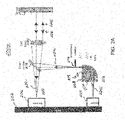
- FIG. 1 an illustration of an illustrative logistics environment 100 in which a conveyer belt 102 operates to move objects 104a-104n (collectively 104), in this case water bottles, that are sensed by a coaxial photoelectric sensor is shown.
- a photoelectric sensor or optical sensor 106 may be optically aligned with a target reflector component 108 such that an incident illumination signal 110i generated by the optical sensor 106 may be coaxially reflected back to the optical sensor 106 as a reflected illumination signal 110r .
- the target reflector component 108 may be an optical component that is part of the optical sensor or an object (e.g., water bottle) that is being sensed or inspected, for example.
- the object may coaxially reflect the incident illumination signal 110i as opposed to enabling the incident illumination signal 110i to pass therethrough if the object is opaque, reflective, or has other non-transparent properties.
- the target reflector component 108 may be an optical component, but transition to an object in the event that the object moves in front of the optical component until the object move past the sensor 106 at which time the target reflector component 108 transitions back to the optical component.
- a clear, translucent, and/or transparent object such as a water bottle, may be detected, especially if the incident illumination signal 110i is polarized, as further described herein.
- Objects that are not clear, translucent, or transparent may, of course, be detected using the optical sensor 106 and target reflector component 108 configuration.
- a logistics environment 100 is shown, it should be understood that there are many other environments, such as a manufacturing inspection system, in which the photoelectric sensor 106 may be utilized to inspect and/or sense objects.
- Coaxial sensors are fundamental in applications where the two optical paths (emitter and receiver) should coincide, for example, in applications where the sensor should be aligned with holes or small apertures or when the target should be able to work at really close distances.
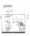
- the sensor 200a includes a printed circuit board (PCB) 202 that includes an optical emitter 204 and an optical sensor or receiver 206.
- PCB printed circuit board
- the optical emitter 204 and optical receiver 206 are coplanar and additional hardware and manufacturing processes to install the hardware and align an emitter and receiver are eliminated, thereby reducing cost and complexity of the sensor 200a.
- the optical emitter 204 may be a photodiode (e.g., LED) or laser, for example.
- a total internal reflection (TIR) optical component or lens 208 is optically aligned with the optical emitter 204.
- the TIR optical component 208 may be a lens that includes a curved profile 210 with a second surface or internal curved surface 212 that reflects incident light beams received via a first surface or incident sidewall 213a and exits via a third surface or exit sidewall 213b.
- the TIR optical component 208 is configured with a focal plane 214 at which a focal point 216 is formed, thereby operating as a virtual source (i.e., a spot in space from which illumination signals appear to irradiate).
- the virtual source at the focal point 216 has substantially the same optical performance of a light source placed on a plane at 90 degrees compared to the optical emitter 204. In being substantially the same, any optical losses due to reflection or otherwise would be lost as compared to the optical performance of the optical emitter 204.
- the virtual source is perpendicular or 90° with respect to an axis of the receiver 206.
- the focal plane 214 may include a structure 217 that serves as a diaphragm or opening (e.g., iris) within which the focal point 216 is formed.
- the focal point 216 may be larger than the opening of the structure 217, thereby enabling shaping of the virtual light source.
- the structure may operate to eliminate spurious illumination signals that might otherwise pass from the TIR optical component 208 directly or indirectly to the receiver 206.
- a reflective optical component 218 is optically aligned with the total internal reflection optical component 208.
- the reflective optical component 218 may be a beam splitter that reflects an illumination signal at one angle and enables an illumination signal to pass through the beam splitter at a different angle.
- the reflective optical component 218 may be a polarizing beam splitter, a polarizing bandpass filter, or a mirror with a hole to prevent blocking the illumination signal of both photoelements 204 and 206.
- the reflective optical component 218 may be any other optical component that performs the same or similar function of the reflective optical component 218, as further described herein.
- an exit lens 220 may be provided at an output port of the sensor 200a, and be configured to collimate an optical signal so as to be perpendicularly output from the sensor 200a.
- a target reflector component 222 is optically aligned with the reflective optical component 218 so as to coaxially reflect an illumination signal received from the reflective optical component 218.
- the optical detector 206 disposed on the PCB 202 is configured to generate an electrical signal in response to receiving an illumination signal.
- the optical detector 206 may be a single detector element or include multiple detector elements (e.g., 1D array or 2D matrix).
- the optical detector 206 may be photodiode, a position sensitive device, an avalanche photodiode, or a photodiode array.
- the optical path from the exit lens 220 to the optical detector 206 has the same length or substantially the same length (i.e., within an optical tolerance to as to have the same performance as being the same length) as the optical path from the focal point 216 of the virtual source to the exit lens 220.
- the design of the TIR optical component may be designed with a few different design features, including: (i) an incidence angle on the internal reflection surface 212, material of the TIR optical component 208, and wavelength of the optical emitter 204.
- ⁇ * ⁇ sin ⁇ 1 n 2 ⁇ n 1 ⁇
- the TIR optical component is made with a material n 1 ( ⁇ ) > n 2 ( ⁇ ) .
- the TIR optical component 208 may be plastic (e.g., PMMA, polycarbonate or cycloolefin, such as Zeonex). Other materials may be utilized, as well.
- the critical angle may be about 42.2° and about 39.2° for PMMA and polycarbonate, respectively. In being about 42.2° and about 39.2°, the incident angle on the curved surface 210 is to be wider than the critical angle for the material used to make the TIR optical component 208. Wider ranges of critical angles are also possible, such as 38°-46°.
- the internal curved surface 212 of the TIR optical component 208 may also operate properly with an incidence angle of 45°. As such, it is also possible that other incidence angles may be used, but that the other solutions may necessitate optical configurations that consume more space.
- the optical emitter 204 emits an incident illumination signal or light beam 224i into the TIR optical component 208 via the incident sidewall 213a then the beam 224i totally reflects from the internal curved surface 210 and exits via the exit sidewall 213b.
- the illumination signal 224i may be any wavelength produced by an optical emitter, and have a beamwidth that is totally internally reflected from the internal curved surface 210. As shown, the illumination signal 224i is focused to a focal point 216 at the focal plane 214, which effectively acts as a virtual source.
- the incident illumination signal 224i is shown to be reflected from the reflective optical component 218, which is collimated into parallel beams by the exit lens 220.
- the collimated incident illumination signal 224i reflects from the target reflector component 222 as a reflected illumination signal 224r .
- the reflected illumination signal 224r passes through the exit lens 220 and is focused to a focal point 225 on the optical receiver 206 via the reflective optical component 218. Because the distance between the focal point 216 of the virtual source to the exit lens 220 may be the same or substantially the same (e.g., within a few microns), the number of optical components and supporting hardware may be reduced as compared to a configuration in which the distances are not matched.
- the sensor 200b includes many of the same optical components as the coaxial photoelectric sensor 200a, but includes additional components and alternative components to support additional functions and features.
- the sensor 200b is shown to include a structure 226 defining an opening 227 through which the incident illumination signal 224i passes.
- the opening 227 is an iris, optionally dynamically adjustable, that may be shaped, as desired, and may prevent spurious illumination signals from entering the sensor 200b.
- the opening 227 may be circular or any other shape.
- Reflective optical components may be a polarizing beam splitter 228 and retroreflector 230.
- the polarizing beam splitter 228 may filter the incident optical signal 224i so as to generate a polarizing incident optical signal 224i p
- the retroreflector 230 may be configured to rotate the polarized incident illumination signal 224i p that is collimated by the exit lens 220 by 90 degrees to produce a reflected polarized illumination signal 224r p
- an inferential or bandpass filter 232 may be configured to filter the reflected polarized illumination signal 224r p to produce a filtered reflected polarized illumination signal 224r pf prior to the signal 224r p illuminating the optical receiver 206.
- the bandpass filter 232 ambient or other light that is received by the sensor 200b may be reduced or eliminated, thereby improving operation of the sensor 200b.
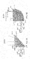
- an optical emitter 302 is shown to be in optical communication with a prism-like light guide 302.
- the prism-like light guide 304 includes a straight wall 306 with an inside surface 308 that may reflect optical signals.
- the prism-like light guide 304 includes a first sidewall 309a and a second sidewall 309b through which incident optical signals 310a, 310b, and 310c (collectively 310) are shown to pass.
- incident optical signals 310a and 310c that impinge the second surface 308 at incidence angles ⁇ and ⁇ are lost as a result of not being directed to the reflective optical element 218 (see FIG. 2 ).
- incident angles ⁇ may provide for an angle that may be used within an optical path, as a result of each of the incident angles ⁇ , ⁇ , and ⁇ being different
- the use of a prism with a second surface 308 that is flat generally precludes the use of such an optical element.
- a prism with a flat reflection surface lengthens the optical path of the incident optical signal 310 with respect to the reflected optical signal (not shown) making it impossible to use a common exit lens to collimate both the incident optical signal and reflected optical signal.
- FIG. 3B an illustration of an optical configuration 300b that includes a total internal reflection optical component or curved light guide 310 similar to or identical to the TIR optical component 208 of FIG. 2 is shown.
- the TIR optical component 310 includes a curved profile 312 that provides a second sidewall 314b that enables every point to an incidence angle ⁇ that is greater than the critical angle that maximizes the reflected energy of an incident optical signals 316a-316c (collectively 316).
- the curved profile 312 may be elliptical or parabolic, for example.
- the incident optical signals 316 enter the TIR optical component 310 via a first sidewall 314a and exits via a third sidewall 314c.
- each of the incident optical signals 316 is incident on the curved second sidewall 314b with an incidence angle ⁇ , each of the incident optical signals 316 is reflected to a common focal point 318 that effectively becomes an LED virtual image on a focal plane 320.
- the use of a curved light guide 310 allows tuning of the optical features, such as optical power and spot size outside the exit lens (see FIGS. 2A and 2B ).
- the sensor 400a includes many of the same optical components as previously presented reflective photoelectric sensors, but includes additional components and alternative components to support additional and/or alternative functions and features.
- the sensor 400a includes a printed circuit board (PCB) 402 that includes an optical emitter 404 and an optical detector or receiver 406.
- PCB printed circuit board
- the optical emitter 404 and optical receiver 406 are coplanar and additional positioning hardware and manufacturing processes to install the positioning hardware and align an emitter and receiver are eliminated, thereby reducing cost and complexity of the sensor 400a.
- the optical emitter 404 may be a photodiode or laser, for example.
- a total internal reflection optical component or lens 408a is optically aligned with the optical emitter 404.
- the TIR optical component 408a may be a lens that includes a curved profile 410a having an elliptical shape with a second surface or internal curved surface 412a that reflects incident light beams received via a first surface or incident sidewall 413a and exits via a third surface or exit sidewall 413b.
- the TIR optical component 408a is configured with a focal plane 414 at which the elliptically shaped curved profile 410a causes a focal point 416 to be formed, thereby operating as a virtual source (i.e., a spot in space from which illumination signals appear to emanate).
- the virtual source is perpendicular or 90° with respect to an axis of the receiver 406.
- the focal plane 414 may include a structure 417a defined by an iris or an opening 415a within which the focal point 416 is formed.
- the opening 415a may be circular or any other shape and have first dimensions.
- the focal point 416 may be larger than the opening of the structure 417a, thereby shaping the virtual light source.
- the structure 417a may operate to eliminate spurious illumination signals that might otherwise pass from the TIR optical component 408a directly or indirectly to the receiver 406.
- the reflective optical component 418 may be a partially reflecting mirror, a polarizing beam splitter, a polarizing bandpass filter, or a mirror with a hole, as further provided herein with regard to FIGS. 5A-5C .
- the reflective optical component 418 may be any other optical component that performs the same or similar function of the reflective optical component 418, as further described herein.
- an exit lens 420 may be provided at an output port of the sensor 400a, and be configured to collimate an optical signal so as to be perpendicularly output from the sensor 400a.
- a target reflector optical component 422 is optically aligned with the reflective optical component 418 so as to coaxially reflect an illumination signal received from the reflective optical component 418.
- the optical detector 406 disposed on the PCB 402 is configured to generate an electrical signal in response to receiving an illumination signal.
- the optical detector 406 may be a single element or include multiple detector elements (e.g., 1D array or 2D matrix).
- the optical detector 406 may be a photodiode, a position sensitive device, an avalanche photodiode, or a photodiode array.
- the optical path from the exit lens 420 to the optical detector 406 has the same length as the optical path from the focal point 416 of the virtual source to the exit lens 420, thereby minimizing optical components positioning hardware.
- an inferential or bandpass filter 426 may be configured to filter the reflected illumination signal 424r p to generate a filtered reflected illumination signal 424r pf prior to the signal 424r p illuminating the optical receiver 406.
- the bandpass filter 426 By including the bandpass filter 426, ambient or other light that is received by the sensor 400b may be reduced or eliminated, thereby improving operation of the sensor 400b.
- a TIR optical component 408b has a curved profile 410b with a parabolic shape that causes incident illumination signals 428i to reflect in a parallel manner from an internal curved surface 412b as opposed to having a focal point 416 of FIG. 4A .
- a structure 417b may define a wider opening 415b than the opening 415a of the structure 417a.
- a lens 430 may be disposed prior to the optical receiver 406. It should be understood that the configuration of the sensors 400a and 400b are illustrative and that alternative optical configurations may be utilized to perform the same or similar functions.
- the incident illumination signals 424i and 428i should be perpendicular to the incident and exit sidewalls 413a and 413b. It should be understood that the same result may be achieved using a curved mirror (e.g., with an elliptical shape) instead of using a TIR optical component 408b. As understood, however, metallization of a curved surface is a more expensive process than plastic lens manufacturing so a TIR optical component formed of plastic or other non-metalized material with a curved surface may be used for reduced cost. However, despite the added cost, such a configuration is possible, as provided in FIG. 4C .
- the sensor 400c includes the PCB 402 with the emitter 404 and receiver 406 disposed on one side thereon.
- a metallic mirror 432 may be utilized.
- the metallic mirror 432 may have a reflective surface 433 from which an incident optical signal 434i is reflected.
- the metallic mirror 432 may be curved profile, such as an elliptically shaped profile, that results in the virtual secondary light source at the focal point 416, as previously described.
- FIG. 4D an illustration of another alternative coaxial photoelectric sensor 400d is shown.
- the sensor 400d is the same as the sensor 400c with the exception that a base structure 436 to which the metallic mirror 432 is attached, and that may define a structure 417c or have the structure 417c attached thereto to enable the incident optical signal 434i to form a virtual secondary light source at the focal point 416.
- the use of the base structure 436 may simplify assembly of the sensor 400d as the base structure may be mounted to a housing 438 of the sensor.
- FIGS. 5A-5C illustrations of alternative configurations of optical components 500a-500c of a coaxial photoelectric sensor are shown.
- FIG. 5A includes a first polarizer optical component 502, mirror 504 with an opening 505, and second polarizer optical component 506.
- the first polarizer optical component 502 may be configured to polarize an incident optical signal 508i to produce a polarized incident optical signal 508i p so as to enable optical signals with a certain polarization and reduce or eliminate optical signals not in that polarization.
- vertically polarized optical signals pass through the first polarizer optical component 502 and non-vertically polarized optical signals are reduced or eliminated from passing through the component 502.
- a reflected optical signal 508r may reflect from a reflective target optical component and pass through the opening 505 defined by the mirror 504.
- the opening 505, of course, is sided and shaped to enable the reflected optical signal 508r to pass and optionally be shaped by the opening 505.
- the reflected optical signal 508r is offset sufficiently so as to pass through the opening 505.
- the reflected optical signal 508r may thereafter be filtered by the second polarizer optical component 506 so as to produce a polarized reflected optical signal 508r p that filters out ambient optical signals and/or any optical signals of the reflected optical signal 508r not aligned with the polarization of the second polarizer optical component 506.
- the polarized reflected optical signal 508r p may thereafter be applied to an optical detector (see FIGS. 4A and 4B ), as previously described.
- a beam splitter 510 is used to reflect the polarized incident optical signal 508i p and also pass the polarized reflected optical signal 508r p .
- This configuration of optical components 500b provides for the same polarization processing of the incident and reflected optical signals 508i p and 508r p as the configuration of optical components 500a.
- the configuration of optical components 500c provides for eliminating the first and second polarized optical components 502 and 506 used in FIGS. 5A and 5B , and uses a polarizing beam splitter (or polarizing bandpass filter) 512 to reflect a certain polarization so that a polarized incident optical signal 508i p results and a polarized reflected optical signal 508r p is received after reflection.
- the polarizing beam splitter 512 reflects one of the s- or p-polarization electric fields and transmits the other.
- the polarized reflected optical signal 508r p passes through the polarizing beam splitter 512.
- the polarized reflected optical signal 508r p is polarized in an opposite manner due to being reflected by a retroreflector, which enables the polarized reflected optical signal 508r p to pass through the filter (see FIG. 4A ) with minimal loss prior to impinging the optical sensor (see FIG. 4A ).
- the configuration of optical components 500c minimizes the number of optical components, which may also allow for the least number of assembly components and steps for manufacturing a coaxial photoelectric sensor.
- the coaxial photoelectric sensing process 600 starts at step 602, where an incident illumination signal is generated.
- the incident illumination signal may be produced by an LED or laser.
- the illumination signal is first reflected, such as totally internally reflecting, so as to cause the incident illumination signal to be a first reflected illumination signal and routed along an optical path by 90 degrees at step 604. It should be understood that alternative angles may be utilized depending on the configuration of the sensor.
- the first reflected illumination signal is second reflected to produce a second reflected illumination signal.
- the reflection may be performed by a number of different types of reflective optical components, such as a mirror that defines an opening through with a coaxial reflection may traverse, a beam splitter, a polarizing beam splitter, or otherwise.
- the second reflected illumination signal is coaxially reflected.
- the coaxial reflection may be performed by a reflective optical component, such as a target optical component, retroreflector, or otherwise.
- the coaxial reflection enables the sensor to sense a transparent object passed between an exit port of the sensor (i.e., after the reflective optical component) and the target reflective optical component optically aligned to coaxially reflect the incident illumination signal.
- an electrical signal is generated in response to receiving the coaxially reflected illumination signal.
- the electrical signal may be generated by an optical detector, such as a photodiode or other photoelectric device, as previously described herein.
- a lens may be utilized to both collimate the incident illumination signal and focus the coaxially reflected illumination signal onto the optical detector.
- first reflecting the illumination signal includes totally internally reflecting the illumination signal optionally using a light guide.
- coaxially reflecting the second reflected illumination signal includes reflecting the second reflected illumination signal using a retroreflector.
- First reflecting the illumination signal includes causing the illumination signal to be focused at a focal plane to produce a virtual secondary illumination source.
- Second reflecting the first reflected illumination signal may include reflecting the first reflected illumination signal using a beam splitter.
- using a beam splitter may include using a polarizing beam splitter.
- coaxially reflecting the totally internally reflected illumination signal may include retroreflecting the second reflected illumination signal to cause polarization of the illumination signal to be rotated by 90°.
- the process 600 may further include interference filtering the coaxially reflected illumination signal.
- the process 600 may further include collimating the reflected totally internally reflected illumination signal.
- a flow diagram of a manufacturing process 700 of a coaxial photoelectric sensor is shown.
- the process 700 starts at step 702, where an optical emitter is disposed on a printed circuit board (PCB).
- the optical emitter is configured to generate an illumination signal.
- a reflection optical component is optically aligned with the optical emitter to receive and reflect the illumination signal to produce a first reflected illumination signal.
- a reflective optical component is optically aligned with the reflection optical component so as to receive the first reflected illumination signal received from the reflection optical component at step 706 and produce a second reflected illumination signal.
- a target reflector component is optically aligned with the reflective optical component to coaxially reflect the second illumination signal received from the reflective optical component.
- an optical detector is disposed on the PCB to generate an electrical signal in response to receiving the illumination signal coaxially reflected by the target reflector component.
- an aperture may be placed or positioned at the exit of an LED window or on an LED virtual image plane after the TIR lens.
- Both of the configurations enable tuning of a size of a light spot by shrinking or enlarging a diaphragm aperture, but just the latter configuration allows the definition of a more precise spot filtered from optical aberrations, multiple reflections inside the TIR lens, and deformations due to unavoidable mold imperfections.
- the diaphragm may be manufactured with an external metallic or plastic foil or may be integrated in the design of an optical camera or may be directly realized on a third or exit surface of the TIR lens (e.g., with pad printing or painting using a mask or other technologies).
- the configuration of the photoelectric sensors may create a virtual source oriented 90° with respect to a receive axis (i.e., axis of the optical detector), but both of the photoelements may be positioned on the same side of a PCB.
- a total number of PCBs may be saved, and an optics function of the sensor can be specialized in early stages of production, thereby making the production flow more uniform.
- the shape of the sensed optical signal or light spot which is controlled by the shape of the virtual light source, may be performed by varying an iris aperture with different geometries so as to realize the same optical function as conventional coaxial sensors, but using fewer opto-mechanical parts than conventional coaxial sensors.
- coaxial photoelectric sensor features described herein may be utilized in non-polarized and polarized coaxial photoelectric sensors for the detection of transparent, opaque, and/or reflective targets.
- a single light spot may be illuminated onto an optical sensor, and, therefore, a PSD or a photodiode array may be used as a detector, which may be useful because a new range of potential applications as a result of the detection of tilt of a target may be sensed.
- cost may be reduced.
- the use of a virtual light source, as provided herein provides a more uniform and well-defined light spot that is useful for customer applications.
Landscapes
- Physics & Mathematics (AREA)
- General Physics & Mathematics (AREA)
- Engineering & Computer Science (AREA)
- Life Sciences & Earth Sciences (AREA)
- General Life Sciences & Earth Sciences (AREA)
- Geophysics (AREA)
- Computer Networks & Wireless Communication (AREA)
- Radar, Positioning & Navigation (AREA)
- Remote Sensing (AREA)
- Optical Radar Systems And Details Thereof (AREA)
Claims (13)
- Koaxialer photoelektrischer Sensor (106, 200a, 200b, 400a, 400b, 400c, 400d), der Folgendes umfasst:einen optischen Emitter (204, 404), der auf einer gedruckten Leiterplatte (PCB) (202, 402) angeordnet und so konfiguriert ist, dass er ein Beleuchtungssignal erzeugt;eine optische Reflexionskomponente (208, 310, 408a, 408b, 432), die optisch mit dem optischen Emitter (204, 404) ausgerichtet ist, um das Beleuchtungssignal zu empfangen und zu reflektieren, um ein erstes reflektiertes Beleuchtungssignal zu erzeugen;eine reflektierende optische Komponente (218, 228, 418, 504, 510, 512), die optisch mit der reflektierenden optischen Komponente (208, 310, 408a, 408b, 432) ausgerichtet ist, um das von der reflektierenden optischen Komponente (208, 310, 408a, 408b, 432) empfangene erste reflektierte Beleuchtungssignal zu reflektieren, um ein zweites reflektiertes Beleuchtungssignal zu erzeugen;eine Zielreflektorkomponente (104a, 108, 222, 230, 422), die optisch mit der reflektierenden optischen Komponente (218, 228, 418, 504, 510, 512) ausgerichtet ist, um das von der reflektierenden optischen Komponente (218, 228, 418, 504, 510, 512) empfangene zweite reflektierte Beleuchtungssignal koaxial zu reflektieren; undeinen optischen Detektor (206, 406), der auf der Leiterplatte (202, 402) angeordnet und so konfiguriert ist, dass er als Reaktion auf den Empfang des von der Zielreflektorkomponente (104a, 108, 222, 230, 422) koaxial reflektierten Beleuchtungssignals ein elektrisches Signal erzeugt, dadurch gekennzeichnet, dass die optische Reflexionskomponente (208, 310, 408a, 408b, 432) so konfiguriert ist, dass sie bewirkt, dass das erste reflektierte Beleuchtungssignal in einer Brennebene (214, 320, 414) zwischen der optischen Reflexionskomponente (208, 310, 408a, 408b, 432) und der reflektierenden optischen Komponente (218, 228, 418, 504, 510, 512) fokussiert wird, wodurch eine virtuelle sekundäre Beleuchtungsquelle (216, 318, 416) in der Brennebene erzeugt wird.
- Sensor (106, 200a, 200b, 400a, 400b, 400c, 400d) nach Anspruch 1, der ferner eine Austrittslinse (220, 420) umfasst, und wobei (i) eine Länge eines optischen Weges zwischen der Austrittslinse (220, 420) und dem optischen Detektor (206, 406) und (ii) eine Länge des optischen Weges zwischen der Austrittslinse (220, 420) und der virtuellen sekundären Lichtquelle (216, 318, 416) ungefähr gleich sind.
- Sensor (106, 200a, 200b, 400a, 400b, 400c, 400d) nach einem der Ansprüche 1 bis 2, wobei die optische Reflexionskomponente (208, 310, 408a, 408b, 432) eine optische Komponente mit totaler interner Reflexion (208, 310, 408a, 408b) oder ein gekrümmter Spiegel (432) ist.
- Sensor (106, 200a, 200b, 400a, 400b, 400c, 400d) nach einem der Ansprüche 1 bis 3, wobei die Zielreflektorkomponente (104a, 108, 222, 230, 422) ein Retroreflektor (230) und/oder ein zu untersuchendes Objekt (104a) ist.
- Sensor (106, 200b, 400a, 400b, 400c, 400d) nach einem der Ansprüche 1 bis 4, der ferner ein Interferenzfilter (232, 426) umfasst, das optisch zwischen der reflektierenden optischen Komponente (228, 418) und dem optischen Detektor (206, 406) ausgerichtet ist.
- Sensor (106, 200a, 200b, 400a, 400c, 400d) nach einem der Ansprüche 1-5, der ferner eine Kollimationslinse (220, 420) umfasst, die zwischen der reflektierenden optischen Komponente (218, 418) und der Zielreflektorkomponente (222, 422) angeordnet ist.
- Sensor (106, 200a, 200b, 400a, 400b, 400c, 400d) nach Anspruch 1, der ferner eine Blende (217, 227, 417a) umfasst, die in einer Brennebene (214, 414) der optischen Reflexionskomponente (208, 310, 408a, 408b, 432) angeordnet ist.
- Verfahren zur koaxial photoelektrischen Abtastung, das Folgendes umfasst:Erzeugen eines Beleuchtungssignals;Erste Reflexion des Beleuchtungssignals, um ein erstes reflektiertes Beleuchtungssignal zu erzeugen;Zweite Reflexion des ersten reflektierten Beleuchtungssignals zur Erzeugung eines zweiten reflektierten Beleuchtungssignals;Koaxial Reflektieren des zweiten reflektierten Beleuchtungssignals; undErzeugen eines elektrischen Signals in Reaktion auf den Empfang des koaxial reflektierten Beleuchtungssignals, dadurch gekennzeichnet, dass das erste Reflektieren des Beleuchtungssignals umfasst Fokussieren des ersten reflektierten Beleuchtungssignals auf eine Brennebene vor dem zweiten Reflektieren des ersten reflektierten Beleuchtungssignals, wodurch eine virtuelle sekundäre Beleuchtungsquelle in der Brennebene erzeugt wird.
- Verfahren nach Anspruch 8, das ferner umfasst Kollimieren des zweiten reflektierten Beleuchtungssignals vor dem koaxial Reflektieren des zweiten reflektierten Beleuchtungssignals, und wobei eine Länge eines optischen Weges zwischen einer Ebene, an der das Kollimieren stattfindet, und einer Ebene, an der das koaxial reflektierte Beleuchtungssignal empfangen wird, im Wesentlichen dieselbe ist wie eine Länge eines optischen Weges zwischen der Ebene, an der das Kollimieren stattfindet, und der Brennebene.
- Verfahren nach einem der Ansprüche 8 bis 9, wobei das erste Reflektieren des Beleuchtungssignals die vollständige interne Reflexion des Beleuchtungssignals oder die erste Reflexion des Beleuchtungssignals unter Verwendung eines gekrümmten Spiegels umfasst.
- Verfahren nach einem der Ansprüche 8 bis 10, wobei die koaxiale Reflexion des zweiten reflektierten Beleuchtungssignals die Rückreflexion des zweiten reflektierten Beleuchtungssignals und/oder die koaxiale Reflexion des zweiten reflektierten Beleuchtungssignals durch ein zu untersuchendes Objekt umfasst.
- Verfahren nach einem der Ansprüche 8 bis 11, das ferner die Interferenzfilterung des koaxial reflektierten Beleuchtungssignals umfasst.
- Verfahren nach einem der Ansprüche 8 bis 12, das ferner Kollimieren des zweiten reflektierten Beleuchtungssignals umfasst.
Applications Claiming Priority (1)
| Application Number | Priority Date | Filing Date | Title |
|---|---|---|---|
| US16/451,456 US11163090B2 (en) | 2019-06-25 | 2019-06-25 | Photoelectric sensor with coaxial emission and receiving optical paths |
Publications (2)
| Publication Number | Publication Date |
|---|---|
| EP3757604A1 EP3757604A1 (de) | 2020-12-30 |
| EP3757604B1 true EP3757604B1 (de) | 2022-09-07 |
Family
ID=71143632
Family Applications (1)
| Application Number | Title | Priority Date | Filing Date |
|---|---|---|---|
| EP20182164.2A Active EP3757604B1 (de) | 2019-06-25 | 2020-06-25 | Photoelektrischer sensor mit koaxialen emissions- und optischen empfangswegen |
Country Status (2)
| Country | Link |
|---|---|
| US (1) | US11163090B2 (de) |
| EP (1) | EP3757604B1 (de) |
Families Citing this family (1)
| Publication number | Priority date | Publication date | Assignee | Title |
|---|---|---|---|---|
| US20240069170A1 (en) * | 2022-08-26 | 2024-02-29 | Luminar Technologies, Inc. | Small aperture optical periscope for lidar |
Family Cites Families (11)
| Publication number | Priority date | Publication date | Assignee | Title |
|---|---|---|---|---|
| US4346292A (en) * | 1981-02-02 | 1982-08-24 | International Business Machines Corporation | Coaxial optical scanner |
| US6114712A (en) * | 1996-10-09 | 2000-09-05 | Symbol Technologies, Inc. | One piece optical assembly for low cost optical scanner |
| US6084998A (en) * | 1998-12-30 | 2000-07-04 | Alpha And Omega Imaging, Llc | System and method for fabricating distributed Bragg reflectors with preferred properties |
| JP3578214B2 (ja) | 2002-12-09 | 2004-10-20 | オムロン株式会社 | 回帰反射型光電センサ |
| JP2005164261A (ja) | 2003-11-28 | 2005-06-23 | Sunx Ltd | 同軸反射型光電センサ |
| JPWO2006016504A1 (ja) | 2004-08-09 | 2008-05-01 | オムロン株式会社 | 光電センサ用の光学素子およびこれを用いた光電センサ |
| JP4158828B2 (ja) | 2006-10-30 | 2008-10-01 | オムロン株式会社 | 回帰反射型光電センサ、回帰反射型光電センサのセンサ本体および回帰反射部 |
| JP5266859B2 (ja) | 2008-04-25 | 2013-08-21 | オムロン株式会社 | 光電センサ |
| DE102009055989B4 (de) | 2009-11-20 | 2017-02-16 | Faro Technologies, Inc. | Vorrichtung zum optischen Abtasten und Vermessen einer Umgebung |
| DE202012010432U1 (de) | 2012-10-26 | 2012-11-09 | Sensopart Industriesensorik Gmbh | Optischer Sensor |
| JP6990864B2 (ja) * | 2017-10-20 | 2022-01-12 | パナソニックIpマネジメント株式会社 | 距離測定装置 |
-
2019
- 2019-06-25 US US16/451,456 patent/US11163090B2/en active Active
-
2020
- 2020-06-25 EP EP20182164.2A patent/EP3757604B1/de active Active
Also Published As
| Publication number | Publication date |
|---|---|
| EP3757604A1 (de) | 2020-12-30 |
| US11163090B2 (en) | 2021-11-02 |
| US20200408948A1 (en) | 2020-12-31 |
Similar Documents
| Publication | Publication Date | Title |
|---|---|---|
| JP7501864B2 (ja) | コリメートを行うカバー要素によって覆われたスキャンミラーを備えた送信器 | |
| JP7312979B2 (ja) | レーザートランシーバーモジュールおよびその光学調整方法、レーザーレーダーおよび自動運転装置 | |
| KR20230126704A (ko) | 전송 광학 전력 모니터를 사용하는 LiDAR 시스템 | |
| KR101806753B1 (ko) | 스캐닝 엔진에 대한 모듈식 광학계 | |
| CN103576133A (zh) | 距离测量系统 | |
| US10382642B2 (en) | Image reading apparatus | |
| CN110132544B (zh) | 一种光学测试设备 | |
| CN107576394B (zh) | 用于限定对光谱仪的入射角的装置和运行该装置的方法 | |
| US20100046057A1 (en) | Micro electronic mechanical system oscillating laser scanning unit | |
| US20040136100A1 (en) | Optical sensor | |
| EP3757604B1 (de) | Photoelektrischer sensor mit koaxialen emissions- und optischen empfangswegen | |
| KR101895593B1 (ko) | 광학 검사 시스템 및 광학 이미징 시스템 | |
| CN104864892B (zh) | 光电传感器 | |
| JP2020182165A (ja) | 画像読取装置 | |
| US6946643B1 (en) | Retro-reflective photoelectric sensor | |
| US7417217B2 (en) | Regressive reflection type photoelectric switch | |
| CN111656214A (zh) | 光学雷达装置 | |
| US6715683B2 (en) | Optical data code reader | |
| CN221465737U (zh) | 激光雷达 | |
| CN112415740A (zh) | 一种结构光控制装置 | |
| US20220397756A1 (en) | Optical scanning device | |
| US5033844A (en) | Camera employing automatic focusing unit | |
| JP6798262B2 (ja) | 光学ユニット及び測距センサ | |
| CN223244813U (zh) | 激光雷达 | |
| US11579257B2 (en) | Scanning LiDAR system and method with unitary optical element |
Legal Events
| Date | Code | Title | Description |
|---|---|---|---|
| PUAI | Public reference made under article 153(3) epc to a published international application that has entered the european phase |
Free format text: ORIGINAL CODE: 0009012 |
|
| STAA | Information on the status of an ep patent application or granted ep patent |
Free format text: STATUS: THE APPLICATION HAS BEEN PUBLISHED |
|
| AK | Designated contracting states |
Kind code of ref document: A1 Designated state(s): AL AT BE BG CH CY CZ DE DK EE ES FI FR GB GR HR HU IE IS IT LI LT LU LV MC MK MT NL NO PL PT RO RS SE SI SK SM TR |
|
| AX | Request for extension of the european patent |
Extension state: BA ME |
|
| STAA | Information on the status of an ep patent application or granted ep patent |
Free format text: STATUS: REQUEST FOR EXAMINATION WAS MADE |
|
| 17P | Request for examination filed |
Effective date: 20210630 |
|
| RBV | Designated contracting states (corrected) |
Designated state(s): AL AT BE BG CH CY CZ DE DK EE ES FI FR GB GR HR HU IE IS IT LI LT LU LV MC MK MT NL NO PL PT RO RS SE SI SK SM TR |
|
| GRAP | Despatch of communication of intention to grant a patent |
Free format text: ORIGINAL CODE: EPIDOSNIGR1 |
|
| STAA | Information on the status of an ep patent application or granted ep patent |
Free format text: STATUS: GRANT OF PATENT IS INTENDED |
|
| INTG | Intention to grant announced |
Effective date: 20220413 |
|
| GRAS | Grant fee paid |
Free format text: ORIGINAL CODE: EPIDOSNIGR3 |
|
| GRAA | (expected) grant |
Free format text: ORIGINAL CODE: 0009210 |
|
| STAA | Information on the status of an ep patent application or granted ep patent |
Free format text: STATUS: THE PATENT HAS BEEN GRANTED |
|
| AK | Designated contracting states |
Kind code of ref document: B1 Designated state(s): AL AT BE BG CH CY CZ DE DK EE ES FI FR GB GR HR HU IE IS IT LI LT LU LV MC MK MT NL NO PL PT RO RS SE SI SK SM TR |
|
| REG | Reference to a national code |
Ref country code: GB Ref legal event code: FG4D |
|
| REG | Reference to a national code |
Ref country code: CH Ref legal event code: EP Ref country code: AT Ref legal event code: REF Ref document number: 1517505 Country of ref document: AT Kind code of ref document: T Effective date: 20220915 |
|
| REG | Reference to a national code |
Ref country code: DE Ref legal event code: R096 Ref document number: 602020004917 Country of ref document: DE |
|
| REG | Reference to a national code |
Ref country code: IE Ref legal event code: FG4D |
|
| REG | Reference to a national code |
Ref country code: DE Ref legal event code: R081 Ref document number: 602020004917 Country of ref document: DE Owner name: DATALOGIC IP TECH S.R.L., IT Free format text: FORMER OWNER: DATALOGIC IP TECH S.R.L., CALDERARA DI RENO, IT |
|
| REG | Reference to a national code |
Ref country code: LT Ref legal event code: MG9D |
|
| REG | Reference to a national code |
Ref country code: NL Ref legal event code: MP Effective date: 20220907 |
|
| PG25 | Lapsed in a contracting state [announced via postgrant information from national office to epo] |
Ref country code: SE Free format text: LAPSE BECAUSE OF FAILURE TO SUBMIT A TRANSLATION OF THE DESCRIPTION OR TO PAY THE FEE WITHIN THE PRESCRIBED TIME-LIMIT Effective date: 20220907 Ref country code: RS Free format text: LAPSE BECAUSE OF FAILURE TO SUBMIT A TRANSLATION OF THE DESCRIPTION OR TO PAY THE FEE WITHIN THE PRESCRIBED TIME-LIMIT Effective date: 20220907 Ref country code: NO Free format text: LAPSE BECAUSE OF FAILURE TO SUBMIT A TRANSLATION OF THE DESCRIPTION OR TO PAY THE FEE WITHIN THE PRESCRIBED TIME-LIMIT Effective date: 20221207 Ref country code: LV Free format text: LAPSE BECAUSE OF FAILURE TO SUBMIT A TRANSLATION OF THE DESCRIPTION OR TO PAY THE FEE WITHIN THE PRESCRIBED TIME-LIMIT Effective date: 20220907 Ref country code: LT Free format text: LAPSE BECAUSE OF FAILURE TO SUBMIT A TRANSLATION OF THE DESCRIPTION OR TO PAY THE FEE WITHIN THE PRESCRIBED TIME-LIMIT Effective date: 20220907 Ref country code: FI Free format text: LAPSE BECAUSE OF FAILURE TO SUBMIT A TRANSLATION OF THE DESCRIPTION OR TO PAY THE FEE WITHIN THE PRESCRIBED TIME-LIMIT Effective date: 20220907 |
|
| REG | Reference to a national code |
Ref country code: AT Ref legal event code: MK05 Ref document number: 1517505 Country of ref document: AT Kind code of ref document: T Effective date: 20220907 |
|
| PG25 | Lapsed in a contracting state [announced via postgrant information from national office to epo] |
Ref country code: HR Free format text: LAPSE BECAUSE OF FAILURE TO SUBMIT A TRANSLATION OF THE DESCRIPTION OR TO PAY THE FEE WITHIN THE PRESCRIBED TIME-LIMIT Effective date: 20220907 Ref country code: GR Free format text: LAPSE BECAUSE OF FAILURE TO SUBMIT A TRANSLATION OF THE DESCRIPTION OR TO PAY THE FEE WITHIN THE PRESCRIBED TIME-LIMIT Effective date: 20221208 |
|
| PG25 | Lapsed in a contracting state [announced via postgrant information from national office to epo] |
Ref country code: SM Free format text: LAPSE BECAUSE OF FAILURE TO SUBMIT A TRANSLATION OF THE DESCRIPTION OR TO PAY THE FEE WITHIN THE PRESCRIBED TIME-LIMIT Effective date: 20220907 Ref country code: RO Free format text: LAPSE BECAUSE OF FAILURE TO SUBMIT A TRANSLATION OF THE DESCRIPTION OR TO PAY THE FEE WITHIN THE PRESCRIBED TIME-LIMIT Effective date: 20220907 Ref country code: PT Free format text: LAPSE BECAUSE OF FAILURE TO SUBMIT A TRANSLATION OF THE DESCRIPTION OR TO PAY THE FEE WITHIN THE PRESCRIBED TIME-LIMIT Effective date: 20230109 Ref country code: ES Free format text: LAPSE BECAUSE OF FAILURE TO SUBMIT A TRANSLATION OF THE DESCRIPTION OR TO PAY THE FEE WITHIN THE PRESCRIBED TIME-LIMIT Effective date: 20220907 Ref country code: CZ Free format text: LAPSE BECAUSE OF FAILURE TO SUBMIT A TRANSLATION OF THE DESCRIPTION OR TO PAY THE FEE WITHIN THE PRESCRIBED TIME-LIMIT Effective date: 20220907 Ref country code: AT Free format text: LAPSE BECAUSE OF FAILURE TO SUBMIT A TRANSLATION OF THE DESCRIPTION OR TO PAY THE FEE WITHIN THE PRESCRIBED TIME-LIMIT Effective date: 20220907 |
|
| PG25 | Lapsed in a contracting state [announced via postgrant information from national office to epo] |
Ref country code: SK Free format text: LAPSE BECAUSE OF FAILURE TO SUBMIT A TRANSLATION OF THE DESCRIPTION OR TO PAY THE FEE WITHIN THE PRESCRIBED TIME-LIMIT Effective date: 20220907 Ref country code: PL Free format text: LAPSE BECAUSE OF FAILURE TO SUBMIT A TRANSLATION OF THE DESCRIPTION OR TO PAY THE FEE WITHIN THE PRESCRIBED TIME-LIMIT Effective date: 20220907 Ref country code: IS Free format text: LAPSE BECAUSE OF FAILURE TO SUBMIT A TRANSLATION OF THE DESCRIPTION OR TO PAY THE FEE WITHIN THE PRESCRIBED TIME-LIMIT Effective date: 20230107 Ref country code: EE Free format text: LAPSE BECAUSE OF FAILURE TO SUBMIT A TRANSLATION OF THE DESCRIPTION OR TO PAY THE FEE WITHIN THE PRESCRIBED TIME-LIMIT Effective date: 20220907 |
|
| REG | Reference to a national code |
Ref country code: DE Ref legal event code: R097 Ref document number: 602020004917 Country of ref document: DE |
|
| PG25 | Lapsed in a contracting state [announced via postgrant information from national office to epo] |
Ref country code: NL Free format text: LAPSE BECAUSE OF FAILURE TO SUBMIT A TRANSLATION OF THE DESCRIPTION OR TO PAY THE FEE WITHIN THE PRESCRIBED TIME-LIMIT Effective date: 20220907 Ref country code: AL Free format text: LAPSE BECAUSE OF FAILURE TO SUBMIT A TRANSLATION OF THE DESCRIPTION OR TO PAY THE FEE WITHIN THE PRESCRIBED TIME-LIMIT Effective date: 20220907 |
|
| P01 | Opt-out of the competence of the unified patent court (upc) registered |
Effective date: 20230525 |
|
| PLBE | No opposition filed within time limit |
Free format text: ORIGINAL CODE: 0009261 |
|
| STAA | Information on the status of an ep patent application or granted ep patent |
Free format text: STATUS: NO OPPOSITION FILED WITHIN TIME LIMIT |
|
| PG25 | Lapsed in a contracting state [announced via postgrant information from national office to epo] |
Ref country code: DK Free format text: LAPSE BECAUSE OF FAILURE TO SUBMIT A TRANSLATION OF THE DESCRIPTION OR TO PAY THE FEE WITHIN THE PRESCRIBED TIME-LIMIT Effective date: 20220907 |
|
| 26N | No opposition filed |
Effective date: 20230608 |
|
| PG25 | Lapsed in a contracting state [announced via postgrant information from national office to epo] |
Ref country code: SI Free format text: LAPSE BECAUSE OF FAILURE TO SUBMIT A TRANSLATION OF THE DESCRIPTION OR TO PAY THE FEE WITHIN THE PRESCRIBED TIME-LIMIT Effective date: 20220907 |
|
| PG25 | Lapsed in a contracting state [announced via postgrant information from national office to epo] |
Ref country code: MC Free format text: LAPSE BECAUSE OF FAILURE TO SUBMIT A TRANSLATION OF THE DESCRIPTION OR TO PAY THE FEE WITHIN THE PRESCRIBED TIME-LIMIT Effective date: 20220907 |
|
| PG25 | Lapsed in a contracting state [announced via postgrant information from national office to epo] |
Ref country code: MC Free format text: LAPSE BECAUSE OF FAILURE TO SUBMIT A TRANSLATION OF THE DESCRIPTION OR TO PAY THE FEE WITHIN THE PRESCRIBED TIME-LIMIT Effective date: 20220907 |
|
| REG | Reference to a national code |
Ref country code: CH Ref legal event code: PL |
|
| REG | Reference to a national code |
Ref country code: BE Ref legal event code: MM Effective date: 20230630 |
|
| PG25 | Lapsed in a contracting state [announced via postgrant information from national office to epo] |
Ref country code: LU Free format text: LAPSE BECAUSE OF NON-PAYMENT OF DUE FEES Effective date: 20230625 |
|
| REG | Reference to a national code |
Ref country code: IE Ref legal event code: MM4A |
|
| PG25 | Lapsed in a contracting state [announced via postgrant information from national office to epo] |
Ref country code: LU Free format text: LAPSE BECAUSE OF NON-PAYMENT OF DUE FEES Effective date: 20230625 |
|
| PG25 | Lapsed in a contracting state [announced via postgrant information from national office to epo] |
Ref country code: IE Free format text: LAPSE BECAUSE OF NON-PAYMENT OF DUE FEES Effective date: 20230625 |
|
| PG25 | Lapsed in a contracting state [announced via postgrant information from national office to epo] |
Ref country code: IE Free format text: LAPSE BECAUSE OF NON-PAYMENT OF DUE FEES Effective date: 20230625 Ref country code: CH Free format text: LAPSE BECAUSE OF NON-PAYMENT OF DUE FEES Effective date: 20230630 |
|
| PG25 | Lapsed in a contracting state [announced via postgrant information from national office to epo] |
Ref country code: FR Free format text: LAPSE BECAUSE OF NON-PAYMENT OF DUE FEES Effective date: 20230630 Ref country code: BE Free format text: LAPSE BECAUSE OF NON-PAYMENT OF DUE FEES Effective date: 20230630 |
|
| PG25 | Lapsed in a contracting state [announced via postgrant information from national office to epo] |
Ref country code: BG Free format text: LAPSE BECAUSE OF FAILURE TO SUBMIT A TRANSLATION OF THE DESCRIPTION OR TO PAY THE FEE WITHIN THE PRESCRIBED TIME-LIMIT Effective date: 20220907 |
|
| PG25 | Lapsed in a contracting state [announced via postgrant information from national office to epo] |
Ref country code: BG Free format text: LAPSE BECAUSE OF FAILURE TO SUBMIT A TRANSLATION OF THE DESCRIPTION OR TO PAY THE FEE WITHIN THE PRESCRIBED TIME-LIMIT Effective date: 20220907 |
|
| GBPC | Gb: european patent ceased through non-payment of renewal fee |
Effective date: 20240625 |
|
| PG25 | Lapsed in a contracting state [announced via postgrant information from national office to epo] |
Ref country code: GB Free format text: LAPSE BECAUSE OF NON-PAYMENT OF DUE FEES Effective date: 20240625 |
|
| PGFP | Annual fee paid to national office [announced via postgrant information from national office to epo] |
Ref country code: DE Payment date: 20250618 Year of fee payment: 6 |
|
| PG25 | Lapsed in a contracting state [announced via postgrant information from national office to epo] |
Ref country code: CY Free format text: LAPSE BECAUSE OF FAILURE TO SUBMIT A TRANSLATION OF THE DESCRIPTION OR TO PAY THE FEE WITHIN THE PRESCRIBED TIME-LIMIT; INVALID AB INITIO Effective date: 20200625 |
|
| PG25 | Lapsed in a contracting state [announced via postgrant information from national office to epo] |
Ref country code: HU Free format text: LAPSE BECAUSE OF FAILURE TO SUBMIT A TRANSLATION OF THE DESCRIPTION OR TO PAY THE FEE WITHIN THE PRESCRIBED TIME-LIMIT; INVALID AB INITIO Effective date: 20200625 |
|
| PGFP | Annual fee paid to national office [announced via postgrant information from national office to epo] |
Ref country code: IT Payment date: 20250624 Year of fee payment: 6 |
|
| PG25 | Lapsed in a contracting state [announced via postgrant information from national office to epo] |
Ref country code: TR Free format text: LAPSE BECAUSE OF FAILURE TO SUBMIT A TRANSLATION OF THE DESCRIPTION OR TO PAY THE FEE WITHIN THE PRESCRIBED TIME-LIMIT Effective date: 20220907 |