EP3757454A1 - Light emitting module - Google Patents
Light emitting module Download PDFInfo
- Publication number
- EP3757454A1 EP3757454A1 EP20182003.2A EP20182003A EP3757454A1 EP 3757454 A1 EP3757454 A1 EP 3757454A1 EP 20182003 A EP20182003 A EP 20182003A EP 3757454 A1 EP3757454 A1 EP 3757454A1
- Authority
- EP
- European Patent Office
- Prior art keywords
- light
- recessed portion
- face
- light emitting
- guide plate
- Prior art date
- Legal status (The legal status is an assumption and is not a legal conclusion. Google has not performed a legal analysis and makes no representation as to the accuracy of the status listed.)
- Granted
Links
Images



Classifications
-
- H—ELECTRICITY
- H10—SEMICONDUCTOR DEVICES; ELECTRIC SOLID-STATE DEVICES NOT OTHERWISE PROVIDED FOR
- H10H—INORGANIC LIGHT-EMITTING SEMICONDUCTOR DEVICES HAVING POTENTIAL BARRIERS
- H10H20/00—Individual inorganic light-emitting semiconductor devices having potential barriers, e.g. light-emitting diodes [LED]
- H10H20/80—Constructional details
- H10H20/85—Packages
- H10H20/855—Optical field-shaping means, e.g. lenses
-
- H—ELECTRICITY
- H10—SEMICONDUCTOR DEVICES; ELECTRIC SOLID-STATE DEVICES NOT OTHERWISE PROVIDED FOR
- H10H—INORGANIC LIGHT-EMITTING SEMICONDUCTOR DEVICES HAVING POTENTIAL BARRIERS
- H10H20/00—Individual inorganic light-emitting semiconductor devices having potential barriers, e.g. light-emitting diodes [LED]
- H10H20/80—Constructional details
- H10H20/85—Packages
-
- G—PHYSICS
- G02—OPTICS
- G02B—OPTICAL ELEMENTS, SYSTEMS OR APPARATUS
- G02B6/00—Light guides; Structural details of arrangements comprising light guides and other optical elements, e.g. couplings
- G02B6/0001—Light guides; Structural details of arrangements comprising light guides and other optical elements, e.g. couplings specially adapted for lighting devices or systems
- G02B6/0011—Light guides; Structural details of arrangements comprising light guides and other optical elements, e.g. couplings specially adapted for lighting devices or systems the light guides being planar or of plate-like form
- G02B6/0013—Means for improving the coupling-in of light from the light source into the light guide
- G02B6/0015—Means for improving the coupling-in of light from the light source into the light guide provided on the surface of the light guide or in the bulk of it
- G02B6/002—Means for improving the coupling-in of light from the light source into the light guide provided on the surface of the light guide or in the bulk of it by shaping at least a portion of the light guide, e.g. with collimating, focussing or diverging surfaces
- G02B6/0021—Means for improving the coupling-in of light from the light source into the light guide provided on the surface of the light guide or in the bulk of it by shaping at least a portion of the light guide, e.g. with collimating, focussing or diverging surfaces for housing at least a part of the light source, e.g. by forming holes or recesses
-
- G—PHYSICS
- G02—OPTICS
- G02B—OPTICAL ELEMENTS, SYSTEMS OR APPARATUS
- G02B6/00—Light guides; Structural details of arrangements comprising light guides and other optical elements, e.g. couplings
- G02B6/0001—Light guides; Structural details of arrangements comprising light guides and other optical elements, e.g. couplings specially adapted for lighting devices or systems
- G02B6/0011—Light guides; Structural details of arrangements comprising light guides and other optical elements, e.g. couplings specially adapted for lighting devices or systems the light guides being planar or of plate-like form
- G02B6/0066—Light guides; Structural details of arrangements comprising light guides and other optical elements, e.g. couplings specially adapted for lighting devices or systems the light guides being planar or of plate-like form characterised by the light source being coupled to the light guide
- G02B6/0073—Light emitting diode [LED]
-
- G—PHYSICS
- G02—OPTICS
- G02F—OPTICAL DEVICES OR ARRANGEMENTS FOR THE CONTROL OF LIGHT BY MODIFICATION OF THE OPTICAL PROPERTIES OF THE MEDIA OF THE ELEMENTS INVOLVED THEREIN; NON-LINEAR OPTICS; FREQUENCY-CHANGING OF LIGHT; OPTICAL LOGIC ELEMENTS; OPTICAL ANALOGUE/DIGITAL CONVERTERS
- G02F1/00—Devices or arrangements for the control of the intensity, colour, phase, polarisation or direction of light arriving from an independent light source, e.g. switching, gating or modulating; Non-linear optics
- G02F1/01—Devices or arrangements for the control of the intensity, colour, phase, polarisation or direction of light arriving from an independent light source, e.g. switching, gating or modulating; Non-linear optics for the control of the intensity, phase, polarisation or colour
- G02F1/13—Devices or arrangements for the control of the intensity, colour, phase, polarisation or direction of light arriving from an independent light source, e.g. switching, gating or modulating; Non-linear optics for the control of the intensity, phase, polarisation or colour based on liquid crystals, e.g. single liquid crystal display cells
- G02F1/133—Constructional arrangements; Operation of liquid crystal cells; Circuit arrangements
- G02F1/1333—Constructional arrangements; Manufacturing methods
- G02F1/1335—Structural association of cells with optical devices, e.g. polarisers or reflectors
- G02F1/1336—Illuminating devices
- G02F1/133602—Direct backlight
- G02F1/133603—Direct backlight with LEDs
-
- G—PHYSICS
- G02—OPTICS
- G02F—OPTICAL DEVICES OR ARRANGEMENTS FOR THE CONTROL OF LIGHT BY MODIFICATION OF THE OPTICAL PROPERTIES OF THE MEDIA OF THE ELEMENTS INVOLVED THEREIN; NON-LINEAR OPTICS; FREQUENCY-CHANGING OF LIGHT; OPTICAL LOGIC ELEMENTS; OPTICAL ANALOGUE/DIGITAL CONVERTERS
- G02F1/00—Devices or arrangements for the control of the intensity, colour, phase, polarisation or direction of light arriving from an independent light source, e.g. switching, gating or modulating; Non-linear optics
- G02F1/01—Devices or arrangements for the control of the intensity, colour, phase, polarisation or direction of light arriving from an independent light source, e.g. switching, gating or modulating; Non-linear optics for the control of the intensity, phase, polarisation or colour
- G02F1/13—Devices or arrangements for the control of the intensity, colour, phase, polarisation or direction of light arriving from an independent light source, e.g. switching, gating or modulating; Non-linear optics for the control of the intensity, phase, polarisation or colour based on liquid crystals, e.g. single liquid crystal display cells
- G02F1/133—Constructional arrangements; Operation of liquid crystal cells; Circuit arrangements
- G02F1/1333—Constructional arrangements; Manufacturing methods
- G02F1/1335—Structural association of cells with optical devices, e.g. polarisers or reflectors
- G02F1/1336—Illuminating devices
- G02F1/133602—Direct backlight
- G02F1/133606—Direct backlight including a specially adapted diffusing, scattering or light controlling members
-
- G—PHYSICS
- G02—OPTICS
- G02F—OPTICAL DEVICES OR ARRANGEMENTS FOR THE CONTROL OF LIGHT BY MODIFICATION OF THE OPTICAL PROPERTIES OF THE MEDIA OF THE ELEMENTS INVOLVED THEREIN; NON-LINEAR OPTICS; FREQUENCY-CHANGING OF LIGHT; OPTICAL LOGIC ELEMENTS; OPTICAL ANALOGUE/DIGITAL CONVERTERS
- G02F1/00—Devices or arrangements for the control of the intensity, colour, phase, polarisation or direction of light arriving from an independent light source, e.g. switching, gating or modulating; Non-linear optics
- G02F1/01—Devices or arrangements for the control of the intensity, colour, phase, polarisation or direction of light arriving from an independent light source, e.g. switching, gating or modulating; Non-linear optics for the control of the intensity, phase, polarisation or colour
- G02F1/13—Devices or arrangements for the control of the intensity, colour, phase, polarisation or direction of light arriving from an independent light source, e.g. switching, gating or modulating; Non-linear optics for the control of the intensity, phase, polarisation or colour based on liquid crystals, e.g. single liquid crystal display cells
- G02F1/133—Constructional arrangements; Operation of liquid crystal cells; Circuit arrangements
- G02F1/1333—Constructional arrangements; Manufacturing methods
- G02F1/1335—Structural association of cells with optical devices, e.g. polarisers or reflectors
- G02F1/1336—Illuminating devices
- G02F1/133602—Direct backlight
- G02F1/133606—Direct backlight including a specially adapted diffusing, scattering or light controlling members
- G02F1/133607—Direct backlight including a specially adapted diffusing, scattering or light controlling members the light controlling member including light directing or refracting elements, e.g. prisms or lenses
-
- H—ELECTRICITY
- H10—SEMICONDUCTOR DEVICES; ELECTRIC SOLID-STATE DEVICES NOT OTHERWISE PROVIDED FOR
- H10H—INORGANIC LIGHT-EMITTING SEMICONDUCTOR DEVICES HAVING POTENTIAL BARRIERS
- H10H20/00—Individual inorganic light-emitting semiconductor devices having potential barriers, e.g. light-emitting diodes [LED]
- H10H20/80—Constructional details
- H10H20/85—Packages
- H10H20/8506—Containers
-
- H—ELECTRICITY
- H10—SEMICONDUCTOR DEVICES; ELECTRIC SOLID-STATE DEVICES NOT OTHERWISE PROVIDED FOR
- H10H—INORGANIC LIGHT-EMITTING SEMICONDUCTOR DEVICES HAVING POTENTIAL BARRIERS
- H10H20/00—Individual inorganic light-emitting semiconductor devices having potential barriers, e.g. light-emitting diodes [LED]
- H10H20/80—Constructional details
- H10H20/85—Packages
- H10H20/851—Wavelength conversion means
- H10H20/8511—Wavelength conversion means characterised by their material, e.g. binder
- H10H20/8512—Wavelength conversion materials
-
- H—ELECTRICITY
- H10—SEMICONDUCTOR DEVICES; ELECTRIC SOLID-STATE DEVICES NOT OTHERWISE PROVIDED FOR
- H10H—INORGANIC LIGHT-EMITTING SEMICONDUCTOR DEVICES HAVING POTENTIAL BARRIERS
- H10H20/00—Individual inorganic light-emitting semiconductor devices having potential barriers, e.g. light-emitting diodes [LED]
- H10H20/80—Constructional details
- H10H20/85—Packages
- H10H20/851—Wavelength conversion means
- H10H20/8514—Wavelength conversion means characterised by their shape, e.g. plate or foil
-
- G—PHYSICS
- G02—OPTICS
- G02F—OPTICAL DEVICES OR ARRANGEMENTS FOR THE CONTROL OF LIGHT BY MODIFICATION OF THE OPTICAL PROPERTIES OF THE MEDIA OF THE ELEMENTS INVOLVED THEREIN; NON-LINEAR OPTICS; FREQUENCY-CHANGING OF LIGHT; OPTICAL LOGIC ELEMENTS; OPTICAL ANALOGUE/DIGITAL CONVERTERS
- G02F1/00—Devices or arrangements for the control of the intensity, colour, phase, polarisation or direction of light arriving from an independent light source, e.g. switching, gating or modulating; Non-linear optics
- G02F1/01—Devices or arrangements for the control of the intensity, colour, phase, polarisation or direction of light arriving from an independent light source, e.g. switching, gating or modulating; Non-linear optics for the control of the intensity, phase, polarisation or colour
- G02F1/13—Devices or arrangements for the control of the intensity, colour, phase, polarisation or direction of light arriving from an independent light source, e.g. switching, gating or modulating; Non-linear optics for the control of the intensity, phase, polarisation or colour based on liquid crystals, e.g. single liquid crystal display cells
- G02F1/133—Constructional arrangements; Operation of liquid crystal cells; Circuit arrangements
- G02F1/1333—Constructional arrangements; Manufacturing methods
- G02F1/1335—Structural association of cells with optical devices, e.g. polarisers or reflectors
- G02F1/1336—Illuminating devices
- G02F1/133614—Illuminating devices using photoluminescence, e.g. phosphors illuminated by UV or blue light
-
- H—ELECTRICITY
- H10—SEMICONDUCTOR DEVICES; ELECTRIC SOLID-STATE DEVICES NOT OTHERWISE PROVIDED FOR
- H10H—INORGANIC LIGHT-EMITTING SEMICONDUCTOR DEVICES HAVING POTENTIAL BARRIERS
- H10H20/00—Individual inorganic light-emitting semiconductor devices having potential barriers, e.g. light-emitting diodes [LED]
- H10H20/80—Constructional details
- H10H20/85—Packages
- H10H20/851—Wavelength conversion means
-
- H—ELECTRICITY
- H10—SEMICONDUCTOR DEVICES; ELECTRIC SOLID-STATE DEVICES NOT OTHERWISE PROVIDED FOR
- H10H—INORGANIC LIGHT-EMITTING SEMICONDUCTOR DEVICES HAVING POTENTIAL BARRIERS
- H10H20/00—Individual inorganic light-emitting semiconductor devices having potential barriers, e.g. light-emitting diodes [LED]
- H10H20/80—Constructional details
- H10H20/85—Packages
- H10H20/855—Optical field-shaping means, e.g. lenses
- H10H20/856—Reflecting means
-
- H—ELECTRICITY
- H10—SEMICONDUCTOR DEVICES; ELECTRIC SOLID-STATE DEVICES NOT OTHERWISE PROVIDED FOR
- H10H—INORGANIC LIGHT-EMITTING SEMICONDUCTOR DEVICES HAVING POTENTIAL BARRIERS
- H10H20/00—Individual inorganic light-emitting semiconductor devices having potential barriers, e.g. light-emitting diodes [LED]
- H10H20/80—Constructional details
- H10H20/882—Scattering means
-
- H—ELECTRICITY
- H10—SEMICONDUCTOR DEVICES; ELECTRIC SOLID-STATE DEVICES NOT OTHERWISE PROVIDED FOR
- H10W—GENERIC PACKAGES, INTERCONNECTIONS, CONNECTORS OR OTHER CONSTRUCTIONAL DETAILS OF DEVICES COVERED BY CLASS H10
- H10W90/00—Package configurations
Definitions
- the present disclosure relates to a light emitting module.
- Light emitting modules employing light emitting elements such as light emitting diodes are widely utilized as planar light sources, for example, backlights for liquid crystal displays.
- planar light sources for example, backlights for liquid crystal displays.
- planar light sources are installed on the rear surfaces of the liquid crystal panels.
- thinner planar light sources In a configuration in which the distance between the light source and the emission face of a light guide plate is short as the planar light source becomes thinner, light is not fully diffused which tends to cause luminance non-uniformity and color non-uniformity to occur in the emission face. See, for example, Japanese Patent Publication No. 2018-133304 .
- One of the objects of the present disclosure is to provide a light emitting module in which luminance non-uniformity and color non-uniformity in the emission face of the light guide plate may be reduced.
- a light emitting module includes a light guide plate and a light source.
- the light guide plate has a polygonal shape with a plurality of corners in a plan view.
- the light guide plate has a first primary face which serves as an emission face, a second primary face opposing the first primary face, and a recessed portion in the second primary face.
- the light source is disposed in the recessed portion.
- the recessed portion defines an opening on the second primary face, and a bottom face having a polygonal shape in a plan view.
- the light source has lateral faces along sides of the bottom face of the recessed portion. In a plan view, diagonal lines connecting opposing corners of the first primary face intersect with the sides of the bottom face of the recessed portion.
- a light emitting module in which luminance non-uniformity and color non-uniformity in the emission face of the light guide plate may be reduced.
- FIG. 1 is a schematic top view of a light emitting module 1 according to an embodiment of the present disclosure.
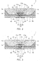
- FIG. 2 is a sectional view taken along line A-A in FIG. 1 .
- the light emitting module 1 includes a light guide plate 10 and a light source 20.
- the light source 20 may include a light emitting element 21, a phosphor layer 22, and a cover member 23.
- the light guide plate 10 transmits the light emitted by the light source 20.
- materials for the light guide plate 10 include a thermoplastic resin such as acrylic, polycarbonate, cyclic polyolefin, polyethylene terephthalate, and polyester, a thermosetting resin such as epoxy and silicone, and glass.
- polycarbonate is preferable due to its highly light transmissivity and inexpensiveness.
- the light guide plate 10 has a first primary face 11, which serves as the emission face, a second primary face 12 opposing the first primary face 11, and a recessed portion 15 created in the second primary face 12. Furthermore, the light guide plate 10 may have lateral faces 13 contiguous with the first primary face 11, and oblique faces 14 between the lateral faces 13 and the second primary face 12.
- At least the phosphor layer 22 of the light source 20 may be disposed in the recessed portion 15 of the light guide plate 10.
- the light emitting element 21 may be disposed on the face of the phosphor layer 22 opposite the face that opposes the first primary face 11 of the light guide plate 10.
- the recessed portion 15 can function as a positioning part for the light source 20 relative to the light guide plate 10.
- the light emitting element 21 has a primary emission face 21b and includes a pair of positive and negative electrodes 21a on the opposite side of the primary emission face 21b.
- the light emitting element 21 has a semiconductor stack structure.
- the semiconductor stack structure includes, for example, In x Al y Ga 1-x-y N (0 ⁇ x, 0 ⁇ y, x+y ⁇ 1) and can emit blue light.
- the primary emission face 21b of the light emitting element 21 may be adhered to the phosphor layer 22 using, for example, a light transmissive adhesive.
- the lateral faces and the electrodes 21a of the light emitting element 21 are positioned outside of the recessed portion 15.
- the light emitting element 21 may be disposed in the recessed portion 15.
- a cover member 23 may be disposed on the lateral faces of the light emitting element 21.
- the cover member 23 may also be disposed between the electrodes 21a at the lower face of the light emitting element 21.
- the cover member 23 reflects the light emitted by the light emitting element 21 and the phosphor in the phosphor layer 22. It is made of, for example, a resin containing a white pigment or the like.
- the cover member 23 is preferably formed of a silicone resin containing titanium oxide.
- the phosphor layer 22 may be made of a base material and a phosphor dispersed in the base material.
- a base material for the phosphor layer 22.
- an epoxy resin, silicone resin, glass, or the like may be used as the base material for the phosphor layer 22. From the light resistance and formability perspectives, a silicone resin is preferably used for the base material.
- the phosphor is excited by the light emitted from the light emitting element 21, and emits light of a different wavelength from that of the light emitted by the light emitting element 21.
- Examples of usable phosphor include YAG phosphors, LAG phosphors, ⁇ -SiAlON phosphors, CASN phosphors, KSF-based phosphors, quantum dot phosphors, and the like.
- the phosphor layer 22 may contain one or more types of phosphors.
- An optical function part 32 may be disposed on the first primary face 11 of the light guide plate 10.
- the optical function part 32 may be disposed in the position facing the recessed portion 15 formed in the second primary face 12.
- the optical axis of the light emitting element 21 and the optical axis of the optical function part 32 preferably coincide with one another.
- the optical function part 32 may have the shape of, for example, an inverted cone, inverted polygonal pyramid such as inverted quadrangular or hexagonal pyramid, inverted frustum, inverted pyramidal frustum, or the like.
- the optical function part 32 may comprise or be a light transmissive resin, glass, or air layer having a lower refractive index than the refractive index of the light guide plate 10, and may function as a lens to diffuse light in the extension direction of the first surface of the light guide plate 10 by refracting the light at the interfaces between the light guide plate 10 and the optical function part 32.
- the light guide plate 10 may alternatively have a configuration in which a light reflecting material (e.g., a metal reflective film or a white resin) is disposed in the recess having oblique faces, for example.
- the recessed portion 15 may have an opening on the second primary face 12, and may have a bottom face 17 located more closely to the first primary face 11 than the second primary face 12.
- a light scattering layer 31 containing a light scattering agent may be disposed on the bottom face 17 of the recessed portion 15.
- the light scattering layer 31 may be disposed between the bottom face 17 of the recessed portion 15 and the phosphor layer 22.
- the light scattering layer 31 may scatter and return downwards a portion of the light emitted straight up from the light emitting element 21. Accordingly, the area and its vicinity directly above the light source 20 in the first primary face 11 of the light guide plate 10, which is the emission face of the light emitting module 1, is less likely to be excessively brighter than the remaining area.
- the light scattering layer 31 may be omitted, in which case the phosphor layer 22 may be disposed directly on the bottom face 17 of the recessed portion 15.
- a light transmitting part 60 may be disposed in the recessed portion 15 and surrounding the light source (specifically, surrounding the phosphor layer 22 and surrounding of the light scattering layer 31).
- the light transmitting part 60 may comprise or may be a light transmissive resin part which transmits the light emitted from the light source 20.
- the refractive index of the light transmissive resin part may be lower than the refractive index of the light guide plate 10.
- the second light transmitting part 60 may be a void or air layer.
- the light guide plate 10 may have oblique faces 14 each forming an obtuse angle and contiguous with the second primary face 12.
- the oblique faces 14 and the second primary face 12 may be covered with a light reflecting resin part 40.
- the light reflecting resin part 40 reflects the light emitted by the light source 20 and is formed of, for example, a resin containing a white pigment or the like. Particularly, the light reflecting resin part 40 is preferably a silicone resin containing titanium oxide.
- the electrodes 21a of the light emitting element 21 are respectively connected to the wirings 52.
- the light reflecting resin part 40 may be an insulator and may cover the lateral faces of the electrodes 21a of the light emitting element 21.
- the light reflecting resin part 40 may be joined to a wiring board 50.
- the wiring board 50 may have an insulating base 51, wirings 54 disposed on the rear surface of the base 51, and vias 53 penetrating the base 51.
- the vias 53 respectively connect the wirings 52 and the wirings 54, and the electrodes 21a of the light emitting element 21 are respectively electrically connected to the wirings 54 through the wirings 52 and the vias 53.
- Examples of materials for the base 51 of the wiring board 50 include a resin and a ceramic material. Examples of materials for the wirings 52 and 54, and the vias 53 include copper.
- a plan view refers to a plan view of the first primary face 11 of the light guide plate 10 as shown in FIG. 1 .
- the first primary face 11 has a polygonal shape with multiple corners 11a, for example, a quadrangular shape or a square shape with four corners 11a.
- the bottom face 17 of the recessed portion 15 may also have a polygonal shape.
- the bottom face 17 of the recessed portion 15 has four long sides 17a and four short sides 17b which are shorter than the long sides 17a.
- the bottom face 17 may have a corner between a long side 17a and a short side 17b.
- the phosphor layer 22 may be polygonal.
- the phosphor layer 22 is, for example, quadrangular or square shaped in a plan view and has four lateral faces 22a.
- the four lateral faces 22a may be each along the long sides 17a of the bottom face 17 of the recessed portion 15.
- the corners of the phosphor layer 22 may be positioned to each face the short sides 17b of the bottom face 17 of the recessed portion 15.
- the diagonal lines connecting opposing corners 11a of the first primary face 11 may intersect with the long sides 17a of the bottom face 17 of the recessed portion 15.
- Position of the phosphor layer 22 on the bottom face 17 of the recessed portion 15 may be determined such that the lateral faces 22a of the phosphor layer 22 are along the long sides 17a of the bottom face 17 of the recessed portion 15.
- the light source 20 having a quadrangular or square shape in a plan view may be positioned so as to be rotated 45 degrees relative to the quadrangular or square-shaped first primary face 11 of the light guide plate 10, for example, to thereby allow the lateral faces 22a of the phosphor layer 22 also serving as the lateral surfaces of the light source 20 (specifically, the sides of the quadrangular or square-shaped phosphor layer 22) to intersect with the diagonal lines connecting opposing corners 11a of the first primary face 11 in a plan view.
- the corners of the light source 20 (specifically, the corners of the phosphor layer 22) may be not positioned on the diagonal lines connecting opposing corners 11a of the first primary face 11, and may be positioned so as not to oppose the corners 11a.
- the corners of the light source 20 (specifically, the corners of the phosphor layer 22) may be positioned in the regions segmented by the diagonal lines connecting opposing corners 11a of the first primary face 11.
- the lateral faces 22a have larger areas than the corners.
- the luminance of the light exiting from the lateral faces 22a of the phosphor layer 22 tends to be higher than the luminance of the light exiting in diagonal directions.
- the distance between the central portion where the phosphor layer 22 is disposed and each corner 11a is larger than the distance between the central portion and each side.
- the light tends not to readily diffuse to the four corners of the first primary face 11.
- positioning the phosphor layer 22 relative to the light guide plate 10 so as to allow the lateral faces 22 of the phosphor layer 22 to intersect with the diagonal lines connecting opposing corners 11a of the first primary face 11 and to face the corners 11a of the first primary face 11 can facilitate the diffusion of the light exiting from the phosphor layer 22 to the four corners of the first primary face 11 of the light guide plate 10. This may reduce luminance non-uniformity and color non-uniformity in the first primary face 11 which is the emission face of the light emitting module 1.
- FIG. 3 is a sectional view taken along line B-B in FIG. 1 .
- FIG. 4 is a perspective view of the constituent elements (e.g., the light scattering layer 31, the phosphor layer 22, and the light transmitting part 60) in the recessed portion 15 of the light guide plate 10 in the light emitting module 1 according to the embodiment.
- the constituent elements e.g., the light scattering layer 31, the phosphor layer 22, and the light transmitting part 60
- the shape of the opening 16 of the recessed portion 15 is, for example, a quadrangular or square, and the shape of the opening 16 of the recessed portion 15 may differ from the shape of the bottom face 17 of the recessed portion 15.
- the recessed portion 15 may have oblique faces 18 each being oblique to, and forming an obtuse angle with, the bottom face 17 of the recessed portion 15.
- the light transmitting part 60 may be in contact with the oblique faces 18 of the recessed portion 15, and may have oblique faces 61 facing the oblique faces 18 of the recessed portion 15.
- the light transmitting part 60 has an upper face 63 in contact with the bottom face 17 of the recessed portion 15 and vertical faces 62 orthogonal to the bottom face 17 of the recessed portion 15.
- the vertical faces 62 may be also in contact with the light guide plate 10.
- Forming the oblique faces 61 in the light transmitting part 60 can increase the area of contact with the light guide plate 10 as compared to the case in which only the upper face 63 and the vertical faces 62 are in contact with the light guide plate 10. In other words, this can increase the interfaces between the different materials, whereby the light exiting from the phosphor layer 22 through the light transmitting part 60 likely to enter into the light guide plate 10.
- the oblique faces 61 are positioned between the corners 11a of the first primary face 11 and the lateral faces 22a of the phosphor layer 22, while facing the corners 11a of the first primary face 11. Accordingly, the light from the phosphor layer 22 can be readily diffused to the four corners of the first primary face 11 of the light guide plate 10 through the oblique faces 61 of the light transmitting part 60, thereby reducing luminance non-uniformity and color non-uniformity in the first primary face 11.
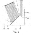
- FIG. 5 is a schematic view of the interfaces between the light guide plate 10 and the light transmitting part 60.
- the refractive index difference between the light transmitting part 60 and the light guide plate 10 by virtue of the oblique faces 61 of the light transmissive part 60 allows the light exiting from the light source 20 to readily advance in the directions of diffusion. Accordingly, the area and its vicinity directly above the light source 20 in the first primary face 11 of the light guide plate 10 is less likely to be excessively brighter than the remaining area, thereby reducing luminance non-uniformity and color non-uniformity. Even in the case where the light transmitting part 60 is configured as a void or air layer, the refractive index difference from that of the light guide plate 10 similarly allows the light exiting from the light source 20 to readily advance in the directions of diffusion.
- FIGS. 6A to 6C are schematic sectional views showing a method of manufacturing the light emitting module 1 according to the embodiment.
- a light guide plate 10 is provided.
- the light guide plate 10 may be formed by, for example, injection molding, transfer molding, thermal transfer, and the like. Forming a recessed portion 19 where an optical function part 32 will be disposed and a recessed portion 15 where a phosphor layer 22 will be disposed all at once using a mold can increase the positioning accuracy between the optical function part 32 and the light emitting element 21.
- a light transmissive resin for example, is supplied in the recessed portion 15.
- the light transmissive resin may be supplied in the recessed portion 15 in a liquid or flowable state by using a method such as potting, printing, spraying, and the like.
- a light source 20 together with a light scattering layer 31 is arranged in the recessed portion 15.
- the light scattering layer 31 may be adhered to the bottom face 17 of the recessed portion 15.
- the light scattering layer 31, the phosphor layer 22, and the light emitting element 21 are supplied in the recessed portion 15 as one unit in the state of being bonded with one another.
- the phosphor layer 22 which is quadrangular or square-shaped in a plan view is positioned in a self-aligned manner such that the lateral faces 22a are along the long sides 17a of the bottom face 17 of the recessed portion 15. Accordingly, the light emitting element 21 is also positioned relative to the light guide plate 10 in a self-aligned manner. Because the area of the opening 16 of the recessed portion 15 is larger than the area of the bottom face 17, the light scattering layer 31 and the phosphor layer 22 can be easily disposed in the recessed portion 15.
- the optical function part 32 shown in FIG. 2 may be provided in the recessed portion 19 on the first primary face 11 side of the light guide plate 10, and a light reflecting resin part 40 may be disposed to cover the oblique faces 14 and the second primary face 12 of the light guide plate 10.
- a wiring board 50 may be adhered below the light reflecting resin part 40.
- the distance between the light guide plate 10 and the light emitting element 21 can be reduced. This can reduce the thickness of the light emitting module 1.
- a light emitting module 1 can be used, for example, as a backlight for a liquid crystal display.
- the distance between the liquid crystal panel and the light emitting module 1 is short in, for example, a direct-lit liquid crystal display in which the backlight is installed on the rear surface of the liquid crystal panel. Therefore, the luminance and color non-uniformities in the light emitting module 1 readily affect the luminance and color non-uniformities of the liquid crystal display.
- Using such a light emitting module 1 having reduced luminance and color non-uniformities according to the embodiment as the backlight of a direct-lit liquid crystal display can contribute to reduction of the luminance and color non-uniformities of the liquid crystal display.
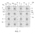
- FIG. 7 is a schematic top view of a light emitting module 100 according to another embodiment of the present disclosure.
- the light emitting module 100 has a single light guide plate 10, and a plurality of cells 2 periodically arranged on the light guide plate 10. Each cell 2 has the same structure as that of the light emitting module 1 described above.
- the light guide plate 10 is provided with a plurality of optical function parts 32 on the first primary face 11 side and a plurality of recessed portions 15 on the second primary face 12 side.
- a light scattering layer 31 In each recessed portion 15, a light scattering layer 31, a light source 20, and a light transmitting part 60 are disposed.
- FIG. 7 is a plan view of the first primary face 11 of the light guide plate 10.
- each cell 2 is formed to have a quadrangular or square shape having four corners 2a, for example.
- Each cell 2 may be arranged such that its sides are along the sides of the first primary face 11 of the light guide plate 10.
- the long sides 17a of the bottom face 17 of the recessed portion 15 and the lateral faces of the light sources 20 may respectively face the corners 2a in each cell 2.
- the diagonal lines connecting opposing corners 2a may intersect with the long sides 17a of the bottom face 17 of the recessed portion 15 in each cell 2.
- the diagonal lines connecting opposing corners 2a in a cell 2 may intersect with the lateral faces 22a of the phosphor layer 22 in the cell 2.
- the light exiting from the phosphor layer 22 in each cell 2 can readily diffuse to the four corners of the cell 2.
- the luminance non-uniformity and color non-uniformity in the emission face of the light emitting module 100 can be reduced.
Landscapes
- Physics & Mathematics (AREA)
- Nonlinear Science (AREA)
- General Physics & Mathematics (AREA)
- Optics & Photonics (AREA)
- Mathematical Physics (AREA)
- Chemical & Material Sciences (AREA)
- Crystallography & Structural Chemistry (AREA)
- Engineering & Computer Science (AREA)
- Microelectronics & Electronic Packaging (AREA)
- Planar Illumination Modules (AREA)
Abstract
Description
- This application claims priority to Japanese Patent Application No.
2019-120060 filed on June 27, 2019 2020-064515 filed on March 31, 2020 - The present disclosure relates to a light emitting module.
- Light emitting modules employing light emitting elements such as light emitting diodes are widely utilized as planar light sources, for example, backlights for liquid crystal displays. For example, in direct-lit liquid crystal displays in which planar light sources are installed on the rear surfaces of the liquid crystal panels, there is an increasing demand for thinner planar light sources. In a configuration in which the distance between the light source and the emission face of a light guide plate is short as the planar light source becomes thinner, light is not fully diffused which tends to cause luminance non-uniformity and color non-uniformity to occur in the emission face. See, for example, Japanese Patent Publication No.
2018-133304 - One of the objects of the present disclosure is to provide a light emitting module in which luminance non-uniformity and color non-uniformity in the emission face of the light guide plate may be reduced.
- A light emitting module according to certain embodiment of the present disclosure includes a light guide plate and a light source. The light guide plate has a polygonal shape with a plurality of corners in a plan view. The light guide plate has a first primary face which serves as an emission face, a second primary face opposing the first primary face, and a recessed portion in the second primary face. The light source is disposed in the recessed portion. The recessed portion defines an opening on the second primary face, and a bottom face having a polygonal shape in a plan view. The light source has lateral faces along sides of the bottom face of the recessed portion. In a plan view, diagonal lines connecting opposing corners of the first primary face intersect with the sides of the bottom face of the recessed portion.
- In accordance with the present disclosure, a light emitting module in which luminance non-uniformity and color non-uniformity in the emission face of the light guide plate may be reduced.
-
-
FIG. 1 is a schematic top view of a light emitting module according to an embodiment of the present disclosure. -
FIG. 2 is a sectional view taken along line A-A inFIG. 1 . -
FIG. 3 is a sectional view taken along line B-B inFIG. 1 . -
FIG. 4 is a perspective view of the elements in the recessed portion of the light guide plate in the light emitting module according to the embodiment. -
FIG. 5 is a schematic view of the interfaces between the light guide plate and the light transmitting part in the light emitting module according to the embodiment. -
FIG. 6A is a schematic sectional view showing a method of manufacturing a light emitting module according to the embodiment. -
FIG. 6B is a schematic sectional view showing a method of manufacturing a light emitting module according to the embodiment. -
FIG. 6C is a schematic sectional view showing a method of manufacturing a light emitting module according to the embodiment. -
FIG. 7 is a schematic top view of a light emitting module according to another embodiment of the present disclosure. - Certain embodiments of the present disclosure will be explained below with reference to the accompanying drawings. In the drawings, the same elements are denoted with the same reference numerals.
-
FIG. 1 is a schematic top view of alight emitting module 1 according to an embodiment of the present disclosure.FIG. 2 is a sectional view taken along line A-A inFIG. 1 . - The
light emitting module 1 includes alight guide plate 10 and alight source 20. Thelight source 20 may include alight emitting element 21, aphosphor layer 22, and acover member 23. - The
light guide plate 10 transmits the light emitted by thelight source 20. Examples of materials for thelight guide plate 10 include a thermoplastic resin such as acrylic, polycarbonate, cyclic polyolefin, polyethylene terephthalate, and polyester, a thermosetting resin such as epoxy and silicone, and glass. Among these examples, polycarbonate is preferable due to its highly light transmissivity and inexpensiveness. - The
light guide plate 10 has a firstprimary face 11, which serves as the emission face, a secondprimary face 12 opposing the firstprimary face 11, and arecessed portion 15 created in the secondprimary face 12. Furthermore, thelight guide plate 10 may havelateral faces 13 contiguous with the firstprimary face 11, andoblique faces 14 between thelateral faces 13 and the secondprimary face 12. - At least the
phosphor layer 22 of thelight source 20 may be disposed in therecessed portion 15 of thelight guide plate 10. Thelight emitting element 21 may be disposed on the face of thephosphor layer 22 opposite the face that opposes the firstprimary face 11 of thelight guide plate 10. Therecessed portion 15 can function as a positioning part for thelight source 20 relative to thelight guide plate 10. - The
light emitting element 21 has aprimary emission face 21b and includes a pair of positive andnegative electrodes 21a on the opposite side of theprimary emission face 21b. Thelight emitting element 21 has a semiconductor stack structure. The semiconductor stack structure includes, for example, InxAlyGa1-x-yN (0≤x, 0≤y, x+y≤1) and can emit blue light. - The primary emission face 21b of the
light emitting element 21 may be adhered to thephosphor layer 22 using, for example, a light transmissive adhesive. In the example shown inFIG. 2 and FIG. 3 , the lateral faces and theelectrodes 21a of thelight emitting element 21 are positioned outside of the recessedportion 15. Alternatively, thelight emitting element 21 may be disposed in therecessed portion 15. Acover member 23 may be disposed on the lateral faces of thelight emitting element 21. Thecover member 23 may also be disposed between theelectrodes 21a at the lower face of thelight emitting element 21. Thecover member 23 reflects the light emitted by thelight emitting element 21 and the phosphor in thephosphor layer 22. It is made of, for example, a resin containing a white pigment or the like. Particularly, thecover member 23 is preferably formed of a silicone resin containing titanium oxide. - The
phosphor layer 22 may be made of a base material and a phosphor dispersed in the base material. For example, an epoxy resin, silicone resin, glass, or the like may be used as the base material for thephosphor layer 22. From the light resistance and formability perspectives, a silicone resin is preferably used for the base material. - The phosphor is excited by the light emitted from the
light emitting element 21, and emits light of a different wavelength from that of the light emitted by thelight emitting element 21. Examples of usable phosphor include YAG phosphors, LAG phosphors, β-SiAlON phosphors, CASN phosphors, KSF-based phosphors, quantum dot phosphors, and the like. Thephosphor layer 22 may contain one or more types of phosphors. - An
optical function part 32 may be disposed on the firstprimary face 11 of thelight guide plate 10. Theoptical function part 32 may be disposed in the position facing therecessed portion 15 formed in the secondprimary face 12. The optical axis of thelight emitting element 21 and the optical axis of theoptical function part 32 preferably coincide with one another. Theoptical function part 32 may have the shape of, for example, an inverted cone, inverted polygonal pyramid such as inverted quadrangular or hexagonal pyramid, inverted frustum, inverted pyramidal frustum, or the like. - The
optical function part 32 may comprise or be a light transmissive resin, glass, or air layer having a lower refractive index than the refractive index of thelight guide plate 10, and may function as a lens to diffuse light in the extension direction of the first surface of thelight guide plate 10 by refracting the light at the interfaces between thelight guide plate 10 and theoptical function part 32. Thelight guide plate 10 may alternatively have a configuration in which a light reflecting material (e.g., a metal reflective film or a white resin) is disposed in the recess having oblique faces, for example. - The recessed
portion 15 may have an opening on the secondprimary face 12, and may have abottom face 17 located more closely to the firstprimary face 11 than the secondprimary face 12. Alight scattering layer 31 containing a light scattering agent may be disposed on thebottom face 17 of the recessedportion 15. Thelight scattering layer 31 may be disposed between thebottom face 17 of the recessedportion 15 and thephosphor layer 22. Thelight scattering layer 31 may scatter and return downwards a portion of the light emitted straight up from thelight emitting element 21. Accordingly, the area and its vicinity directly above thelight source 20 in the firstprimary face 11 of thelight guide plate 10, which is the emission face of thelight emitting module 1, is less likely to be excessively brighter than the remaining area. Thelight scattering layer 31 may be omitted, in which case thephosphor layer 22 may be disposed directly on thebottom face 17 of the recessedportion 15. - A
light transmitting part 60 may be disposed in the recessedportion 15 and surrounding the light source (specifically, surrounding thephosphor layer 22 and surrounding of the light scattering layer 31). Thelight transmitting part 60 may comprise or may be a light transmissive resin part which transmits the light emitted from thelight source 20. The refractive index of the light transmissive resin part may be lower than the refractive index of thelight guide plate 10. The secondlight transmitting part 60 may be a void or air layer. - The
light guide plate 10 may have oblique faces 14 each forming an obtuse angle and contiguous with the secondprimary face 12. The oblique faces 14 and the secondprimary face 12 may be covered with a light reflectingresin part 40. - The light reflecting
resin part 40 reflects the light emitted by thelight source 20 and is formed of, for example, a resin containing a white pigment or the like. Particularly, the light reflectingresin part 40 is preferably a silicone resin containing titanium oxide. - The
electrodes 21a of thelight emitting element 21 are respectively connected to thewirings 52. The light reflectingresin part 40 may be an insulator and may cover the lateral faces of theelectrodes 21a of thelight emitting element 21. - The light reflecting
resin part 40 may be joined to awiring board 50. Thewiring board 50 may have an insulatingbase 51, wirings 54 disposed on the rear surface of thebase 51, and vias 53 penetrating thebase 51. Thevias 53 respectively connect thewirings 52 and thewirings 54, and theelectrodes 21a of thelight emitting element 21 are respectively electrically connected to thewirings 54 through thewirings 52 and thevias 53. - Examples of materials for the
base 51 of thewiring board 50 include a resin and a ceramic material. Examples of materials for thewirings vias 53 include copper. - In the description herein, a plan view refers to a plan view of the first
primary face 11 of thelight guide plate 10 as shown inFIG. 1 . In such a plan view, the firstprimary face 11 has a polygonal shape withmultiple corners 11a, for example, a quadrangular shape or a square shape with fourcorners 11a. - In a plan view, the
bottom face 17 of the recessedportion 15 may also have a polygonal shape. For example, thebottom face 17 of the recessedportion 15 has fourlong sides 17a and fourshort sides 17b which are shorter than thelong sides 17a. Furthermore, thebottom face 17 may have a corner between along side 17a and ashort side 17b. - In a plan view, the
phosphor layer 22 may be polygonal. Thephosphor layer 22 is, for example, quadrangular or square shaped in a plan view and has fourlateral faces 22a. The fourlateral faces 22a may be each along thelong sides 17a of thebottom face 17 of the recessedportion 15. In a plan view, the corners of thephosphor layer 22 may be positioned to each face theshort sides 17b of thebottom face 17 of the recessedportion 15. - In a plan view, the diagonal lines connecting opposing
corners 11a of the firstprimary face 11 may intersect with thelong sides 17a of thebottom face 17 of the recessedportion 15. Position of thephosphor layer 22 on thebottom face 17 of the recessedportion 15 may be determined such that the lateral faces 22a of thephosphor layer 22 are along thelong sides 17a of thebottom face 17 of the recessedportion 15. - The
light source 20 having a quadrangular or square shape in a plan view may be positioned so as to be rotated 45 degrees relative to the quadrangular or square-shaped firstprimary face 11 of thelight guide plate 10, for example, to thereby allow the lateral faces 22a of thephosphor layer 22 also serving as the lateral surfaces of the light source 20 (specifically, the sides of the quadrangular or square-shaped phosphor layer 22) to intersect with the diagonal lines connecting opposingcorners 11a of the firstprimary face 11 in a plan view. In a plan view, the corners of the light source 20 (specifically, the corners of the phosphor layer 22) may be not positioned on the diagonal lines connecting opposingcorners 11a of the firstprimary face 11, and may be positioned so as not to oppose thecorners 11a. In a plan view, the corners of the light source 20 (specifically, the corners of the phosphor layer 22) may be positioned in the regions segmented by the diagonal lines connecting opposingcorners 11a of the firstprimary face 11. - In the
phosphor layer 22, the lateral faces 22a have larger areas than the corners. Thus, the luminance of the light exiting from the lateral faces 22a of thephosphor layer 22 tends to be higher than the luminance of the light exiting in diagonal directions. - In the quadrangular or square-shaped first
primary face 11 of thelight guide plate 10, moreover, the distance between the central portion where thephosphor layer 22 is disposed and eachcorner 11a is larger than the distance between the central portion and each side. Thus, the light tends not to readily diffuse to the four corners of the firstprimary face 11. - In accordance with the embodiment of the present disclosure, positioning the
phosphor layer 22 relative to thelight guide plate 10 so as to allow the lateral faces 22 of thephosphor layer 22 to intersect with the diagonal lines connecting opposingcorners 11a of the firstprimary face 11 and to face thecorners 11a of the firstprimary face 11 can facilitate the diffusion of the light exiting from thephosphor layer 22 to the four corners of the firstprimary face 11 of thelight guide plate 10. This may reduce luminance non-uniformity and color non-uniformity in the firstprimary face 11 which is the emission face of thelight emitting module 1. -
FIG. 3 is a sectional view taken along line B-B inFIG. 1 .FIG. 4 is a perspective view of the constituent elements (e.g., thelight scattering layer 31, thephosphor layer 22, and the light transmitting part 60) in the recessedportion 15 of thelight guide plate 10 in thelight emitting module 1 according to the embodiment. - The shape of the
opening 16 of the recessedportion 15 is, for example, a quadrangular or square, and the shape of theopening 16 of the recessedportion 15 may differ from the shape of thebottom face 17 of the recessedportion 15. - The recessed
portion 15 may have oblique faces 18 each being oblique to, and forming an obtuse angle with, thebottom face 17 of the recessedportion 15. Thelight transmitting part 60 may be in contact with the oblique faces 18 of the recessedportion 15, and may have oblique faces 61 facing the oblique faces 18 of the recessedportion 15. - As shown in
FIG. 2 andFIG. 4 , thelight transmitting part 60 has anupper face 63 in contact with thebottom face 17 of the recessedportion 15 andvertical faces 62 orthogonal to thebottom face 17 of the recessedportion 15. The vertical faces 62 may be also in contact with thelight guide plate 10. - Forming the oblique faces 61 in the
light transmitting part 60 can increase the area of contact with thelight guide plate 10 as compared to the case in which only theupper face 63 and the vertical faces 62 are in contact with thelight guide plate 10. In other words, this can increase the interfaces between the different materials, whereby the light exiting from thephosphor layer 22 through thelight transmitting part 60 likely to enter into thelight guide plate 10. - In the plan view in
FIG. 1 , the oblique faces 61 are positioned between thecorners 11a of the firstprimary face 11 and the lateral faces 22a of thephosphor layer 22, while facing thecorners 11a of the firstprimary face 11. Accordingly, the light from thephosphor layer 22 can be readily diffused to the four corners of the firstprimary face 11 of thelight guide plate 10 through the oblique faces 61 of thelight transmitting part 60, thereby reducing luminance non-uniformity and color non-uniformity in the firstprimary face 11. -
FIG. 5 is a schematic view of the interfaces between thelight guide plate 10 and thelight transmitting part 60. - The refractive index difference between the light transmitting
part 60 and thelight guide plate 10 by virtue of the oblique faces 61 of thelight transmissive part 60 allows the light exiting from thelight source 20 to readily advance in the directions of diffusion. Accordingly, the area and its vicinity directly above thelight source 20 in the firstprimary face 11 of thelight guide plate 10 is less likely to be excessively brighter than the remaining area, thereby reducing luminance non-uniformity and color non-uniformity. Even in the case where thelight transmitting part 60 is configured as a void or air layer, the refractive index difference from that of thelight guide plate 10 similarly allows the light exiting from thelight source 20 to readily advance in the directions of diffusion. -
FIGS. 6A to 6C are schematic sectional views showing a method of manufacturing thelight emitting module 1 according to the embodiment. - As shown in
FIG. 6A , alight guide plate 10 is provided. Thelight guide plate 10 may be formed by, for example, injection molding, transfer molding, thermal transfer, and the like. Forming a recessedportion 19 where anoptical function part 32 will be disposed and a recessedportion 15 where aphosphor layer 22 will be disposed all at once using a mold can increase the positioning accuracy between theoptical function part 32 and thelight emitting element 21. - As shown in
FIG. 6B , for thelight transmitting part 60, a light transmissive resin, for example, is supplied in the recessedportion 15. The light transmissive resin may be supplied in the recessedportion 15 in a liquid or flowable state by using a method such as potting, printing, spraying, and the like. - After supplying the
light transmitting part 50 to the recessedportion 15, as shown inFIG. 6C , alight source 20 together with alight scattering layer 31 is arranged in the recessedportion 15. Thelight scattering layer 31 may be adhered to thebottom face 17 of the recessedportion 15. - The
light scattering layer 31, thephosphor layer 22, and thelight emitting element 21 are supplied in the recessedportion 15 as one unit in the state of being bonded with one another. At this point, thephosphor layer 22 which is quadrangular or square-shaped in a plan view is positioned in a self-aligned manner such that the lateral faces 22a are along thelong sides 17a of thebottom face 17 of the recessedportion 15. Accordingly, thelight emitting element 21 is also positioned relative to thelight guide plate 10 in a self-aligned manner. Because the area of theopening 16 of the recessedportion 15 is larger than the area of thebottom face 17, thelight scattering layer 31 and thephosphor layer 22 can be easily disposed in the recessedportion 15. - Subsequently, the
optical function part 32 shown inFIG. 2 may be provided in the recessedportion 19 on the firstprimary face 11 side of thelight guide plate 10, and a light reflectingresin part 40 may be disposed to cover the oblique faces 14 and the secondprimary face 12 of thelight guide plate 10. Awiring board 50 may be adhered below the light reflectingresin part 40. - In the
light emitting module 1 according to the embodiment, because thelight emitting element 21 is mounted on thelight guide plate 10, but not on thewiring board 50, the distance between thelight guide plate 10 and thelight emitting element 21 can be reduced. This can reduce the thickness of thelight emitting module 1. Such alight emitting module 1 can be used, for example, as a backlight for a liquid crystal display. The distance between the liquid crystal panel and thelight emitting module 1 is short in, for example, a direct-lit liquid crystal display in which the backlight is installed on the rear surface of the liquid crystal panel. Therefore, the luminance and color non-uniformities in thelight emitting module 1 readily affect the luminance and color non-uniformities of the liquid crystal display. Using such alight emitting module 1 having reduced luminance and color non-uniformities according to the embodiment as the backlight of a direct-lit liquid crystal display can contribute to reduction of the luminance and color non-uniformities of the liquid crystal display. -
FIG. 7 is a schematic top view of alight emitting module 100 according to another embodiment of the present disclosure. - The
light emitting module 100 has a singlelight guide plate 10, and a plurality ofcells 2 periodically arranged on thelight guide plate 10. Eachcell 2 has the same structure as that of thelight emitting module 1 described above. - In other words, the
light guide plate 10 is provided with a plurality ofoptical function parts 32 on the firstprimary face 11 side and a plurality of recessedportions 15 on the secondprimary face 12 side. In each recessedportion 15, alight scattering layer 31, alight source 20, and alight transmitting part 60 are disposed. -
FIG. 7 is a plan view of the firstprimary face 11 of thelight guide plate 10. In the plan view, eachcell 2 is formed to have a quadrangular or square shape having fourcorners 2a, for example. Eachcell 2 may be arranged such that its sides are along the sides of the firstprimary face 11 of thelight guide plate 10. In a plan view, thelong sides 17a of thebottom face 17 of the recessedportion 15 and the lateral faces of the light sources 20 (specifically, the lateral faces 22a of the phosphor layer 22) may respectively face thecorners 2a in eachcell 2. The diagonal lines connecting opposingcorners 2a may intersect with thelong sides 17a of thebottom face 17 of the recessedportion 15 in eachcell 2. The diagonal lines connecting opposingcorners 2a in acell 2 may intersect with the lateral faces 22a of thephosphor layer 22 in thecell 2. - Accordingly, the light exiting from the
phosphor layer 22 in eachcell 2 can readily diffuse to the four corners of thecell 2. By inhibiting the luminance from concentrating in the center in eachcell 2 across the entire firstprimary face 11, which is the emission face of thelight emitting module 100, the luminance non-uniformity and color non-uniformity in the emission face of thelight emitting module 100 can be reduced. - In the foregoing, certain embodiments of the present disclosure have been explained with reference to specific examples. The present disclosure, however, is not limited to these specific examples. All forms implementable by a person skilled in the art by suitably making design changes based on any of the embodiments disclosed above also fall within the scope of the present invention so long as they encompass the subject matter of the present disclosure. Furthermore, various modifications and alterations within the spirit of the present disclosure that could have been made by a person skilled in the art are also considered as those falling within the scope of the present disclosure.
Claims (10)
- A light emitting module comprising:a light guide plate having a polygonal shape with a plurality of corners in a plan view, the light guide plate having a first primary face which serves as an emission face, a second primary face opposing the first primary face, and a recessed portion in the second primary face,a light source disposed in the recessed portion, whereinthe recessed portion has an opening on the second primary face, and a bottom face having a polygonal shape in a plan view,the light source has lateral faces along sides of the bottom face of the recessed portion, andin a plan view, diagonal lines connecting opposing corners of the first primary face intersect with the sides of the bottom face of the recessed portion.
- The light emitting module according to claim 1, wherein the diagonal lines connecting opposing corners of the first primary face intersect with lateral faces of a phosphor layer.
- The light emitting module according to any of the preceding claims, comprising:a plurality of cells each having a quadrangular shape and a recessed portion, each including a light source, the cells periodically arranged on the light guide plate,in a plan view, in each of the plurality of cells, the sides of the bottom face of the recessed portion and the lateral faces of the light source respectively face corners of the cell.
- The light emitting module according to any of the preceding claims, wherein the recessed portion has an oblique face being oblique to the bottom face of the recessed portion, and forming an obtuse angle with the bottom face of the recessed portion.
- The light emitting module according to claim 4 further comprising a light transmitting part disposed in the recessed portion and surrounding the light source.
- The light emitting module according to claim 5, wherein the light transmitting part comprises a light transmissive resin part.
- The light emitting module according to claim 6, wherein a refractive index of the light transmissive resin part is lower than a refractive index of the light guide plate.
- The light emitting module according to any of the preceding claims, wherein an area of the opening of the recessed portion is larger than an area of the bottom face of the recessed portion.
- The light emitting module according to any of the preceding claims, further comprising, an optical function part disposed in the first primary face of the light guide plate in a position to face the recessed portion, and having a lower refractive index than a refractive index of the light guide plate.
- The light emitting module according to any of the preceding claims, wherein the light source includes a light emitting element and a phosphor layer adhered to a primary emission face of the light emitting element.
Applications Claiming Priority (2)
| Application Number | Priority Date | Filing Date | Title |
|---|---|---|---|
| JP2019120060 | 2019-06-27 | ||
| JP2020064515A JP6909987B2 (en) | 2019-06-27 | 2020-03-31 | Luminous module |
Publications (2)
| Publication Number | Publication Date |
|---|---|
| EP3757454A1 true EP3757454A1 (en) | 2020-12-30 |
| EP3757454B1 EP3757454B1 (en) | 2022-11-30 |
Family
ID=71143546
Family Applications (1)
| Application Number | Title | Priority Date | Filing Date |
|---|---|---|---|
| EP20182003.2A Active EP3757454B1 (en) | 2019-06-27 | 2020-06-24 | Light emitting module |
Country Status (4)
| Country | Link |
|---|---|
| US (2) | US11036083B2 (en) |
| EP (1) | EP3757454B1 (en) |
| KR (1) | KR20210001964A (en) |
| CN (1) | CN112151655B (en) |
Families Citing this family (3)
| Publication number | Priority date | Publication date | Assignee | Title |
|---|---|---|---|---|
| KR20210001964A (en) | 2019-06-27 | 2021-01-06 | 니치아 카가쿠 고교 가부시키가이샤 | Light emitting module |
| JP2024070729A (en) * | 2022-11-11 | 2024-05-23 | 日亜化学工業株式会社 | Surface Light Source |
| TWI861954B (en) * | 2023-06-21 | 2024-11-11 | 達運精密工業股份有限公司 | Backlight module |
Citations (8)
| Publication number | Priority date | Publication date | Assignee | Title |
|---|---|---|---|---|
| US20060002146A1 (en) * | 2004-07-01 | 2006-01-05 | Nec Lcd Technologies, Ltd. | Backlight unit and liquid crystal display device using the same |
| JP2007180021A (en) * | 2005-11-30 | 2007-07-12 | Showa Denko Kk | Light guide member, surface light source device including the light guide member, and display device using the surface light source device |
| US20090086508A1 (en) * | 2007-09-27 | 2009-04-02 | Philips Lumileds Lighting Company, Llc | Thin Backlight Using Low Profile Side Emitting LEDs |
| US20100220484A1 (en) * | 2008-07-10 | 2010-09-02 | Oree Inc. | Slim waveguide coupling apparatus and method |
| EP2420723A1 (en) * | 2009-04-14 | 2012-02-22 | Sharp Kabushiki Kaisha | Planar light source device and display device provided with the planar light source device |
| US20120140464A1 (en) * | 2010-12-07 | 2012-06-07 | Industrial Technology Research Institute | Flexible light source module |
| JP2018133304A (en) | 2017-02-17 | 2018-08-23 | 日亜化学工業株式会社 | Light emitting module manufacturing method and light emitting module |
| EP3579273A1 (en) * | 2018-06-04 | 2019-12-11 | Nichia Corporation | Light-emitting device and surface-emitting light source |
Family Cites Families (21)
| Publication number | Priority date | Publication date | Assignee | Title |
|---|---|---|---|---|
| JP3688832B2 (en) * | 1996-12-13 | 2005-08-31 | ローム株式会社 | Linear light source device, light guide member used therefor, and image reading device including a linear light source using the light guide member |
| US7997771B2 (en) | 2004-06-01 | 2011-08-16 | 3M Innovative Properties Company | LED array systems |
| CN100470853C (en) * | 2004-09-17 | 2009-03-18 | 清华大学 | Collimated light-emitting diode packaging structure |
| JP4600257B2 (en) | 2005-11-25 | 2010-12-15 | ソニー株式会社 | Light guide plate, backlight device, manufacturing method thereof, and liquid crystal display device |
| KR20090117419A (en) | 2008-05-09 | 2009-11-12 | 엘지이노텍 주식회사 | Display |
| US20110037740A1 (en) | 2008-12-15 | 2011-02-17 | Panasonic Corporation | Planar illumination device and liquid crystal display |
| JP2010212083A (en) | 2009-03-10 | 2010-09-24 | Sharp Corp | Light source unit, lighting system, and liquid crystal display device |
| JP5568263B2 (en) | 2009-08-06 | 2014-08-06 | 株式会社ジャパンディスプレイ | Liquid crystal display |
| CN201672381U (en) * | 2010-05-07 | 2010-12-15 | 深圳市晶鼎源光电科技有限公司 | LED backlight source |
| TWI529459B (en) | 2010-06-15 | 2016-04-11 | Lg伊諾特股份有限公司 | The backlight unit and the desplay device having the same |
| WO2012132872A1 (en) | 2011-03-25 | 2012-10-04 | ナルックス株式会社 | Illumination device |
| TWI582349B (en) * | 2013-10-28 | 2017-05-11 | 鴻海精密工業股份有限公司 | Composite lens and light source device using the same |
| US20190249004A1 (en) | 2016-10-18 | 2019-08-15 | Bromine Compounds Ltd. | Flame-retarded polyester compositions |
| JP6827635B2 (en) | 2016-12-09 | 2021-02-10 | 日亜化学工業株式会社 | Surface light source device, display device and electronic equipment |
| JP6857297B2 (en) | 2016-12-22 | 2021-04-14 | 日亜化学工業株式会社 | Light guide plate, surface light source device, display device and electronic device |
| JP6766795B2 (en) | 2017-06-30 | 2020-10-14 | 日亜化学工業株式会社 | Light emitting module manufacturing method and light emitting module |
| JP6879325B2 (en) | 2018-03-26 | 2021-06-02 | 日亜化学工業株式会社 | Light emitting module manufacturing method and light emitting module |
| JP6669217B2 (en) * | 2018-08-30 | 2020-03-18 | 日亜化学工業株式会社 | Package and light emitting device using the same |
| JP6841292B2 (en) * | 2019-03-05 | 2021-03-10 | 日亜化学工業株式会社 | Luminous module |
| KR20210001964A (en) | 2019-06-27 | 2021-01-06 | 니치아 카가쿠 고교 가부시키가이샤 | Light emitting module |
| JP6909987B2 (en) * | 2019-06-27 | 2021-07-28 | 日亜化学工業株式会社 | Luminous module |
-
2020
- 2020-06-18 KR KR1020200074207A patent/KR20210001964A/en not_active Ceased
- 2020-06-24 EP EP20182003.2A patent/EP3757454B1/en active Active
- 2020-06-24 CN CN202010587438.XA patent/CN112151655B/en active Active
- 2020-06-25 US US16/911,922 patent/US11036083B2/en active Active
-
2021
- 2021-05-03 US US17/302,459 patent/US11402691B2/en active Active
Patent Citations (8)
| Publication number | Priority date | Publication date | Assignee | Title |
|---|---|---|---|---|
| US20060002146A1 (en) * | 2004-07-01 | 2006-01-05 | Nec Lcd Technologies, Ltd. | Backlight unit and liquid crystal display device using the same |
| JP2007180021A (en) * | 2005-11-30 | 2007-07-12 | Showa Denko Kk | Light guide member, surface light source device including the light guide member, and display device using the surface light source device |
| US20090086508A1 (en) * | 2007-09-27 | 2009-04-02 | Philips Lumileds Lighting Company, Llc | Thin Backlight Using Low Profile Side Emitting LEDs |
| US20100220484A1 (en) * | 2008-07-10 | 2010-09-02 | Oree Inc. | Slim waveguide coupling apparatus and method |
| EP2420723A1 (en) * | 2009-04-14 | 2012-02-22 | Sharp Kabushiki Kaisha | Planar light source device and display device provided with the planar light source device |
| US20120140464A1 (en) * | 2010-12-07 | 2012-06-07 | Industrial Technology Research Institute | Flexible light source module |
| JP2018133304A (en) | 2017-02-17 | 2018-08-23 | 日亜化学工業株式会社 | Light emitting module manufacturing method and light emitting module |
| EP3579273A1 (en) * | 2018-06-04 | 2019-12-11 | Nichia Corporation | Light-emitting device and surface-emitting light source |
Also Published As
| Publication number | Publication date |
|---|---|
| CN112151655A (en) | 2020-12-29 |
| US11036083B2 (en) | 2021-06-15 |
| US20200409220A1 (en) | 2020-12-31 |
| EP3757454B1 (en) | 2022-11-30 |
| US11402691B2 (en) | 2022-08-02 |
| KR20210001964A (en) | 2021-01-06 |
| US20210255508A1 (en) | 2021-08-19 |
| CN112151655B (en) | 2025-04-18 |
Similar Documents
| Publication | Publication Date | Title |
|---|---|---|
| US12050338B2 (en) | Light emitting module and method of manufacturing same | |
| US11150508B2 (en) | Light emitting device | |
| US10884290B2 (en) | Light emittng module | |
| JP7236630B2 (en) | light emitting module | |
| KR102681540B1 (en) | Planar light source | |
| JP6703312B2 (en) | Light emitting module and surface emitting light source | |
| US11402691B2 (en) | Light source and light plate for light emitting module | |
| US11035994B2 (en) | Light-emitting module | |
| JP6680311B2 (en) | Light emitting device and surface emitting light source | |
| EP3705773B1 (en) | Light emitting module | |
| US11719975B2 (en) | Light-emitting module and surface-emitting light source | |
| CN115128865B (en) | Reflective component and light source device | |
| TW202020362A (en) | Light emitting device | |
| US11391878B2 (en) | Light emitting module | |
| US11029561B2 (en) | Light emitting module and planar light source | |
| CN213093218U (en) | Light emitting module | |
| CN116893532A (en) | Planar light source and liquid crystal display device | |
| TW202300817A (en) | Partitioning member and planar light source | |
| KR101824035B1 (en) | backlight unit and display apparatus using the same | |
| US20250102725A1 (en) | Optical module | |
| KR20130046732A (en) | Backlight unit and illumination system using the same |
Legal Events
| Date | Code | Title | Description |
|---|---|---|---|
| PUAI | Public reference made under article 153(3) epc to a published international application that has entered the european phase |
Free format text: ORIGINAL CODE: 0009012 |
|
| STAA | Information on the status of an ep patent application or granted ep patent |
Free format text: STATUS: THE APPLICATION HAS BEEN PUBLISHED |
|
| AK | Designated contracting states |
Kind code of ref document: A1 Designated state(s): AL AT BE BG CH CY CZ DE DK EE ES FI FR GB GR HR HU IE IS IT LI LT LU LV MC MK MT NL NO PL PT RO RS SE SI SK SM TR |
|
| AX | Request for extension of the european patent |
Extension state: BA ME |
|
| STAA | Information on the status of an ep patent application or granted ep patent |
Free format text: STATUS: REQUEST FOR EXAMINATION WAS MADE |
|
| STAA | Information on the status of an ep patent application or granted ep patent |
Free format text: STATUS: EXAMINATION IS IN PROGRESS |
|
| 17P | Request for examination filed |
Effective date: 20210520 |
|
| RBV | Designated contracting states (corrected) |
Designated state(s): AL AT BE BG CH CY CZ DE DK EE ES FI FR GB GR HR HU IE IS IT LI LT LU LV MC MK MT NL NO PL PT RO RS SE SI SK SM TR |
|
| 17Q | First examination report despatched |
Effective date: 20210617 |
|
| RIC1 | Information provided on ipc code assigned before grant |
Ipc: H01L 25/075 20060101ALN20211117BHEP Ipc: H01L 33/60 20100101ALN20211117BHEP Ipc: H01L 33/58 20100101ALN20211117BHEP Ipc: H01L 33/50 20100101ALN20211117BHEP Ipc: H01L 33/48 20100101ALN20211117BHEP Ipc: F21V 7/00 20060101ALI20211117BHEP Ipc: F21V 5/00 20180101ALI20211117BHEP Ipc: F21K 9/61 20160101ALI20211117BHEP Ipc: G02B 6/00 20060101ALI20211117BHEP Ipc: G02F 1/13357 20060101ALI20211117BHEP Ipc: G02F 1/1335 20060101ALI20211117BHEP Ipc: F21V 8/00 20060101AFI20211117BHEP |
|
| GRAP | Despatch of communication of intention to grant a patent |
Free format text: ORIGINAL CODE: EPIDOSNIGR1 |
|
| STAA | Information on the status of an ep patent application or granted ep patent |
Free format text: STATUS: GRANT OF PATENT IS INTENDED |
|
| RIC1 | Information provided on ipc code assigned before grant |
Ipc: H01L 25/075 20060101ALN20220713BHEP Ipc: H01L 33/60 20100101ALN20220713BHEP Ipc: H01L 33/58 20100101ALN20220713BHEP Ipc: H01L 33/50 20100101ALN20220713BHEP Ipc: H01L 33/48 20100101ALN20220713BHEP Ipc: F21V 7/00 20060101ALI20220713BHEP Ipc: F21V 5/00 20180101ALI20220713BHEP Ipc: F21K 9/61 20160101ALI20220713BHEP Ipc: G02B 6/00 20060101ALI20220713BHEP Ipc: G02F 1/13357 20060101ALI20220713BHEP Ipc: G02F 1/1335 20060101ALI20220713BHEP Ipc: F21V 8/00 20060101AFI20220713BHEP |
|
| INTG | Intention to grant announced |
Effective date: 20220803 |
|
| GRAS | Grant fee paid |
Free format text: ORIGINAL CODE: EPIDOSNIGR3 |
|
| GRAA | (expected) grant |
Free format text: ORIGINAL CODE: 0009210 |
|
| STAA | Information on the status of an ep patent application or granted ep patent |
Free format text: STATUS: THE PATENT HAS BEEN GRANTED |
|
| AK | Designated contracting states |
Kind code of ref document: B1 Designated state(s): AL AT BE BG CH CY CZ DE DK EE ES FI FR GB GR HR HU IE IS IT LI LT LU LV MC MK MT NL NO PL PT RO RS SE SI SK SM TR |
|
| REG | Reference to a national code |
Ref country code: CH Ref legal event code: EP Ref country code: GB Ref legal event code: FG4D |
|
| REG | Reference to a national code |
Ref country code: AT Ref legal event code: REF Ref document number: 1534937 Country of ref document: AT Kind code of ref document: T Effective date: 20221215 Ref country code: DE Ref legal event code: R096 Ref document number: 602020006568 Country of ref document: DE |
|
| REG | Reference to a national code |
Ref country code: IE Ref legal event code: FG4D |
|
| REG | Reference to a national code |
Ref country code: DE Ref legal event code: R081 Ref document number: 602020006568 Country of ref document: DE Owner name: NICHIA CORPORATION, ANAN-SHI, JP Free format text: FORMER OWNER: NICHIA CORPORATION, ANAN-SHI, JP |
|
| REG | Reference to a national code |
Ref country code: LT Ref legal event code: MG9D |
|
| REG | Reference to a national code |
Ref country code: NL Ref legal event code: MP Effective date: 20221130 |
|
| PG25 | Lapsed in a contracting state [announced via postgrant information from national office to epo] |
Ref country code: SE Free format text: LAPSE BECAUSE OF FAILURE TO SUBMIT A TRANSLATION OF THE DESCRIPTION OR TO PAY THE FEE WITHIN THE PRESCRIBED TIME-LIMIT Effective date: 20221130 Ref country code: PT Free format text: LAPSE BECAUSE OF FAILURE TO SUBMIT A TRANSLATION OF THE DESCRIPTION OR TO PAY THE FEE WITHIN THE PRESCRIBED TIME-LIMIT Effective date: 20230331 Ref country code: NO Free format text: LAPSE BECAUSE OF FAILURE TO SUBMIT A TRANSLATION OF THE DESCRIPTION OR TO PAY THE FEE WITHIN THE PRESCRIBED TIME-LIMIT Effective date: 20230228 Ref country code: LT Free format text: LAPSE BECAUSE OF FAILURE TO SUBMIT A TRANSLATION OF THE DESCRIPTION OR TO PAY THE FEE WITHIN THE PRESCRIBED TIME-LIMIT Effective date: 20221130 Ref country code: FI Free format text: LAPSE BECAUSE OF FAILURE TO SUBMIT A TRANSLATION OF THE DESCRIPTION OR TO PAY THE FEE WITHIN THE PRESCRIBED TIME-LIMIT Effective date: 20221130 Ref country code: ES Free format text: LAPSE BECAUSE OF FAILURE TO SUBMIT A TRANSLATION OF THE DESCRIPTION OR TO PAY THE FEE WITHIN THE PRESCRIBED TIME-LIMIT Effective date: 20221130 |
|
| REG | Reference to a national code |
Ref country code: AT Ref legal event code: MK05 Ref document number: 1534937 Country of ref document: AT Kind code of ref document: T Effective date: 20221130 |
|
| PG25 | Lapsed in a contracting state [announced via postgrant information from national office to epo] |
Ref country code: RS Free format text: LAPSE BECAUSE OF FAILURE TO SUBMIT A TRANSLATION OF THE DESCRIPTION OR TO PAY THE FEE WITHIN THE PRESCRIBED TIME-LIMIT Effective date: 20221130 Ref country code: PL Free format text: LAPSE BECAUSE OF FAILURE TO SUBMIT A TRANSLATION OF THE DESCRIPTION OR TO PAY THE FEE WITHIN THE PRESCRIBED TIME-LIMIT Effective date: 20221130 Ref country code: LV Free format text: LAPSE BECAUSE OF FAILURE TO SUBMIT A TRANSLATION OF THE DESCRIPTION OR TO PAY THE FEE WITHIN THE PRESCRIBED TIME-LIMIT Effective date: 20221130 Ref country code: IS Free format text: LAPSE BECAUSE OF FAILURE TO SUBMIT A TRANSLATION OF THE DESCRIPTION OR TO PAY THE FEE WITHIN THE PRESCRIBED TIME-LIMIT Effective date: 20230330 Ref country code: HR Free format text: LAPSE BECAUSE OF FAILURE TO SUBMIT A TRANSLATION OF THE DESCRIPTION OR TO PAY THE FEE WITHIN THE PRESCRIBED TIME-LIMIT Effective date: 20221130 Ref country code: GR Free format text: LAPSE BECAUSE OF FAILURE TO SUBMIT A TRANSLATION OF THE DESCRIPTION OR TO PAY THE FEE WITHIN THE PRESCRIBED TIME-LIMIT Effective date: 20230301 |
|
| P01 | Opt-out of the competence of the unified patent court (upc) registered |
Effective date: 20230522 |
|
| PG25 | Lapsed in a contracting state [announced via postgrant information from national office to epo] |
Ref country code: NL Free format text: LAPSE BECAUSE OF FAILURE TO SUBMIT A TRANSLATION OF THE DESCRIPTION OR TO PAY THE FEE WITHIN THE PRESCRIBED TIME-LIMIT Effective date: 20221130 |
|
| PG25 | Lapsed in a contracting state [announced via postgrant information from national office to epo] |
Ref country code: SM Free format text: LAPSE BECAUSE OF FAILURE TO SUBMIT A TRANSLATION OF THE DESCRIPTION OR TO PAY THE FEE WITHIN THE PRESCRIBED TIME-LIMIT Effective date: 20221130 Ref country code: RO Free format text: LAPSE BECAUSE OF FAILURE TO SUBMIT A TRANSLATION OF THE DESCRIPTION OR TO PAY THE FEE WITHIN THE PRESCRIBED TIME-LIMIT Effective date: 20221130 Ref country code: EE Free format text: LAPSE BECAUSE OF FAILURE TO SUBMIT A TRANSLATION OF THE DESCRIPTION OR TO PAY THE FEE WITHIN THE PRESCRIBED TIME-LIMIT Effective date: 20221130 Ref country code: DK Free format text: LAPSE BECAUSE OF FAILURE TO SUBMIT A TRANSLATION OF THE DESCRIPTION OR TO PAY THE FEE WITHIN THE PRESCRIBED TIME-LIMIT Effective date: 20221130 Ref country code: CZ Free format text: LAPSE BECAUSE OF FAILURE TO SUBMIT A TRANSLATION OF THE DESCRIPTION OR TO PAY THE FEE WITHIN THE PRESCRIBED TIME-LIMIT Effective date: 20221130 Ref country code: AT Free format text: LAPSE BECAUSE OF FAILURE TO SUBMIT A TRANSLATION OF THE DESCRIPTION OR TO PAY THE FEE WITHIN THE PRESCRIBED TIME-LIMIT Effective date: 20221130 |
|
| PG25 | Lapsed in a contracting state [announced via postgrant information from national office to epo] |
Ref country code: SK Free format text: LAPSE BECAUSE OF FAILURE TO SUBMIT A TRANSLATION OF THE DESCRIPTION OR TO PAY THE FEE WITHIN THE PRESCRIBED TIME-LIMIT Effective date: 20221130 Ref country code: AL Free format text: LAPSE BECAUSE OF FAILURE TO SUBMIT A TRANSLATION OF THE DESCRIPTION OR TO PAY THE FEE WITHIN THE PRESCRIBED TIME-LIMIT Effective date: 20221130 |
|
| REG | Reference to a national code |
Ref country code: DE Ref legal event code: R097 Ref document number: 602020006568 Country of ref document: DE |
|
| PLBE | No opposition filed within time limit |
Free format text: ORIGINAL CODE: 0009261 |
|
| STAA | Information on the status of an ep patent application or granted ep patent |
Free format text: STATUS: NO OPPOSITION FILED WITHIN TIME LIMIT |
|
| 26N | No opposition filed |
Effective date: 20230831 |
|
| PG25 | Lapsed in a contracting state [announced via postgrant information from national office to epo] |
Ref country code: SI Free format text: LAPSE BECAUSE OF FAILURE TO SUBMIT A TRANSLATION OF THE DESCRIPTION OR TO PAY THE FEE WITHIN THE PRESCRIBED TIME-LIMIT Effective date: 20221130 |
|
| PG25 | Lapsed in a contracting state [announced via postgrant information from national office to epo] |
Ref country code: MC Free format text: LAPSE BECAUSE OF FAILURE TO SUBMIT A TRANSLATION OF THE DESCRIPTION OR TO PAY THE FEE WITHIN THE PRESCRIBED TIME-LIMIT Effective date: 20221130 |
|
| PG25 | Lapsed in a contracting state [announced via postgrant information from national office to epo] |
Ref country code: MC Free format text: LAPSE BECAUSE OF FAILURE TO SUBMIT A TRANSLATION OF THE DESCRIPTION OR TO PAY THE FEE WITHIN THE PRESCRIBED TIME-LIMIT Effective date: 20221130 |
|
| REG | Reference to a national code |
Ref country code: CH Ref legal event code: PL |
|
| REG | Reference to a national code |
Ref country code: BE Ref legal event code: MM Effective date: 20230630 |
|
| PG25 | Lapsed in a contracting state [announced via postgrant information from national office to epo] |
Ref country code: LU Free format text: LAPSE BECAUSE OF NON-PAYMENT OF DUE FEES Effective date: 20230624 |
|
| REG | Reference to a national code |
Ref country code: IE Ref legal event code: MM4A |
|
| PG25 | Lapsed in a contracting state [announced via postgrant information from national office to epo] |
Ref country code: LU Free format text: LAPSE BECAUSE OF NON-PAYMENT OF DUE FEES Effective date: 20230624 |
|
| PG25 | Lapsed in a contracting state [announced via postgrant information from national office to epo] |
Ref country code: IE Free format text: LAPSE BECAUSE OF NON-PAYMENT OF DUE FEES Effective date: 20230624 |
|
| PG25 | Lapsed in a contracting state [announced via postgrant information from national office to epo] |
Ref country code: IE Free format text: LAPSE BECAUSE OF NON-PAYMENT OF DUE FEES Effective date: 20230624 Ref country code: CH Free format text: LAPSE BECAUSE OF NON-PAYMENT OF DUE FEES Effective date: 20230630 |
|
| PG25 | Lapsed in a contracting state [announced via postgrant information from national office to epo] |
Ref country code: IT Free format text: LAPSE BECAUSE OF FAILURE TO SUBMIT A TRANSLATION OF THE DESCRIPTION OR TO PAY THE FEE WITHIN THE PRESCRIBED TIME-LIMIT Effective date: 20221130 Ref country code: BE Free format text: LAPSE BECAUSE OF NON-PAYMENT OF DUE FEES Effective date: 20230630 |
|
| PG25 | Lapsed in a contracting state [announced via postgrant information from national office to epo] |
Ref country code: BG Free format text: LAPSE BECAUSE OF FAILURE TO SUBMIT A TRANSLATION OF THE DESCRIPTION OR TO PAY THE FEE WITHIN THE PRESCRIBED TIME-LIMIT Effective date: 20221130 |
|
| PG25 | Lapsed in a contracting state [announced via postgrant information from national office to epo] |
Ref country code: BG Free format text: LAPSE BECAUSE OF FAILURE TO SUBMIT A TRANSLATION OF THE DESCRIPTION OR TO PAY THE FEE WITHIN THE PRESCRIBED TIME-LIMIT Effective date: 20221130 |
|
| PGFP | Annual fee paid to national office [announced via postgrant information from national office to epo] |
Ref country code: DE Payment date: 20250429 Year of fee payment: 6 |
|
| PGFP | Annual fee paid to national office [announced via postgrant information from national office to epo] |
Ref country code: GB Payment date: 20250501 Year of fee payment: 6 |
|
| PGFP | Annual fee paid to national office [announced via postgrant information from national office to epo] |
Ref country code: FR Payment date: 20250508 Year of fee payment: 6 |
|
| PG25 | Lapsed in a contracting state [announced via postgrant information from national office to epo] |
Ref country code: CY Free format text: LAPSE BECAUSE OF FAILURE TO SUBMIT A TRANSLATION OF THE DESCRIPTION OR TO PAY THE FEE WITHIN THE PRESCRIBED TIME-LIMIT; INVALID AB INITIO Effective date: 20200624 |
|
| PG25 | Lapsed in a contracting state [announced via postgrant information from national office to epo] |
Ref country code: HU Free format text: LAPSE BECAUSE OF FAILURE TO SUBMIT A TRANSLATION OF THE DESCRIPTION OR TO PAY THE FEE WITHIN THE PRESCRIBED TIME-LIMIT; INVALID AB INITIO Effective date: 20200624 |
|
| PG25 | Lapsed in a contracting state [announced via postgrant information from national office to epo] |
Ref country code: TR Free format text: LAPSE BECAUSE OF FAILURE TO SUBMIT A TRANSLATION OF THE DESCRIPTION OR TO PAY THE FEE WITHIN THE PRESCRIBED TIME-LIMIT Effective date: 20221130 |