EP3754386A1 - Optical wavelength conversion device - Google Patents
Optical wavelength conversion device Download PDFInfo
- Publication number
- EP3754386A1 EP3754386A1 EP18906586.5A EP18906586A EP3754386A1 EP 3754386 A1 EP3754386 A1 EP 3754386A1 EP 18906586 A EP18906586 A EP 18906586A EP 3754386 A1 EP3754386 A1 EP 3754386A1
- Authority
- EP
- European Patent Office
- Prior art keywords
- wavelength conversion
- optical wavelength
- heat dissipation
- joint portion
- conversion member
- Prior art date
- Legal status (The legal status is an assumption and is not a legal conclusion. Google has not performed a legal analysis and makes no representation as to the accuracy of the status listed.)
- Withdrawn
Links
- 230000003287 optical effect Effects 0.000 title claims abstract description 178
- 238000006243 chemical reaction Methods 0.000 title claims abstract description 173
- 230000017525 heat dissipation Effects 0.000 claims abstract description 101
- 239000000919 ceramic Substances 0.000 claims abstract description 49
- 238000002844 melting Methods 0.000 claims abstract description 15
- 230000008018 melting Effects 0.000 claims abstract description 14
- 239000011347 resin Substances 0.000 claims description 29
- 229920005989 resin Polymers 0.000 claims description 29
- 239000011148 porous material Substances 0.000 claims description 13
- RYGMFSIKBFXOCR-UHFFFAOYSA-N Copper Chemical compound [Cu] RYGMFSIKBFXOCR-UHFFFAOYSA-N 0.000 claims description 9
- 229910052802 copper Inorganic materials 0.000 claims description 9
- 239000010949 copper Substances 0.000 claims description 9
- BQCADISMDOOEFD-UHFFFAOYSA-N Silver Chemical compound [Ag] BQCADISMDOOEFD-UHFFFAOYSA-N 0.000 claims description 7
- 229910052709 silver Inorganic materials 0.000 claims description 7
- 239000004332 silver Substances 0.000 claims description 7
- PCHJSUWPFVWCPO-UHFFFAOYSA-N gold Chemical compound [Au] PCHJSUWPFVWCPO-UHFFFAOYSA-N 0.000 claims description 4
- 229910052737 gold Inorganic materials 0.000 claims description 4
- 239000010931 gold Substances 0.000 claims description 4
- YCKRFDGAMUMZLT-UHFFFAOYSA-N Fluorine atom Chemical compound [F] YCKRFDGAMUMZLT-UHFFFAOYSA-N 0.000 claims description 3
- 229910052731 fluorine Inorganic materials 0.000 claims description 3
- 239000011737 fluorine Substances 0.000 claims description 3
- 239000002245 particle Substances 0.000 description 38
- FOIXSVOLVBLSDH-UHFFFAOYSA-N Silver ion Chemical compound [Ag+] FOIXSVOLVBLSDH-UHFFFAOYSA-N 0.000 description 36
- 239000010410 layer Substances 0.000 description 32
- 230000000694 effects Effects 0.000 description 10
- 239000000463 material Substances 0.000 description 10
- 229910052751 metal Inorganic materials 0.000 description 7
- 239000002184 metal Substances 0.000 description 7
- 238000000034 method Methods 0.000 description 7
- 239000000203 mixture Substances 0.000 description 7
- 239000002105 nanoparticle Substances 0.000 description 7
- PNEYBMLMFCGWSK-UHFFFAOYSA-N aluminium oxide Inorganic materials [O-2].[O-2].[O-2].[Al+3].[Al+3] PNEYBMLMFCGWSK-UHFFFAOYSA-N 0.000 description 6
- 239000002131 composite material Substances 0.000 description 6
- 229910052733 gallium Inorganic materials 0.000 description 6
- 238000005259 measurement Methods 0.000 description 6
- 229910000679 solder Inorganic materials 0.000 description 6
- 230000035882 stress Effects 0.000 description 6
- PXHVJJICTQNCMI-UHFFFAOYSA-N Nickel Chemical compound [Ni] PXHVJJICTQNCMI-UHFFFAOYSA-N 0.000 description 5
- GWEVSGVZZGPLCZ-UHFFFAOYSA-N Titan oxide Chemical compound O=[Ti]=O GWEVSGVZZGPLCZ-UHFFFAOYSA-N 0.000 description 5
- 239000011248 coating agent Substances 0.000 description 5
- 238000000576 coating method Methods 0.000 description 5
- 230000007423 decrease Effects 0.000 description 5
- 230000032798 delamination Effects 0.000 description 5
- 238000005304 joining Methods 0.000 description 5
- 230000000052 comparative effect Effects 0.000 description 4
- 229910052593 corundum Inorganic materials 0.000 description 4
- 230000007547 defect Effects 0.000 description 4
- 230000003647 oxidation Effects 0.000 description 4
- 238000007254 oxidation reaction Methods 0.000 description 4
- TWNQGVIAIRXVLR-UHFFFAOYSA-N oxo(oxoalumanyloxy)alumane Chemical compound O=[Al]O[Al]=O TWNQGVIAIRXVLR-UHFFFAOYSA-N 0.000 description 4
- 238000010791 quenching Methods 0.000 description 4
- 230000000171 quenching effect Effects 0.000 description 4
- 239000000126 substance Substances 0.000 description 4
- 238000005987 sulfurization reaction Methods 0.000 description 4
- 229910001845 yogo sapphire Inorganic materials 0.000 description 4
- VYPSYNLAJGMNEJ-UHFFFAOYSA-N Silicium dioxide Chemical compound O=[Si]=O VYPSYNLAJGMNEJ-UHFFFAOYSA-N 0.000 description 3
- CMIHHWBVHJVIGI-UHFFFAOYSA-N gadolinium(iii) oxide Chemical compound [O-2].[O-2].[O-2].[Gd+3].[Gd+3] CMIHHWBVHJVIGI-UHFFFAOYSA-N 0.000 description 3
- OGIDPMRJRNCKJF-UHFFFAOYSA-N titanium oxide Inorganic materials [Ti]=O OGIDPMRJRNCKJF-UHFFFAOYSA-N 0.000 description 3
- 238000012546 transfer Methods 0.000 description 3
- LFQSCWFLJHTTHZ-UHFFFAOYSA-N Ethanol Chemical compound CCO LFQSCWFLJHTTHZ-UHFFFAOYSA-N 0.000 description 2
- KRHYYFGTRYWZRS-UHFFFAOYSA-M Fluoride anion Chemical compound [F-] KRHYYFGTRYWZRS-UHFFFAOYSA-M 0.000 description 2
- 229910052581 Si3N4 Inorganic materials 0.000 description 2
- XAGFODPZIPBFFR-UHFFFAOYSA-N aluminium Chemical compound [Al] XAGFODPZIPBFFR-UHFFFAOYSA-N 0.000 description 2
- 238000000149 argon plasma sintering Methods 0.000 description 2
- CETPSERCERDGAM-UHFFFAOYSA-N ceric oxide Chemical compound O=[Ce]=O CETPSERCERDGAM-UHFFFAOYSA-N 0.000 description 2
- 229910000422 cerium(IV) oxide Inorganic materials 0.000 description 2
- PMHQVHHXPFUNSP-UHFFFAOYSA-M copper(1+);methylsulfanylmethane;bromide Chemical compound Br[Cu].CSC PMHQVHHXPFUNSP-UHFFFAOYSA-M 0.000 description 2
- 239000007789 gas Substances 0.000 description 2
- 239000011521 glass Substances 0.000 description 2
- MRELNEQAGSRDBK-UHFFFAOYSA-N lanthanum(3+);oxygen(2-) Chemical compound [O-2].[O-2].[O-2].[La+3].[La+3] MRELNEQAGSRDBK-UHFFFAOYSA-N 0.000 description 2
- 150000002739 metals Chemical class 0.000 description 2
- 229910052759 nickel Inorganic materials 0.000 description 2
- 229910000484 niobium oxide Inorganic materials 0.000 description 2
- URLJKFSTXLNXLG-UHFFFAOYSA-N niobium(5+);oxygen(2-) Chemical compound [O-2].[O-2].[O-2].[O-2].[O-2].[Nb+5].[Nb+5] URLJKFSTXLNXLG-UHFFFAOYSA-N 0.000 description 2
- BPUBBGLMJRNUCC-UHFFFAOYSA-N oxygen(2-);tantalum(5+) Chemical compound [O-2].[O-2].[O-2].[O-2].[O-2].[Ta+5].[Ta+5] BPUBBGLMJRNUCC-UHFFFAOYSA-N 0.000 description 2
- 230000035699 permeability Effects 0.000 description 2
- 229920001296 polysiloxane Polymers 0.000 description 2
- 230000005855 radiation Effects 0.000 description 2
- 230000035939 shock Effects 0.000 description 2
- HQVNEWCFYHHQES-UHFFFAOYSA-N silicon nitride Chemical compound N12[Si]34N5[Si]62N3[Si]51N64 HQVNEWCFYHHQES-UHFFFAOYSA-N 0.000 description 2
- 239000002356 single layer Substances 0.000 description 2
- 238000005245 sintering Methods 0.000 description 2
- 229910001936 tantalum oxide Inorganic materials 0.000 description 2
- 230000008646 thermal stress Effects 0.000 description 2
- XLYOFNOQVPJJNP-UHFFFAOYSA-N water Substances O XLYOFNOQVPJJNP-UHFFFAOYSA-N 0.000 description 2
- VZSRBBMJRBPUNF-UHFFFAOYSA-N 2-(2,3-dihydro-1H-inden-2-ylamino)-N-[3-oxo-3-(2,4,6,7-tetrahydrotriazolo[4,5-c]pyridin-5-yl)propyl]pyrimidine-5-carboxamide Chemical compound C1C(CC2=CC=CC=C12)NC1=NC=C(C=N1)C(=O)NCCC(N1CC2=C(CC1)NN=N2)=O VZSRBBMJRBPUNF-UHFFFAOYSA-N 0.000 description 1
- NEIHULKJZQTQKJ-UHFFFAOYSA-N [Cu].[Ag] Chemical compound [Cu].[Ag] NEIHULKJZQTQKJ-UHFFFAOYSA-N 0.000 description 1
- 239000000853 adhesive Substances 0.000 description 1
- 230000001070 adhesive effect Effects 0.000 description 1
- 229910052782 aluminium Inorganic materials 0.000 description 1
- 230000015572 biosynthetic process Effects 0.000 description 1
- 229910052681 coesite Inorganic materials 0.000 description 1
- 229910052906 cristobalite Inorganic materials 0.000 description 1
- 239000013078 crystal Substances 0.000 description 1
- 238000005520 cutting process Methods 0.000 description 1
- 230000006866 deterioration Effects 0.000 description 1
- 238000011156 evaluation Methods 0.000 description 1
- 238000010304 firing Methods 0.000 description 1
- 229910001938 gadolinium oxide Inorganic materials 0.000 description 1
- 229940075613 gadolinium oxide Drugs 0.000 description 1
- QZQVBEXLDFYHSR-UHFFFAOYSA-N gallium(III) oxide Inorganic materials O=[Ga]O[Ga]=O QZQVBEXLDFYHSR-UHFFFAOYSA-N 0.000 description 1
- 239000002223 garnet Substances 0.000 description 1
- 229910000449 hafnium oxide Inorganic materials 0.000 description 1
- WIHZLLGSGQNAGK-UHFFFAOYSA-N hafnium(4+);oxygen(2-) Chemical compound [O-2].[O-2].[Hf+4] WIHZLLGSGQNAGK-UHFFFAOYSA-N 0.000 description 1
- 238000010438 heat treatment Methods 0.000 description 1
- 239000012535 impurity Substances 0.000 description 1
- 229910052747 lanthanoid Inorganic materials 0.000 description 1
- 150000002602 lanthanoids Chemical class 0.000 description 1
- 229910003443 lutetium oxide Inorganic materials 0.000 description 1
- ORUIBWPALBXDOA-UHFFFAOYSA-L magnesium fluoride Chemical compound [F-].[F-].[Mg+2] ORUIBWPALBXDOA-UHFFFAOYSA-L 0.000 description 1
- 229910001635 magnesium fluoride Inorganic materials 0.000 description 1
- 238000004519 manufacturing process Methods 0.000 description 1
- 239000000155 melt Substances 0.000 description 1
- 239000002082 metal nanoparticle Substances 0.000 description 1
- QGLKJKCYBOYXKC-UHFFFAOYSA-N nonaoxidotritungsten Chemical compound O=[W]1(=O)O[W](=O)(=O)O[W](=O)(=O)O1 QGLKJKCYBOYXKC-UHFFFAOYSA-N 0.000 description 1
- SIWVEOZUMHYXCS-UHFFFAOYSA-N oxo(oxoyttriooxy)yttrium Chemical compound O=[Y]O[Y]=O SIWVEOZUMHYXCS-UHFFFAOYSA-N 0.000 description 1
- RVTZCBVAJQQJTK-UHFFFAOYSA-N oxygen(2-);zirconium(4+) Chemical compound [O-2].[O-2].[Zr+4] RVTZCBVAJQQJTK-UHFFFAOYSA-N 0.000 description 1
- 239000000843 powder Substances 0.000 description 1
- 229910052706 scandium Inorganic materials 0.000 description 1
- HYXGAEYDKFCVMU-UHFFFAOYSA-N scandium(III) oxide Inorganic materials O=[Sc]O[Sc]=O HYXGAEYDKFCVMU-UHFFFAOYSA-N 0.000 description 1
- 239000004065 semiconductor Substances 0.000 description 1
- 239000000377 silicon dioxide Substances 0.000 description 1
- 229910052814 silicon oxide Inorganic materials 0.000 description 1
- 239000002002 slurry Substances 0.000 description 1
- 239000006104 solid solution Substances 0.000 description 1
- 238000003756 stirring Methods 0.000 description 1
- 229910052682 stishovite Inorganic materials 0.000 description 1
- 239000000758 substrate Substances 0.000 description 1
- PBCFLUZVCVVTBY-UHFFFAOYSA-N tantalum pentoxide Inorganic materials O=[Ta](=O)O[Ta](=O)=O PBCFLUZVCVVTBY-UHFFFAOYSA-N 0.000 description 1
- 238000012360 testing method Methods 0.000 description 1
- 229910052905 tridymite Inorganic materials 0.000 description 1
- 229910001930 tungsten oxide Inorganic materials 0.000 description 1
- 238000003466 welding Methods 0.000 description 1
- 229910052727 yttrium Inorganic materials 0.000 description 1
- 229910001928 zirconium oxide Inorganic materials 0.000 description 1
Images



Classifications
-
- G—PHYSICS
- G02—OPTICS
- G02B—OPTICAL ELEMENTS, SYSTEMS OR APPARATUS
- G02B5/00—Optical elements other than lenses
- G02B5/20—Filters
- G02B5/26—Reflecting filters
-
- F—MECHANICAL ENGINEERING; LIGHTING; HEATING; WEAPONS; BLASTING
- F21—LIGHTING
- F21V—FUNCTIONAL FEATURES OR DETAILS OF LIGHTING DEVICES OR SYSTEMS THEREOF; STRUCTURAL COMBINATIONS OF LIGHTING DEVICES WITH OTHER ARTICLES, NOT OTHERWISE PROVIDED FOR
- F21V29/00—Protecting lighting devices from thermal damage; Cooling or heating arrangements specially adapted for lighting devices or systems
- F21V29/50—Cooling arrangements
- F21V29/502—Cooling arrangements characterised by the adaptation for cooling of specific components
-
- F—MECHANICAL ENGINEERING; LIGHTING; HEATING; WEAPONS; BLASTING
- F21—LIGHTING
- F21V—FUNCTIONAL FEATURES OR DETAILS OF LIGHTING DEVICES OR SYSTEMS THEREOF; STRUCTURAL COMBINATIONS OF LIGHTING DEVICES WITH OTHER ARTICLES, NOT OTHERWISE PROVIDED FOR
- F21V29/00—Protecting lighting devices from thermal damage; Cooling or heating arrangements specially adapted for lighting devices or systems
- F21V29/50—Cooling arrangements
- F21V29/70—Cooling arrangements characterised by passive heat-dissipating elements, e.g. heat-sinks
-
- F—MECHANICAL ENGINEERING; LIGHTING; HEATING; WEAPONS; BLASTING
- F21—LIGHTING
- F21V—FUNCTIONAL FEATURES OR DETAILS OF LIGHTING DEVICES OR SYSTEMS THEREOF; STRUCTURAL COMBINATIONS OF LIGHTING DEVICES WITH OTHER ARTICLES, NOT OTHERWISE PROVIDED FOR
- F21V7/00—Reflectors for light sources
- F21V7/22—Reflectors for light sources characterised by materials, surface treatments or coatings, e.g. dichroic reflectors
- F21V7/28—Reflectors for light sources characterised by materials, surface treatments or coatings, e.g. dichroic reflectors characterised by coatings
- F21V7/30—Reflectors for light sources characterised by materials, surface treatments or coatings, e.g. dichroic reflectors characterised by coatings the coatings comprising photoluminescent substances
-
- G—PHYSICS
- G02—OPTICS
- G02B—OPTICAL ELEMENTS, SYSTEMS OR APPARATUS
- G02B27/00—Optical systems or apparatus not provided for by any of the groups G02B1/00 - G02B26/00, G02B30/00
- G02B27/10—Beam splitting or combining systems
- G02B27/1006—Beam splitting or combining systems for splitting or combining different wavelengths
-
- G—PHYSICS
- G02—OPTICS
- G02B—OPTICAL ELEMENTS, SYSTEMS OR APPARATUS
- G02B27/00—Optical systems or apparatus not provided for by any of the groups G02B1/00 - G02B26/00, G02B30/00
- G02B27/10—Beam splitting or combining systems
- G02B27/14—Beam splitting or combining systems operating by reflection only
-
- G—PHYSICS
- G02—OPTICS
- G02B—OPTICAL ELEMENTS, SYSTEMS OR APPARATUS
- G02B7/00—Mountings, adjusting means, or light-tight connections, for optical elements
- G02B7/008—Mountings, adjusting means, or light-tight connections, for optical elements with means for compensating for changes in temperature or for controlling the temperature; thermal stabilisation
-
- G—PHYSICS
- G02—OPTICS
- G02B—OPTICAL ELEMENTS, SYSTEMS OR APPARATUS
- G02B7/00—Mountings, adjusting means, or light-tight connections, for optical elements
- G02B7/18—Mountings, adjusting means, or light-tight connections, for optical elements for prisms; for mirrors
- G02B7/181—Mountings, adjusting means, or light-tight connections, for optical elements for prisms; for mirrors with means for compensating for changes in temperature or for controlling the temperature; thermal stabilisation
-
- F—MECHANICAL ENGINEERING; LIGHTING; HEATING; WEAPONS; BLASTING
- F21—LIGHTING
- F21V—FUNCTIONAL FEATURES OR DETAILS OF LIGHTING DEVICES OR SYSTEMS THEREOF; STRUCTURAL COMBINATIONS OF LIGHTING DEVICES WITH OTHER ARTICLES, NOT OTHERWISE PROVIDED FOR
- F21V9/00—Elements for modifying spectral properties, polarisation or intensity of the light emitted, e.g. filters
- F21V9/30—Elements containing photoluminescent material distinct from or spaced from the light source
- F21V9/32—Elements containing photoluminescent material distinct from or spaced from the light source characterised by the arrangement of the photoluminescent material
-
- G—PHYSICS
- G02—OPTICS
- G02B—OPTICAL ELEMENTS, SYSTEMS OR APPARATUS
- G02B2207/00—Coding scheme for general features or characteristics of optical elements and systems of subclass G02B, but not including elements and systems which would be classified in G02B6/00 and subgroups
- G02B2207/113—Fluorescence
Definitions
- the present disclosure relates to an optical wavelength conversion device.
- white light is obtained by converting the wavelength of blue light from a light emitting diode (LED) or a semiconductor laser diode (LD) using a fluorescent body serving as an optical wavelength conversion member.
- LED light emitting diode
- LD semiconductor laser diode
- the fluorescent body include resin-based and glass-based fluorescent bodies.
- ceramic fluorescent bodies excellent in durability are increasingly used for optical wavelength conversion devices.
- the fluorescent body generates heat when irradiated with light.
- temperature quenching occurs, in which the fluorescent performance of the fluorescent body such as the intensity of light emitted therefrom (i.e., light emission intensity: fluorescence intensity) decreases. Therefore, to allow the fluorescent body to emit light efficiently, it is necessary to dissipate the heat from the fluorescent body to the outside.
- a heat dissipation member is soldered to an optical wavelength conversion member (see Patent Document 1).
- the melting point of the solder is 200°C or lower. Therefore, in the above optical wavelength conversion device, heat generated from the fluorescent body irradiated with laser light may re-melt the solder, causing a reduction in the joint strength between the heat dissipation member and the optical wavelength conversion member. This causes a defect such as breakage or detachment of the optical wavelength conversion member from the heat dissipation member.
- the defect results in insufficient heat transfer from the optical wavelength conversion member to the heat dissipation member, so that heat dissipation efficiency lowers. This problem also occurs even when a resin-based adhesive is used instead of the solder for joining.
- the occurrence of a defect due to re-melting of solder can be prevented.
- this optical wavelength conversion device there is a room for improvement in heat transferability from the optical wavelength conversion member to the heat dissipation member.
- One aspect of the present disclosure preferably provides an optical wavelength conversion device in which heat can be efficiently dissipated from the optical wavelength conversion member while the joint strength between the optical wavelength conversion member and the heat dissipation member is maintained.
- One mode of the present disclosure is an optical wavelength conversion device comprising an optical wavelength conversion member configured to convert the wavelength of incident light; a heat dissipation member which is more excellent in heat dissipation than the optical wavelength conversion member; and a joint portion which joins the optical wavelength conversion member and the heat dissipation member together.
- the optical wavelength conversion member includes a plate-shaped ceramic fluorescent body, and a reflecting film disposed on a heat dissipation member-side surface of the ceramic fluorescent body.
- the joint portion has a thermal conductivity of 120 W/mK or more.
- the joint portion has a melting point of 240°C or higher.
- the heat dissipation performance of the joint portion serving as a heat dissipation path between the optical wavelength conversion member and the heat dissipation member can be increased, so that heat can be more efficiently dissipated from the optical wavelength conversion member.
- the joint portion joining the optical wavelength conversion member and the heat dissipation member together is unlikely to melt. Therefore, high heat resistance and high joint strength can be maintained even in a high laser power range.
- the heat dissipation path between the optical wavelength conversion member and the heat dissipation member can be maintained even in the high power range, and heat can be dissipated from the optical wavelength conversion member efficiently.
- the joint portion may be formed only of gold, silver, copper, or a combination thereof.
- the joint portion which allows the heat to be dissipated from the optical wavelength conversion member efficiently can be formed easily and reliably.
- the joint portion may have pores.
- the joint portion may have a porosity of 40% or less.
- the joint portion may have a joint region located between the optical wavelength conversion member and the heat dissipation member and having an average thickness of 1 ⁇ m or more.
- the joint strength between the optical wavelength conversion member and the heat dissipation member can be increased further.
- the joint portion may have a joint region located between the optical wavelength conversion member and the heat dissipation member and having an average thickness equal to or less than 50% of the sum of the average thickness of the ceramic fluorescent body and the average thickness of the joint region.
- an excessive increase in the thickness of the joint region is prevented, and the heat generated in the optical wavelength conversion member can be more rapidly transferred to the heat dissipation member. Therefore, the heat can be more efficiently dissipated from the optical wavelength conversion member.
- the one mode of the present disclosure may further comprise a resin layer which at least partially covers a surface of the joint portion which is not joined to the optical wavelength conversion member and to the heat dissipation member.
- a resin layer which at least partially covers a surface of the joint portion which is not joined to the optical wavelength conversion member and to the heat dissipation member.
- the resin layer may contain a fluorine-based resin as a main component.
- the resin layer can have reduced permeability to water and gases such as O 2 , H 2 S, and SO 2 , so that the durability of the optical wavelength conversion device can be improved more reliably.
- the heat dissipation member may have at least one notch on its surface joined to the joint portion.
- stress generated due to the difference in thermal expansion between the optical wavelength conversion member and the heat dissipation member when they are joined together can be reduced. Therefore, the joint strength is improved, and the heat dissipation is improved.
- thermal stress generated in the heat dissipation member in a high temperature environment is reduced, breakage such as delamination of the optical wavelength conversion member during operation can be prevented.
- At least one corner portion of the optical wavelength conversion member as viewed in a thickness direction thereof may be rounded.
- stress generated due to the difference in thermal expansion between the optical wavelength conversion member and the heat dissipation member when they are joined together can be reduced. Therefore, the joint strength is improved, and the heat dissipation is improved.
- stress generated in the optical wavelength conversion member during irradiation with laser light tends to be uniform in plane directions. Therefore, forces acting on the upper and lower surfaces of the optical wavelength conversion member can be reduced, so that breakage such as delamination of the optical wavelength conversion member during operation can be prevented.
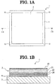
- An optical wavelength conversion device 1 shown in FIGS. 1A and 1B includes an optical wavelength conversion member 2, a heat dissipation member 3, and a joint portion 4.
- the optical wavelength conversion member 2 is a member which converts the wavelength of incident light.
- the optical wavelength conversion member 2 includes a plate-shaped ceramic fluorescent body 21, a reflecting film 22, an antireflection film 23, and an intermediate film 24.
- the ceramic fluorescent body 21 is a ceramic sintered body including a fluorescent phase containing fluorescent crystalline particles as a main component and a light-transmitting phase containing light-transmitting crystalline particles as a main component.
- the "fluorescent phase” is a phase containing fluorescent crystalline particles as a main component
- the "light-transmitting phase” is a phase containing, as a main component, light-transmitting crystalline particles, specifically, crystalline particles having a composition different from that of the crystalline particles in the fluorescent phase.
- the term "main component" means the highest content component of a phase.
- the fluorescent phase contains the fluorescent crystalline particles in an amount of 50% by volume or more and preferably 90% by volume or more.
- the light-transmitting phase contains the light-transmitting crystalline particles in an amount of 50% by volume or more and preferably 90% by volume or more.
- the light-transmitting phase used may be, for example, alumina or glass.
- the light-transmitting phase may be a single crystal.
- the crystalline particles in the ceramic sintered body forming the ceramic fluorescent body 21 and their grain boundaries may contain the light-transmitting phase and unavoidable impurities other than the light-transmitting phase.
- the crystalline particles in the light-transmitting phase may have a composition represented by chemical formula (1) Al 2 O 3
- the crystalline particles in the fluorescent phase may have a composition represented by chemical formula (2) A 3 B 5 O 12 :Ce (i.e., the garnet structure).
- a 3 B 5 O 12 :Ce means a solid solution in which Ce is dissolved in A 3 B 5 O 12 and part of the element A is replaced with Ce.
- the solute Ce imparts fluorescence to the crystalline particles in the fluorescent phase.
- the element A in chemical formula (1) and the element B in chemical formula (2) are each at least one element selected from the following groups of elements.
- the above ceramic sintered body is used as the ceramic fluorescent body 21
- light scattering occurs at the interface between the fluorescent phase and the light-transmitting phase, so that the angular dependence of the color of light can be reduced. This can improve color uniformity.
- the ceramic sintered body is excellent in thermal conductivity, so that heat generated by irradiation with laser light is easily dissipated to the heat dissipation member 3. Therefore, the fluorescent performance can be maintained even in a high laser power range.
- the ceramic fluorescent body 21 is a single component body, no light scattering occurs. In this case, the angular dependence of the color of light is large, and unevenness in the color of the light may occur.
- a resin is used for the fluorescent body, its thermal conductivity is low, so that heat dissipation is insufficient. In this case, temperature quenching may occur.
- the average thickness (i.e., the average distance from the upper surface to the lower surface) of the ceramic fluorescent body 21 is preferably from 100 ⁇ m to 500 ⁇ m inclusive.
- the reflecting film 22 is disposed on the lower surface of the ceramic fluorescent body 21 (i.e., its surface on the heat dissipation member 3 side).
- the reflecting film 22 reflects light generated inside the ceramic fluorescent body 21, so that the light is efficiently emitted to the outside of the optical wavelength conversion member 2.
- the light emission intensity of the optical wavelength conversion member 2 is thereby increased.
- Examples of the material used for the reflecting film 22 include, in addition to metals such as metallic aluminum and silver, niobium oxide, titanium oxide, lanthanum oxide, tantalum oxide, yttrium oxide, gadolinium oxide, tungsten oxide, hafnium oxide, aluminum oxide, and silicon nitride.
- metals such as metallic aluminum and silver, niobium oxide, titanium oxide, lanthanum oxide, tantalum oxide, yttrium oxide, gadolinium oxide, tungsten oxide, hafnium oxide, aluminum oxide, and silicon nitride.
- the average thickness of the reflecting film 22 is from 0.1 ⁇ m to 2 ⁇ m inclusive.
- the reflecting film 22 may have a single-layer structure or a multilayer structure.
- the antireflection film 23 is disposed on the upper surface of the ceramic fluorescent body 21 (i.e., its surface opposite to the heat dissipation member 3).
- the antireflection film 23 is an anti-reflection coating (AR coating) which prevents light reflection from the ceramic fluorescent body 21.
- the antireflection film 23 allows the ceramic fluorescent body 21 to absorb light efficiently. Moreover, light generated inside the ceramic fluorescent body 21 can be efficiently extracted to the outside. As a result, the light emission intensity of the optical wavelength conversion member 2 is increased.
- Examples of the material used for the antireflection film 23 include niobium oxide, titanium oxide, tantalum oxide, aluminum oxide, zirconium oxide, silicon oxide, aluminum nitride, silicon nitride, and magnesium fluoride.
- the average thickness of the antireflection film 23 is from 0.01 ⁇ m to 1 ⁇ m inclusive.
- the antireflection film 23 may have a single-layer structure or a multilayer structure.
- the intermediate film 24 is disposed on the lower surface of the reflecting film 22 (i.e., its surface opposite to the ceramic fluorescent body 21).
- the intermediate film 24 is disposed between the reflecting film 22 and the joint portion 4 described later. Specifically, the joint portion 4 is joined to the intermediate film 24 of the optical wavelength conversion member 2. The intermediate film 24 improves the bonding between the joint portion 4 and the optical wavelength conversion member 2.
- the intermediate film 24 includes a metal film and an oxide film.
- the material used for the metal film may be gold, silver, nickel, etc.
- the material used for the oxide film may be aluminum oxide, titanium oxide, etc.
- the intermediate film 24 includes a nickel film serving as the metal film and an aluminum oxide film serving as the oxide film.
- the average thickness of the intermediate film 24 is from 0.01 ⁇ m to 1 ⁇ m inclusive.
- At least one corner portion 12 of the optical wavelength conversion member 2 as viewed in its thickness direction is rounded. This reduces stress generated due to the difference in thermal expansion between the optical wavelength conversion member 2 and the heat dissipation member 3 when they are joined together. The joint strength is thereby improved, and heat dissipation is improved.
- stress generated in the optical wavelength conversion member 2 during irradiation with laser light tends to be uniform in plane directions. Therefore, forces acting on the upper and lower surfaces of the optical wavelength conversion member 2 can be reduced, so that breakage such as delamination of the optical wavelength conversion member 2 during operation can be prevented.
- the heat dissipation member 3 is more excellent in heat dissipation than the optical wavelength conversion member 2.
- the heat dissipation member 3 is attached to the optical wavelength conversion member 2 through the joint portion 4.
- the heat dissipation member 3 facilitates dissipation of the heat generated in the ceramic fluorescent body 21 due to irradiation with laser light. As a result, the fluorescent performance of the ceramic fluorescent body 21 in a high power range is maintained.
- the material used for the heat dissipation member 3 may be copper, aluminum, aluminum nitride, etc. Of these, copper is preferred.
- the heat dissipation member 3 may have a main body made of a metal and an oxide film formed on the surface of the main body. The oxide film improves the joint strength with the joint portion 4.
- the heat dissipation member 3 is formed into, for example, a plate shape.
- the heat dissipation member 3 may have a plate-shaped portion and at least one heat radiation fin protruding from the plate-shaped portion.
- the average thickness of the plate-shaped portion of the heat dissipation member 3 is preferably from 0.1 mm to 5 mm inclusive.
- FSW friction stir welding
- the joint portion 4 joins the optical wavelength conversion member 2 and the heat dissipation member 3 together.
- the joint portion 4 is disposed between the lower surface of the intermediate film 24 of the optical wavelength conversion member 2 and the upper surface of the heat dissipation member 3 (i.e., its surface on the optical wavelength conversion member 2 side) and joins these two surfaces together.
- the melting point of the joint portion 4 is 240°C or higher. If the melting point of the joint portion 4 is lower than 240°C, the joint portion 4 melts due to heat from the optical wavelength conversion member 2 when the laser is in a high power range, and a defect such as delamination or breakage thereby occurs.
- the melting point of the joint portion 4 is preferably 300°C or higher, more preferably 500°C or higher, and still more preferably 800°C or higher.
- the thermal conductivity of the joint portion 4 is 120 W/mK or higher.
- a thermal conductivity of the joint portion 4 of less than 120 W/mK may be insufficient to dissipate heat from the optical wavelength conversion member 2 more effectively, and the fluorescent performance in a high laser power range may decrease.
- the thermal conductivity of the joint portion 4 is preferably 150 W/mK or higher.
- the thermal conductivity of the joint portion 4 can be measured by, for example, a light pulse thermoreflectance method. Specifically, the optical wavelength conversion device 1 is cut obliquely with respect to its incident surface to expose the joint portion 4. The exposed portion is irradiated with pulsed light and laser light, and the reflected laser light is measured to obtain the thermal resistance of the joint portion 4. The thermal conductivity is computed from the obtained thermal resistance and the area and thickness of the joint portion 4.
- the material of the joint portion 4 is not limited to the material of the joint portion 4, so long as at least the melting point of the joint portion 4 satisfies the above condition. However, it is more preferable that the melting point and thermal conductivity of the joint portion 4 satisfy the above conditions. Moreover, to satisfy the above conditions, the joint portion 4 may be formed only of gold, silver, copper, or a combination thereof.
- the joint portion 4 may have pores. When the joint portion 4 has pores, the difference in thermal expansion between the heat dissipation member 3 and the optical wavelength conversion member 2 is reduced, so that breakage of the joint portion 4 due to thermal shock can be prevented.
- the joint portion 4 having pores can be obtained, for example, by sintering nanoparticles of any of the above metals.
- the nanoparticles are a group of particles having an average diameter of several nanometers to several micrometers and including particles whose sizes are on the order of nanometer.
- the joint portion 4 is preferably a sintered body of metal nanoparticles. In this sintered body, spaces between the nanoparticles bonded together by sintering serve as pores.
- the maximum width of the pores i.e., the maximum pore diameter
- the porosity of the joint portion 4 is preferably from 1% to 40% inclusive. If the porosity is less than 1%, the effect of reducing the difference in thermal expansion between the heat dissipation member 3 and the optical wavelength conversion member 2 may not be obtained. If the porosity exceeds 40%, the heat transferability of the joint portion 4 may decrease, and this may cause a reduction in the heat dissipation efficiency of the optical wavelength conversion member 2.
- the “porosity” is determined, for example, as the ratio of the area of the pores in an observation cross section obtained by observing a cross section of the joint portion 4 under a scanning electron microscope (SEM) (i.e., the ratio of the total area of the pores to the total area of the pores and a material layer).
- SEM scanning electron microscope
- the upper surface of the joint portion 4 (i.e., its surface on the optical wavelength conversion member 2 side) is joined to the entire lower surface of the optical wavelength conversion member 2.
- the joint portion 4 is disposed in the form of a layer only in a region sandwiched between the optical wavelength conversion member 2 and the heat dissipation member 3 (i.e., in part of the upper surface of the heat dissipation member 3) .
- the joint portion 4 may be disposed in a region larger than the lower surface of the optical wavelength conversion member 2 and may be disposed so as to cover the entire upper surface of the heat dissipation member 3. As shown in FIG. 2 , the joint portion 4 may be disposed so as to cover the side surfaces of the optical wavelength conversion member 2 (i.e., its surfaces parallel to the thickness direction). When the joint portion 4 covers the side surfaces of the optical wavelength conversion member 2, the joint portion 4 may also cover part of the upper surface of the optical wavelength conversion member 2 (i.e., the upper surface of the antireflection film 23).
- the average thickness of a joint region disposed between the optical wavelength conversion member 2 and the heat dissipation member 3 is preferably 1 ⁇ m or more. If the average thickness of the joint region is less than 1 ⁇ m, the joint strength of the joint portion 4 may be insufficient. Moreover, a sufficient heat dissipation path may not be provided between the optical wavelength conversion member 2 and the heat dissipation member 3.
- the average thickness of the joint region is preferably equal to or less than 50% of the sum of the average thickness of the ceramic fluorescent body 21 and the average thickness of the joint region (the sum will be referred to as the total thickness). If the average thickness of the joint region exceeds 50% of the total thickness, the distance from the ceramic fluorescent body 21 to the heat dissipation member 3 is larger than the thickness of the ceramic fluorescent body 21. In this case, it is difficult to transfer the heat generated in the optical wavelength conversion member 2 rapidly to the heat dissipation member 3, and therefore the heat dissipation efficiency may deteriorate.
- An optical composite device 10 shown in FIG. 3 includes the optical wavelength conversion device 1 and a package 5 which houses the optical wavelength conversion device 1.
- the package 5 is a box-shaped container or a plate-shaped substrate.
- the package 5 contains, as a main component, a ceramic such as alumina.
- the "main component” means a component contained in an amount of, for example, 80% by mass or more.
- the package 5 may have a light emitting element-mounting region for mounting a light emitting element such as an LED or an LD.
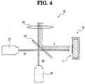
- the optical composite device 10 is used for a light source unit 20 shown in FIG. 4 .
- the light source unit 20 includes the optical composite device 10, a plurality of well-known blue laser oscillators (i.e., a first blue laser oscillator 27 and a second blue laser oscillator 29) each including a light-emitting element etc., a dichroic mirror 25, and a lens 26.
- first blue light B1 is emitted in the right direction in FIG. 4 from the first blue laser oscillator 27 toward the optical wavelength conversion device 1.
- the first blue light B1 is wavelength-converted and reflected by the optical wavelength conversion device 1 and is outputted as yellow light Y in the left direction in FIG. 4 .
- the yellow light Y is reflected by the dichroic mirror 25 inclined 45° with respect to the left-right direction in FIG. 4 and is outputted toward the lens 26.
- Second blue light B2 emitted in the upward direction in FIG. 4 from the second blue laser oscillator 29 toward the lens 26 passes through the dichroic mirror 25 and is outputted toward the lens 26 without any conversion.
- the first blue light B1 and the yellow light Y are thereby mixed in the lens 26, and white light is generated. Therefore, in the light source unit 20, the white light is outputted upward in FIG. 4 from the lens 26.
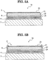
- Optical wavelength conversion devices 1A shown in FIGS. 5A and 5B each include the optical wavelength conversion member 2, the heat dissipation member 3, the joint portion 4, and a resin layer 6.
- optical wavelength conversion member 2 Since the optical wavelength conversion member 2, the heat dissipation member 3, and the joint portion 4 are the same as those of the optical wavelength conversion device 1 in FIGS. 1A and 1B , they are denoted by the same reference numerals, and their description will be omitted.
- the resin layer 6 at least partially covers (i.e., coats) a surface of the joint portion 4 which is not joined to the optical wavelength conversion member 2 and to the heat dissipation member 3.
- the resin layer 6 covers the entire side surfaces of the joint portion 4 and part of the side surfaces of the optical wavelength conversion member 2.
- the resin layer 6 also covers part of the upper surface of the heat dissipation member 3.
- the resin layer 6 in FIG. 5A extends from the upper surface of the heat dissipation member 3 to the side surfaces of the ceramic fluorescent body 21.
- the resin layer 6 may cover the entire side surfaces of the optical wavelength conversion member 2. As shown in FIG. 5B , the resin layer 6 may cover part of the upper surface of the optical wavelength conversion member 2 (i.e., the upper surface of the antireflection film 23) in addition to the entire side surfaces of the optical wavelength conversion member 2.
- the main component of the resin layer 6 is preferably a fluoride-based resin.
- the use of the fluoride-based resin allows the resin layer 6 to have reduced permeability to water and gases such as O 2 , H 2 S, and SO 2 , and oxidation (particularly in the case where copper is used for the joint portion 4), sulfurization (particularly in the case where silver is used for the joint portion 4), etc. at the interfaces of the joint portion 4 can be effectively prevented.
- An optical wavelength conversion device 1B shown in FIGS. 6A and 6B includes the optical wavelength conversion member 2, a heat dissipation member 3B, and the joint portion 4.
- optical wavelength conversion member 2 and the joint portion 4 are the same as those of the optical wavelength conversion device 1 in FIGS. 1A and 1B , they are denoted by the same reference numerals, and their description will be omitted.
- the heat dissipation member 3B of the present embodiment has a notch 13 disposed on its surface joined to the joint portion 4 (i.e., on the upper surface).
- the notch 13 is an annular groove disposed around the optical wavelength conversion member 2 and recessed toward the side opposite to the joint portion 4.
- the notch 13 is formed such that its inner edge is flush with the side surfaces of the optical wavelength conversion member 2 and the side surfaces of the joint portion 4.
- the notch 13 is disposed at a position which does not overlap the optical wavelength conversion member 2 and the joint portion 4 in the thickness direction. Specifically, the notch 13 is not joined to the joint portion 4 and is exposed at the upper surface of the heat dissipation member 3B.
- the notch 13 may be disposed at a position overlapping the optical wavelength conversion member 2 and the joint portion 4.
- the notch 13 is not limited to the annular notch.
- the heat dissipation member 3B may have a plurality of notches 13.
- the notch 13 of the heat dissipation member 3B can reduce stress generated due to the difference in thermal expansion between the optical wavelength conversion member 2 and the heat dissipation member 3 when they are joined together. Therefore, the joint strength is improved, and the heat dissipation is improved. Moreover, since thermal stress generated in the heat dissipation member 3B in a high temperature environment is reduced, breakage such as delamination of the optical wavelength conversion member 2 during operation can be prevented.
- Particles of Al 2 O 3 (average particle diameter: 0.2 ⁇ m), particles of Y 2 O 3 (average particle diameter: 1.2 ⁇ m), particles of Gd 2 O 3 (average particle diameter: 1.1 ⁇ m), and particles of CeO 2 (average particle diameter: 1.5 ⁇ m) were weighed such that the amount of A 3 B 5 O 12 :Ce was 30% by volume with respect to the total volume of a sintered body.
- the ceramic fluorescent body obtained was shaped into a 16 mm by 16 mm square plate with an average thickness of 200 ⁇ m.
- An antireflection film was formed on the upper surface of the ceramic fluorescent body, and a reflecting film and an intermediate film were formed on the lower surface to thereby obtain an optical wavelength conversion member.
- the antireflection film formed was a multilayer coating including an SiO 2 layer and a Ta 2 O 5 layer
- the reflecting film formed was a multilayer coating including a TiO 2 layer and an Ag layer
- the intermediate film formed was a multilayer coating including a Ni layer and an Al 2 O 3 layer.
- the optical wavelength conversion member obtained through the above steps was cut into a 3.5 mm by 3.5 mm square piece.
- a copper-made heat dissipation member was cut into a 12 mm by 12 mm square plate with an average thickness of 2 mm.
- Silver nanoparticles, copper nanoparticles, or a particle mixture of the silver nanoparticles and the copper nanoparticles disposed between the cut optical wavelength conversion member and the cut heat dissipation member was sintered to form a joint portion.
- optical wavelength conversion device samples 1 to 3 were obtained. The melting point and thermal conductivity of the joint portion in each sample are shown in Tale 1.
- Each sample was irradiated with laser light having a wavelength of 465 nm (i.e., blue LD light) and focused through a lens to a width of 1 mm.
- the X chromaticity value of the light reflected from each sample was measured using a spectroradiometer ("CL-500A" manufactured by KONICA MINOLTA, INC.). In this measurement, the power density of the blue LD light used for irradiation was gradually increased from 0 W/mm 2 to 200 W/mm 2 .
- the power density when the chromaticity value was reduced to 60% or less of the chromaticity value at a power density of 5 W/mm 2 was determined as a power density at which temperature quenching had occurred and used as the laser power resistance performance of the sample.
- the results are shown in Table 1. When the laser power resistance performance is 90 W/mm 2 or more, the laser power resistance performance is judged as good.
- Each sample was subjected to thermal cycles in which the temperature of the atmosphere was repeatedly changed from -50°C to 150°C. After 1000 cycles, the laser power resistance performance was evaluated, and the ratio of the laser power resistance performance after the thermal cycles to the laser power resistance performance before the thermal cycles was determined. This ratio is preferably 80% or more.
- An optical wavelength conversion member and a heat dissipation member identical to those in Example 1 were prepared, and a silicone paste (thermal conductivity: 0.9 W/mK), a conductive paste containing silver (thermal conductivity: 14 W/mK), and solder (thermal conductivity: 60 W/mK) were used to form respective joint portions to thereby obtain optical wavelength conversion device samples 4 to 6.
- a silicone paste thermal conductivity: 0.9 W/mK
- a conductive paste containing silver thermal conductivity: 14 W/mK
- solder thermo conductivity: 60 W/mK
- optical wavelength conversion member and a heat dissipation member identical to those in Example 1 were prepared, and silver nanoparticles were used to form a joint portion having a porosity different from that in Example 1.
- optical wavelength conversion device samples 7 to 12 were obtained.
- the results of measurement of the laser power resistance performance and porosity of each sample are shown in Table 1.
- Optical wavelength conversion device samples 13 to 24 were obtained by the same procedure as in Example 1 except that Al 2 O 3 particles (average particle diameter: 0.2 ⁇ m), Y 2 O 3 particles (average particle diameter: 1.2 ⁇ m), Gd 2 O 3 particles (average particle diameter: 1.1 ⁇ m), CeO 2 particles (average particle diameter: 1.5 ⁇ m), Lu 2 O 3 particles (average particle diameter: 1.1 ⁇ m), Sc 2 O 3 particles (average particle diameter: 1.2 ⁇ m), and Ga 2 O 3 particles (average particle diameter: 1.1 ⁇ m) were weighed such that the amount of A 3 B 5 O 12 :Ce was 30% by volume with respect to the total volume of a sintered body and that a composition shown in Table 1 was obtained. The results of measurement of the laser power resistance performance and porosity of each sample are shown in Table 1.
- Optical wavelength conversion device samples 25 to 30 were obtained by the same procedure as in Example 1 except that the average thickness of the ceramic fluorescent body and the average thickness of the joint region in the joint portion were changed as shown in Table 1. The results of measurement of the laser power resistance performance and porosity of each sample are shown in Table 1. In sample 30, the laser power resistance performance could not be measured because of insufficient strength of the joint portion.
- An optical wavelength conversion device sample 31 was obtained by the same procedure as in Example 1 except that the side surfaces of the joint portion were covered with a fluorine-based resin layer.
- An optical wavelength conversion device sample 32 was obtained by the same procedure as in Example 1 except that a notch was formed on the upper surface of the heat dissipation member.
- An optical wavelength conversion device sample 33 was obtained by the same procedure as in Example 1 except that corner portions of the optical wavelength conversion member when it was viewed in its thickness direction were rounded so as to have a radius of 5 mm.
- optical wavelength conversion devices in which the porosity of the joint portion is 40% or less can be used in a higher power range.
- optical wavelength conversion devices whose ceramic fluorescent bodies have different compositions can be used in a high power range.
- optical wavelength conversion devices in which the ratio of the average thickness of the joint region in the joint portion to the total thickness of the ceramic fluorescent body and the joint region ("average thickness ratio of joint portion" in Table 1) is 50% or less can be used in a higher power range.
- Example 5 when the joint portion is covered with the resin layer, a decrease in laser power resistance performance after heating at high temperature for a long time can be suppressed. As can be seen, the notch and the rounded corner portions improve the joint strength of each optical wavelength conversion device, and the laser power resistance performance is improved.
Landscapes
- Physics & Mathematics (AREA)
- Engineering & Computer Science (AREA)
- General Engineering & Computer Science (AREA)
- General Physics & Mathematics (AREA)
- Optics & Photonics (AREA)
- Spectroscopy & Molecular Physics (AREA)
- Semiconductor Lasers (AREA)
- Optical Filters (AREA)
Abstract

Description
- This international patent application claims priority from Japanese Patent Application No.
2018-24282 2018-24282 - The present disclosure relates to an optical wavelength conversion device.
- In headlamps, various lighting fixtures, laser projectors, etc., white light is obtained by converting the wavelength of blue light from a light emitting diode (LED) or a semiconductor laser diode (LD) using a fluorescent body serving as an optical wavelength conversion member.
- Known examples of the fluorescent body include resin-based and glass-based fluorescent bodies. To cope with increasing output power of light sources using lasers, ceramic fluorescent bodies excellent in durability are increasingly used for optical wavelength conversion devices.
- The fluorescent body generates heat when irradiated with light. When the fluorescent body generates heat and its temperature increases, temperature quenching occurs, in which the fluorescent performance of the fluorescent body such as the intensity of light emitted therefrom (i.e., light emission intensity: fluorescence intensity) decreases. Therefore, to allow the fluorescent body to emit light efficiently, it is necessary to dissipate the heat from the fluorescent body to the outside.
- In one known optical wavelength conversion device, a heat dissipation member is soldered to an optical wavelength conversion member (see Patent Document 1). However, the melting point of the solder is 200°C or lower. Therefore, in the above optical wavelength conversion device, heat generated from the fluorescent body irradiated with laser light may re-melt the solder, causing a reduction in the joint strength between the heat dissipation member and the optical wavelength conversion member. This causes a defect such as breakage or detachment of the optical wavelength conversion member from the heat dissipation member.
- Moreover, the defect results in insufficient heat transfer from the optical wavelength conversion member to the heat dissipation member, so that heat dissipation efficiency lowers. This problem also occurs even when a resin-based adhesive is used instead of the solder for joining.
- In an optical wavelength conversion device devised in view of the above, silver nanoparticles are used to join the optical wavelength conversion member to the heat dissipation member (see Patent Document 2).
-
- Patent Document 1: International Publication No.
WO2014/065051 - Patent Document 2: International Publication No.
WO2017/110031 - In the optical wavelength conversion device using the silver nanoparticles, the occurrence of a defect due to re-melting of solder can be prevented. However, in this optical wavelength conversion device, there is a room for improvement in heat transferability from the optical wavelength conversion member to the heat dissipation member.
- One aspect of the present disclosure preferably provides an optical wavelength conversion device in which heat can be efficiently dissipated from the optical wavelength conversion member while the joint strength between the optical wavelength conversion member and the heat dissipation member is maintained.
- One mode of the present disclosure is an optical wavelength conversion device comprising an optical wavelength conversion member configured to convert the wavelength of incident light; a heat dissipation member which is more excellent in heat dissipation than the optical wavelength conversion member; and a joint portion which joins the optical wavelength conversion member and the heat dissipation member together. The optical wavelength conversion member includes a plate-shaped ceramic fluorescent body, and a reflecting film disposed on a heat dissipation member-side surface of the ceramic fluorescent body. The joint portion has a thermal conductivity of 120 W/mK or more. The joint portion has a melting point of 240°C or higher.
- In the above structure, the heat dissipation performance of the joint portion serving as a heat dissipation path between the optical wavelength conversion member and the heat dissipation member can be increased, so that heat can be more efficiently dissipated from the optical wavelength conversion member.
- Moreover, even when the temperature of the ceramic fluorescent body increases due to laser irradiation, the joint portion joining the optical wavelength conversion member and the heat dissipation member together is unlikely to melt. Therefore, high heat resistance and high joint strength can be maintained even in a high laser power range. Thus, the heat dissipation path between the optical wavelength conversion member and the heat dissipation member can be maintained even in the high power range, and heat can be dissipated from the optical wavelength conversion member efficiently.
- In the one mode of the present disclosure, the joint portion may be formed only of gold, silver, copper, or a combination thereof. In this structure, the joint portion which allows the heat to be dissipated from the optical wavelength conversion member efficiently can be formed easily and reliably.
- In the one mode of the present disclosure, the joint portion may have pores. The joint portion may have a porosity of 40% or less. In this structure, while the heat dissipation performance of the joint portion is maintained, the difference in thermal expansion between the heat dissipation member and the optical wavelength conversion member is reduced, so that breakage of the joint portion due to thermal shock can be prevented.
- In the one mode of the present disclosure, the joint portion may have a joint region located between the optical wavelength conversion member and the heat dissipation member and having an average thickness of 1 µm or more. In this structure, the joint strength between the optical wavelength conversion member and the heat dissipation member can be increased further.
- In the one mode of the present disclosure, the joint portion may have a joint region located between the optical wavelength conversion member and the heat dissipation member and having an average thickness equal to or less than 50% of the sum of the average thickness of the ceramic fluorescent body and the average thickness of the joint region. In this structure, an excessive increase in the thickness of the joint region is prevented, and the heat generated in the optical wavelength conversion member can be more rapidly transferred to the heat dissipation member. Therefore, the heat can be more efficiently dissipated from the optical wavelength conversion member.
- The one mode of the present disclosure may further comprise a resin layer which at least partially covers a surface of the joint portion which is not joined to the optical wavelength conversion member and to the heat dissipation member. In this structure, oxidation, sulfurization, etc. at the joint interfaces of the joint portion can be prevented. Therefore, the durability of the optical wavelength conversion device can be improved.
- In the one mode of the present disclosure, the resin layer may contain a fluorine-based resin as a main component. In this structure, the resin layer can have reduced permeability to water and gases such as O2, H2S, and SO2, so that the durability of the optical wavelength conversion device can be improved more reliably.
- In the one mode of the present disclosure, the heat dissipation member may have at least one notch on its surface joined to the joint portion. In this structure, stress generated due to the difference in thermal expansion between the optical wavelength conversion member and the heat dissipation member when they are joined together can be reduced. Therefore, the joint strength is improved, and the heat dissipation is improved. Moreover, since thermal stress generated in the heat dissipation member in a high temperature environment is reduced, breakage such as delamination of the optical wavelength conversion member during operation can be prevented.
- In the one mode of the present disclosure, at least one corner portion of the optical wavelength conversion member as viewed in a thickness direction thereof may be rounded. In this structure, stress generated due to the difference in thermal expansion between the optical wavelength conversion member and the heat dissipation member when they are joined together can be reduced. Therefore, the joint strength is improved, and the heat dissipation is improved. Moreover, stress generated in the optical wavelength conversion member during irradiation with laser light tends to be uniform in plane directions. Therefore, forces acting on the upper and lower surfaces of the optical wavelength conversion member can be reduced, so that breakage such as delamination of the optical wavelength conversion member during operation can be prevented.
-
- [
FIG. 1] FIG. 1A is a schematic plan view of an optical wavelength conversion device of an embodiment, andFIG. 1B is a schematic cross-sectional view taken along line IB-IB inFIG. 1A . - [
FIG. 2] FIG. 2 is a schematic cross-sectional view of an optical wavelength conversion device of an embodiment different from that shown inFIG. 1B . - [
FIG. 3] FIG. 3 is a schematic cross-sectional view of an optical composite device provided with the optical wavelength conversion device of one of the embodiments. - [
FIG. 4] FIG. 4 is an illustration of a light source unit. - [
FIG. 5] FIG. 5A is a schematic cross-sectional view of an optical wavelength conversion device of an embodiment different from those shown inFIGS. 1B and2 , andFIG. 5B is a schematic cross-sectional view of an optical wavelength conversion device of an embodiment different from those shown inFIGS. 1A, 1B ,2 , and5A . - [
FIG. 6 ]FIG. 6A is a schematic plan view of an optical wavelength conversion device of an embodiment different from those inFIGS. 1A, 1B ,2 ,5A, and 5B , andFIG. 6B is a schematic cross-sectional view taken along line VIB-VIB inFIG. 6A . - 1, 1A, 1B ··· optical wavelength conversion device, 2 ··· optical wavelength conversion member, 3, 3B ··· heat dissipation member, 4 ··· joint portion, 5 ··· package, 6 ··· resin layer, 10 ··· optical composite device, 12 ··· corner portion, 13 ··· notch, 20 ··· light source unit, 21 ... ceramic fluorescent body, 22 ··· reflecting film, 23 ... antireflection film, 24 ··· intermediate film, 25 ··· dichroic mirror, 26 ··· lens, 27 ··· first blue laser oscillator , 29 ··· second blue laser oscillator
- Embodiments to which the present disclosure is applied will be described with reference to the drawings.
- An optical
wavelength conversion device 1 shown inFIGS. 1A and 1B includes an opticalwavelength conversion member 2, aheat dissipation member 3, and ajoint portion 4. - The optical
wavelength conversion member 2 is a member which converts the wavelength of incident light. The opticalwavelength conversion member 2 includes a plate-shaped ceramicfluorescent body 21, a reflectingfilm 22, anantireflection film 23, and anintermediate film 24. - The ceramic
fluorescent body 21 is a ceramic sintered body including a fluorescent phase containing fluorescent crystalline particles as a main component and a light-transmitting phase containing light-transmitting crystalline particles as a main component. - The "fluorescent phase" is a phase containing fluorescent crystalline particles as a main component, and the "light-transmitting phase" is a phase containing, as a main component, light-transmitting crystalline particles, specifically, crystalline particles having a composition different from that of the crystalline particles in the fluorescent phase.
- The term "main component" means the highest content component of a phase. For example, the fluorescent phase contains the fluorescent crystalline particles in an amount of 50% by volume or more and preferably 90% by volume or more. For example, the light-transmitting phase contains the light-transmitting crystalline particles in an amount of 50% by volume or more and preferably 90% by volume or more. The light-transmitting phase used may be, for example, alumina or glass. The light-transmitting phase may be a single crystal.
- The crystalline particles in the ceramic sintered body forming the ceramic
fluorescent body 21 and their grain boundaries may contain the light-transmitting phase and unavoidable impurities other than the light-transmitting phase. - No particular limitation is imposed on the materials of the ceramic
fluorescent body 21. For example, the crystalline particles in the light-transmitting phase may have a composition represented by chemical formula (1) Al2O3, and the crystalline particles in the fluorescent phase may have a composition represented by chemical formula (2) A3B5O12:Ce (i.e., the garnet structure). - Notably, "A3B5O12:Ce" means a solid solution in which Ce is dissolved in A3B5O12 and part of the element A is replaced with Ce. The solute Ce imparts fluorescence to the crystalline particles in the fluorescent phase.
- The element A in chemical formula (1) and the element B in chemical formula (2) are each at least one element selected from the following groups of elements.
- A: Sc, Y, and lanthanoids (except for Ce)
(Gd may be further contained as A) - B: Al (Ga may be further contained as B)
- When the above ceramic sintered body is used as the ceramic
fluorescent body 21, light scattering occurs at the interface between the fluorescent phase and the light-transmitting phase, so that the angular dependence of the color of light can be reduced. This can improve color uniformity. - The ceramic sintered body is excellent in thermal conductivity, so that heat generated by irradiation with laser light is easily dissipated to the
heat dissipation member 3. Therefore, the fluorescent performance can be maintained even in a high laser power range. - When the ceramic
fluorescent body 21 is a single component body, no light scattering occurs. In this case, the angular dependence of the color of light is large, and unevenness in the color of the light may occur. When a resin is used for the fluorescent body, its thermal conductivity is low, so that heat dissipation is insufficient. In this case, temperature quenching may occur. - The average thickness (i.e., the average distance from the upper surface to the lower surface) of the ceramic
fluorescent body 21 is preferably from 100 µm to 500 µm inclusive. - The reflecting
film 22 is disposed on the lower surface of the ceramic fluorescent body 21 (i.e., its surface on theheat dissipation member 3 side). - The reflecting
film 22 reflects light generated inside the ceramicfluorescent body 21, so that the light is efficiently emitted to the outside of the opticalwavelength conversion member 2. The light emission intensity of the opticalwavelength conversion member 2 is thereby increased. - Examples of the material used for the reflecting
film 22 include, in addition to metals such as metallic aluminum and silver, niobium oxide, titanium oxide, lanthanum oxide, tantalum oxide, yttrium oxide, gadolinium oxide, tungsten oxide, hafnium oxide, aluminum oxide, and silicon nitride. - Preferably, the average thickness of the reflecting
film 22 is from 0.1 µm to 2 µm inclusive. - The reflecting
film 22 may have a single-layer structure or a multilayer structure. - The
antireflection film 23 is disposed on the upper surface of the ceramic fluorescent body 21 (i.e., its surface opposite to the heat dissipation member 3). - The
antireflection film 23 is an anti-reflection coating (AR coating) which prevents light reflection from the ceramicfluorescent body 21. Theantireflection film 23 allows the ceramicfluorescent body 21 to absorb light efficiently. Moreover, light generated inside the ceramicfluorescent body 21 can be efficiently extracted to the outside. As a result, the light emission intensity of the opticalwavelength conversion member 2 is increased. - Examples of the material used for the
antireflection film 23 include niobium oxide, titanium oxide, tantalum oxide, aluminum oxide, zirconium oxide, silicon oxide, aluminum nitride, silicon nitride, and magnesium fluoride. - Preferably, the average thickness of the
antireflection film 23 is from 0.01 µm to 1 µm inclusive. - The
antireflection film 23 may have a single-layer structure or a multilayer structure. - The
intermediate film 24 is disposed on the lower surface of the reflecting film 22 (i.e., its surface opposite to the ceramic fluorescent body 21). - The
intermediate film 24 is disposed between the reflectingfilm 22 and thejoint portion 4 described later. Specifically, thejoint portion 4 is joined to theintermediate film 24 of the opticalwavelength conversion member 2. Theintermediate film 24 improves the bonding between thejoint portion 4 and the opticalwavelength conversion member 2. - The
intermediate film 24 includes a metal film and an oxide film. - The material used for the metal film may be gold, silver, nickel, etc. The material used for the oxide film may be aluminum oxide, titanium oxide, etc.
- Preferably, the
intermediate film 24 includes a nickel film serving as the metal film and an aluminum oxide film serving as the oxide film. - Preferably, the average thickness of the
intermediate film 24 is from 0.01 µm to 1 µm inclusive. - As shown in
FIG. 1A , at least onecorner portion 12 of the opticalwavelength conversion member 2 as viewed in its thickness direction is rounded. This reduces stress generated due to the difference in thermal expansion between the opticalwavelength conversion member 2 and theheat dissipation member 3 when they are joined together. The joint strength is thereby improved, and heat dissipation is improved. - Moreover, stress generated in the optical
wavelength conversion member 2 during irradiation with laser light tends to be uniform in plane directions. Therefore, forces acting on the upper and lower surfaces of the opticalwavelength conversion member 2 can be reduced, so that breakage such as delamination of the opticalwavelength conversion member 2 during operation can be prevented. - The
heat dissipation member 3 is more excellent in heat dissipation than the opticalwavelength conversion member 2. Theheat dissipation member 3 is attached to the opticalwavelength conversion member 2 through thejoint portion 4. - The
heat dissipation member 3 facilitates dissipation of the heat generated in the ceramicfluorescent body 21 due to irradiation with laser light. As a result, the fluorescent performance of the ceramicfluorescent body 21 in a high power range is maintained. - The material used for the
heat dissipation member 3 may be copper, aluminum, aluminum nitride, etc. Of these, copper is preferred. Theheat dissipation member 3 may have a main body made of a metal and an oxide film formed on the surface of the main body. The oxide film improves the joint strength with thejoint portion 4. - The
heat dissipation member 3 is formed into, for example, a plate shape. Theheat dissipation member 3 may have a plate-shaped portion and at least one heat radiation fin protruding from the plate-shaped portion. The average thickness of the plate-shaped portion of theheat dissipation member 3 is preferably from 0.1 mm to 5 mm inclusive. - To join the heat radiation fin and the plate-shaped portion together, friction stir welding (FSW) may be used. The FSW is a joining method for integrating members to be joined, and an increase in thermal resistance at the joint interface can be suppressed. Therefore, a reduction in the heat dissipation effect can be suppressed.
- The
joint portion 4 joins the opticalwavelength conversion member 2 and theheat dissipation member 3 together. In the present embodiment, thejoint portion 4 is disposed between the lower surface of theintermediate film 24 of the opticalwavelength conversion member 2 and the upper surface of the heat dissipation member 3 (i.e., its surface on the opticalwavelength conversion member 2 side) and joins these two surfaces together. - The melting point of the
joint portion 4 is 240°C or higher. If the melting point of thejoint portion 4 is lower than 240°C, thejoint portion 4 melts due to heat from the opticalwavelength conversion member 2 when the laser is in a high power range, and a defect such as delamination or breakage thereby occurs. The melting point of thejoint portion 4 is preferably 300°C or higher, more preferably 500°C or higher, and still more preferably 800°C or higher. - The thermal conductivity of the
joint portion 4 is 120 W/mK or higher. A thermal conductivity of thejoint portion 4 of less than 120 W/mK may be insufficient to dissipate heat from the opticalwavelength conversion member 2 more effectively, and the fluorescent performance in a high laser power range may decrease. The thermal conductivity of thejoint portion 4 is preferably 150 W/mK or higher. - The thermal conductivity of the
joint portion 4 can be measured by, for example, a light pulse thermoreflectance method. Specifically, the opticalwavelength conversion device 1 is cut obliquely with respect to its incident surface to expose thejoint portion 4. The exposed portion is irradiated with pulsed light and laser light, and the reflected laser light is measured to obtain the thermal resistance of thejoint portion 4. The thermal conductivity is computed from the obtained thermal resistance and the area and thickness of thejoint portion 4. - No particular limitation is imposed on the material of the
joint portion 4, so long as at least the melting point of thejoint portion 4 satisfies the above condition. However, it is more preferable that the melting point and thermal conductivity of thejoint portion 4 satisfy the above conditions. Moreover, to satisfy the above conditions, thejoint portion 4 may be formed only of gold, silver, copper, or a combination thereof. - The
joint portion 4 may have pores. When thejoint portion 4 has pores, the difference in thermal expansion between theheat dissipation member 3 and the opticalwavelength conversion member 2 is reduced, so that breakage of thejoint portion 4 due to thermal shock can be prevented. - The
joint portion 4 having pores can be obtained, for example, by sintering nanoparticles of any of the above metals. The nanoparticles are a group of particles having an average diameter of several nanometers to several micrometers and including particles whose sizes are on the order of nanometer. Thejoint portion 4 is preferably a sintered body of metal nanoparticles. In this sintered body, spaces between the nanoparticles bonded together by sintering serve as pores. The maximum width of the pores (i.e., the maximum pore diameter) is preferably 5 µm or less. - The porosity of the
joint portion 4 is preferably from 1% to 40% inclusive. If the porosity is less than 1%, the effect of reducing the difference in thermal expansion between theheat dissipation member 3 and the opticalwavelength conversion member 2 may not be obtained. If the porosity exceeds 40%, the heat transferability of thejoint portion 4 may decrease, and this may cause a reduction in the heat dissipation efficiency of the opticalwavelength conversion member 2. - The "porosity" is determined, for example, as the ratio of the area of the pores in an observation cross section obtained by observing a cross section of the
joint portion 4 under a scanning electron microscope (SEM) (i.e., the ratio of the total area of the pores to the total area of the pores and a material layer). - The upper surface of the joint portion 4 (i.e., its surface on the optical
wavelength conversion member 2 side) is joined to the entire lower surface of the opticalwavelength conversion member 2. In the present embodiment, thejoint portion 4 is disposed in the form of a layer only in a region sandwiched between the opticalwavelength conversion member 2 and the heat dissipation member 3 (i.e., in part of the upper surface of the heat dissipation member 3) . - However, the
joint portion 4 may be disposed in a region larger than the lower surface of the opticalwavelength conversion member 2 and may be disposed so as to cover the entire upper surface of theheat dissipation member 3. As shown inFIG. 2 , thejoint portion 4 may be disposed so as to cover the side surfaces of the optical wavelength conversion member 2 (i.e., its surfaces parallel to the thickness direction). When thejoint portion 4 covers the side surfaces of the opticalwavelength conversion member 2, thejoint portion 4 may also cover part of the upper surface of the optical wavelength conversion member 2 (i.e., the upper surface of the antireflection film 23). - In the
joint portion 4, the average thickness of a joint region disposed between the opticalwavelength conversion member 2 and theheat dissipation member 3 is preferably 1 µm or more. If the average thickness of the joint region is less than 1 µm, the joint strength of thejoint portion 4 may be insufficient. Moreover, a sufficient heat dissipation path may not be provided between the opticalwavelength conversion member 2 and theheat dissipation member 3. - The average thickness of the joint region is preferably equal to or less than 50% of the sum of the average thickness of the ceramic
fluorescent body 21 and the average thickness of the joint region (the sum will be referred to as the total thickness). If the average thickness of the joint region exceeds 50% of the total thickness, the distance from the ceramicfluorescent body 21 to theheat dissipation member 3 is larger than the thickness of the ceramicfluorescent body 21. In this case, it is difficult to transfer the heat generated in the opticalwavelength conversion member 2 rapidly to theheat dissipation member 3, and therefore the heat dissipation efficiency may deteriorate. - An optical
composite device 10 shown inFIG. 3 includes the opticalwavelength conversion device 1 and apackage 5 which houses the opticalwavelength conversion device 1. - The
package 5 is a box-shaped container or a plate-shaped substrate. Thepackage 5 contains, as a main component, a ceramic such as alumina. The "main component" means a component contained in an amount of, for example, 80% by mass or more. Thepackage 5 may have a light emitting element-mounting region for mounting a light emitting element such as an LED or an LD. - The optical
composite device 10 is used for alight source unit 20 shown inFIG. 4 . Thelight source unit 20 includes the opticalcomposite device 10, a plurality of well-known blue laser oscillators (i.e., a firstblue laser oscillator 27 and a second blue laser oscillator 29) each including a light-emitting element etc., adichroic mirror 25, and alens 26. - In the
light source unit 20, first blue light B1 is emitted in the right direction inFIG. 4 from the firstblue laser oscillator 27 toward the opticalwavelength conversion device 1. The first blue light B1 is wavelength-converted and reflected by the opticalwavelength conversion device 1 and is outputted as yellow light Y in the left direction inFIG. 4 . The yellow light Y is reflected by thedichroic mirror 25 inclined 45° with respect to the left-right direction inFIG. 4 and is outputted toward thelens 26. - Second blue light B2 emitted in the upward direction in
FIG. 4 from the secondblue laser oscillator 29 toward thelens 26 passes through thedichroic mirror 25 and is outputted toward thelens 26 without any conversion. - The first blue light B1 and the yellow light Y are thereby mixed in the
lens 26, and white light is generated. Therefore, in thelight source unit 20, the white light is outputted upward inFIG. 4 from thelens 26. - The following effects are obtained by the embodiment described above in detail.
- (1a) The melting point of the
joint portion 4 is 240°C or higher, so that, even when the temperature of the ceramicfluorescent body 21 increases due to laser irradiation and becomes high, thejoint portion 4 joining the opticalwavelength conversion member 2 and theheat dissipation member 3 together is unlikely to melt. In this case, high heat resistance and high joint strength can be maintained even in a high laser power range. Therefore, the heat dissipation path between the opticalwavelength conversion member 2 and theheat dissipation member 3 can be maintained even in the high power range, and the heat can be dissipated from the opticalwavelength conversion member 2 efficiently. - (1b) The thermal conductivity of the
joint portion 4 is 120 W/mK or more. Therefore, the heat transfer performance of thejoint portion 4 serving as the heat dissipation path between the opticalwavelength conversion member 2 and theheat dissipation member 3 can be increased, and the heat can be dissipated from the opticalwavelength conversion member 2 more efficiently. - Optical
wavelength conversion devices 1A shown inFIGS. 5A and 5B each include the opticalwavelength conversion member 2, theheat dissipation member 3, thejoint portion 4, and aresin layer 6. - Since the optical
wavelength conversion member 2, theheat dissipation member 3, and thejoint portion 4 are the same as those of the opticalwavelength conversion device 1 inFIGS. 1A and 1B , they are denoted by the same reference numerals, and their description will be omitted. - The
resin layer 6 at least partially covers (i.e., coats) a surface of thejoint portion 4 which is not joined to the opticalwavelength conversion member 2 and to theheat dissipation member 3. - In
FIG. 5A , theresin layer 6 covers the entire side surfaces of thejoint portion 4 and part of the side surfaces of the opticalwavelength conversion member 2. Theresin layer 6 also covers part of the upper surface of theheat dissipation member 3. Specifically, theresin layer 6 inFIG. 5A extends from the upper surface of theheat dissipation member 3 to the side surfaces of the ceramicfluorescent body 21. - The
resin layer 6 may cover the entire side surfaces of the opticalwavelength conversion member 2. As shown inFIG. 5B , theresin layer 6 may cover part of the upper surface of the optical wavelength conversion member 2 (i.e., the upper surface of the antireflection film 23) in addition to the entire side surfaces of the opticalwavelength conversion member 2. - The main component of the
resin layer 6 is preferably a fluoride-based resin. The use of the fluoride-based resin allows theresin layer 6 to have reduced permeability to water and gases such as O2, H2S, and SO2, and oxidation (particularly in the case where copper is used for the joint portion 4), sulfurization (particularly in the case where silver is used for the joint portion 4), etc. at the interfaces of thejoint portion 4 can be effectively prevented. - The following effects are obtained by the embodiment described above in detail.
- (2a) The
resin layer 6 can prevent oxidation, sulfurization, etc. at the joint interfaces of thejoint portion 4. Therefore, the durability of the opticalwavelength conversion devices 1A can be improved. - (2b) By covering the side surfaces of the optical
wavelength conversion member 2 with theresin layer 6, oxidation, sulfurization, etc. of the opticalwavelength conversion member 2 can also be prevented. Therefore, a decrease in fluorescence intensity due to deterioration of the opticalwavelength conversion member 2 can be suppressed. - An optical
wavelength conversion device 1B shown inFIGS. 6A and6B includes the opticalwavelength conversion member 2, aheat dissipation member 3B, and thejoint portion 4. - Since the optical
wavelength conversion member 2 and thejoint portion 4 are the same as those of the opticalwavelength conversion device 1 inFIGS. 1A and 1B , they are denoted by the same reference numerals, and their description will be omitted. - The
heat dissipation member 3B of the present embodiment has anotch 13 disposed on its surface joined to the joint portion 4 (i.e., on the upper surface). In the present embodiment, thenotch 13 is an annular groove disposed around the opticalwavelength conversion member 2 and recessed toward the side opposite to thejoint portion 4. - The
notch 13 is formed such that its inner edge is flush with the side surfaces of the opticalwavelength conversion member 2 and the side surfaces of thejoint portion 4. Thenotch 13 is disposed at a position which does not overlap the opticalwavelength conversion member 2 and thejoint portion 4 in the thickness direction. Specifically, thenotch 13 is not joined to thejoint portion 4 and is exposed at the upper surface of theheat dissipation member 3B. - The
notch 13 may be disposed at a position overlapping the opticalwavelength conversion member 2 and thejoint portion 4. Thenotch 13 is not limited to the annular notch. Theheat dissipation member 3B may have a plurality ofnotches 13. - The following effects are obtained by the embodiment described above in detail.
(3a) Thenotch 13 of theheat dissipation member 3B can reduce stress generated due to the difference in thermal expansion between the opticalwavelength conversion member 2 and theheat dissipation member 3 when they are joined together. Therefore, the joint strength is improved, and the heat dissipation is improved. Moreover, since thermal stress generated in theheat dissipation member 3B in a high temperature environment is reduced, breakage such as delamination of the opticalwavelength conversion member 2 during operation can be prevented. - The embodiments of the present disclosure have been described. However, it will be appreciated that the present disclosure is not limited to the above embodiments and can be implemented in various forms.
- (4a) In the optical
wavelength conversion devices wavelength conversion member 2 does not necessarily have theantireflection film 23 and theintermediate film 24.
The opticalwavelength conversion member 2 may have a film or a layer other than the ceramicfluorescent body 21, the reflectingfilm 22, theantireflection film 23, and theintermediate film 24. For example, the opticalwavelength conversion member 2 may have an auxiliary joint layer disposed between theintermediate film 24 and thejoint portion 4. This auxiliary joint layer is provided for the purpose of improving the joint strength between theintermediate film 24 and thejoint portion 4 and is formed of, for example, a metal. - (4b) The function of one component in any of the above embodiments may be distributed to a plurality of components, or the functions of a plurality of components may be realized by one component. Part of the structure of each of the above embodiments may be omitted. At least part of the structure of any of the above embodiments may be added to or partially replace the structures of other embodiments. All modes included in the technical idea specified by the wording of the claims are embodiments of the present disclosure.
- The details of tests performed to examine the effects of the present disclosure and evaluation of the effects will be described.
- Particles of Al2O3 (average particle diameter: 0.2 µm), particles of Y2O3 (average particle diameter: 1.2 µm), particles of Gd2O3 (average particle diameter: 1.1 µm), and particles of CeO2 (average particle diameter: 1.5 µm) were weighed such that the amount of A3B5O12:Ce was 30% by volume with respect to the total volume of a sintered body.
- These particles and ethanol were placed in a ball mill and pulverized and mixed for 16 hours. The slurry obtained was dried and granulated, and the granulated powder was subjected to press forming. The compact obtained was fired in an air atmosphere at a firing temperature of 1600°C for a holding time of 10 hours to thereby produce a ceramic fluorescent body. The relative density of the obtained ceramic fluorescent body was 99% or higher, and the ceramic fluorescent body was sufficiently dense. The relative density was determined from a porosity measured according to JIS-R1634 (1998).
- The ceramic fluorescent body obtained was shaped into a 16 mm by 16 mm square plate with an average thickness of 200 µm. An antireflection film was formed on the upper surface of the ceramic fluorescent body, and a reflecting film and an intermediate film were formed on the lower surface to thereby obtain an optical wavelength conversion member.
- The antireflection film formed was a multilayer coating including an SiO2 layer and a Ta2O5 layer, and the reflecting film formed was a multilayer coating including a TiO2 layer and an Ag layer. Moreover, the intermediate film formed was a multilayer coating including a Ni layer and an Al2O3 layer.
- The optical wavelength conversion member obtained through the above steps was cut into a 3.5 mm by 3.5 mm square piece. A copper-made heat dissipation member was cut into a 12 mm by 12 mm square plate with an average thickness of 2 mm.
- Silver nanoparticles, copper nanoparticles, or a particle mixture of the silver nanoparticles and the copper nanoparticles disposed between the cut optical wavelength conversion member and the cut heat dissipation member was sintered to form a joint portion. In this manner, optical wavelength
conversion device samples 1 to 3 were obtained. The melting point and thermal conductivity of the joint portion in each sample are shown inTale 1. - Each sample was irradiated with laser light having a wavelength of 465 nm (i.e., blue LD light) and focused through a lens to a width of 1 mm. The X chromaticity value of the light reflected from each sample was measured using a spectroradiometer ("CL-500A" manufactured by KONICA MINOLTA, INC.). In this measurement, the power density of the blue LD light used for irradiation was gradually increased from 0 W/mm2 to 200 W/mm2.
- The power density when the chromaticity value was reduced to 60% or less of the chromaticity value at a power density of 5 W/mm2 was determined as a power density at which temperature quenching had occurred and used as the laser power resistance performance of the sample. The results are shown in Table 1. When the laser power resistance performance is 90 W/mm2 or more, the laser power resistance performance is judged as good.
- A cross section obtained by cutting the joint portion of each sample was observed under an SEM to obtain a cross-sectional image at 5000X. Image analysis software "WinROOF" was used to binarize the cross-sectional image including the material layer and the pores. The area ratio of the pores in the binarized image was computed and used as the porosity of the joint portion. The results are shown in Table 1.
- Each sample was subjected to thermal cycles in which the temperature of the atmosphere was repeatedly changed from -50°C to 150°C. After 1000 cycles, the laser power resistance performance was evaluated, and the ratio of the laser power resistance performance after the thermal cycles to the laser power resistance performance before the thermal cycles was determined. This ratio is preferably 80% or more.
- An optical wavelength conversion member and a heat dissipation member identical to those in Example 1 were prepared, and a silicone paste (thermal conductivity: 0.9 W/mK), a conductive paste containing silver (thermal conductivity: 14 W/mK), and solder (thermal conductivity: 60 W/mK) were used to form respective joint portions to thereby obtain optical wavelength
conversion device samples 4 to 6. The results of measurement of the laser power resistance performance and porosity of each sample are shown in Table 1. - An optical wavelength conversion member and a heat dissipation member identical to those in Example 1 were prepared, and silver nanoparticles were used to form a joint portion having a porosity different from that in Example 1. In this manner, optical wavelength conversion device samples 7 to 12 were obtained. The results of measurement of the laser power resistance performance and porosity of each sample are shown in Table 1.
- Optical wavelength
conversion device samples 13 to 24 were obtained by the same procedure as in Example 1 except that Al2O3 particles (average particle diameter: 0.2 µm), Y2O3 particles (average particle diameter: 1.2 µm), Gd2O3 particles (average particle diameter: 1.1 µm), CeO2 particles (average particle diameter: 1.5 µm), Lu2O3 particles (average particle diameter: 1.1 µm), Sc2O3 particles (average particle diameter: 1.2 µm), and Ga2O3 particles (average particle diameter: 1.1 µm) were weighed such that the amount of A3B5O12:Ce was 30% by volume with respect to the total volume of a sintered body and that a composition shown in Table 1 was obtained. The results of measurement of the laser power resistance performance and porosity of each sample are shown in Table 1. - Optical wavelength
conversion device samples 25 to 30 were obtained by the same procedure as in Example 1 except that the average thickness of the ceramic fluorescent body and the average thickness of the joint region in the joint portion were changed as shown in Table 1. The results of measurement of the laser power resistance performance and porosity of each sample are shown in Table 1. In sample 30, the laser power resistance performance could not be measured because of insufficient strength of the joint portion. - An optical wavelength conversion device sample 31 was obtained by the same procedure as in Example 1 except that the side surfaces of the joint portion were covered with a fluorine-based resin layer. An optical wavelength conversion device sample 32 was obtained by the same procedure as in Example 1 except that a notch was formed on the upper surface of the heat dissipation member. An optical wavelength conversion device sample 33 was obtained by the same procedure as in Example 1 except that corner portions of the optical wavelength conversion member when it was viewed in its thickness direction were rounded so as to have a radius of 5 mm.
- An optical wavelength conversion device sample 34 including a combination of the resin layer and the notch was obtained, and an optical wavelength conversion device sample 35 including a combination of the resin layer and the rounded corner portions was obtained. Moreover, an optical wavelength conversion device sample 36 including a combination of the resin layer, the notch, the rounded corner portions was obtained. The results of measurement of the laser power resistance performance and porosity of each sample are shown in Table 1.
[Table 1] No. Joining material Thermal conductivity of joint portion (W/mK) Melting point of joint portion (°C) Ceramic fluorescent body A B Average thickness of fluorescent body (µm) Average thickness of joint portion (µm) Porosity of joint portion Thickness ratio of joint portion (%) Laser power resistance performance (W/mm2) Laser power ratio (%) Example 1 1 Silver nanoparticles 230 960 Al2O3-A3B5O12:Ce Y, Gd Al 200 30 0.6 13 140 82 2 Copper nanoparticles 200 1000 Al2O3-A3B5O12:Ce Y. Gd Al 200 30 0.5 13 120 81 3 Silver-copper nanoparticle mixture 210 980 Al2O3-A3B5O12:Ce Y, Gd Al 200 30 0.7 13 112 83 Comparative Example 4 Silicone paste 0.9 220 Al2O3-A3B5O12:Ce Y, Gd Al 200 30 0.6 13 40 62 5 Conductive paste 11 200 Al2O3-A3B5O12:Ce Y, Gd Al 200 30 0.6 13 55 51 6 Solder 60 230 Al2O3-A3B5O12:Ce Y, Gd Al 200 30 0.6 13 75 75 Example 2 7 Silver nanoparticles 230 960 Al2O3-A3B5O12:Ce Y, Gd Al 200 30 0.1 13 145 82 8 Silver nanoparticles 230 960 Al2O3-A3B5O12:Ce Y, Gd Al 200 30 1 13 130 83 9 Silver nanoparticles 230 960 Al2O3-A3B5O12:Ce Y, Gd Al 200 30 5 13 125 83 10 Silver nanoparticles 230 960 Al2O3-A3B5O12:Ce Y, Gd Al 200 30 10 13 108 84 11 Silver nanoparticles 230 960 Al2O3-A3B5O12:Ce Y, Gd Al 200 30 40 13 105 82 12 Silver nanoparticles 230 960 Al2O3-A3B5O12:Ce Y, Gd Al 200 30 45 13 92 81 Example 3 13 Silver nanoparticles 230 960 Al2O3-A3B5O12:Ce Y, Gd Al, Ga 200 30 0.008 13 110 82 14 Silver nanoparticles 230 960 Al2O3-A3B5O12:Ce Y Al, Ga 200 31 0.009 13 142 81 15 Silver nanoparticles 230 960 Al2O3-A3B5O12:Ce Y, Gd Al 200 30 0.006 13 140 81 16 Silver nanoparticles 230 960 Al2O3-A3B5O12:Ce Y Al 200 29 0.004 13 145 83 17 Silver nanoparticles 230 960 Al2O3-A3B5O12:Ce Lu, Gd Al, Ga 200 30 0.006 13 120 84 18 Silver nanoparticles 230 960 Al2O3-A3B5O12:Ce Lu Al, Ga 200 29 0.005 13 146 82 19 Silver nanoparticles 230 960 Al2O3-A3B5O12:Ce Lu, Gd Al 200 31 0.006 13 143 81 20 Silver nanoparticles 230 960 Al2O3-A3B5O12:Ce Lu Al 200 33 0.007 14 150 81 21 Silver nanoparticles 230 960 Al2O3-A3B5O12:Ce Sc, Gd Al, Ga 200 34 0.008 15 110 82 22 Silver nanoparticles 230 960 Al2O3-A3B5O12:Ce Sc Al, Ga 200 32 0.006 14 115 83 23 Silver nanoparticles 230 960 Al2O3-A3B5O12:Ce Sc, Gd Al 200 30 0.007 13 105 81 24 Silver nanoparticles 230 960 Al2O3-A3B5O12:Ce Sc Al 200 29 0.005 13 120 81 Example 4 25 Silver nanoparticles 230 960 Al2O3-A3B5O12:Ce Y, Gd Al 100 105 0.005 51 90 82 26 Silver nanoparticles 230 960 Al2O3-A3B5O12:Ce Y, Gd Al 100 100 0.004 50 105 81 27 Silver nanoparticles 230 960 Al2O3-A3B5O12:Ce Y, Gd Al 200 25 0.006 11 116 83 28 Silver nanoparticles 230 960 Al2O3-A3B5O12:Ce Y, Gd Al 200 5 0.005 2 120 81 29 Silver nanoparticles 230 960 Al2O3-A3B5O12:Ce Y, Gd Al 500 1 0.006 0.2 125 82 Example 5 30 Silver nanoparticles 230 960 Al2O3-A3B5O12:Ce Y, Gd Al 500 0.5 0.007 0.1 - 81 31 Silver nanoparticles 230 960 Al2O3-A3B5O12:Ce Y, Gd Al 200 30 0.6 13 140 90 32 Silver nanoparticles 230 960 Al2O3-A3B5O12:Ce Y, Gd Al 200 30 0.5 13 160 91 33 Silver nanoparticles 230 960 Al2O3-A3B5O12:Ce Y, Gd Al 200 30 0.7 13 170 92 34 Silver nanoparticles 230 960 Al2O3-A3B5O12:Ce Y, Gd Al 200 30 0.4 13 175 97 35 Silver nanoparticles 230 960 Al2O3-A3B5O12:Ce Y, Gd Al 200 30 0.5 13 175 97 36 Silver nanoparticles 230 960 Al2O3-A3B5O12:Ce Y, Gd Al 200 30 0.5 13 180 99 - As can be seen in Table 1, in Examples 1 to 4 in which the joint portion has a thermal conductivity of 120 W/mK or more and a melting point of 240°C or higher, the laser power resistance performance is good. Therefore, the samples in Examples 1 to 4 can be used in a high laser power range. In the Comparative Example in which the joint portion has a thermal conductivity of less than 120 W/mK and a melting point of lower than 240°C, temperature quenching occurs in a high laser power range. Therefore, the samples in the Comparative Example cannot be used in the high power range.
- As can be seen from the results in Example 2, optical wavelength conversion devices in which the porosity of the joint portion is 40% or less can be used in a higher power range. As can be seen from the results in Example 3, optical wavelength conversion devices whose ceramic fluorescent bodies have different compositions can be used in a high power range.
- As can be seen from the results in Example 4, optical wavelength conversion devices in which the ratio of the average thickness of the joint region in the joint portion to the total thickness of the ceramic fluorescent body and the joint region ("average thickness ratio of joint portion" in Table 1) is 50% or less can be used in a higher power range.
- As can be seen from the results in Example 5, when the joint portion is covered with the resin layer, a decrease in laser power resistance performance after heating at high temperature for a long time can be suppressed. As can be seen, the notch and the rounded corner portions improve the joint strength of each optical wavelength conversion device, and the laser power resistance performance is improved.
Claims (9)
- An optical wavelength conversion device comprising:an optical wavelength conversion member configured to convert the wavelength of incident light;a heat dissipation member which is more excellent in heat dissipation than the optical wavelength conversion member; anda joint portion which joins the optical wavelength conversion member and the heat dissipation member together,wherein the optical wavelength conversion member includesa plate-shaped ceramic fluorescent body anda reflecting film disposed on a heat dissipation member-side surface of the ceramic fluorescent body,wherein the joint portion has a thermal conductivity of 120 W/mK or more and a melting point of 240°C or higher.
- An optical wavelength conversion device according to claim 1, wherein the joint portion is formed only of gold, silver, copper, or a combination thereof.
- An optical wavelength conversion device according to claim 1 or 2, wherein the joint portion has pores, and
wherein the joint portion has a porosity of 40% or less. - An optical wavelength conversion device according to any one of claims 1 to 3, wherein the joint portion has a joint region disposed between the optical wavelength conversion member and the heat dissipation member, and the average thickness of the joint region is 1 µm or more.
- An optical wavelength conversion device according to any one of claims 1 to 4, wherein the joint portion has a joint region disposed between the optical wavelength conversion member and the heat dissipation member, and the average thickness of the joint region is equal to or less than 50% of the sum of the average thickness of the ceramic fluorescent body and the average thickness of the joint region.
- An optical wavelength conversion device according to any one of claims 1 to 5, further comprising a resin layer which at least partially covers a surface of the joint portion which is not joined to the optical wavelength conversion member and to the heat dissipation member.
- An optical wavelength conversion device according to claim 6, wherein the resin layer contains a fluorine-based resin as a main component.
- An optical wavelength conversion device according to any one of claims 1 to 7, wherein the heat dissipation member has at least one notch on its surface joined to the joint portion.
- An optical wavelength conversion device according to any one of claims 1 to 8, wherein at least one corner portion of the optical wavelength conversion member as viewed in a thickness direction thereof is rounded.
Applications Claiming Priority (2)
| Application Number | Priority Date | Filing Date | Title |
|---|---|---|---|
| JP2018024282 | 2018-02-14 | ||
| PCT/JP2018/040537 WO2019159441A1 (en) | 2018-02-14 | 2018-10-31 | Optical wavelength conversion device |
Publications (2)
| Publication Number | Publication Date |
|---|---|
| EP3754386A1 true EP3754386A1 (en) | 2020-12-23 |
| EP3754386A4 EP3754386A4 (en) | 2021-11-17 |
Family
ID=67618608
Family Applications (1)
| Application Number | Title | Priority Date | Filing Date |
|---|---|---|---|
| EP18906586.5A Withdrawn EP3754386A4 (en) | 2018-02-14 | 2018-10-31 | Optical wavelength conversion device |
Country Status (7)
| Country | Link |
|---|---|
| US (1) | US11287107B2 (en) |
| EP (1) | EP3754386A4 (en) |
| JP (1) | JP6845372B2 (en) |
| KR (1) | KR102501831B1 (en) |
| CN (1) | CN111699420B (en) |
| TW (1) | TWI771564B (en) |
| WO (1) | WO2019159441A1 (en) |
Cited By (1)
| Publication number | Priority date | Publication date | Assignee | Title |
|---|---|---|---|---|
| WO2023006671A1 (en) * | 2021-07-29 | 2023-02-02 | Signify Holding B.V. | A laser lighting device |
Families Citing this family (10)
| Publication number | Priority date | Publication date | Assignee | Title |
|---|---|---|---|---|
| DE112020001955T5 (en) * | 2019-04-18 | 2021-12-30 | Nippon Electric Glass Co., Ltd. | WAVELENGTH CONVERSION ELEMENT, METHOD OF MANUFACTURING THE SAME AND LIGHT EMITTING DEVICE |
| KR20220010005A (en) * | 2019-07-16 | 2022-01-25 | 니뽄 도쿠슈 도교 가부시키가이샤 | A wavelength conversion member for soldering, a wavelength conversion device, and a light source device |
| TWI725564B (en) * | 2019-09-30 | 2021-04-21 | 台達電子工業股份有限公司 | Wavelength conversion device |
| WO2021205716A1 (en) * | 2020-04-09 | 2021-10-14 | シャープ株式会社 | Wavelength conversion element and optical device |
| US11994284B2 (en) * | 2021-01-28 | 2024-05-28 | Niterra Co., Ltd. | Wavelength conversion member and light source device provided therewith |
| JP2022190310A (en) * | 2021-06-14 | 2022-12-26 | セイコーエプソン株式会社 | Wavelength conversion member and light emitting device |
| JP7401790B2 (en) | 2021-07-21 | 2023-12-20 | 日亜化学工業株式会社 | wavelength conversion module |
| CN113507035A (en) * | 2021-09-09 | 2021-10-15 | 四川光天下激光科技有限公司 | Laser nonlinear wavelength conversion system |
| JP7808520B2 (en) * | 2022-07-21 | 2026-01-29 | 日本特殊陶業株式会社 | Wavelength conversion member, wavelength conversion device, and light source device |
| CN120946970A (en) * | 2025-10-16 | 2025-11-14 | 广州海洋地质调查局三亚南海地质研究所 | A fluorescence converter and its preparation method |
Family Cites Families (29)
| Publication number | Priority date | Publication date | Assignee | Title |
|---|---|---|---|---|
| JP4205902B2 (en) * | 2001-09-20 | 2009-01-07 | イソライト工業株式会社 | Ceramic setter and manufacturing method thereof |
| JP4379474B2 (en) * | 2004-10-01 | 2009-12-09 | 日亜化学工業株式会社 | Light emitting device |
| JP2007201354A (en) * | 2006-01-30 | 2007-08-09 | Matsushita Electric Ind Co Ltd | Light emitting module |
| JP5239043B2 (en) * | 2008-07-18 | 2013-07-17 | シャープ株式会社 | Light emitting device and method for manufacturing light emitting device |
| CN201462686U (en) * | 2009-02-18 | 2010-05-12 | 绎立锐光科技开发(深圳)有限公司 | Packaging structure of light wavelength conversion material and LED light source |
| JPWO2011021402A1 (en) * | 2009-08-21 | 2013-01-17 | パナソニック株式会社 | Light emitting device |
| CN102597819B (en) * | 2009-09-11 | 2014-08-06 | 旭化成电子材料株式会社 | Light diffusing plate used for point light sources, and direct-lighting point-light-source backlight device |
| JP2011124449A (en) * | 2009-12-11 | 2011-06-23 | Seiko Instruments Inc | Light emission component, light emitter and method for manufacturing light emission component |
| US20120074434A1 (en) * | 2010-09-24 | 2012-03-29 | Jun Seok Park | Light emitting device package and lighting apparatus using the same |
| JP2012104267A (en) | 2010-11-08 | 2012-05-31 | Stanley Electric Co Ltd | Light source device and lighting system |
| JP2012190628A (en) | 2011-03-10 | 2012-10-04 | Stanley Electric Co Ltd | Light source device, and lighting device |
| WO2012121355A1 (en) | 2011-03-10 | 2012-09-13 | 富士電機株式会社 | Electronic part and method of manufacturing electronic part |
| WO2014021027A1 (en) * | 2012-08-02 | 2014-02-06 | 日亜化学工業株式会社 | Wavelength conversion device |
| US9000415B2 (en) | 2012-09-12 | 2015-04-07 | Lg Innotek Co., Ltd. | Light emitting device |
| WO2014065051A1 (en) | 2012-10-26 | 2014-05-01 | ウシオ電機株式会社 | Fluorescent light-source device |
| CN104968995B (en) * | 2013-02-08 | 2017-03-08 | 优志旺电机株式会社 | Fluorescence light source device |
| JP6182084B2 (en) * | 2013-03-25 | 2017-08-16 | 日本碍子株式会社 | Dense composite material, manufacturing method thereof, joined body, and member for semiconductor manufacturing apparatus |
| CN106255674B (en) * | 2014-04-30 | 2019-11-01 | 日本碍子株式会社 | Joined body of ceramic part and metal part and method for producing the same |
| JP2015226002A (en) * | 2014-05-29 | 2015-12-14 | 日亜化学工業株式会社 | Light emitting device |
| JP2016081562A (en) * | 2014-10-09 | 2016-05-16 | ソニー株式会社 | Display device, display device manufacturing method, and electronic apparatus |
| CN107112246B (en) * | 2014-12-26 | 2020-11-10 | 汉高股份有限及两合公司 | Sinterable bonding material and semiconductor device using same |
| CN104668551B (en) * | 2015-01-28 | 2017-01-04 | 哈尔滨工业大学深圳研究生院 | A kind of bimodal distribution nano silver paste as thermal interfacial material and preparation method thereof |
| JPWO2016125611A1 (en) * | 2015-02-03 | 2017-11-16 | 日本電気硝子株式会社 | Wavelength converting member and light emitting device using the same |
| JP6493713B2 (en) | 2015-12-24 | 2019-04-03 | パナソニックIpマネジメント株式会社 | LIGHT EMITTING ELEMENT AND LIGHTING DEVICE |
| TWI743126B (en) * | 2016-07-08 | 2021-10-21 | 瑞士商雀巢製品股份有限公司 | Rotary compressor arrangement |
| JP2018013670A (en) * | 2016-07-22 | 2018-01-25 | 日本電気硝子株式会社 | Wavelength conversion member and light emitting device prepared therewith |
| JPWO2018042825A1 (en) * | 2016-08-30 | 2019-01-31 | パナソニックIpマネジメント株式会社 | Color conversion element |
| TWI753161B (en) * | 2017-06-14 | 2022-01-21 | 日商日本電氣硝子股份有限公司 | Wavelength conversion member and light-emitting device |
| WO2019064980A1 (en) * | 2017-09-27 | 2019-04-04 | パナソニックIpマネジメント株式会社 | Light source device and light projection device |
-
2018
- 2018-10-31 KR KR1020207022854A patent/KR102501831B1/en active Active
- 2018-10-31 EP EP18906586.5A patent/EP3754386A4/en not_active Withdrawn
- 2018-10-31 US US16/968,693 patent/US11287107B2/en not_active Expired - Fee Related
- 2018-10-31 JP JP2020500269A patent/JP6845372B2/en active Active
- 2018-10-31 CN CN201880089083.2A patent/CN111699420B/en not_active Expired - Fee Related
- 2018-10-31 WO PCT/JP2018/040537 patent/WO2019159441A1/en not_active Ceased
-
2019
- 2019-02-11 TW TW108104466A patent/TWI771564B/en active
Cited By (3)
| Publication number | Priority date | Publication date | Assignee | Title |
|---|---|---|---|---|
| WO2023006671A1 (en) * | 2021-07-29 | 2023-02-02 | Signify Holding B.V. | A laser lighting device |
| US20240271775A1 (en) * | 2021-07-29 | 2024-08-15 | Signify Holding B.V. | A laser lighting device |
| US12111050B2 (en) * | 2021-07-29 | 2024-10-08 | Signify Holding B.V. | Laser lighting device |
Also Published As
| Publication number | Publication date |
|---|---|
| TWI771564B (en) | 2022-07-21 |
| CN111699420B (en) | 2023-01-13 |
| CN111699420A (en) | 2020-09-22 |
| JP6845372B2 (en) | 2021-03-17 |
| JPWO2019159441A1 (en) | 2021-01-07 |
| US20210018160A1 (en) | 2021-01-21 |
| KR102501831B1 (en) | 2023-02-21 |
| KR20200106527A (en) | 2020-09-14 |
| TW201937761A (en) | 2019-09-16 |
| US11287107B2 (en) | 2022-03-29 |
| EP3754386A4 (en) | 2021-11-17 |
| WO2019159441A1 (en) | 2019-08-22 |
Similar Documents
| Publication | Publication Date | Title |
|---|---|---|
| US11287107B2 (en) | Optical wavelength conversion device | |
| TWI696685B (en) | Optical wavelength conversion device and optical composite device | |
| CN104379987B (en) | wavelength conversion device | |
| KR101823801B1 (en) | Converter-heat sink composite with metallic solder connection | |
| JP7148291B2 (en) | Optical wavelength converter | |
| JP7188893B2 (en) | Optical wavelength conversion member and optical wavelength conversion device | |
| JP7244297B2 (en) | Optical wavelength conversion parts | |
| TWI830134B (en) | Wavelength conversion component and light source device equipped with same | |
| EP3614045A1 (en) | Fluorescent module and illumination device | |
| JP7068040B2 (en) | Optical wavelength converter | |
| US20230213171A1 (en) | Fluorescent plate, wavelength conversion member, and light source device | |
| EP4524624A1 (en) | Wavelength conversion member and light source device | |
| JP6607036B2 (en) | Light emitting device | |
| JP2019197143A (en) | Optical wavelength conversion device | |
| US11796156B2 (en) | Fluorescent plate, wavelength conversion member, and light source device | |
| TW202105775A (en) | Wavelength conversion member, light source device and method for producing wavelength conversion member |
Legal Events
| Date | Code | Title | Description |
|---|---|---|---|
| STAA | Information on the status of an ep patent application or granted ep patent |
Free format text: STATUS: THE INTERNATIONAL PUBLICATION HAS BEEN MADE |
|
| PUAI | Public reference made under article 153(3) epc to a published international application that has entered the european phase |
Free format text: ORIGINAL CODE: 0009012 |
|
| STAA | Information on the status of an ep patent application or granted ep patent |
Free format text: STATUS: REQUEST FOR EXAMINATION WAS MADE |
|
| 17P | Request for examination filed |
Effective date: 20200806 |
|
| AK | Designated contracting states |
Kind code of ref document: A1 Designated state(s): AL AT BE BG CH CY CZ DE DK EE ES FI FR GB GR HR HU IE IS IT LI LT LU LV MC MK MT NL NO PL PT RO RS SE SI SK SM TR |
|
| AX | Request for extension of the european patent |
Extension state: BA ME |
|
| DAV | Request for validation of the european patent (deleted) | ||
| DAX | Request for extension of the european patent (deleted) | ||
| A4 | Supplementary search report drawn up and despatched |
Effective date: 20211015 |
|
| RIC1 | Information provided on ipc code assigned before grant |
Ipc: F21V 9/30 20180101ALI20211011BHEP Ipc: G02B 27/14 20060101ALI20211011BHEP Ipc: G02B 27/10 20060101ALI20211011BHEP Ipc: F21Y 115/30 20160101ALI20211011BHEP Ipc: F21V 29/502 20150101ALI20211011BHEP Ipc: F21V 9/32 20180101ALI20211011BHEP Ipc: F21V 7/30 20180101ALI20211011BHEP Ipc: G02B 5/20 20060101AFI20211011BHEP |
|
| REG | Reference to a national code |
Ref country code: DE Ref legal event code: R079 Free format text: PREVIOUS MAIN CLASS: G02B0005200000 Ipc: F21V0007300000 |
|
| GRAP | Despatch of communication of intention to grant a patent |
Free format text: ORIGINAL CODE: EPIDOSNIGR1 |
|
| STAA | Information on the status of an ep patent application or granted ep patent |
Free format text: STATUS: GRANT OF PATENT IS INTENDED |
|
| RIC1 | Information provided on ipc code assigned before grant |
Ipc: F21V 9/32 20180101ALN20230417BHEP Ipc: F21V 29/502 20150101ALI20230417BHEP Ipc: G02B 27/14 20060101ALI20230417BHEP Ipc: G02B 7/18 20060101ALI20230417BHEP Ipc: G02B 5/26 20060101ALI20230417BHEP Ipc: G02B 7/00 20060101ALI20230417BHEP Ipc: G02B 27/10 20060101ALI20230417BHEP Ipc: F21V 7/30 20180101AFI20230417BHEP |
|
| INTG | Intention to grant announced |
Effective date: 20230509 |
|
| RAP3 | Party data changed (applicant data changed or rights of an application transferred) |
Owner name: NGK SPARK PLUG CO., LTD. |
|
| RAP3 | Party data changed (applicant data changed or rights of an application transferred) |
Owner name: NITERRA CO., LTD. |
|
| STAA | Information on the status of an ep patent application or granted ep patent |
Free format text: STATUS: THE APPLICATION IS DEEMED TO BE WITHDRAWN |
|
| 18D | Application deemed to be withdrawn |
Effective date: 20230920 |