EP3751736A1 - Switching device, driving circuit device for actuators, actuator system - Google Patents
Switching device, driving circuit device for actuators, actuator system Download PDFInfo
- Publication number
- EP3751736A1 EP3751736A1 EP20179220.7A EP20179220A EP3751736A1 EP 3751736 A1 EP3751736 A1 EP 3751736A1 EP 20179220 A EP20179220 A EP 20179220A EP 3751736 A1 EP3751736 A1 EP 3751736A1
- Authority
- EP
- European Patent Office
- Prior art keywords
- switching element
- gate
- zener diode
- lower switching
- capacitance
- Prior art date
- Legal status (The legal status is an assumption and is not a legal conclusion. Google has not performed a legal analysis and makes no representation as to the accuracy of the status listed.)
- Granted
Links
Images



Classifications
-
- H—ELECTRICITY
- H03—ELECTRONIC CIRCUITRY
- H03K—PULSE TECHNIQUE
- H03K17/00—Electronic switching or gating, i.e. not by contact-making and –breaking
- H03K17/16—Modifications for eliminating interference voltages or currents
- H03K17/161—Modifications for eliminating interference voltages or currents in field-effect transistor switches
- H03K17/162—Modifications for eliminating interference voltages or currents in field-effect transistor switches without feedback from the output circuit to the control circuit
-
- H—ELECTRICITY
- H03—ELECTRONIC CIRCUITRY
- H03K—PULSE TECHNIQUE
- H03K17/00—Electronic switching or gating, i.e. not by contact-making and –breaking
- H03K17/30—Modifications for providing a predetermined threshold before switching
- H03K17/302—Modifications for providing a predetermined threshold before switching in field-effect transistor switches
-
- G—PHYSICS
- G05—CONTROLLING; REGULATING
- G05F—SYSTEMS FOR REGULATING ELECTRIC OR MAGNETIC VARIABLES
- G05F1/00—Automatic systems in which deviations of an electric quantity from one or more predetermined values are detected at the output of the system and fed back to a device within the system to restore the detected quantity to its predetermined value or values, i.e. retroactive systems
- G05F1/10—Regulating voltage or current
- G05F1/46—Regulating voltage or current wherein the variable actually regulated by the final control device is DC
- G05F1/56—Regulating voltage or current wherein the variable actually regulated by the final control device is DC using semiconductor devices in series with the load as final control devices
- G05F1/59—Regulating voltage or current wherein the variable actually regulated by the final control device is DC using semiconductor devices in series with the load as final control devices including plural semiconductor devices as final control devices for a single load
- G05F1/595—Regulating voltage or current wherein the variable actually regulated by the final control device is DC using semiconductor devices in series with the load as final control devices including plural semiconductor devices as final control devices for a single load semiconductor devices connected in series
-
- G—PHYSICS
- G05—CONTROLLING; REGULATING
- G05F—SYSTEMS FOR REGULATING ELECTRIC OR MAGNETIC VARIABLES
- G05F3/00—Non-retroactive systems for regulating electric variables by using an uncontrolled element, or an uncontrolled combination of elements, such element or such combination having self-regulating properties
- G05F3/02—Regulating voltage or current
- G05F3/08—Regulating voltage or current wherein the variable is DC
- G05F3/10—Regulating voltage or current wherein the variable is DC using uncontrolled devices with non-linear characteristics
- G05F3/16—Regulating voltage or current wherein the variable is DC using uncontrolled devices with non-linear characteristics being semiconductor devices
- G05F3/18—Regulating voltage or current wherein the variable is DC using uncontrolled devices with non-linear characteristics being semiconductor devices using Zener diodes
-
- H—ELECTRICITY
- H02—GENERATION; CONVERSION OR DISTRIBUTION OF ELECTRIC POWER
- H02M—APPARATUS FOR CONVERSION BETWEEN AC AND AC, BETWEEN AC AND DC, OR BETWEEN DC AND DC, AND FOR USE WITH MAINS OR SIMILAR POWER SUPPLY SYSTEMS; CONVERSION OF DC OR AC INPUT POWER INTO SURGE OUTPUT POWER; CONTROL OR REGULATION THEREOF
- H02M1/00—Details of apparatus for conversion
- H02M1/08—Circuits specially adapted for the generation of control voltages for semiconductor devices incorporated in static converters
-
- H—ELECTRICITY
- H02—GENERATION; CONVERSION OR DISTRIBUTION OF ELECTRIC POWER
- H02P—CONTROL OR REGULATION OF ELECTRIC MOTORS, ELECTRIC GENERATORS OR DYNAMO-ELECTRIC CONVERTERS; CONTROLLING TRANSFORMERS, REACTORS OR CHOKE COILS
- H02P27/00—Arrangements or methods for the control of AC motors characterised by the kind of supply voltage
- H02P27/04—Arrangements or methods for the control of AC motors characterised by the kind of supply voltage using variable-frequency supply voltage, e.g. inverter or converter supply voltage
- H02P27/06—Arrangements or methods for the control of AC motors characterised by the kind of supply voltage using variable-frequency supply voltage, e.g. inverter or converter supply voltage using DC to AC converters or inverters
-
- H—ELECTRICITY
- H03—ELECTRONIC CIRCUITRY
- H03K—PULSE TECHNIQUE
- H03K17/00—Electronic switching or gating, i.e. not by contact-making and –breaking
- H03K17/06—Modifications for ensuring a fully conducting state
- H03K17/063—Modifications for ensuring a fully conducting state in field-effect transistor switches
-
- H—ELECTRICITY
- H03—ELECTRONIC CIRCUITRY
- H03K—PULSE TECHNIQUE
- H03K17/00—Electronic switching or gating, i.e. not by contact-making and –breaking
- H03K17/08—Modifications for protecting switching circuit against overcurrent or overvoltage
- H03K17/081—Modifications for protecting switching circuit against overcurrent or overvoltage without feedback from the output circuit to the control circuit
- H03K17/0812—Modifications for protecting switching circuit against overcurrent or overvoltage without feedback from the output circuit to the control circuit by measures taken in the control circuit
- H03K17/08122—Modifications for protecting switching circuit against overcurrent or overvoltage without feedback from the output circuit to the control circuit by measures taken in the control circuit in field-effect transistor switches
-
- H—ELECTRICITY
- H03—ELECTRONIC CIRCUITRY
- H03K—PULSE TECHNIQUE
- H03K17/00—Electronic switching or gating, i.e. not by contact-making and –breaking
- H03K17/14—Modifications for compensating variations of physical values, e.g. of temperature
- H03K17/145—Modifications for compensating variations of physical values, e.g. of temperature in field-effect transistor switches
-
- H—ELECTRICITY
- H03—ELECTRONIC CIRCUITRY
- H03K—PULSE TECHNIQUE
- H03K17/00—Electronic switching or gating, i.e. not by contact-making and –breaking
- H03K17/16—Modifications for eliminating interference voltages or currents
- H03K17/161—Modifications for eliminating interference voltages or currents in field-effect transistor switches
- H03K17/162—Modifications for eliminating interference voltages or currents in field-effect transistor switches without feedback from the output circuit to the control circuit
- H03K17/163—Soft switching
-
- H—ELECTRICITY
- H03—ELECTRONIC CIRCUITRY
- H03K—PULSE TECHNIQUE
- H03K17/00—Electronic switching or gating, i.e. not by contact-making and –breaking
- H03K17/51—Electronic switching or gating, i.e. not by contact-making and –breaking characterised by the components used
- H03K17/56—Electronic switching or gating, i.e. not by contact-making and –breaking characterised by the components used by the use, as active elements, of semiconductor devices
- H03K17/687—Electronic switching or gating, i.e. not by contact-making and –breaking characterised by the components used by the use, as active elements, of semiconductor devices the devices being field-effect transistors
- H03K17/6871—Electronic switching or gating, i.e. not by contact-making and –breaking characterised by the components used by the use, as active elements, of semiconductor devices the devices being field-effect transistors the output circuit comprising more than one controlled field-effect transistor
-
- H—ELECTRICITY
- H03—ELECTRONIC CIRCUITRY
- H03K—PULSE TECHNIQUE
- H03K17/00—Electronic switching or gating, i.e. not by contact-making and –breaking
- H03K17/51—Electronic switching or gating, i.e. not by contact-making and –breaking characterised by the components used
- H03K17/74—Electronic switching or gating, i.e. not by contact-making and –breaking characterised by the components used by the use, as active elements, of diodes
Definitions
- the present invention relates to a switching device, a driving circuit device for actuators, and an actuator system.
- patent literature 1 discloses an inverter circuit for subjecting a three-phase coil of an electric motor to PWM driving.
- the inverter circuit includes a tote-pole circuit that combines an upper arm switching element and a lower arm switching element.
- the circuit is provided with a bootstrap circuit that turns on the upper arm switching element by using a capacitor.
- a problem with the use of a high-speed switching element is that the lower switching element is turned on in a short period of time since the gate potential increases so that a short circuit of the upper and lower switching elements due to self turn-on occurs easily.
- the present invention addresses the above-described issue, and a general purpose thereof is to provide a switching device capable of inhibiting self turn-on.
- a switching device includes: a lower switching element, a drain of the lower switching element outputting a switch driving signal; an upper switching element having a source connected to the drain of the lower switching element; a control circuit including an output part that supplies a driving signal to the lower switching element; a Zener diode having a cathode connected to the output part; a parallel capacitor connected to the Zener diode in parallel; a resistor connected between an anode of the Zener diode and a gate of the lower switching element; and a gate-side capacitor provided separate from a parasitic capacitance of the lower switching element, having a larger capacitance than the parasitic capacitance of the lower switching element, and connected, outside the lower switching element, between the gate and a source of the lower switching element.
- the capacitance of the gate-side capacitor is smaller than a capacitance of the parallel capacitor.
- FIG. 1 is a block diagram showing an example of the switching device 100 according to the first embodiment.
- the switching device 100 outputs a switch driving signal from an output end Sp to subject a load (e.g., a coil of an actuator) connected to the output end Sp to switch driving.
- a load e.g., a coil of an actuator
- the switching device 100 mainly includes a lower switching element T1, an upper switching element T2, a control circuit 40, Zener diodes ZD1, ZD2, parallel capacitors Cp1, Cp2, gate resistors Rg1, Rg2, and gate-side capacitors Cg1, Cg2.
- the lower switching element T1 and the upper switching element T2 are simply referred to as switching elements .
- the switching element may be of any type so long as it is a semiconductor switching element capable of controlling the drain-source conduction state according to the gate voltage.
- a silicon carbide-metal-oxide-semiconductor field-effect transistor SiC-MOSFET
- a gallium nitride-metal-oxide-semiconductor field-effect transistor GaN-MOSFET
- the switching element of Fig. 1 is an n-channel MOSFET. Therefore, the switching element is turned on when the gate voltage is higher than a threshold value and is turned off when the gate voltage is lower than the threshold value.
- the lower switching element T1 and the upper switching element T2 have gates G1, G2, sources S1, S2, and drains D1, D2, respectively.
- the drain D1 of the lower switching element T1 and the source S2 of the upper switching element T2 are connected to each other to form the output end Sp.
- the source S1 of the lower switching element T1 is connected to a negative side 30m of a DC power supply unit 30.
- the drain D2 of the upper switching element T2 is connected to a positive side 30p of the DC power supply unit 30.
- the negative side 30m is so referred to, to mean that the side is negative with respect to the positive side 30p.
- the negative side 30m is connected to the ground line GND of the switching device 100.
- the potential of the ground line GND is 0 V.
- the gates G1, G2, the source S1, S2, and the drains D1, D2 are simply referred to as gates, sources, and drains.
- the control circuit 40 functions as gate driver for outputting a driving signal to the switching elements based on an input signal from a superior system input to an input part CTN.
- the control circuit 40 includes a first output part 40p that supplies a driving signal to the lower switching element T1 and a second output part 40s that supplies a driving signal to the upper switching element T2.
- the first and second output parts 40p, 40s are simply referred to as output parts.
- the output part outputs a high level for turning the switching element on and a low level for turning the switching element off.
- the potential of the high level is set to a height derived from adding the Zener voltage and a certain margin to the turn-on voltage (threshold value) of the switching element.
- the potential of the low level is set to about 0 V.
- the Zener diode ZD1 has a cathode K1 and an anode A1.
- the cathode K1 of the Zener diode ZD1 is connected to the first output part 40p, and the anode A1 is connected to one end of the gate resistor Rg1.
- the Zener diode ZD2 has a cathode K2 and an anode A2.
- the cathode K2 of the Zener diode ZD2 is connected to the second output part 40s, and the anode A2 is connected to one end of the gate resistor Rgs.
- the Zener voltage Vz of the Zener diodes ZD1, ZD2 may be set in a range of not lower than 1 V and not higher than 5 V.
- no series resistors or parallel resistors are connected to the Zener diodes ZD1, ZD2.
- the anodes A1, A2 and the cathodes K1, K2 are directly connected to the ends of the parallel capacitors Cp1, Cp2, respectively.
- no series resistors or parallel resistors are connected to the parallel capacitors Cp1, Cp2.
- the ends of the parallel capacitors Cp1, Cp2 are directly connected to the anodes A1, A2 and the cathodes K1, K2, respectively.
- the parallel capacitor Cp1 is connected to the Zener diode ZD1 in parallel.
- the parallel capacitor Cp2 is connected to the Zener diode ZD2 in parallel.
- the parallel capacitors Cp1, Cp2 operate as a negative voltage generating circuit that generates a negative voltage on the anode side.
- the Zener diodes ZD1, ZD2 transmit a driving signal of the output part to the gate and clamps the voltage across the parallel capacitors Cp1, Cp2, respectively.
- the parallel capacitors Cp1, Cp2 and the Zener diode ZD1 are simply referred to as parallel capacitors and Zener diodes.
- the capacitance of the parallel capacitors Cp1, Cp2 may be set to a range of not larger than 3 ⁇ F.
- the capacitance of the parallel capacitors Cp1, C2 is preferably equal to or larger than 0.5 ⁇ F, and, more preferably, equal to or larger than 1 ⁇ F, and, still more preferably, equal to or larger than 2 ⁇ F.
- the gate resistor Rg1 is connected between the anode A1 of the Zener diode ZD1 and the gate G1 of the lower switching element T1.
- the gate resistor Rg2 is connected between the anode A2 of the Zener diode ZD2 and the gate G2 of the upper switching element T2.
- the gate resistor Rg1 and the gate resistor Rg2 are simply referred to as gate resistors.
- the gate resistor can adjust the switching speed of the switching element. The larger the gate resistance, the lower the switching speed, and the smaller the gate resistance, the higher the switching speed.
- the resistance value of the gate resistors Rg1, Rg2 may be set to be 200 ⁇ or smaller.
- the resistance value of the gate resistors Rg1, Rg2 is preferably 10 ⁇ or larger, and, more preferably, 30 ⁇ or larger, and, still more preferably, 100 ⁇ or larger.
- the gate-side capacitor Cg1 is connected between the gate G1 and the source S1 of the lower switching element T1.
- the gate-side capacitor Cg1 is provided outside the lower switching element T1 apart from the gate G1-source S1 parasitic capacitance inside the lower switching element T1.
- the capacitance of the gate-side capacitor Cg1 may be larger than the gate G1-source S1 parasitic capacitance.
- the capacitance of the gate-side capacitor Cg1 is preferably 10 times or larger, and, more preferably, 100 times or larger, and, still more preferably, 1000 times or larger than the gate G1-source S1 parasitic capacitance.
- the gate-side capacitor Cg2 is connected between the gate G2 and the source S2 of the upper switching element T2.
- the gate-side capacitor Cg2 is provided outside the upper switching element T2 apart from the gate G2-source S2 parasitic capacitance inside the upper switching element T2.
- the capacitance of the gate-side capacitor Cg2 may be larger than the gate G2-source S2 parasitic capacitance.
- the capacitance of the gate-side capacitor Cg2 is preferably 10 times or larger, and, more preferably, 100 times or larger, and, still more preferably, 1000 times or larger than the gate G2-source S2 parasitic capacitance.
- the gate-side capacitors Cg1, Cg2 are referred to as gate-side capacitors.
- the gate-side capacitor absorbs the current flowing into the gate due to the parasitic capacitance and inhibits an increase in the gate voltage.
- the capacitance of the gate-side capacitor may be set to be larger than the parasitic capacitance.
- the capacitance of the gate-side capacitors Cg1, Cg2 may be set in a range of not larger than 2000 PF.
- the capacitance of the gate-side capacitors Cg1, Cg2 is preferably 500 PF or larger, and, more preferably, 1000 PF or larger.
- the time constant defined by the gate resistor Rg1 and the gate-side capacitor Cg1 is preferably 5 ns or longer, and, more preferably, 15 ns or longer, and, still more preferably, 50 ns or longer.
- the time constant defined by the gate resistor Rg2 and the gate-side capacitor Cgs is preferably 5 ns or longer, and, more preferably, 15 ns or longer, and, still more preferably, 50 ns or longer.
- FIG. 2 illustrates self turn-on in a comparative example.
- the second output part 40s goes to a high level, the upper switching element T2 is turned on, and the potential at the drain D1 as well as the source S2 rises abruptly, as indicated by an arrow p1.
- a current ig is injected to the gate G1 of the lower switching element T1 via a drain-source parasitic capacitance Cdg of the lower switching element T1.
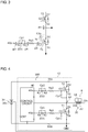
- Fig. 3 illustrates the operation of the switching device 100.
- a description will be given here of a case of switching from the initial first state (the lower switching element T1 is on, and the upper switching element T2 is off) to the second state (the lower switching element T1 is off, and the upper switching element T2 is on).
- the switching is performed in response to a change in an input signal to an input part CNT of the control circuit 40.
- the first output part 40p of the control circuit 40 outputs a high level, and the second output part 40s outputs a low level.
- the first output part 40p is at a high level, a voltage lower by the Zener voltage Vz than the high level potential is applied to the gate G1 of the lower switching element T1. In this process, the charge commensurate with the Zener voltage Vz is stored in the parallel capacitor Cp1.
- the second output part 40s is at a low level, substantially 0 V is applied to the gate G2, and the upper switching element T2 is off.
- the first output part 40p of the control circuit 40 changes to a low level
- the second output part 40s changes to a high level
- a voltage lower by the Zener voltage Vz than the high level potential is applied to the gate G2 of the upper switching element T2, and the upper switching element T2 is turned on.
- the upper switching element T2 is turned on, the potential at the drain D1 as well as the source S2 rises abruptly, as indicated by an arrow p1.
- a current ig is injected to the gate G1 of the lower switching element T1 via the drain-gate parasitic capacitance Cdg.
- the parallel capacitor Cp1 operates as a negative voltage generating circuit and prohibits self turn-on by absorbing the injected current.
- the parallel capacitor Cp1 and the Zener diode ZD1 prevent self turn-on of the lower switching element T1 from occurring even when the current ig is injected via the parasitic capacitance Cdg, allowing the lower switching element T1 to be turned off in a short period of time. As the lower switching element T1 is turned off, the second state is induced.
- the second output part 40s of the control circuit 40 outputs a high level, and the first output part 40p outputs a low level.
- the second output part 40s is at a high level, a voltage lower by the Zener voltage Vz than the high level potential is applied to the gate G2 of the upper switching element T2. In this process, the charge commensurate with the Zener voltage Vz is stored in the parallel capacitor Cp2 .
- the first output part 40p is at a low level, substantially 0 V is applied to the gate G1, and the lower switching element T1 is off.
- the second output part 40s of the control circuit 40 changes to a low level, and the first output part 40p changes to a high level.
- a voltage by the Zener voltage Vz lower than the high level potential is applied to the gate G1 of the lower switching element T1, and the lower switching element T1 is turned on.
- the lower switching element T1 is turned on, the potential at the source S2 as well as the drain D1 drops abruptly.
- the potential at the source S2 drops, a current is injected to the gate G2 of the upper switching element T2 via the drain-gate parasitic capacitance.
- the parallel capacitor Cp2 operates as a negative voltage generating circuit and prohibits self turn-on by absorbing the injected current.
- the side of the parallel capacitor Cp2 toward the second output part 40s is shifted to substantially 0 V, and the side of the parallel capacitor Cp2 toward the gate resistor Rg2 is shifted to a voltage (negative voltage) lower by the Zener voltage Vz than 0 V.
- the negative voltage is applied to the gate G2 of the upper switching element T2.
- the parallel capacitor Cp2 and the Zener diode ZD2 prevent self turn-on of the upper switching element T2 from occurring even when a current is injected via the parasitic capacitance, allowing the upper switching element T2 to be turned off in a short period of time. As the upper switching element T2 is turned off, the first state is induced.
- the negative voltage generating function of the parallel capacitor and the Zener diode prevents self turn-on of the switching elements in a transition between the first state and the second state.
- the Zener voltage Vz of the Zener diodes ZD1, ZD2 is set to restrict excessive drop of the gate potential in this embodiment.
- the Zener voltage Vz may be set to be lower than a permitted value of the gate-source voltage Vgs of the switching elements T1, T2 in the negative direction (the value permitted in the case the gate potential is negative relative to the source potential.
- the permitted value of the voltage Vgs in the negative direction is 5 V
- the Zener voltage Vz is set to 3 V.
- the capacitance of the gate-side capacitors Cg1, Cg2 is set to be lower than the parallel capacitors Cp1, Cp2 in this embodiment.
- the capacitance of the parallel capacitors Cp1, Cp2 may be set to be in a range of 500 times-2000 times the capacitance of the gate-side capacitors Cg1, Cg2.
- a switching device 100 includes: a lower switching element T1, a drain of the lower switching element outputting a switch driving signal; an upper switching element T2 having a source S2 connected to the drain D1 of the lower switching element T1; a control circuit 40 including a first output part 40p that supplies a driving signal to the lower switching element T1; a Zener diode ZD1 having a cathode K1 connected to the first output part 40p; a parallel capacitor Cp1 connected to the Zener diode ZD1 in parallel; a gate resistor Rg1 connected between an anode A1 of the Zener diode ZD1 and a gate G1 of the lower switching element T1; and a gate-side capacitor Cg1 connected between the gate G1 and a source S1 of the lower switching element T1.
- the control circuit may include a second output part 40s that supplies a driving signal to the upper switching element T2, and the switching device may further include: a further Zener diode ZD2 having a cathode K2 connected to the second output part 40s; a further parallel capacitor Cp2 connected to the further Zener diode ZD2 in parallel; a further resistor Rg2 connected between an anode A2 of the further Zener diode ZD2 and a gate G2 of the upper switching element T2; and a further gate-side capacitor Cg2 connected, outside the upper switching element T2, between the gate G2 and the source S2 of the upper switching element T2.
- a further Zener diode ZD2 having a cathode K2 connected to the second output part 40s
- a further parallel capacitor Cp2 connected to the further Zener diode ZD2 in parallel
- a further resistor Rg2 connected between an anode A2 of the further Zener diode ZD2 and a gate G2 of the
- the lower switching element T1 and the upper switching element T2 may be SiC-MOSFETs or GaN-MOSFETs. In this case, it is possible to inhibit an increase in the loss occurring when the switching elements are switched at a high speed.
- a Zener voltage of the Zener diode ZD1 may be set to be lower than a permitted value of a gate-source voltage of the lower switching element T1 in a negative direction. In this case, it is possible to prevent a voltage in excess of the permitted value from being applied to the lower switching element T1 and to prevent a fault of the switching element.
- the capacitance of the gate-side capacitor Cg1 may be smaller than a capacitance of the parallel capacitor Cp1. In this case, it is possible to inhibit the switching speed of the lower switching element T1 from being lowered.
- FIG. 4 is a block diagram showing an example of the driving circuit device 10 for actuators.
- constituting elements and members identical or equivalent to those of the first embodiment shall be denoted by the same reference numerals. Duplicative explanations are omitted appropriately and features different from those of the first embodiment will be highlighted.
- the driving circuit device 10 includes the switching device 100 according to the first embodiment and drives an actuator 8.
- the actuator 8 is a linear motor including a stator 20 having a one-phase armature coil 22, and a movable part 18 capable of linear motion relative to the stator 20.
- This embodiment is provided with the switching device 100 for driving one end 22a of the armature coil 22.
- the other end 22b of the armature coil 22 is connected to a midpoint 30c of the DC power supply unit 30.
- the actuator 8 may be a linear motor of voice coil type.
- the switching device 100 subjects the coil 22 to switch driving based on the switching signal. This induces a driving current in the coil 22 and supplies a driving magnetic field to the movable part 18.
- the movable part 18 outputs a driving force in accordance with the driving magnetic field.
- This embodiment provide the same advantage and benefit as the first embodiment.
- FIG. 5 is a block diagram showing an example of the actuator system 1.
- constituting elements and members identical or equivalent to those of the first embodiment shall be denoted by the same reference numerals. Duplicative explanations are omitted appropriately and features different from those of the first embodiment will be highlighted.
- the actuator system 1 includes the switching devices100 according to the first embodiment, the stator 20 having the armature coil 22, and the movable part 18 provided such that rotational motion or linear motion relative to the stator 20 is possible.
- the movable part 18 and the stator 20 constitute an actuator.
- the plurality of switching devices 100 are discriminated from each other by appending "-U", “-V", “-W" at the end of the reference numerals.
- the stator 20 includes a three-phase armature coil 22.
- the armature coil 22 includes three coils 22u, 22v, 22w in three-phase star connection.
- This embodiment includes three sets of switching devices 100-U, 100-V, 100-W that drive the three coils 22u, 22v, 22w, respectively.
- the movable part 18 may be a rotor wrapped around the stator 20 via a magnetic gap (not shown) .By way of one example, the movable part 18 and the stator 20 may be an interior permanent magnet (IPM) motor.
- IPM interior permanent magnet
- This embodiment provide the same advantage and benefit as the first embodiment.
- FIG. 6 is a block diagram showing the switching device 200 according to the first variation and corresponds to Fig. 1 .
- the switching device 200 according to the first variation differs from the first embodiment in that Miller clamp switching elements T3, T4 are provided in place of the gate-side capacitors Cg1, Cg2, and the other features are analogous to each other. Therefore, the switching elements T3, T4 will be described mainly.
- the Miller clamp switching elements T3, T4 are provided in place of the gate-side capacitors Cg1, Cg2.
- the control circuit 40 lowers the potential at the gates G1, G2 of the switching elements T1, T2 by turning the Miller clamp switching elements T3, T4 on, respectively.
- drains D3, D4 of the switching elements T3, T4 are connected to the gates G1, G2 of the switching elements T1, T2, respectively.
- Sources S3, S4 of the switching elements T3, T4 are connected to the ground line GND.
- the sources S3, S4 of the switching elements T3, T4 may be connected to the sources S1, S2 of the switching elements T1, T2, respectively.
- the control circuit 40 includes an inverted output part 40q that supplies an inverted version of a first driving signal to the gate G3 of the switching element T3 and an inverted output part 40r that supplies an inverted version of a second driving signal to the gate G4 of the switching element T4.
- the inverted output parts 40q, 40r output inverted versions of the output signals of the first and second output parts 40p, 40s, respectively.
- the inverted output parts 40q, 40r output a low level.
- the inverted output parts 40q, 40r output a high level.
- the switching elements T3, T4 are turned on. The drains D3, D4 bypass the gate resistors Rg1, Rg2, lowering the potential at the gates G1, G2 positively and preventing self turn-on of the switching elements T1, T2, respectively.
- the switching elements T3, T4 may be of the same type as the switching element T1, T2 or may be of a different type.
- the switching elements T3, T4 according to this variation are n-channel MOSFETs having a current capacity smaller than that of the switching elements T1, T2.
- a low speed of the switching elements T3, T4 results in poor self turn-on prevention performance.
- SiC-MOSFET or GaN-MOSFET capable of high-speed operation are employed for the switching elements T3, T4 according to this variation.
- the further Zener diode ZD2 may be omitted.
- the first variation provides the same advantage and benefit as the first embodiment.
- a further advantage of the first variation is that reduction in the speed of the switching elements T1, T2 due to the gate-side capacitors Cg1, Cg2 hardly occurs so that the switching loss is reduced.
- the turn-on delay time of the switching elements T3, T4 may be shorter than the turn-on delay time of the switching elements T1, T2 from the perspective of lowering the potential at the gates G1, G2 of the switching elements T1, T2 promptly.
- the turn-on delay time of the switching elements T3, T4 may be preferably 50% or shorter, and, more preferably, 30% or shorter, and, still more preferably, 20% or shorter than the turn-on delay time of the switching elements T1, T2.
- FIG. 7 is a block diagram showing the switching device 300 according to the second variation and corresponds to Fig. 1 .
- the switching device 300 according to the second variation differs from the first embodiment in that the device includes a parallel Zener diode ZD3 connected to the Zener diode ZD1 in parallel such that the cathodes thereof are connected to each other and includes and a parallel Zener diode ZD4 connected to the Zener diode ZD2 in parallel such that the cathodes thereof are connected to each other.
- the other features are analogous to each other. Therefore, the parallel Zener diodes ZD3, ZD4 will be described mainly.
- anodes A3, A4 of the parallel Zener diodes ZD3, ZD4 are connected to the anodes A1, A2 of the Zener diodes ZD1, ZD2, respectively, and cathodes K3, K4 of the parallel Zener diodes ZD3, ZD4 are connected to the cathodes K1, K2 of the Zener diodes ZD1, ZD2, respectively.
- the parallel Zener diode ZD3 operates in the same manner as the Zener diode ZD1
- the parallel Zener diode ZD4 operates in the same manner as the Zener diode ZD2.
- the second variation provides the same advantage and benefit as the first embodiment.
- a further advantage of the second variation is that, when an open fault of one of the Zener diodes ZD1 and the parallel Zener diode ZD3 occurs, the other fulfils the function. Similarly, when an open fault occurs in one of the Zener diode ZD2 and the parallel Zener diode D4 occurs, the other fulfils the function. By causing one to back up the other in the event of a fault, the switching device 300 can be made redundant.
- the Zener voltage of the parallel Zener diode ZD3 may be set to be higher than the Zener voltage of the Zener diode ZD1.
- the Zener voltage of the parallel Zener diode ZD3 may be set to be higher by 1 V or more than the Zener voltage of the Zener diode ZD1.
- Zener voltage of the parallel Zener diode ZD3 is preferably 3 V or smaller, and, more preferably, 2 V or smaller.
- the Zener voltage of the parallel Zener diode ZD4 may be set to be higher by 1 V or more than the Zener voltage of the Zener diode ZD2.
- the difference between the Zener voltage of the parallel Zener diode ZD4 and the Zener voltage of the Zener diode ZD2 is preferably 3 V or smaller, and, more preferably, 2 V or smaller.
- the switching elements T1-T4 are described as being n-channel MOSFETs.
- the switching elements may be p-channel MOSFETs.
- the switching device 100 is described as being driven by a single power supply. Alternatively, the switching device 100 may be driven by a dual power supply.
- the plurality of switching devices 100 are described as being controlled by a plurality of independent control circuits 40.
- the plurality of switching devices may be controlled by a single control circuit.
Landscapes
- Engineering & Computer Science (AREA)
- Physics & Mathematics (AREA)
- Power Engineering (AREA)
- Electromagnetism (AREA)
- General Physics & Mathematics (AREA)
- Radar, Positioning & Navigation (AREA)
- Automation & Control Theory (AREA)
- Nonlinear Science (AREA)
- Electronic Switches (AREA)
- Power Conversion In General (AREA)
- Inverter Devices (AREA)
Abstract
Description
- The present invention relates to a switching device, a driving circuit device for actuators, and an actuator system.
- Devices provided with a totem-pole switching circuit are known. The circuit includes an upper arm switching element and a lower arm switching element connected vertically. For example,
patent literature 1 discloses an inverter circuit for subjecting a three-phase coil of an electric motor to PWM driving. The inverter circuit includes a tote-pole circuit that combines an upper arm switching element and a lower arm switching element. The circuit is provided with a bootstrap circuit that turns on the upper arm switching element by using a capacitor. - [Patent literature 1]
JP-2018-064322 - We have gained the following recognition about devices provided with a switching circuit. In the case of a totem-pole switching circuit having upper and lower switching elements, one should be mindful of occurrence of parasitic turn-on caused by parasitic capacitance or floating capacitance. When the upper switching element is turned on while the lower switching element is off, for example, the gate potential of the lower switching element increases via the parasitic capacitance. When the gate potential exceeds a threshold value, the lower switching element is turned on (hereinafter, called "self turn-on"), causing a short-circuit current to flow in the upper and lower switching elements.
- To reduce the switching loss of switching elements, it is conceivable to employ a switching element capable of high-speed switching. A problem with the use of a high-speed switching element is that the lower switching element is turned on in a short period of time since the gate potential increases so that a short circuit of the upper and lower switching elements due to self turn-on occurs easily.
- Based on the foregoing, we have realized that there is room for improvement in devices provided with a switching circuit from the perspective of reducing the occurrence of self turn-on.
- The present invention addresses the above-described issue, and a general purpose thereof is to provide a switching device capable of inhibiting self turn-on.
- A switching device according to an embodiment of the present invention includes: a lower switching element, a drain of the lower switching element outputting a switch driving signal; an upper switching element having a source connected to the drain of the lower switching element; a control circuit including an output part that supplies a driving signal to the lower switching element; a Zener diode having a cathode connected to the output part; a parallel capacitor connected to the Zener diode in parallel; a resistor connected between an anode of the Zener diode and a gate of the lower switching element; and a gate-side capacitor provided separate from a parasitic capacitance of the lower switching element, having a larger capacitance than the parasitic capacitance of the lower switching element, and connected, outside the lower switching element, between the gate and a source of the lower switching element. The capacitance of the gate-side capacitor is smaller than a capacitance of the parallel capacitor.
- Optional combinations of the aforementioned and replacement of constituting elements or implementation of the present invention in the form of methods, devices, programs, transitory or non-transitory recording mediums storing programs, systems, etc. may also be practiced as optional modes of the present invention.
-
Fig. 1 is a block diagram showing an example of the switching device according to the first embodiment of the present invention; -
Fig. 2 illustrates self turn-on of the switching device according to a comparative example; -
Fig. 3 illustrates the operation of the switching device ofFig. 1 ; -
Fig. 4 is a block diagram showing an example of the driving circuit device for actuators according to the second embodiment of the present invention; -
Fig. 5 is a block diagram showing an example of the actuator system according to the third embodiment of the present invention; -
Fig. 6 is a block diagram showing the switching device according to the first variation; and -
Fig. 7 is a block diagram showing the switching device according to the second variation. - The invention will now be described by reference to the preferred embodiments. This does not intend to limit the scope of the present invention, but to exemplify the invention.
- The present invention will be described based on preferred embodiments with reference to the drawings. In the embodiments and variations, the same or equivalent constituting elements and members shall be denoted by the same reference numerals, and duplicative explanations will be omitted appropriately. The dimension of members in the drawings shall be enlarged or reduced as appropriate to facilitate understanding. Those of the members that are not material to the description of the embodiments are omitted in the drawings.
- Terms including ordinal numbers like first and second are used to describe a variety of constituting elements, but those terms are used solely for the purpose of distinguishing one constituting element from another and shall not limit the constituting elements.
- A description will be given of a configuration of a
switching device 100 according to the first embodiment of the present invention with reference to the drawings. Theswitching device 100 is suitably used to subject a driven object such as an electric actuator to switch driving. In particular, theswitching device 100 could be used to subject an actuator for airplanes, for which high reliability is required, to switch driving.Fig. 1 is a block diagram showing an example of theswitching device 100 according to the first embodiment. Theswitching device 100 outputs a switch driving signal from an output end Sp to subject a load (e.g., a coil of an actuator) connected to the output end Sp to switch driving. - The
switching device 100 mainly includes a lower switching element T1, an upper switching element T2, acontrol circuit 40, Zener diodes ZD1, ZD2, parallel capacitors Cp1, Cp2, gate resistors Rg1, Rg2, and gate-side capacitors Cg1, Cg2. Generically, the lower switching element T1 and the upper switching element T2 are simply referred to as switching elements . The switching element may be of any type so long as it is a semiconductor switching element capable of controlling the drain-source conduction state according to the gate voltage. - From the perspective of reducing a switching loss, a silicon carbide-metal-oxide-semiconductor field-effect transistor (SiC-MOSFET) or a gallium nitride-metal-oxide-semiconductor field-effect transistor (GaN-MOSFET) is employed as the switching element of this embodiment. The switching element of
Fig. 1 is an n-channel MOSFET. Therefore, the switching element is turned on when the gate voltage is higher than a threshold value and is turned off when the gate voltage is lower than the threshold value. - The lower switching element T1 and the upper switching element T2 have gates G1, G2, sources S1, S2, and drains D1, D2, respectively. The drain D1 of the lower switching element T1 and the source S2 of the upper switching element T2 are connected to each other to form the output end Sp. The source S1 of the lower switching element T1 is connected to a
negative side 30m of a DCpower supply unit 30. The drain D2 of the upper switching element T2 is connected to apositive side 30p of the DCpower supply unit 30. Thenegative side 30m is so referred to, to mean that the side is negative with respect to thepositive side 30p. In the illustrated example ofFig. 1 , thenegative side 30m is connected to the ground line GND of theswitching device 100. The potential of the ground line GND is 0 V. Generically, the gates G1, G2, the source S1, S2, and the drains D1, D2 are simply referred to as gates, sources, and drains. - The
control circuit 40 functions as gate driver for outputting a driving signal to the switching elements based on an input signal from a superior system input to an input part CTN. Thecontrol circuit 40 according to this embodiment includes afirst output part 40p that supplies a driving signal to the lower switching element T1 and asecond output part 40s that supplies a driving signal to the upper switching element T2. Generically, the first andsecond output parts - The Zener diode ZD1 has a cathode K1 and an anode A1. The cathode K1 of the Zener diode ZD1 is connected to the
first output part 40p, and the anode A1 is connected to one end of the gate resistor Rg1. The Zener diode ZD2 has a cathode K2 and an anode A2. The cathode K2 of the Zener diode ZD2 is connected to thesecond output part 40s, and the anode A2 is connected to one end of the gate resistor Rgs. For example, the Zener voltage Vz of the Zener diodes ZD1, ZD2 may be set in a range of not lower than 1 V and not higher than 5 V. - In this embodiment, no series resistors or parallel resistors are connected to the Zener diodes ZD1, ZD2. The anodes A1, A2 and the cathodes K1, K2 are directly connected to the ends of the parallel capacitors Cp1, Cp2, respectively. In this embodiment, no series resistors or parallel resistors are connected to the parallel capacitors Cp1, Cp2. The ends of the parallel capacitors Cp1, Cp2 are directly connected to the anodes A1, A2 and the cathodes K1, K2, respectively.
- The parallel capacitor Cp1 is connected to the Zener diode ZD1 in parallel. The parallel capacitor Cp2 is connected to the Zener diode ZD2 in parallel. The parallel capacitors Cp1, Cp2 operate as a negative voltage generating circuit that generates a negative voltage on the anode side. The Zener diodes ZD1, ZD2 transmit a driving signal of the output part to the gate and clamps the voltage across the parallel capacitors Cp1, Cp2, respectively. Generically, the parallel capacitors Cp1, Cp2 and the Zener diode ZD1 are simply referred to as parallel capacitors and Zener diodes. For example, the capacitance of the parallel capacitors Cp1, Cp2 may be set to a range of not larger than 3 µF. In particular, the capacitance of the parallel capacitors Cp1, C2 is preferably equal to or larger than 0.5 µF, and, more preferably, equal to or larger than 1 µF, and, still more preferably, equal to or larger than 2 µF.
- The gate resistor Rg1 is connected between the anode A1 of the Zener diode ZD1 and the gate G1 of the lower switching element T1. The gate resistor Rg2 is connected between the anode A2 of the Zener diode ZD2 and the gate G2 of the upper switching element T2. Generically, the gate resistor Rg1 and the gate resistor Rg2 are simply referred to as gate resistors. The gate resistor can adjust the switching speed of the switching element. The larger the gate resistance, the lower the switching speed, and the smaller the gate resistance, the higher the switching speed. For example, the resistance value of the gate resistors Rg1, Rg2 may be set to be 200 Ω or smaller. In particular, the resistance value of the gate resistors Rg1, Rg2 is preferably 10 Ω or larger, and, more preferably, 30 Ω or larger, and, still more preferably, 100 Ω or larger.
- The gate-side capacitor Cg1 is connected between the gate G1 and the source S1 of the lower switching element T1. The gate-side capacitor Cg1 is provided outside the lower switching element T1 apart from the gate G1-source S1 parasitic capacitance inside the lower switching element T1. The capacitance of the gate-side capacitor Cg1 may be larger than the gate G1-source S1 parasitic capacitance. In particular, the capacitance of the gate-side capacitor Cg1 is preferably 10 times or larger, and, more preferably, 100 times or larger, and, still more preferably, 1000 times or larger than the gate G1-source S1 parasitic capacitance.
- The gate-side capacitor Cg2 is connected between the gate G2 and the source S2 of the upper switching element T2. The gate-side capacitor Cg2 is provided outside the upper switching element T2 apart from the gate G2-source S2 parasitic capacitance inside the upper switching element T2. The capacitance of the gate-side capacitor Cg2 may be larger than the gate G2-source S2 parasitic capacitance. In particular, the capacitance of the gate-side capacitor Cg2 is preferably 10 times or larger, and, more preferably, 100 times or larger, and, still more preferably, 1000 times or larger than the gate G2-source S2 parasitic capacitance.
- Generically, the gate-side capacitors Cg1, Cg2 are referred to as gate-side capacitors. The gate-side capacitor absorbs the current flowing into the gate due to the parasitic capacitance and inhibits an increase in the gate voltage. The capacitance of the gate-side capacitor may be set to be larger than the parasitic capacitance. For example, the capacitance of the gate-side capacitors Cg1, Cg2 may be set in a range of not larger than 2000 PF. In particular, the capacitance of the gate-side capacitors Cg1, Cg2 is preferably 500 PF or larger, and, more preferably, 1000 PF or larger.
- The time constant defined by the gate resistor Rg1 and the gate-side capacitor Cg1 is preferably 5 ns or longer, and, more preferably, 15 ns or longer, and, still more preferably, 50 ns or longer. The time constant defined by the gate resistor Rg2 and the gate-side capacitor Cgs is preferably 5 ns or longer, and, more preferably, 15 ns or longer, and, still more preferably, 50 ns or longer.
- A description will now be given, with reference also to
Fig. 2 , of self turn-on in a comparative example in which the parallel capacitor Cp1 and the Zener diode ZD1 are removed.Fig. 2 illustrates self turn-on in a comparative example. When thesecond output part 40s goes to a high level, the upper switching element T2 is turned on, and the potential at the drain D1 as well as the source S2 rises abruptly, as indicated by an arrow p1. When the potential at the drain D1 rises, a current ig is injected to the gate G1 of the lower switching element T1 via a drain-source parasitic capacitance Cdg of the lower switching element T1. When the current ig is injected, the potential at the gate G1 rises, as indicated by an arrow p2. When the potential at the gate G1 exceeds a threshold value, the lower switching element T1 undergoes self turn-on, and a short circuit current flows in the upper and lower switching elements. - Based on the description of the comparative example, the operation according to this embodiment will be described. Reference is also made to
Fig. 3. Fig. 3 illustrates the operation of theswitching device 100. A description will be given here of a case of switching from the initial first state (the lower switching element T1 is on, and the upper switching element T2 is off) to the second state (the lower switching element T1 is off, and the upper switching element T2 is on). The switching is performed in response to a change in an input signal to an input part CNT of thecontrol circuit 40. - In the first state, the
first output part 40p of thecontrol circuit 40 outputs a high level, and thesecond output part 40s outputs a low level. When thefirst output part 40p is at a high level, a voltage lower by the Zener voltage Vz than the high level potential is applied to the gate G1 of the lower switching element T1. In this process, the charge commensurate with the Zener voltage Vz is stored in the parallel capacitor Cp1. When thesecond output part 40s is at a low level, substantially 0 V is applied to the gate G2, and the upper switching element T2 is off. - When an input signal for switching to the second state is input to the
control circuit 40, thefirst output part 40p of thecontrol circuit 40 changes to a low level, and thesecond output part 40s changes to a high level. When thesecond output part 40s changes to a high level, a voltage lower by the Zener voltage Vz than the high level potential is applied to the gate G2 of the upper switching element T2, and the upper switching element T2 is turned on. When the upper switching element T2 is turned on, the potential at the drain D1 as well as the source S2 rises abruptly, as indicated by an arrow p1. When the potential at the drain D1 rises, a current ig is injected to the gate G1 of the lower switching element T1 via the drain-gate parasitic capacitance Cdg. However, the parallel capacitor Cp1 operates as a negative voltage generating circuit and prohibits self turn-on by absorbing the injected current. - A description will be given of the negative voltage generating circuit. When the
first output part 40p changes to a low level as indicated by an arrow p3, the side of the parallel capacitor Cp1 toward thefirst output part 40p is shifted to substantially 0 V. In this process, the side of the parallel capacitor Cp1 toward the gate resistor Rg1 is shifted to a voltage (negative voltage) lower by the Zener voltage Vz than 0 V, as indicated by an arrow p4. As a result, the negative voltage is applied to the gate G1 of the lower switching element T1 as indicated by an arrow p5. In other words, the parallel capacitor Cp1 and the Zener diode ZD1 prevent self turn-on of the lower switching element T1 from occurring even when the current ig is injected via the parasitic capacitance Cdg, allowing the lower switching element T1 to be turned off in a short period of time. As the lower switching element T1 is turned off, the second state is induced. - A description will now be given of a case of switching from the second state to the first state. The switching is performed in response to a change in an input signal to the input part CNT of the
control circuit 40. - In the second state, the
second output part 40s of thecontrol circuit 40 outputs a high level, and thefirst output part 40p outputs a low level. When thesecond output part 40s is at a high level, a voltage lower by the Zener voltage Vz than the high level potential is applied to the gate G2 of the upper switching element T2. In this process, the charge commensurate with the Zener voltage Vz is stored in the parallel capacitor Cp2 . When thefirst output part 40p is at a low level, substantially 0 V is applied to the gate G1, and the lower switching element T1 is off. - When an input signal for switching from the second state to the first state is input to the input part CNT, the
second output part 40s of thecontrol circuit 40 changes to a low level, and thefirst output part 40p changes to a high level. When thefirst output part 40p changes to a high level, a voltage by the Zener voltage Vz lower than the high level potential is applied to the gate G1 of the lower switching element T1, and the lower switching element T1 is turned on. When the lower switching element T1 is turned on, the potential at the source S2 as well as the drain D1 drops abruptly. When the potential at the source S2 drops, a current is injected to the gate G2 of the upper switching element T2 via the drain-gate parasitic capacitance. However, the parallel capacitor Cp2 operates as a negative voltage generating circuit and prohibits self turn-on by absorbing the injected current. - When the
second output part 40s changes to a low level, the side of the parallel capacitor Cp2 toward thesecond output part 40s is shifted to substantially 0 V, and the side of the parallel capacitor Cp2 toward the gate resistor Rg2 is shifted to a voltage (negative voltage) lower by the Zener voltage Vz than 0 V. As a result, the negative voltage is applied to the gate G2 of the upper switching element T2. In other words, the parallel capacitor Cp2 and the Zener diode ZD2 prevent self turn-on of the upper switching element T2 from occurring even when a current is injected via the parasitic capacitance, allowing the upper switching element T2 to be turned off in a short period of time. As the upper switching element T2 is turned off, the first state is induced. - Thus, the negative voltage generating function of the parallel capacitor and the Zener diode prevents self turn-on of the switching elements in a transition between the first state and the second state.
- A further description of the Zener diode will be given. When the gate potential of the switching element drops excessively relative to the source potential, the switching element may be damaged, and a fault may occur. For this reason, the Zener voltage Vz of the Zener diodes ZD1, ZD2 is set to restrict excessive drop of the gate potential in this embodiment. In particular, the Zener voltage Vz may be set to be lower than a permitted value of the gate-source voltage Vgs of the switching elements T1, T2 in the negative direction (the value permitted in the case the gate potential is negative relative to the source potential. In this example, the permitted value of the voltage Vgs in the negative direction is 5 V, and the Zener voltage Vz is set to 3 V.
- A further description will be given of the gate-side capacitors Cg1, Cg2. If the capacitance of the gate-side capacitors Cg1, Cg2 is too large, the switching speed of the switching elements T1, T2 is lowered. For this reason, the capacitance of the gate-side capacitors Cg1, Cg2 is set to be lower than the parallel capacitors Cp1, Cp2 in this embodiment. For example, the capacitance of the parallel capacitors Cp1, Cp2 may be set to be in a range of 500 times-2000 times the capacitance of the gate-side capacitors Cg1, Cg2.
- A description will now be given of the features of the
switching device 100 according to the first embodiment. - A
switching device 100 includes: a lower switching element T1, a drain of the lower switching element outputting a switch driving signal; an upper switching element T2 having a source S2 connected to the drain D1 of the lower switching element T1; acontrol circuit 40 including afirst output part 40p that supplies a driving signal to the lower switching element T1; a Zener diode ZD1 having a cathode K1 connected to thefirst output part 40p; a parallel capacitor Cp1 connected to the Zener diode ZD1 in parallel; a gate resistor Rg1 connected between an anode A1 of the Zener diode ZD1 and a gate G1 of the lower switching element T1; and a gate-side capacitor Cg1 connected between the gate G1 and a source S1 of the lower switching element T1. - According to this configuration, it is possible to prevent self turn-on of the lower switching element T1 caused by the parasitic capacitance or the floating capacitance and to avoid a short circuit due to simultaneous turn-on of the upper and lower switching elements T2 and T1.
- The control circuit may include a
second output part 40s that supplies a driving signal to the upper switching element T2, and the switching device may further include: a further Zener diode ZD2 having a cathode K2 connected to thesecond output part 40s; a further parallel capacitor Cp2 connected to the further Zener diode ZD2 in parallel; a further resistor Rg2 connected between an anode A2 of the further Zener diode ZD2 and a gate G2 of the upper switching element T2; and a further gate-side capacitor Cg2 connected, outside the upper switching element T2, between the gate G2 and the source S2 of the upper switching element T2. In this case, it is possible to prevent self turn-on of the upper switching element T2 caused by the parasitic capacitance or the floating capacitance and to avoid a short circuit due to simultaneous turn-on of the upper and lower switching elements T2 and T1. - The lower switching element T1 and the upper switching element T2 may be SiC-MOSFETs or GaN-MOSFETs. In this case, it is possible to inhibit an increase in the loss occurring when the switching elements are switched at a high speed.
- A Zener voltage of the Zener diode ZD1 may be set to be lower than a permitted value of a gate-source voltage of the lower switching element T1 in a negative direction. In this case, it is possible to prevent a voltage in excess of the permitted value from being applied to the lower switching element T1 and to prevent a fault of the switching element.
- The capacitance of the gate-side capacitor Cg1 may be smaller than a capacitance of the parallel capacitor Cp1. In this case, it is possible to inhibit the switching speed of the lower switching element T1 from being lowered.
- A description will now be given of a
driving circuit device 10 for actuators according to the second embodiment of the present invention.Fig. 4 is a block diagram showing an example of the drivingcircuit device 10 for actuators. In the drawing and description of the second embodiment, constituting elements and members identical or equivalent to those of the first embodiment shall be denoted by the same reference numerals. Duplicative explanations are omitted appropriately and features different from those of the first embodiment will be highlighted. - The driving
circuit device 10 includes theswitching device 100 according to the first embodiment and drives anactuator 8. In the example ofFig. 4 , theactuator 8 is a linear motor including astator 20 having a one-phase armature coil 22, and amovable part 18 capable of linear motion relative to thestator 20. This embodiment is provided with theswitching device 100 for driving oneend 22a of thearmature coil 22. Theother end 22b of thearmature coil 22 is connected to amidpoint 30c of the DCpower supply unit 30. By way of one example, theactuator 8 may be a linear motor of voice coil type. - A description will be given of the operation. When a switching signal is input to the input part CNT of the
control circuit 40, theswitching device 100 subjects thecoil 22 to switch driving based on the switching signal. This induces a driving current in thecoil 22 and supplies a driving magnetic field to themovable part 18. Themovable part 18 outputs a driving force in accordance with the driving magnetic field. - This embodiment provide the same advantage and benefit as the first embodiment.
- A description will now be given of an
actuator system 1 according to the third embodiment of the present invention.Fig. 5 is a block diagram showing an example of theactuator system 1. In the drawing and description of the third embodiment, constituting elements and members identical or equivalent to those of the first embodiment shall be denoted by the same reference numerals. Duplicative explanations are omitted appropriately and features different from those of the first embodiment will be highlighted. - The
actuator system 1 includes the switching devices100 according to the first embodiment, thestator 20 having thearmature coil 22, and themovable part 18 provided such that rotational motion or linear motion relative to thestator 20 is possible. Themovable part 18 and thestator 20 constitute an actuator. InFig. 5 , the plurality of switchingdevices 100 are discriminated from each other by appending "-U", "-V", "-W" at the end of the reference numerals. - In the example of
Fig. 5 , thestator 20 includes a three-phase armature coil 22. Thearmature coil 22 includes threecoils coils movable part 18 may be a rotor wrapped around thestator 20 via a magnetic gap (not shown) .By way of one example, themovable part 18 and thestator 20 may be an interior permanent magnet (IPM) motor. - A description will now be given of the operation. When a switching signal for three-phase driving is input to input parts CNT-U, CNT-V, CNT-W of the
control circuit 40, the switching devices 100-U, 100-V, 100-W subject thecoils coils movable part 18 outputs a driving force in accordance with the driving magnetic field. - This embodiment provide the same advantage and benefit as the first embodiment.
- Exemplary embodiments of the present invention are described above in detail. The embodiments described above are merely specific examples of practicing the present invention. The details of the embodiments shall not be construed as limiting the technical scope of the present invention. A number of design modifications such as modification, addition, deletion, etc. of constituting elements may be made to the extent that they do not depart from the idea of the invention defined by the claims. Although the details subject to such design modification are emphasized in the embodiments by using phrases such as "of this embodiment" and "in this embodiment", details not referred to as such are also subject to design modification.
- A description will now be given of variations. In the drawings and description of the variations, constituting elements and members identical or equivalent to those of the embodiments shall be denoted by the same reference numerals. Duplicative explanations are omitted appropriately and features different from those of the first embodiment will be highlighted.
- A description will be given of a configuration of a
switching device 200 according to the first variation based on the first embodiment.Fig. 6 is a block diagram showing theswitching device 200 according to the first variation and corresponds toFig. 1 . Theswitching device 200 according to the first variation differs from the first embodiment in that Miller clamp switching elements T3, T4 are provided in place of the gate-side capacitors Cg1, Cg2, and the other features are analogous to each other. Therefore, the switching elements T3, T4 will be described mainly. - In the first variation, the Miller clamp switching elements T3, T4 are provided in place of the gate-side capacitors Cg1, Cg2. To turn the switching elements T1, T2 off, the
control circuit 40 lowers the potential at the gates G1, G2 of the switching elements T1, T2 by turning the Miller clamp switching elements T3, T4 on, respectively. - In the example of
Fig. 6 , drains D3, D4 of the switching elements T3, T4 are connected to the gates G1, G2 of the switching elements T1, T2, respectively. Sources S3, S4 of the switching elements T3, T4 are connected to the ground line GND. The sources S3, S4 of the switching elements T3, T4 may be connected to the sources S1, S2 of the switching elements T1, T2, respectively. - The
control circuit 40 includes an inverted output part 40q that supplies an inverted version of a first driving signal to the gate G3 of the switching element T3 and an inverted output part 40r that supplies an inverted version of a second driving signal to the gate G4 of the switching element T4. - The inverted output parts 40q, 40r output inverted versions of the output signals of the first and
second output parts second output parts second output parts - The switching elements T3, T4 may be of the same type as the switching element T1, T2 or may be of a different type. The switching elements T3, T4 according to this variation are n-channel MOSFETs having a current capacity smaller than that of the switching elements T1, T2. A low speed of the switching elements T3, T4 results in poor self turn-on prevention performance. For this reason, SiC-MOSFET or GaN-MOSFET capable of high-speed operation are employed for the switching elements T3, T4 according to this variation. In the example of
Fig. 6 , the further Zener diode ZD2 may be omitted. - The first variation provides the same advantage and benefit as the first embodiment. A further advantage of the first variation is that reduction in the speed of the switching elements T1, T2 due to the gate-side capacitors Cg1, Cg2 hardly occurs so that the switching loss is reduced.
- In the first variation, the turn-on delay time of the switching elements T3, T4 may be shorter than the turn-on delay time of the switching elements T1, T2 from the perspective of lowering the potential at the gates G1, G2 of the switching elements T1, T2 promptly. In particular, the turn-on delay time of the switching elements T3, T4 may be preferably 50% or shorter, and, more preferably, 30% or shorter, and, still more preferably, 20% or shorter than the turn-on delay time of the switching elements T1, T2.
- A description will be given of a configuration of a
switching device 300 according to the second variation based on the first embodiment.Fig. 7 is a block diagram showing theswitching device 300 according to the second variation and corresponds toFig. 1 . Theswitching device 300 according to the second variation differs from the first embodiment in that the device includes a parallel Zener diode ZD3 connected to the Zener diode ZD1 in parallel such that the cathodes thereof are connected to each other and includes and a parallel Zener diode ZD4 connected to the Zener diode ZD2 in parallel such that the cathodes thereof are connected to each other. The other features are analogous to each other. Therefore, the parallel Zener diodes ZD3, ZD4 will be described mainly. - When an open fault of one of the Zener diodes ZD1, ZD2 occurs, the voltage of the parallel capacitor Cp1 or Cp2 is no longer restricted, which may apply an excessively low potential to the gate of the switching element, with the result that the switching element may be damaged, and a fault may occur. This is addressed in this variation by providing the parallel Zener diodes ZD3, ZD4. As shown in
Fig. 7 , anodes A3, A4 of the parallel Zener diodes ZD3, ZD4 are connected to the anodes A1, A2 of the Zener diodes ZD1, ZD2, respectively, and cathodes K3, K4 of the parallel Zener diodes ZD3, ZD4 are connected to the cathodes K1, K2 of the Zener diodes ZD1, ZD2, respectively. - In other words, the parallel Zener diode ZD3 operates in the same manner as the Zener diode ZD1, and the parallel Zener diode ZD4 operates in the same manner as the Zener diode ZD2.
- The second variation provides the same advantage and benefit as the first embodiment. A further advantage of the second variation is that, when an open fault of one of the Zener diodes ZD1 and the parallel Zener diode ZD3 occurs, the other fulfils the function. Similarly, when an open fault occurs in one of the Zener diode ZD2 and the parallel Zener diode D4 occurs, the other fulfils the function. By causing one to back up the other in the event of a fault, the
switching device 300 can be made redundant. - In the second variation, the Zener voltage of the parallel Zener diode ZD3 may be set to be higher than the Zener voltage of the Zener diode ZD1. By way of one example, the Zener voltage of the parallel Zener diode ZD3 may be set to be higher by 1 V or more than the Zener voltage of the Zener diode ZD1.
- When a failure does not occur in either of the diodes, the current flows in the Zener diode ZD1 having a relatively lower Zener voltage and does not substantially flow or rise in the parallel Zener diode ZD3, hardly causing degradation of the parallel Zener diode ZD3. For this reason, the parallel Zener diode ZD3, which is not substantially degraded, can back up in the event of a fault in the Zener diode ZD1.
- A concern with too large a Zener voltage of the parallel Zener diode ZD3 is that it cannot restrict the voltage of the parallel capacitor Cp1. In this respect, the difference between the Zener voltage of the parallel Zener diode ZD3 and the Zener voltage of the Zener diode ZD1 is preferably 3 V or smaller, and, more preferably, 2 V or smaller.
- The same discussion as set forth above for the Zener voltage of the parallel Zener diode ZD3 also applies to the Zener voltage of the parallel Zener diode ZD4. By way of one example, the Zener voltage of the parallel Zener diode ZD4 may be set to be higher by 1 V or more than the Zener voltage of the Zener diode ZD2. Further, the difference between the Zener voltage of the parallel Zener diode ZD4 and the Zener voltage of the Zener diode ZD2 is preferably 3 V or smaller, and, more preferably, 2 V or smaller.
- In the description of the first embodiment, the switching elements T1-T4 are described as being n-channel MOSFETs. Alternatively, the switching elements may be p-channel MOSFETs.
- In the description of the first embodiment, the
switching device 100 is described as being driven by a single power supply. Alternatively, theswitching device 100 may be driven by a dual power supply. - In the description of the third embodiment with reference to
Fig. 5 , the plurality of switchingdevices 100 are described as being controlled by a plurality ofindependent control circuits 40. Alternatively, the plurality of switching devices may be controlled by a single control circuit. - The variations described above provide the same advantage and benefit as the embodiments.
- Any combination of an embodiment and a variation described above will also be useful as an embodiment of the present invention. A new embodiment created by a combination will provide the combined advantages of the embodiment and the variation as combined.
Claims (9)
- A switching device (100, 200, 300) comprising:a lower switching element (T1), a drain (D1) of the lower switching element (T1) outputting a switch driving signal;an upper switching element (T2) having a source (S1) connected to the drain (D1) of the lower switching element (T1) ;a control circuit (40) including an output part (40p) that supplies a driving signal to the lower switching element (T1);a Zener diode (ZD1) having a cathode (K1) connected to the output part (40p);a parallel capacitor (Cp1) connected to the Zener diode (ZD1) in parallel;a resistor (Rg1) connected between an anode (A1) of the Zener diode (ZD) and a gate (G1) of the lower switching element (T1); anda gate-side capacitor (Cg1) provided separate from a parasitic capacitance of the lower switching element (T1), having a larger capacitance than the parasitic capacitance of the lower switching element (T1), and connected, outside the lower switching element (T1), between the gate (G1) and a source (S1) of the lower switching element (T1), whereinthe capacitance of the gate-side capacitor (Cg1) is smaller than a capacitance of the parallel capacitor (Cp1).
- The switching device (100, 200, 300) according to claim 1, wherein
the control circuit (40) includes a further output part (40s) that supplies a driving signal to the upper switching element (T2);
the switching device (100, 200, 300) further comprising:a further Zener diode (ZD) having a cathode (K) connected to the further output part (40s);a further parallel capacitor (Cp2) connected to the further Zener diode (ZD2) in parallel;a further resistor (Rg2) connected between an anode (A2) of the further Zener diode (ZD2) and a gate (G2) of the upper switching element (T2); anda further gate-side capacitor (Cg2) connected, outside the upper switching element (T2), between the gate (G2) and the source (S2) of the upper switching element (T2), whereina capacitance of the further gate-side capacitor (Cg2) is smaller than a capacitance of the further parallel capacitor (Cp2) . - The switching device (100, 200, 300) according to claim 2, wherein
the capacitance of the parallel capacitor (Cp1) is set to be in a range of 500 times-2000 times the capacitance of the gate-side capacitor (Cg1), and the capacitance of the further parallel capacitor (Cp2) is set to be in a range of 500 times-2000 times the capacitance of the further gate-side capacitor (Cg2). - The switching device (100, 200, 300) according to any one of claims 1 through 3, wherein
the lower switching element (T1) and the upper switching element (T2) are SiC-MOSFETs or GaN-MOSFETs. - The switching device (300) according to any one of claims 1 through 4, further comprising:
a parallel Zener diode (ZD3) connected to the Zener diode (ZD1) such that cathodes (K1,K3) of the Zener diode (ZD1) and the parallel Zener diode (ZD3) are connected to each other. - The switching device (100, 200, 300) according to any one of claims 1 through 5, wherein
a Zener voltage of the Zener diode (ZD1) is set to be lower than a permitted value of a gate-source voltage of the lower switching element (T1) in a negative direction. - The switching device (200) according to any one of claims 1 through 6, wherein
a Miller clamp switching element (T3) is provided in place of the gate-side capacitor (Cg1), and
to turn the lower switching element (T1) off, the control circuit (40) lowers a gate potential of the lower switching element (T1) by turning the Miller clamp switching element (T3) on. - A driving circuit device (10) comprising:an output end (Sp) connected to an armature coil (22) of an electric actuator (8);a lower switching element (T1) having a drain (D1) connected to the output end (Sp);an upper switching element (T2) having a source (S2) connected to the drain (D1) of the lower switching element (T1) ;a control circuit (40) including an output part (40p) that supplies a driving signal to the lower switching element (T1) and a further output part (40s) that supplies a driving signal to the upper switching element (T2);a Zener diode (ZD1) having a cathode (K1) connected to the output part (40p);a parallel capacitor (Cp1) connected to the Zener diode (ZD1) in parallel;a resistor (Rg1) connected between an anode (A1) of the Zener diode (ZD1) and a gate (G1) of the lower switching element (T1) ; anda gate-side capacitor (Cg1) provided separate from a parasitic capacitance of the lower switching element (T1), having a larger capacitance than the parasitic capacitance of the lower switching element (T1), and connected, outside the lower switching element (T1), between the gate (G1) and a source (S1) of the lower switching element (T1), whereinthe capacitance of the gate-side capacitor (Cg1) is smaller than a capacitance of the parallel capacitor (Cp1).
- An actuator system (1) comprising:an electric actuator (8) including an armature coil (22);a lower switching element (T1) having a drain (D1) connected to the armature coil (22) of the electric actuator (8);an upper switching element (T2) having a source (S2) connected to the drain (D1) of the lower switching element (T1) ;a control circuit (40) including an output part (40p) that supplies a driving signal to the lower switching element (T1) and a further output part (40s) that supplies a driving signal to the upper switching element (T2);a Zener diode (ZD1) having a cathode (K1) connected to the output part (40p);a parallel capacitor (Cp1) connected to the Zener diode (ZD1) in parallel;a resistor (Rg1) connected between an anode (A1) of the Zener diode (ZD1) and a gate (G1) of the lower switching element (T1) ; anda gate-side capacitor (Cg1) provided separate from a parasitic capacitance of the lower switching element (T1), having a larger capacitance than the parasitic capacitance of the lower switching element (T1), and connected, outside the lower switching element (T1), between the gate (G1) and a source (S1) of the lower switching element (T1), whereinthe capacitance of the gate-side capacitor (Cg1) is smaller than a capacitance of the parallel capacitor (Cp1).
Applications Claiming Priority (1)
| Application Number | Priority Date | Filing Date | Title |
|---|---|---|---|
| JP2019109525A JP6726337B1 (en) | 2019-06-12 | 2019-06-12 | Switching device, actuator drive circuit device, actuator system |
Publications (2)
| Publication Number | Publication Date |
|---|---|
| EP3751736A1 true EP3751736A1 (en) | 2020-12-16 |
| EP3751736B1 EP3751736B1 (en) | 2023-04-05 |
Family
ID=71083522
Family Applications (1)
| Application Number | Title | Priority Date | Filing Date |
|---|---|---|---|
| EP20179220.7A Active EP3751736B1 (en) | 2019-06-12 | 2020-06-10 | Switching device, driving circuit device for actuators, actuator system |
Country Status (3)
| Country | Link |
|---|---|
| US (1) | US11277126B2 (en) |
| EP (1) | EP3751736B1 (en) |
| JP (1) | JP6726337B1 (en) |
Families Citing this family (3)
| Publication number | Priority date | Publication date | Assignee | Title |
|---|---|---|---|---|
| CN114189140A (en) * | 2021-11-26 | 2022-03-15 | 山东联慧网络科技有限公司 | Miller Clamp Circuit with DSP Complementary Control |
| CN115021529B (en) * | 2022-05-26 | 2024-04-16 | 西安电子科技大学 | Driving circuit for inhibiting voltage dip of SiC MOSFET Miller platform |
| WO2025253463A1 (en) * | 2024-06-03 | 2025-12-11 | Astemo株式会社 | Gate drive device |
Citations (3)
| Publication number | Priority date | Publication date | Assignee | Title |
|---|---|---|---|---|
| WO2018047689A1 (en) * | 2016-09-08 | 2018-03-15 | 株式会社村田製作所 | Switching circuit |
| JP2018064322A (en) | 2016-10-11 | 2018-04-19 | 株式会社豊田自動織機 | Vehicular inverter driving device and vehicular fluid machine |
| WO2018112302A1 (en) * | 2016-12-16 | 2018-06-21 | Cree Fayetteville, Inc. | Power modules having an integrated clamp circuit and process thereof |
Family Cites Families (11)
| Publication number | Priority date | Publication date | Assignee | Title |
|---|---|---|---|---|
| JPH08149796A (en) * | 1994-11-18 | 1996-06-07 | Kyosan Electric Mfg Co Ltd | Drive circuit for voltage driven switch element |
| JP3752943B2 (en) * | 2000-01-31 | 2006-03-08 | 株式会社日立製作所 | Semiconductor device driving apparatus and control method thereof |
| JP2005191676A (en) * | 2003-12-24 | 2005-07-14 | Matsushita Electric Ind Co Ltd | Pulse width modulation type driving device |
| JP2006271158A (en) * | 2005-03-25 | 2006-10-05 | Aisin Seiki Co Ltd | Actuator drive system |
| JP2010161496A (en) * | 2009-01-06 | 2010-07-22 | Origin Electric Co Ltd | Circuit and method for driving voltage-driven semiconductor device |
| JP5516496B2 (en) * | 2011-04-27 | 2014-06-11 | コニカミノルタ株式会社 | Inkjet head drive circuit, inkjet head drive signal output circuit, and inkjet head |
| DE102012018799A1 (en) * | 2012-09-22 | 2014-03-27 | Dräger Safety AG & Co. KGaA | A supply circuit in a head protection cover communication system, a head protection cover having such a supply circuit, and a method of operating such a supply circuit |
| JP6110161B2 (en) * | 2013-03-01 | 2017-04-05 | 田淵電機株式会社 | Switching power supply circuit |
| JP6419649B2 (en) * | 2015-05-28 | 2018-11-07 | ニチコン株式会社 | Gate drive circuit |
| WO2017216974A1 (en) * | 2016-06-17 | 2017-12-21 | 日産自動車株式会社 | Drive device |
| JP6865348B2 (en) * | 2016-09-08 | 2021-04-28 | パナソニックIpマネジメント株式会社 | Insulated gate type semiconductor element drive device and insulated gate type semiconductor element drive system |
-
2019
- 2019-06-12 JP JP2019109525A patent/JP6726337B1/en active Active
-
2020
- 2020-06-10 EP EP20179220.7A patent/EP3751736B1/en active Active
- 2020-06-11 US US16/898,993 patent/US11277126B2/en active Active
Patent Citations (3)
| Publication number | Priority date | Publication date | Assignee | Title |
|---|---|---|---|---|
| WO2018047689A1 (en) * | 2016-09-08 | 2018-03-15 | 株式会社村田製作所 | Switching circuit |
| JP2018064322A (en) | 2016-10-11 | 2018-04-19 | 株式会社豊田自動織機 | Vehicular inverter driving device and vehicular fluid machine |
| WO2018112302A1 (en) * | 2016-12-16 | 2018-06-21 | Cree Fayetteville, Inc. | Power modules having an integrated clamp circuit and process thereof |
Also Published As
| Publication number | Publication date |
|---|---|
| US20200395931A1 (en) | 2020-12-17 |
| US11277126B2 (en) | 2022-03-15 |
| JP6726337B1 (en) | 2020-07-22 |
| EP3751736B1 (en) | 2023-04-05 |
| JP2020202517A (en) | 2020-12-17 |
Similar Documents
| Publication | Publication Date | Title |
|---|---|---|
| US20170047841A1 (en) | System and Method for a Switch Having a Normally-on Transistor and a Normally-off Transistor | |
| JP6603287B2 (en) | Configurable clamp circuit | |
| US5550497A (en) | Power driver circuit with reduced turnoff time | |
| US7236041B2 (en) | Isolated gate driver circuit for power switching devices | |
| JP6639103B2 (en) | Switching unit and power supply circuit | |
| US9787301B2 (en) | Semiconductor switching device | |
| US11543846B2 (en) | Gate driver circuit for reducing deadtime inefficiencies | |
| EP3751736B1 (en) | Switching device, driving circuit device for actuators, actuator system | |
| US20210242864A1 (en) | Switch circuit capable of overcurrent protection with small and simple circuit, and with simple operation, without affecting normal operation | |
| KR100899263B1 (en) | Motor drive circuit | |
| WO2021098173A1 (en) | Driver circuit of power conversion device and application device thereof | |
| CN104247263A (en) | Electrical power converter | |
| JP6122542B1 (en) | Active clamp circuit | |
| JP7512910B2 (en) | Reverse connection protection circuit | |
| CN116207951B (en) | Power circuits and their driving circuits, as well as the driving methods of the driving circuits. | |
| JP2014515198A (en) | Driver circuit for semiconductor power switch | |
| JP2023134570A (en) | Output transistor drive circuits, semiconductor devices, automobiles | |
| JP7232208B2 (en) | semiconductor equipment | |
| JP7720983B2 (en) | Gate drive circuit and power conversion device using the same | |
| CN220492642U (en) | Switch control circuit and electronic equipment | |
| JPWO2023162032A5 (en) | ||
| TWI915757B (en) | Upper arm drive circuit | |
| US20230179199A1 (en) | Drive circuit | |
| US20240243737A1 (en) | Gate driving with phased slew rate control and overcurrent protection | |
| JP2025009551A (en) | Semiconductor Device |
Legal Events
| Date | Code | Title | Description |
|---|---|---|---|
| PUAI | Public reference made under article 153(3) epc to a published international application that has entered the european phase |
Free format text: ORIGINAL CODE: 0009012 |
|
| STAA | Information on the status of an ep patent application or granted ep patent |
Free format text: STATUS: REQUEST FOR EXAMINATION WAS MADE |
|
| 17P | Request for examination filed |
Effective date: 20200610 |
|
| AK | Designated contracting states |
Kind code of ref document: A1 Designated state(s): AL AT BE BG CH CY CZ DE DK EE ES FI FR GB GR HR HU IE IS IT LI LT LU LV MC MK MT NL NO PL PT RO RS SE SI SK SM TR |
|
| AX | Request for extension of the european patent |
Extension state: BA ME |
|
| RBV | Designated contracting states (corrected) |
Designated state(s): AL AT BE BG CH CY CZ DE DK EE ES FI FR GB GR HR HU IE IS IT LI LT LU LV MC MK MT NL NO PL PT RO RS SE SI SK SM TR |
|
| GRAP | Despatch of communication of intention to grant a patent |
Free format text: ORIGINAL CODE: EPIDOSNIGR1 |
|
| STAA | Information on the status of an ep patent application or granted ep patent |
Free format text: STATUS: GRANT OF PATENT IS INTENDED |
|
| RIC1 | Information provided on ipc code assigned before grant |
Ipc: H03K 17/74 20060101ALI20221007BHEP Ipc: H03K 17/16 20060101ALI20221007BHEP Ipc: H03K 17/14 20060101ALI20221007BHEP Ipc: H03K 17/06 20060101AFI20221007BHEP |
|
| INTG | Intention to grant announced |
Effective date: 20221110 |
|
| GRAS | Grant fee paid |
Free format text: ORIGINAL CODE: EPIDOSNIGR3 |
|
| GRAA | (expected) grant |
Free format text: ORIGINAL CODE: 0009210 |
|
| STAA | Information on the status of an ep patent application or granted ep patent |
Free format text: STATUS: THE PATENT HAS BEEN GRANTED |
|
| AK | Designated contracting states |
Kind code of ref document: B1 Designated state(s): AL AT BE BG CH CY CZ DE DK EE ES FI FR GB GR HR HU IE IS IT LI LT LU LV MC MK MT NL NO PL PT RO RS SE SI SK SM TR |
|
| REG | Reference to a national code |
Ref country code: GB Ref legal event code: FG4D |
|
| REG | Reference to a national code |
Ref country code: DE Ref legal event code: R096 Ref document number: 602020009372 Country of ref document: DE |
|
| REG | Reference to a national code |
Ref country code: CH Ref legal event code: EP |
|
| REG | Reference to a national code |
Ref country code: AT Ref legal event code: REF Ref document number: 1559019 Country of ref document: AT Kind code of ref document: T Effective date: 20230415 |
|
| REG | Reference to a national code |
Ref country code: IE Ref legal event code: FG4D |
|
| P01 | Opt-out of the competence of the unified patent court (upc) registered |
Effective date: 20230523 |
|
| REG | Reference to a national code |
Ref country code: LT Ref legal event code: MG9D |
|
| REG | Reference to a national code |
Ref country code: NL Ref legal event code: MP Effective date: 20230405 |
|
| REG | Reference to a national code |
Ref country code: AT Ref legal event code: MK05 Ref document number: 1559019 Country of ref document: AT Kind code of ref document: T Effective date: 20230405 |
|
| PG25 | Lapsed in a contracting state [announced via postgrant information from national office to epo] |
Ref country code: NL Free format text: LAPSE BECAUSE OF FAILURE TO SUBMIT A TRANSLATION OF THE DESCRIPTION OR TO PAY THE FEE WITHIN THE PRESCRIBED TIME-LIMIT Effective date: 20230405 |
|
| PG25 | Lapsed in a contracting state [announced via postgrant information from national office to epo] |
Ref country code: SE Free format text: LAPSE BECAUSE OF FAILURE TO SUBMIT A TRANSLATION OF THE DESCRIPTION OR TO PAY THE FEE WITHIN THE PRESCRIBED TIME-LIMIT Effective date: 20230405 Ref country code: PT Free format text: LAPSE BECAUSE OF FAILURE TO SUBMIT A TRANSLATION OF THE DESCRIPTION OR TO PAY THE FEE WITHIN THE PRESCRIBED TIME-LIMIT Effective date: 20230807 Ref country code: NO Free format text: LAPSE BECAUSE OF FAILURE TO SUBMIT A TRANSLATION OF THE DESCRIPTION OR TO PAY THE FEE WITHIN THE PRESCRIBED TIME-LIMIT Effective date: 20230705 Ref country code: ES Free format text: LAPSE BECAUSE OF FAILURE TO SUBMIT A TRANSLATION OF THE DESCRIPTION OR TO PAY THE FEE WITHIN THE PRESCRIBED TIME-LIMIT Effective date: 20230405 Ref country code: AT Free format text: LAPSE BECAUSE OF FAILURE TO SUBMIT A TRANSLATION OF THE DESCRIPTION OR TO PAY THE FEE WITHIN THE PRESCRIBED TIME-LIMIT Effective date: 20230405 |
|
| PG25 | Lapsed in a contracting state [announced via postgrant information from national office to epo] |
Ref country code: RS Free format text: LAPSE BECAUSE OF FAILURE TO SUBMIT A TRANSLATION OF THE DESCRIPTION OR TO PAY THE FEE WITHIN THE PRESCRIBED TIME-LIMIT Effective date: 20230405 Ref country code: PL Free format text: LAPSE BECAUSE OF FAILURE TO SUBMIT A TRANSLATION OF THE DESCRIPTION OR TO PAY THE FEE WITHIN THE PRESCRIBED TIME-LIMIT Effective date: 20230405 Ref country code: LV Free format text: LAPSE BECAUSE OF FAILURE TO SUBMIT A TRANSLATION OF THE DESCRIPTION OR TO PAY THE FEE WITHIN THE PRESCRIBED TIME-LIMIT Effective date: 20230405 Ref country code: LT Free format text: LAPSE BECAUSE OF FAILURE TO SUBMIT A TRANSLATION OF THE DESCRIPTION OR TO PAY THE FEE WITHIN THE PRESCRIBED TIME-LIMIT Effective date: 20230405 Ref country code: IS Free format text: LAPSE BECAUSE OF FAILURE TO SUBMIT A TRANSLATION OF THE DESCRIPTION OR TO PAY THE FEE WITHIN THE PRESCRIBED TIME-LIMIT Effective date: 20230805 Ref country code: HR Free format text: LAPSE BECAUSE OF FAILURE TO SUBMIT A TRANSLATION OF THE DESCRIPTION OR TO PAY THE FEE WITHIN THE PRESCRIBED TIME-LIMIT Effective date: 20230405 Ref country code: GR Free format text: LAPSE BECAUSE OF FAILURE TO SUBMIT A TRANSLATION OF THE DESCRIPTION OR TO PAY THE FEE WITHIN THE PRESCRIBED TIME-LIMIT Effective date: 20230706 Ref country code: AL Free format text: LAPSE BECAUSE OF FAILURE TO SUBMIT A TRANSLATION OF THE DESCRIPTION OR TO PAY THE FEE WITHIN THE PRESCRIBED TIME-LIMIT Effective date: 20230405 |
|
| PG25 | Lapsed in a contracting state [announced via postgrant information from national office to epo] |
Ref country code: FI Free format text: LAPSE BECAUSE OF FAILURE TO SUBMIT A TRANSLATION OF THE DESCRIPTION OR TO PAY THE FEE WITHIN THE PRESCRIBED TIME-LIMIT Effective date: 20230405 |
|
| REG | Reference to a national code |
Ref country code: DE Ref legal event code: R097 Ref document number: 602020009372 Country of ref document: DE |
|
| PG25 | Lapsed in a contracting state [announced via postgrant information from national office to epo] |
Ref country code: SK Free format text: LAPSE BECAUSE OF FAILURE TO SUBMIT A TRANSLATION OF THE DESCRIPTION OR TO PAY THE FEE WITHIN THE PRESCRIBED TIME-LIMIT Effective date: 20230405 |
|
| PG25 | Lapsed in a contracting state [announced via postgrant information from national office to epo] |
Ref country code: MC Free format text: LAPSE BECAUSE OF FAILURE TO SUBMIT A TRANSLATION OF THE DESCRIPTION OR TO PAY THE FEE WITHIN THE PRESCRIBED TIME-LIMIT Effective date: 20230405 |
|
| PG25 | Lapsed in a contracting state [announced via postgrant information from national office to epo] |
Ref country code: SM Free format text: LAPSE BECAUSE OF FAILURE TO SUBMIT A TRANSLATION OF THE DESCRIPTION OR TO PAY THE FEE WITHIN THE PRESCRIBED TIME-LIMIT Effective date: 20230405 Ref country code: SK Free format text: LAPSE BECAUSE OF FAILURE TO SUBMIT A TRANSLATION OF THE DESCRIPTION OR TO PAY THE FEE WITHIN THE PRESCRIBED TIME-LIMIT Effective date: 20230405 Ref country code: RO Free format text: LAPSE BECAUSE OF FAILURE TO SUBMIT A TRANSLATION OF THE DESCRIPTION OR TO PAY THE FEE WITHIN THE PRESCRIBED TIME-LIMIT Effective date: 20230405 Ref country code: MC Free format text: LAPSE BECAUSE OF FAILURE TO SUBMIT A TRANSLATION OF THE DESCRIPTION OR TO PAY THE FEE WITHIN THE PRESCRIBED TIME-LIMIT Effective date: 20230405 Ref country code: EE Free format text: LAPSE BECAUSE OF FAILURE TO SUBMIT A TRANSLATION OF THE DESCRIPTION OR TO PAY THE FEE WITHIN THE PRESCRIBED TIME-LIMIT Effective date: 20230405 Ref country code: DK Free format text: LAPSE BECAUSE OF FAILURE TO SUBMIT A TRANSLATION OF THE DESCRIPTION OR TO PAY THE FEE WITHIN THE PRESCRIBED TIME-LIMIT Effective date: 20230405 Ref country code: CZ Free format text: LAPSE BECAUSE OF FAILURE TO SUBMIT A TRANSLATION OF THE DESCRIPTION OR TO PAY THE FEE WITHIN THE PRESCRIBED TIME-LIMIT Effective date: 20230405 |
|
| REG | Reference to a national code |
Ref country code: CH Ref legal event code: PL |
|
| PLBE | No opposition filed within time limit |
Free format text: ORIGINAL CODE: 0009261 |
|
| STAA | Information on the status of an ep patent application or granted ep patent |
Free format text: STATUS: NO OPPOSITION FILED WITHIN TIME LIMIT |
|
| REG | Reference to a national code |
Ref country code: BE Ref legal event code: MM Effective date: 20230630 |
|
| PG25 | Lapsed in a contracting state [announced via postgrant information from national office to epo] |
Ref country code: LU Free format text: LAPSE BECAUSE OF NON-PAYMENT OF DUE FEES Effective date: 20230610 |
|
| 26N | No opposition filed |
Effective date: 20240108 |
|
| REG | Reference to a national code |
Ref country code: IE Ref legal event code: MM4A |
|
| PG25 | Lapsed in a contracting state [announced via postgrant information from national office to epo] |
Ref country code: LU Free format text: LAPSE BECAUSE OF NON-PAYMENT OF DUE FEES Effective date: 20230610 |
|
| PG25 | Lapsed in a contracting state [announced via postgrant information from national office to epo] |
Ref country code: IE Free format text: LAPSE BECAUSE OF NON-PAYMENT OF DUE FEES Effective date: 20230610 |
|
| PG25 | Lapsed in a contracting state [announced via postgrant information from national office to epo] |
Ref country code: IE Free format text: LAPSE BECAUSE OF NON-PAYMENT OF DUE FEES Effective date: 20230610 Ref country code: CH Free format text: LAPSE BECAUSE OF NON-PAYMENT OF DUE FEES Effective date: 20230630 |
|
| PG25 | Lapsed in a contracting state [announced via postgrant information from national office to epo] |
Ref country code: SI Free format text: LAPSE BECAUSE OF FAILURE TO SUBMIT A TRANSLATION OF THE DESCRIPTION OR TO PAY THE FEE WITHIN THE PRESCRIBED TIME-LIMIT Effective date: 20230405 |
|
| PG25 | Lapsed in a contracting state [announced via postgrant information from national office to epo] |
Ref country code: SI Free format text: LAPSE BECAUSE OF FAILURE TO SUBMIT A TRANSLATION OF THE DESCRIPTION OR TO PAY THE FEE WITHIN THE PRESCRIBED TIME-LIMIT Effective date: 20230405 Ref country code: IT Free format text: LAPSE BECAUSE OF FAILURE TO SUBMIT A TRANSLATION OF THE DESCRIPTION OR TO PAY THE FEE WITHIN THE PRESCRIBED TIME-LIMIT Effective date: 20230405 Ref country code: BE Free format text: LAPSE BECAUSE OF NON-PAYMENT OF DUE FEES Effective date: 20230630 |
|
| PG25 | Lapsed in a contracting state [announced via postgrant information from national office to epo] |
Ref country code: BG Free format text: LAPSE BECAUSE OF FAILURE TO SUBMIT A TRANSLATION OF THE DESCRIPTION OR TO PAY THE FEE WITHIN THE PRESCRIBED TIME-LIMIT Effective date: 20230405 |
|
| PG25 | Lapsed in a contracting state [announced via postgrant information from national office to epo] |
Ref country code: BG Free format text: LAPSE BECAUSE OF FAILURE TO SUBMIT A TRANSLATION OF THE DESCRIPTION OR TO PAY THE FEE WITHIN THE PRESCRIBED TIME-LIMIT Effective date: 20230405 |
|
| GBPC | Gb: european patent ceased through non-payment of renewal fee |
Effective date: 20240610 |
|
| PG25 | Lapsed in a contracting state [announced via postgrant information from national office to epo] |
Ref country code: GB Free format text: LAPSE BECAUSE OF NON-PAYMENT OF DUE FEES Effective date: 20240610 |
|
| PGFP | Annual fee paid to national office [announced via postgrant information from national office to epo] |
Ref country code: DE Payment date: 20250618 Year of fee payment: 6 |
|
| PGFP | Annual fee paid to national office [announced via postgrant information from national office to epo] |
Ref country code: FR Payment date: 20250626 Year of fee payment: 6 |
|
| PG25 | Lapsed in a contracting state [announced via postgrant information from national office to epo] |
Ref country code: CY Free format text: LAPSE BECAUSE OF FAILURE TO SUBMIT A TRANSLATION OF THE DESCRIPTION OR TO PAY THE FEE WITHIN THE PRESCRIBED TIME-LIMIT; INVALID AB INITIO Effective date: 20200610 |
|
| PG25 | Lapsed in a contracting state [announced via postgrant information from national office to epo] |
Ref country code: HU Free format text: LAPSE BECAUSE OF FAILURE TO SUBMIT A TRANSLATION OF THE DESCRIPTION OR TO PAY THE FEE WITHIN THE PRESCRIBED TIME-LIMIT; INVALID AB INITIO Effective date: 20200610 |
|
| PG25 | Lapsed in a contracting state [announced via postgrant information from national office to epo] |
Ref country code: TR Free format text: LAPSE BECAUSE OF FAILURE TO SUBMIT A TRANSLATION OF THE DESCRIPTION OR TO PAY THE FEE WITHIN THE PRESCRIBED TIME-LIMIT Effective date: 20230405 |