EP3748838B1 - Mehrstufige wechselrichtertopologien für mittel- und hochspannungsanwendungen - Google Patents
Mehrstufige wechselrichtertopologien für mittel- und hochspannungsanwendungen Download PDFInfo
- Publication number
- EP3748838B1 EP3748838B1 EP20177526.9A EP20177526A EP3748838B1 EP 3748838 B1 EP3748838 B1 EP 3748838B1 EP 20177526 A EP20177526 A EP 20177526A EP 3748838 B1 EP3748838 B1 EP 3748838B1
- Authority
- EP
- European Patent Office
- Prior art keywords
- voltage
- converter
- switching
- input
- output
- Prior art date
- Legal status (The legal status is an assumption and is not a legal conclusion. Google has not performed a legal analysis and makes no representation as to the accuracy of the status listed.)
- Active
Links
Images


Classifications
-
- H—ELECTRICITY
- H02—GENERATION; CONVERSION OR DISTRIBUTION OF ELECTRIC POWER
- H02M—APPARATUS FOR CONVERSION BETWEEN AC AND AC, BETWEEN AC AND DC, OR BETWEEN DC AND DC, AND FOR USE WITH MAINS OR SIMILAR POWER SUPPLY SYSTEMS; CONVERSION OF DC OR AC INPUT POWER INTO SURGE OUTPUT POWER; CONTROL OR REGULATION THEREOF
- H02M7/00—Conversion of AC power input into DC power output; Conversion of DC power input into AC power output
- H02M7/42—Conversion of DC power input into AC power output without possibility of reversal
- H02M7/44—Conversion of DC power input into AC power output without possibility of reversal by static converters
- H02M7/48—Conversion of DC power input into AC power output without possibility of reversal by static converters using discharge tubes with control electrode or semiconductor devices with control electrode
- H02M7/483—Converters with outputs that each can have more than two voltages levels
- H02M7/487—Neutral point clamped inverters
-
- H—ELECTRICITY
- H02—GENERATION; CONVERSION OR DISTRIBUTION OF ELECTRIC POWER
- H02M—APPARATUS FOR CONVERSION BETWEEN AC AND AC, BETWEEN AC AND DC, OR BETWEEN DC AND DC, AND FOR USE WITH MAINS OR SIMILAR POWER SUPPLY SYSTEMS; CONVERSION OF DC OR AC INPUT POWER INTO SURGE OUTPUT POWER; CONTROL OR REGULATION THEREOF
- H02M7/00—Conversion of AC power input into DC power output; Conversion of DC power input into AC power output
- H02M7/42—Conversion of DC power input into AC power output without possibility of reversal
- H02M7/44—Conversion of DC power input into AC power output without possibility of reversal by static converters
- H02M7/48—Conversion of DC power input into AC power output without possibility of reversal by static converters using discharge tubes with control electrode or semiconductor devices with control electrode
-
- H—ELECTRICITY
- H02—GENERATION; CONVERSION OR DISTRIBUTION OF ELECTRIC POWER
- H02J—CIRCUIT ARRANGEMENTS OR SYSTEMS FOR SUPPLYING OR DISTRIBUTING ELECTRIC POWER; SYSTEMS FOR STORING ELECTRIC ENERGY
- H02J9/00—Circuit arrangements for emergency or stand-by power supply, e.g. for emergency lighting
- H02J9/04—Circuit arrangements for emergency or stand-by power supply, e.g. for emergency lighting in which the distribution system is disconnected from the normal source and connected to a standby source
- H02J9/06—Circuit arrangements for emergency or stand-by power supply, e.g. for emergency lighting in which the distribution system is disconnected from the normal source and connected to a standby source with automatic change-over, e.g. UPS systems
- H02J9/062—Circuit arrangements for emergency or stand-by power supply, e.g. for emergency lighting in which the distribution system is disconnected from the normal source and connected to a standby source with automatic change-over, e.g. UPS systems for AC powered loads
-
- H—ELECTRICITY
- H02—GENERATION; CONVERSION OR DISTRIBUTION OF ELECTRIC POWER
- H02M—APPARATUS FOR CONVERSION BETWEEN AC AND AC, BETWEEN AC AND DC, OR BETWEEN DC AND DC, AND FOR USE WITH MAINS OR SIMILAR POWER SUPPLY SYSTEMS; CONVERSION OF DC OR AC INPUT POWER INTO SURGE OUTPUT POWER; CONTROL OR REGULATION THEREOF
- H02M3/00—Conversion of DC power input into DC power output
- H02M3/02—Conversion of DC power input into DC power output without intermediate conversion into AC
- H02M3/04—Conversion of DC power input into DC power output without intermediate conversion into AC by static converters
- H02M3/10—Conversion of DC power input into DC power output without intermediate conversion into AC by static converters using discharge tubes with control electrode or semiconductor devices with control electrode
- H02M3/145—Conversion of DC power input into DC power output without intermediate conversion into AC by static converters using discharge tubes with control electrode or semiconductor devices with control electrode using devices of a triode or transistor type requiring continuous application of a control signal
- H02M3/155—Conversion of DC power input into DC power output without intermediate conversion into AC by static converters using discharge tubes with control electrode or semiconductor devices with control electrode using devices of a triode or transistor type requiring continuous application of a control signal using semiconductor devices only
- H02M3/156—Conversion of DC power input into DC power output without intermediate conversion into AC by static converters using discharge tubes with control electrode or semiconductor devices with control electrode using devices of a triode or transistor type requiring continuous application of a control signal using semiconductor devices only with automatic control of output voltage or current, e.g. switching regulators
- H02M3/158—Conversion of DC power input into DC power output without intermediate conversion into AC by static converters using discharge tubes with control electrode or semiconductor devices with control electrode using devices of a triode or transistor type requiring continuous application of a control signal using semiconductor devices only with automatic control of output voltage or current, e.g. switching regulators including plural semiconductor devices as final control devices for a single load
-
- H—ELECTRICITY
- H02—GENERATION; CONVERSION OR DISTRIBUTION OF ELECTRIC POWER
- H02M—APPARATUS FOR CONVERSION BETWEEN AC AND AC, BETWEEN AC AND DC, OR BETWEEN DC AND DC, AND FOR USE WITH MAINS OR SIMILAR POWER SUPPLY SYSTEMS; CONVERSION OF DC OR AC INPUT POWER INTO SURGE OUTPUT POWER; CONTROL OR REGULATION THEREOF
- H02M7/00—Conversion of AC power input into DC power output; Conversion of DC power input into AC power output
- H02M7/42—Conversion of DC power input into AC power output without possibility of reversal
- H02M7/44—Conversion of DC power input into AC power output without possibility of reversal by static converters
- H02M7/48—Conversion of DC power input into AC power output without possibility of reversal by static converters using discharge tubes with control electrode or semiconductor devices with control electrode
- H02M7/483—Converters with outputs that each can have more than two voltages levels
- H02M7/4837—Flying capacitor converters
-
- H—ELECTRICITY
- H02—GENERATION; CONVERSION OR DISTRIBUTION OF ELECTRIC POWER
- H02M—APPARATUS FOR CONVERSION BETWEEN AC AND AC, BETWEEN AC AND DC, OR BETWEEN DC AND DC, AND FOR USE WITH MAINS OR SIMILAR POWER SUPPLY SYSTEMS; CONVERSION OF DC OR AC INPUT POWER INTO SURGE OUTPUT POWER; CONTROL OR REGULATION THEREOF
- H02M7/00—Conversion of AC power input into DC power output; Conversion of DC power input into AC power output
- H02M7/42—Conversion of DC power input into AC power output without possibility of reversal
- H02M7/44—Conversion of DC power input into AC power output without possibility of reversal by static converters
- H02M7/48—Conversion of DC power input into AC power output without possibility of reversal by static converters using discharge tubes with control electrode or semiconductor devices with control electrode
- H02M7/53—Conversion of DC power input into AC power output without possibility of reversal by static converters using discharge tubes with control electrode or semiconductor devices with control electrode using devices of a triode or transistor type requiring continuous application of a control signal
- H02M7/537—Conversion of DC power input into AC power output without possibility of reversal by static converters using discharge tubes with control electrode or semiconductor devices with control electrode using devices of a triode or transistor type requiring continuous application of a control signal using semiconductor devices only, e.g. single switched pulse inverters
- H02M7/5387—Conversion of DC power input into AC power output without possibility of reversal by static converters using discharge tubes with control electrode or semiconductor devices with control electrode using devices of a triode or transistor type requiring continuous application of a control signal using semiconductor devices only, e.g. single switched pulse inverters in a bridge configuration
- H02M7/53871—Conversion of DC power input into AC power output without possibility of reversal by static converters using discharge tubes with control electrode or semiconductor devices with control electrode using devices of a triode or transistor type requiring continuous application of a control signal using semiconductor devices only, e.g. single switched pulse inverters in a bridge configuration with automatic control of output voltage or current
-
- H—ELECTRICITY
- H02—GENERATION; CONVERSION OR DISTRIBUTION OF ELECTRIC POWER
- H02M—APPARATUS FOR CONVERSION BETWEEN AC AND AC, BETWEEN AC AND DC, OR BETWEEN DC AND DC, AND FOR USE WITH MAINS OR SIMILAR POWER SUPPLY SYSTEMS; CONVERSION OF DC OR AC INPUT POWER INTO SURGE OUTPUT POWER; CONTROL OR REGULATION THEREOF
- H02M1/00—Details of apparatus for conversion
- H02M1/0048—Circuits or arrangements for reducing losses
- H02M1/0054—Transistor switching losses
-
- H—ELECTRICITY
- H02—GENERATION; CONVERSION OR DISTRIBUTION OF ELECTRIC POWER
- H02M—APPARATUS FOR CONVERSION BETWEEN AC AND AC, BETWEEN AC AND DC, OR BETWEEN DC AND DC, AND FOR USE WITH MAINS OR SIMILAR POWER SUPPLY SYSTEMS; CONVERSION OF DC OR AC INPUT POWER INTO SURGE OUTPUT POWER; CONTROL OR REGULATION THEREOF
- H02M1/00—Details of apparatus for conversion
- H02M1/0067—Converter structures employing plural converter units, other than for parallel operation of the units on a single load
- H02M1/0074—Plural converter units whose inputs are connected in series
-
- H—ELECTRICITY
- H02—GENERATION; CONVERSION OR DISTRIBUTION OF ELECTRIC POWER
- H02M—APPARATUS FOR CONVERSION BETWEEN AC AND AC, BETWEEN AC AND DC, OR BETWEEN DC AND DC, AND FOR USE WITH MAINS OR SIMILAR POWER SUPPLY SYSTEMS; CONVERSION OF DC OR AC INPUT POWER INTO SURGE OUTPUT POWER; CONTROL OR REGULATION THEREOF
- H02M1/00—Details of apparatus for conversion
- H02M1/0067—Converter structures employing plural converter units, other than for parallel operation of the units on a single load
- H02M1/008—Plural converter units for generating at two or more independent and non-parallel outputs, e.g. systems with plural point of load switching regulators
-
- H—ELECTRICITY
- H02—GENERATION; CONVERSION OR DISTRIBUTION OF ELECTRIC POWER
- H02M—APPARATUS FOR CONVERSION BETWEEN AC AND AC, BETWEEN AC AND DC, OR BETWEEN DC AND DC, AND FOR USE WITH MAINS OR SIMILAR POWER SUPPLY SYSTEMS; CONVERSION OF DC OR AC INPUT POWER INTO SURGE OUTPUT POWER; CONTROL OR REGULATION THEREOF
- H02M1/00—Details of apparatus for conversion
- H02M1/0083—Converters characterised by their input or output configuration
-
- H—ELECTRICITY
- H02—GENERATION; CONVERSION OR DISTRIBUTION OF ELECTRIC POWER
- H02M—APPARATUS FOR CONVERSION BETWEEN AC AND AC, BETWEEN AC AND DC, OR BETWEEN DC AND DC, AND FOR USE WITH MAINS OR SIMILAR POWER SUPPLY SYSTEMS; CONVERSION OF DC OR AC INPUT POWER INTO SURGE OUTPUT POWER; CONTROL OR REGULATION THEREOF
- H02M1/00—Details of apparatus for conversion
- H02M1/0095—Hybrid converter topologies, e.g. NPC mixed with flying capacitor, thyristor converter mixed with MMC or charge pump mixed with buck
-
- H—ELECTRICITY
- H02—GENERATION; CONVERSION OR DISTRIBUTION OF ELECTRIC POWER
- H02M—APPARATUS FOR CONVERSION BETWEEN AC AND AC, BETWEEN AC AND DC, OR BETWEEN DC AND DC, AND FOR USE WITH MAINS OR SIMILAR POWER SUPPLY SYSTEMS; CONVERSION OF DC OR AC INPUT POWER INTO SURGE OUTPUT POWER; CONTROL OR REGULATION THEREOF
- H02M7/00—Conversion of AC power input into DC power output; Conversion of DC power input into AC power output
- H02M7/42—Conversion of DC power input into AC power output without possibility of reversal
- H02M7/44—Conversion of DC power input into AC power output without possibility of reversal by static converters
- H02M7/48—Conversion of DC power input into AC power output without possibility of reversal by static converters using discharge tubes with control electrode or semiconductor devices with control electrode
- H02M7/483—Converters with outputs that each can have more than two voltages levels
- H02M7/49—Combination of the output voltage waveforms of a plurality of converters
-
- Y—GENERAL TAGGING OF NEW TECHNOLOGICAL DEVELOPMENTS; GENERAL TAGGING OF CROSS-SECTIONAL TECHNOLOGIES SPANNING OVER SEVERAL SECTIONS OF THE IPC; TECHNICAL SUBJECTS COVERED BY FORMER USPC CROSS-REFERENCE ART COLLECTIONS [XRACs] AND DIGESTS
- Y02—TECHNOLOGIES OR APPLICATIONS FOR MITIGATION OR ADAPTATION AGAINST CLIMATE CHANGE
- Y02B—CLIMATE CHANGE MITIGATION TECHNOLOGIES RELATED TO BUILDINGS, e.g. HOUSING, HOUSE APPLIANCES OR RELATED END-USER APPLICATIONS
- Y02B70/00—Technologies for an efficient end-user side electric power management and consumption
- Y02B70/10—Technologies improving the efficiency by using switched-mode power supplies [SMPS], i.e. efficient power electronics conversion e.g. power factor correction or reduction of losses in power supplies or efficient standby modes
Definitions
- the present invention relates generally to systems and methods for providing high-efficiency power conversion for medium and high voltage applications.
- Power inverters are used to convert DC power to AC power and are typically most efficient in low-voltage applications, as switching losses can be relatively high in medium- and high-voltage applications.
- the use of power inverters in high-speed switching applications can also reduce efficiency, as the output power of such power inverters can decrease quickly at high switching speeds.
- the use of high voltage switches in power inverter circuitry can lead to increased costs.
- Documents DO E DUTRA AILTON ET AL High-Frequency Pulsating DC-Link Three-Phase Multilevel NPC Inverter without Electrolytic Capacitor ; MILOSZ SZAREK ET AL "NPC three level inverter with dual DC bus for independent distributed generators. Neutral-point voltage balancing under the input power imbalance "; US2012/320650 and US2017/310238 disclose examples of power switching circuit according to available prior art.
- the first DC/DC converter includes at least one first switching cell coupled between the first input and a second input of the first DC/DC converter and the second DC/DC converter includes at least one second switching cell coupled between the first input and a second input of the second DC/DC converter.
- the first DC/DC converter includes at least one third switching cell coupled in parallel with the at least one first switching cell of the first DC/DC converter and the second DC/DC converter includes at least one fourth switching cell coupled in parallel with the at least one second switching cell of the second DC/DC converter.
- the first DC/DC converter includes at least one third switching cell coupled between the at least one first switching cell and the output of the first DC/DC converter and the second DC/DC converter includes at least one fourth switching cell coupled between the at least one second switching cell and the output of the second DC/DC converter.
- the first DC/DC converter includes a first capacitor coupled to the third switching cell and the second DC/DC converter includes a second capacitor coupled to the fourth switching cell, the first capacitor configured to store a portion of the first input DC voltage and the second capacitor configured to store a portion of the second input DC voltage.
- the first input of the DC/AC inverter is coupled directly to the output of the first DC/DC converter to receive the positive variable DC voltage and the second input of the DC/AC inverter is coupled directly to the output of the second DC/DC converter to receive negative variable DC voltage.
- the DC/AC inverter includes a third input coupled between the first and second DC voltage sources.
- each switching leg of the n switching legs includes one or more switching cells coupled in series between the first and second inputs of the DC/AC inverter. In one embodiment, each switching leg of the n switching legs includes at least one switching cell coupled in parallel with the series-coupled switching cells.
- each switching cell of the k switching cells includes at least a first and a second switch coupled between the first and second inputs of the at least one DC/AC inverter and an output between the first and second switches.
- each switching leg operating in the static state is configured to provide a static output voltage to the load derived from one of the positive DC variable voltage and the negative DC variable voltage.
- each switching leg operating in the static state is coupled via at least one of the k switching cells to one of the first and second inputs of the DC/AC inverter.
- the static output voltage corresponds to one of the most positive and most negative portions of the n AC signals.
- each switching leg operating in the transition state is configured to provide a transition output voltage to the at least one load derived from the positive DC variable voltage and the negative variable DC voltage.
- the output of each switching leg operating in the transition state is switched via at least one of the k switching cells between at least the first and second inputs of the DC/AC inverter.
- the transition output voltage corresponds to intermediate portions of the n AC signals.
- Another aspect of the present disclosure is directed to a method according to independent claim 10.
- controlling the first DC/DC converter to provide the first DC voltage includes operating the first DC/DC converter such that the first DC voltage is a first variable DC voltage having a first duty cycle. In some embodiments, controlling the second DC/DC converter to provide the second DC voltage includes operating the second DC/DC converter such that the second DC voltage is a second variable DC voltage having a second duty cycle.
- operating each respective switching leg in the static state includes controlling the switching leg to provide a static output voltage derived from one of the first variable DC voltage and the second variable DC voltage.
- the static output voltage corresponds to one of the most positive and most negative portions of the n AC output signals.
- operating each respective switching leg in the transition state includes controlling the switching leg to provide an output voltage derived from the first variable DC voltage and the second variable DC voltage.
- the transition output voltage corresponds to intermediate portions of the n AC output signals.
- references to "or” may be construed as inclusive so that any terms described using “or” may indicate any of a single, more than one, and all of the described terms.
- the term usage in the incorporated references is supplementary to that of this document; for irreconcilable inconsistencies, the term usage in this document controls.
- power inverters are used to convert DC power to AC power.
- Such inverters include power switching circuitry that can experience switching losses proportional to voltage.
- power inverters are typically most efficient in low-voltage applications due to increased switching losses at medium- and high-voltages.
- medium- and high-voltage applications are also subject to higher switching speeds which can reduce the output power capability of the power inverter.
- the use of high-voltage switches in power switching circuitry can lead to increased costs.
- a first conversion stage generates variable DC voltages from input DC voltages and a second conversion stage derives a plurality of AC output signals from the variable DC voltages.
- the variable DC voltages are provided using multi-level DC/DC converters and the AC outputs are derived using a DC/AC inverter.
- Such topologies may provide improved efficiency in medium- and high-voltage power switching applications, and in some examples, efficiency and power density may be improved along with reductions in cost.
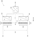
- FIG. 1A illustrates a functional block diagram of one embodiment of a power switching topology 100 in accordance with aspects described herein.
- the power switching topology 100 includes a first DC/DC converter 102, a second DC/DC converter 104, a DC/AC inverter 106, a first DC voltage source 108, a second DC voltage source 110, a positive DC input 112, a midpoint 114, a negative DC input 116, and an AC output 118.
- the power switching topology 100 can include more than two DC/DC converters.
- the power switching topology 100 can include more than two DC voltage sources.
- the DC/AC inverter 106 is coupled to the first and second DC/DC converters 102, 104 and configured to receive DC outputs from the first and second DC/DC converters 102, 104.
- the DC/AC inverter 106 converts the DC outputs received from the first and second DC/DC converters 102, 104 into a plurality of AC output signals and provides the plurality of output AC signals to the AC output 118.
- the AC output 118 can include a plurality of AC outputs.
- the first DC voltage source 108 is coupled between the positive DC input 112 and the midpoint 114 and the second DC voltage source 110 is coupled between the midpoint 114 and the negative DC input 116.
- the midpoint 114 is coupled to ground (i.e., zero volts).
- the DC/AC inverter 106 is also coupled to the midpoint 114.
- An input DC voltage VDC can be split across the first DC voltage source 108 and the second DC voltage source 110.
- the input DC voltage VDC may be split evenly between the first and second DC voltage sources 108, 110.
- the first and second DC/DC converters 102, 104 may be configured to support a portion of the input DC voltage VDC (e.g., 50%).
- the first DC/DC converter 102 is coupled to the first DC voltage source 108 and to receive a first DC voltage VD1 (e.g., a first portion of VDC) from the first DC voltage source 108.
- the second DC/DC converter 104 is coupled to the second DC voltage source 110 and to receive a second DC voltage VD2 (e.g., a second portion of VDC) from the second DC voltage source 110.
- the DC voltage sources 108, 110 each include one or more capacitors coupled in series.
- the first DC voltage source 108 can include a plurality of capacitors coupled in series between the positive DC input 112 and the midpoint 114
- the second DC voltage source 110 can include a plurality of capacitors coupled between negative DC input 116 and the midpoint 114.
- the first DC/DC converter 102 includes a first input and a second input coupled across the plurality of capacitors of the first DC voltage source 108 to receive the first DC voltage VD1.
- the second DC/DC converter 104 includes a first input and a second input coupled across the plurality of capacitors of the second DC voltage source 110 to receive the second DC voltage VD2.
- the first and second DC/DC converters 102, 104 may include additional inputs coupled to the first and second DC voltage sources 108, 110.
- the first DC/DC converter 102 can include one or more additional inputs coupled between the plurality of capacitors of the first DC voltage source 108 to receive additional DC voltages from the first DC voltage source 108; i.e., different portions of the first DC voltage VD1.
- the second DC/DC converter 104 can include one or more additional inputs coupled between the plurality of capacitors of the second DC voltage source 110 to receive additional DC voltages from the second DC voltage source 110; i.e., different portions of the second DC voltage VD2.
- other types and arrangements of DC voltage sources may be used.
- the power switching topology 100 can include additional circuitry to maintain a desired voltage distribution between the first DC voltage source 108 and the second DC voltage source 110.
- FIG. 1B illustrates a functional block diagram of a power switching topology 120.
- the power switching topology 120 is substantially similar to the power switching circuit 100 of FIG. 1A , except the power switching topology 120 includes a DC bus balancer 122.
- the DC bus balancer 122 can be coupled to the positive DC input 112, the midpoint 114, and the negative DC input 116, and include one or more DC/DC converters configured to regulate the first and second DC voltages VD1, VD2.
- the DC bus balancer 122 is operated to maintain an equal distribution of the input DC voltage VDC across each of the DC voltage sources 108, 110. In other examples, the DC bus balancer 122 is operated to maintain a different distribution of the input DC voltage VDC across the DC voltage sources 108, 110.
- the power switching topology 100 can include more than two DC voltage sources. In certain examples, additional DC voltage sources may be included to optimize the voltage distribution between the first and second DC voltage sources 108, 110.
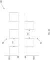
- FIG. 1C illustrates a functional block diagram of a power switching circuit 140 in accordance with aspects described herein.
- the power switching topology 140 is substantially similar to the power switching topology 100 of FIG. 1A , except the power switching circuit 150 includes a third DC voltage source 142.
- the third DC voltage source 142 is coupled between the first DC voltage source 108 and the second DC voltage source 110.
- the third DC voltage source 142 is configured to store an intermediate portion of the input DC voltage VDC.
- the first DC/DC converter 102 can be configured to receive a first upper portion (e.g., highest 30%) of the input DC voltage VDC and the second DC/DC converter 102 can be configured to receive a second lower portion (e.g., lowest 30%) of the input DC voltage VDC.
- the third DC voltage source 142 can be configured to store the intermediate portion (e.g., middle 40%) of the input DC voltage VDC.
- the power switching topology 140 includes additional circuitry to maintain a desired voltage distribution between the first, second, and third DC voltage sources 108, 110, 142.
- FIG. 1D illustrates a functional block diagram of a power switching topology 160 in accordance with aspects described herein.
- the power switching topology 160 is substantially similar to the power switching topology 140 of FIG. 1C , except the power switching topology 160 includes a DC bus balancer 162.
- the DC bus balancer is coupled across the first voltage source 108, the second voltage source 110, and the third voltage source 142 and includes one or more DC/DC converters configured to regulate the first and second DC voltages VD1, VD2, as well as the intermediate voltage across the third DC voltage source 142.
- the desired voltage distribution may be an unequal distribution across the DC voltage sources 108, 110, 142; however, in other examples, the desired distribution may be an equal distribution across the DC voltage sources 108, 110, 142.
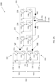
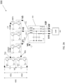
- FIG. 2A illustrates a schematic of a power switching circuit 200 in accordance with aspects described herein.
- the power switching circuit 200 corresponds to the power switching topology 100 of FIG. 1A ; however, in other examples, features corresponding to the power switching topologies 120, 140, and 160 of FIGS. 1B-1D can be included in the power switching circuit 200.
- the power switching circuit 200 includes a first DC/DC converter 202, a second DC/DC converter 204, a DC/AC inverter 206, a first DC voltage source 208, a second DC voltage source 210, a first DC input 212, a midpoint 214, and a second DC input 216.
- the first DC voltage source 208 is coupled between the first DC input 212 and the midpoint 214, and the first DC/DC converter 202 is coupled across the first DC voltage source 208.
- the first DC input 212 is a positive DC input.
- the second DC voltage source 210 is coupled between the second DC input 216 and the midpoint 214, and the second DC/DC converter 204 is coupled across the second DC voltage source 210.
- the second DC input 216 is a negative DC input.
- an input DC voltage VDC can be split across the first and second DC voltage sources 208, 210.
- the first DC voltage source 208 is configured to provide a first DC voltage VD1 and the second DC voltage source 210 is configured to provide a second DC voltage VD2.
- the first and second DC voltage sources 208, 210 can each include one or more capacitors coupled in series.
- a third DC voltage source and/or a bus balancer may be included as described above (e.g., power switching topologies 120, 140, 160).
- the DC/DC converters can each include m switching cells.
- a switching cell of the first DC/DC converter 202 includes a first switch 202a and a second switch 202b.
- the first switch 202a is coupled to a first side of the first DC voltage source 208 (e.g., the first DC input 212) and the second switch 202b is coupled to a second side of the first DC voltage source 208 (e.g., the midpoint 214).
- the first and second switches 202a, 202b can be arranged differently.
- the first and second switches 202a, 202b are configured to operate in a complementary manner.
- the first switch 202a when the first switch 202a is turned on (i.e., closed), the second switch 202b is turned off (i.e., opened), and vice versa.
- the first switch 202a is configured to receive a control signal cd 1 and the second switch 202b is configured to receive an inverted version of the control signal cd 1 .
- the first and second switches 202a, 202b can each receive independent control signals.
- a switching cell of the second DC/DC converter 204 includes a first switch 204a and a second switch 204b.
- the first switch 204a is coupled to a first side of the second DC voltage source 210 (e.g., the midpoint 214) and the second switch 204b is coupled to a second side of the second DC voltage source 210 (e.g., the second DC input 216).
- the first and second switches 204a, 204b can be arranged differently.
- the first and second switches 204a, 204b are configured to a complementary manner. As shown in FIG.
- the second switch 204b is configured to receive a control signal cd 2 and the first switch 204a is configured to receive an inverted version of the control signal cd 2 .
- the first and second switches 204a, 204b can each receive independent control signals.
- the first DC/DC converter 202 is operated to convert the first DC voltage VD1 provided by the first DC voltage source 208 into a variable DC voltage VP.
- the second DC/DC converter 204 is operated to convert the second DC voltage VD2 provided by the second DC voltage source 210 into a variable DC voltage VN.
- the first DC/DC converter 202 can provide the variable DC voltage VP to a first DC output 220 and the second DC/DC converter can provide the variable DC voltage VN to a second DC output 222.
- the DC/DC converters 202, 204 are only converting portions of the input DC voltage VDC (e.g., VD1, VD2) and not the full input DC voltage VDC, the DC/DC converters 202, 204 can operate at high switching frequencies with reduced switching losses.
- VDC input DC voltage
- VD1 full input DC voltage
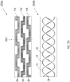
- FIG. 2B illustrates an example of the variable DC voltages VP and VN according to aspects described herein.
- the first DC/DC converter 202 is operated such that the variable DC voltage VP oscillates between the first DC voltage VD1 and the midpoint voltage V0
- the second DC/DC converter 204 is operated such that variable DC voltage VN oscillates between the midpoint voltage V0 and the second DC voltage VD2.
- VP has a first duty cycle 232
- VN has a second duty cycle 234.
- the duty cycles 232, 234 are substantially the same; however, in other examples the duty cycles 232, 234 may be different (e.g., adjusted by the controls signals cd 1 and cd 2 ) .
- the first and second DC/DC converters 202, 204 can be operated as DC choppers.
- the variable DC voltages VP and VN can each have substantially square (i.e., chopped) waveforms.
- the first and second DC outputs 220, 222 of the DC/DC converters 202, 204 can be coupled directly to the DC/AC inverter 206 (i.e., without filtering elements).
- each switching leg of the DC/AC inverter 206 includes k switching cells coupled between the first DC output 220 of the first DC/DC converter 202 and the second DC output 222 of the second DC/DC converter 204.
- a switching cell of the first switching leg 224 includes a first switch 224a and a second switch 224b coupled between the first DC output 220 and the second DC output 222.
- the first switch 224a is coupled between the first DC output 220 and a first AC output 218a
- the second switch 224b is coupled between the second DC output 222 and the first AC output 218a.
- a switching cell of the second switching leg 226 includes a first switch 226a coupled between the first DC output 220 and a second AC output 218b and a second switch 226b coupled between the second DC output 222 and the second AC output 218b.
- a switching cell of the third switching leg 228 includes a first switch 228a coupled between the first DC output 220 and a third AC output 218c and a second switch 228b coupled between the second DC output 222 and the third AC output 218c.
- the switching cell(s) of each switching leg may be arranged differently.
- the first and second switches of each switching cell are configured to operate in a complementary manner. For example, when the first switch is turned on (i.e., closed), the second switch is turned off (i.e., opened), and vice versa.
- each switching leg is operated in a first state by turning on the first switch and turning off the second switch such that the variable DC voltage VP is provided to the corresponding AC output (i.e., 218a, 218b, or 218c).
- each switching leg is operated in a second state by turning off the first switch and turning on the second switch such that the variable DC voltage VN is provided to the corresponding AC output (i.e., 218a, 218b, or 218c).
- each switching leg 224, 226, 228 can be controlled to operate in the first and second states via control signals.
- the switching cell of the first switching leg 224 is configured to receive a control signal ci 1 .
- the first switch 224a of the switching cell receives the control signal ci 1 and the second switch 224b of the switching cell receives an inverted version of the control signal ci 1 .
- the switching cells of the second and third switching legs 226, 228 are configured to receive corresponding control signals ci 2 and ci 3 in a similar manner.
- the first and second switches of the switching cells of each switching leg 224, 226, 228 can receive independent control signals.
- each switching leg 224, 226, 228 is operated in static and transition modes of operation to provide a plurality of output signals to the plurality of AC outputs 218.
- the static mode of each switching leg corresponds to the first and second states described above.
- the transition mode of each switching leg corresponds to a transition between the first and second states.
- each switching leg can provide either the variable DC voltage VP or the variable DC voltage VN to its corresponding AC output (i.e., 218a, 218b, or 218c).
- each switching leg is operated in the static mode to provide the most positive and negative portions of the plurality of output signals.
- each switching leg can provide at least a portion of the variable DC voltage VP and/or the variable DC voltage VN to its corresponding AC output (i.e., 218a, 218b, or 218c).
- each switching leg is operated in the transition mode to provide intermediate portions of the plurality of output signals.
- the switching legs can be controlled to cycle through the static and transition modes such that the synthesized plurality of output signals provided to the AC outputs 218a, 218b, 218c have phase offsets.
- the DC/AC inverter 206 can be configured to include a different number of switching legs and/or a different number of switching cells. Examples of such embodiments are described in greater detail below (e.g., FIG. 7A ).
- FIG. 2C is a graph illustrating control signal waveforms for operating the power switching circuit 200 in accordance with aspects described herein.
- the first DC/DC converter 202 is operated to convert the first DC voltage VD1 provided by the first DC voltage source 208 into the variable DC voltage VP and the second DC/DC converter 204 is operated to convert the second DC voltage VD2 provided by the second DC voltage source 210 into the variable DC voltage VN.
- the control signal cd 1 is oscillated to toggle the switches 202a, 202b of the switching cell of the first DC/DC converter 202 on and off to derive the variable DC voltage VP from the first DC voltage VD1.
- the control signal cd 2 is oscillated to toggle the switches 204a, 204b of the switching cell of the second DC/DC converter 204 on and off to derive the variable DC voltage VN from the second DC voltage VD2.
- the control signals cd 1 and cd 2 can be offset in time.
- the control signals cd 1 and cd 2 can be offset such that the first and second DC/DC converters 202, 204 are operated to provide offsetting variable DC voltages VP and VN (as shown in FIG. 2B ).
- the control signals cd 1 and cd 2 are pulse width modulation (PWM) signals.
- PWM pulse width modulation
- the control signals cd 1 and cd 2 may be arranged or aligned differently.
- the DC/AC inverter 206 is operated to provide the plurality of output signals to the plurality of AC outputs 218.
- the control signals ci 1 -ci 3 can be oscillated to cycle each of the switching legs 224, 226, 228 through the static and transition modes of operation to derive the plurality of output signals from the variable DC voltages VP and VN.
- the control signals ci 1 -ci 3 is high (e.g., 1)
- the corresponding switching leg is operated in the first state (i.e., static mode) to provide the variable DC voltage VP to its respective AC output (i.e., 218a, 218b, or 218c).
- the corresponding switching leg when each of the control signals ci 1 - ci 3 is low (e.g., 0), the corresponding switching leg is operated in the second state (i.e., static mode) to provide the variable DC voltage VN to its respective AC output. Likewise, when each of the control signals ci 1 - ci 3 is transitioning between high/low (i.e., transition mode), the corresponding switching leg provides at least a portion of the variable DC voltages VP and VN to its respective AC output.
- the DC/AC inverter 206 can be operated such that only one of the switching legs 224, 226, 228 is operated in the transition mode of operation and the remaining switching legs are operated in the static mode of operation at any given time.
- the first switching leg 224 is controlled by the control signal ci 1 to operate in the first state (i.e., static mode) to derive the most positive portion of its corresponding output signal from the variable DC voltage VP and the second switching leg 226 is controlled by the control signal ci 2 to operate in the second state (i.e., static mode) to derive the most negative portion of its corresponding output signal from the variable DC voltage VN.
- the third switching leg 228 is controlled by the control signal ci 3 to switch from the first state to the second state (i.e., transition mode).
- the third switching leg 228 derives an intermediate portion of its corresponding output signal from the variable DC voltages VP and VN.
- the first switching leg 224 is controlled by the control signal ci 1 to remain operating in the first state (i.e., static mode) and continue deriving the most positive portion of its corresponding output signal from the variable DC voltage VP.
- the third switching leg 228 is controlled by the control signal ci 3 to operate in the second state (i.e., static mode) to derive the most negative portion of its corresponding output signal from the variable DC voltage VN.
- the second switching leg 226 is controlled by the control signal ci 2 to switch from the second state to the first state (i.e., transition mode).
- the second switching leg 226 derives an intermediate portion of its corresponding output signal from the variable DC voltages VP and VN.
- the switching legs 224, 226, 228 can be continually cycled by the control signals ci 1 -ci 3 through the static and transition modes during time periods T3-T5 (and so on) to derive the plurality of output signals from the variable DC voltages VP and VN.
- switching losses can be reduced, improving the efficiency of the DC/AC inverter 206.
- the variable DC voltages VP and VN have chopped waveforms with zero voltage periods, switching losses in the DC/AC inverter 206 and the power switching circuit 200 can be reduced even further.
- VP has a peak amplitude that is substantially equal to the first DC voltage VD1 and VN has a peak amplitude that is substantially equal to the second DC voltage VD2.
- the DC/AC inverter 206 can be operated to minimize the amplitude of the differential voltage between the variable DC voltages VP and VN (e.g., by staggering the zero voltage periods). In some examples, by minimizing the amplitude of the differential voltage between the variable DC voltages VP and VN, stress on the DC/AC inverter 206 can be reduced while deriving the plurality of output signals.
- the control signals cd 1 and cd 2 can be oscillated at a frequency different than the frequency of the plurality of output signals.
- the control signals cd 1 and cd 2 are oscillated at a frequency faster than the plurality of output signals.
- the control signals ci 1 -ci 3 of the DC/AC inverter 206 are aligned relative to the control signals cd 1 and cd 2 of the DC/DC converters 202, 204 to provide desired phase offsets between the plurality of output signals.
- the control signals ci 1 -ci 3 can be staggered across cycles of the control signals cd 1 and cd 2 to generate the desired phase offsets between the plurality of output signals.
- control signals cd 1 and cd 2 can be offset/staggered such that switching legs operating in the transition mode can be coupled/decoupled between the first DC output 220 and the second DC output 222 during zero voltage periods of the variable DC voltages VP and VN (i.e., when VP and VN are providing V0).
- the third switching leg 228 is controlled by the control signal ci 3 to operate in the transition mode (first state to second state).
- the third switching leg 228 is decoupled from the first DC output 220 while the variable DC voltage VP is providing V0 (as indicated by cd 1 ) .
- the third switching leg 228 is coupled to the second DC output 222 while the variable DC voltage VN is providing V0 (as indicated by cd 2 ) .
- switching losses of the DC/AC inverter 206 can be reduced.
- the switching cell switches of each switching leg can be turned on/off while only a portion of the input DC voltage VDC is applied across each switching leg (i.e., VD1, VD2, or V0).
- VD1, VD2, or V0 the power handling requirements of the switching legs (and cells) can be reduced to improve the efficiency of the DC/AC inverter 206.
- switching components rated for lower power applications can be utilized to reduce cost.
- FIG. 2D illustrates a plurality of output signals of the power switching circuit 200 in accordance with aspects described herein.
- a first output voltage V1 corresponds to the output signal provided by the first switching leg 224 to the first AC output 218a
- a second output voltage V2 corresponds to the output signal provided by the second switching leg 226 to the second AC output 218b
- a third output voltage V3 corresponds to the output signal provided by the third switching leg 228 to the third AC output 218c.
- each of the AC voltages V1-V3 are derived from the variable DC voltages VP and VN, each can oscillate between VD1 and VD2.
- the first switching leg 224 is operated in the static mode (first state)
- the second switching leg 226 is operated in the static mode (second state)
- the third switching leg 228 is operated in the transition mode.
- the first switching leg 224 provides the most positive portion of the first output voltage V1
- the second switching leg 226 provides the most negative portion of the second output voltage V2
- the third switching leg 228 provides the intermediate portion of the third output voltage V3.
- the graph 260b illustrates an example of a first output current I1 associated with the first output voltage V1, a second output current I2 associated with the second output voltage V2, and a third output current I3 associated with the third output voltage V3.
- the plurality of output signals can be phase offset from one another.
- FIG. 3A illustrates a schematic of a power switching circuit 300 in accordance with aspects described herein.
- the power switching circuit 300 is substantially the same as the power switching circuit 200 of FIG. 2A , except the power switching circuit 300 includes a filter 302 coupled to the plurality of AC outputs 218a-218c to provide further conditioning of the plurality of output signals.
- the plurality of output signals V1-V3 may be subject to distortion resulting from operation (i.e., switching) of the DC/DC converters 202, 204 and the DC/AC inverter 206.
- the distortion corresponds to a third order harmonic of the switching frequency of the DC/DC converters 202, 204.
- the filter 302 is a lowpass filter configured to remove high frequency distortion injected by the DC/DC converters 202, 204 and the DC/AC inverter 206.
- the filter 302 is an LC filter; however, in other examples, different types of filters can be used and configured to remove different types of distortion.
- the filter 302 can provide a plurality of filtered output signals (e.g., V1f-V3f) to a load 304.
- the plurality of filtered output signals V1f-V3f can have a different waveform than the pre-filtered plurality of output signals.
- the plurality of output signals may have a first waveform (e.g., square wave) and the filter 302 can be configured to provide a plurality of filtered output signals having a second waveform (e.g., sinusoidal).
- FIG. 3B illustrates a graph 320 of the filtered output voltages in accordance with aspects described herein.
- the filtered output voltages V1f-V3f can oscillate between VD1 and VD2.
- the filtered output voltage 322 shown in the graph 320 corresponds to the first filtered output signal V1f when referenced to V0 (i.e., GND).
- the plurality of output signals can be phase offset from one another, and as such, can be referenced to one another to provide different variations of line output signals which oscillate above VD1 and below VD2.
- the first and second filtered output voltages V1f and V2f can be referenced to one another to provide the line output voltage 324 shown in FIG. 3B .
- the amount of phase offset between each output signal of the plurality of output signals depends on the specific power switching application (i.e., the load 304). For example, in three-phase power applications, where the load 304 is an electrical grid or motor, the power switching circuit 300 can generate the plurality of output signals with phase offsets in increments of 120° to provide a desired plurality of line output signals (e.g., line output voltage 324).
- the load 304 is an electrical grid or motor
- the power switching circuit 300 can generate the plurality of output signals with phase offsets in increments of 120° to provide a desired plurality of line output signals (e.g., line output voltage 324).
- DC/DC converters 202, 204 of the power switching circuit 200 are configured as two-level converters, in other examples, the DC/DC converters may be configured to provide more than two voltage levels.
- the DC/AC inverter 206 of the power switching circuit 200 is configured as a two-level inverter, in other examples, the DC/AC inverter 206 may be configured to operate with more than two voltage levels.
- the configurations of the DC/DC converters and the DC/AC inverter correspond to specific requirements of power switching applications. For example, in some power switching applications it may be desired to increase the output power capability of the DC/DC converters to support higher voltages.
- FIG. 4 illustrates a schematic of a power switching circuit 400 in accordance with aspects described herein. Similar to the power switching circuit 200 of FIG. 2A , the power switching circuit 400 includes a first DC/DC converter 402, a second DC/DC converter 404, and a DC/AC inverter 406.
- the DC/DC converters 402, 404 each include multiple switching cells (i.e., m switching cells). In certain examples, increasing the number of switching cells (i.e., m ) can improve the power handling capability of the DC/DC converters 402, 404.
- the number of switching cells included in each DC/DC converter may correspond to the amplitude of the DC input voltage(s). In some examples, the inclusion of additional switching cells can improve the voltage distribution across switching cells and may allow for the voltage ratings of individual switches to be reduced.
- the first DC/DC converter 402 includes a first switching cell 402a and a second switching cell 402b.
- the second DC/DC converter 404 includes a first switching cell 404a and a second switching cell 404b.
- one or more capacitors can be coupled between the switching cells of each DC/DC converter 402, 404 to store portions of the DC voltages provided to the DC/DC converters 402, 404.
- the number of capacitors included in each DC/DC converter 402, 404 corresponds to m-1.
- the first DC/DC converter 402 can include a first capacitor 403 coupled between the first and second switching cells 402a, 402b and the second DC/DC converter 404 can include a second capacitor 405 coupled between the first and second switching cells 404a, 404b.
- the first capacitor 403 is configured to store at least a portion of the first DC voltage VD1 provided to the first DC/DC converter 402 and the second capacitor 405 is configured to store at least a portion of the second DC voltage VD2 provided to the second DC/DC converter 404.
- the DC/DC converters 402, 404 can include more than two switching cells ( m >2), and capacitors can be coupled between second and third switching cells of each DC/DC converter in a similar manner, and so on.
- the portions of the DC voltages (VD1, VD2) stored by each capacitor correspond to the number of switching cells in each DC/DC converter 402, 404 (i.e., m ) and the amount of current drawn by each switching cell.
- the power switching circuit 400 can include DC voltage source selectors 408a and 408b to selectively provide various portions of the first and second DC voltages VD1, VD2 to the DC/DC converters 402, 404. (e.g., VD1/2, VD2/2, etc.).
- the DC/DC converters 402, 404 can be configured to provide more than two voltage levels.
- the variable DC voltages generated by the DC/DC converters 402, 404 can oscillate between more than two voltage levels (e.g., V0, VD1/2, VD1, VD2/2, VD2, etc.).
- the voltage selectors 408a, 408b can each include one or more switching cells that can be operated to provide the various DC voltages to the DC/DC converters 402, 404.
- the DC/AC inverter 406 is configured as three-phase Neutral Point Clamped (NPC) inverter.
- NPC Neutral Point Clamped
- the DC/AC inverter 406 is operated in a similar manner as to the DC/AC inverter 206 of the power switching circuit 200 of FIG. 2A .
- the DC/AC inverter 406 can operate with one switching leg in a transition mode and the remaining switching legs in a static mode to provide a plurality of output signals to the load 408.
- the NPC inverter configuration provides the ability to support the variable DC voltages VP and VN using series coupled switches with reduced voltage ratings.
- FIG. 5 illustrates a schematic of a power switching circuit 500 in accordance with aspects described herein. Similar to the power switching circuit 200 of FIG. 2A , the power switching circuit 500 includes a first DC/DC converter 502, a second DC/DC converter 504, and a DC/AC inverter 506.
- the DC/DC converters 502, 504 are configured as Flying Capacitor Multi-Level (FCML) converters.
- FCML Flying Capacitor Multi-Level
- the DC/DC converters 502, 504 can be operated as three-level converters.
- the FCMI, configuration provides the ability to operate the switches of the DC/DC converters 502, 504 at reduced switching frequencies, as the apparent switching frequency is doubled at the output of each DC/DC converter 502, 504.
- the DC/DC converters 502, 504 can be operated to provide reduced switching/conduction losses and lower harmonic distortion.
- the FCMI configuration is isolated from the supply voltage midpoint (i.e., V0)
- the inclusion of a DC bus balancer may be optional.
- the DC/AC inverter 506 can include a different number of switching legs, a different number of switching cells, and/or a different inverter topology.
- the power switching circuit 500 is operated in a similar manner as to the power switching circuit 200 of FIG. 2A .
- the DC/DC converters 502, 504 can be operated to generate variable DC voltages from various portions of the input DC voltage VDC and the DC/AC inverter 506 can be operated to provide a plurality of output signals to the load 508.
- FIG. 6A illustrates a schematic of a power switching circuit 600 in accordance with aspects described herein. Similar to the power switching circuit 200 of FIG. 2A , the power switching circuit 600 includes a first DC/DC converter 602, a second DC/DC converter 604, and a DC/AC inverter 606.
- T-NPC T-Type NPC
- the power switching circuit 600 can be operated in a similar manner as to the examples described above to provide a plurality of output signals.
- the T-NPC inverter configuration can be operated to provide the midpoint voltage (i.e., V0) to the inverter outputs (e.g., A, B, C) during transition states to reduce output voltage distortion.
- FIG. 6B illustrates a schematic of a power switching circuit 650 in accordance with aspects described herein.
- the power switching circuit 650 is substantially the same as the power switching circuit 600 of FIG. 6A , except the power switching circuit 650 includes additional switches 652a, 652b, 654a, and 654b.
- the additional switches 652a and 652b can be coupled in parallel with the first DC/DC converter 602 and controlled to reduce conduction losses associated with operation of the first DC/DC converter 602.
- the additional switches 654a and 654b can be coupled in parallel with the second DC/DC converter 604 and controlled to reduce conduction losses associated with operation of the second DC/DC converter 604.
- the additional switches may be transistors such as MOSFETs, IGBTs, BJTs; however, in other examples the additional switches may be diodes.
- the additional switches may be a transistor with a parallel-coupled diode.
- FIG. 7A illustrates a schematic of a power switching circuit 700 in accordance with aspects described herein. Similar to the power switching circuit 200 of FIG. 2A , the power switching circuit 700 includes a first DC/DC converter 702, a second DC/DC converter 704, and a DC/AC inverter 706.
- the DC/AC inverter 706 is configured as a three-phase NPC inverter (i.e., three-level).
- the DC/AC inverter 706 can be operated as a three-level inverter configured to receive DC input voltages from the first DC/DC converter 702, the second DC/DC converter 704, and a midpoint/neutral connection.
- the power switching circuit 700 can be operated in a similar manner as to the examples described above to provide a plurality of output signals with increased power handling capability.
- FIG. 7B illustrates a schematic of a power switching circuit 750 in accordance with aspects described herein.
- the power switching circuit 750 is substantially the same as the power switching circuit 700, except the power switching circuit 750 includes additional switches 724a, 724b, 726a, 726b, 728a, and 728b.
- the additional switches 724a and 724b are coupled in parallel with a first switching leg 724 of the DC/AC inverter 706 and controlled to reduce conduction losses associated with operation of the DC/AC inverter 706.
- the additional switches 726a and 726b are coupled in parallel with a second switching leg 726 of the DC/AC inverter 706 and the additional switches 728a and 728b are coupled in parallel with a third switching leg 728 of the DC/AC inverter 706 and controlled to reduce conduction losses associated with the operation of the DC/AC inverter 706.
- the additional switches can improve current sharing within the DC/AC inverter 706.
- the additional switches each have the same voltage/current ratings as the other inverter switches, and as such, the voltage and current applied to each switch of the DC/AC inverter 706 can be reduced.
- the additional switches may be configured with different semiconductor technologies (e.g., Silicon, Silicon Carbide, Gallium Nitride, etc.) to optimize current sharing.
- the additional switches may be transistors such as MOSFETs, IGBTs, or BJTs; however, in other examples the additional switches may be diodes.
- the additional switches may be a transistor with a parallel-coupled diode.
- additional switches may be coupled in series with the first and/or second switches of switching cells included in the DC/DC converters 702, 704 and/or the DC/AC inverter 706.
- the additional switches can be configured as different device types and/or with different semiconductor technologies to further reduce losses.
- a pair of switches may be configured as a hybrid Silicon IGBT - Silicon Carbide MOSFET device. During operation, the Silicon Carbide MOSFET can be switched prior to the Silicon IGBT, allowing the Silicon IGBT to switch at a lower voltage (e.g., 0V). As such, switching losses associated with the Silicon IGBT can be reduced or eliminated.
- different types of devices and/or semiconductor technologies may be utilized depending on the power switching application.
- FIG. 8A illustrates a block diagram of a power drive system 800 in accordance with aspects described herein.
- the power drive system 800 includes an active front end (i.e., rectifier) 804, a first DC chopper stage 806, a DC bus balancer 808, a first DC voltage source 810, a second DC voltage source 812, a third DC voltage source 814, a second DC chopper stage 816, and a DC/AC inverter 818.
- the active front end 804 is configured to receive AC power from an electrical grid 802, convert the received AC power into DC power having an input DC voltage VDC, and provide the input DC voltage VDC to the first DC chopper stage 806.
- a first DC/DC converter 806a of the first DC chopper stage 806 receives a first DC voltage VD1 (i.e., a first portion of VDC) and a second DC/DC converter 806b of the first DC chopper stage 806 receives a second DC voltage VD2 (i.e., a second portion of VDC).
- the first and second DC/DC converters 806a, 806b can be operated in a similar manner as the DC/DC converters described in the examples above (e.g., the DC/DC converters 202, 204 of the power switching circuit 200 of FIG. 2A ).
- the first DC/DC converter 806a generates a variable DC voltage VP1 from the first DC voltage VD1 and provides the variable DC voltage VP1 to the first DC voltage source 810.
- the second DC/DC converter 806b generates a variable DC voltage VN1 from the second DC voltage VD2 and provides the variable DC voltage VN1 to the second DC voltage source 812.
- the third DC voltage source 814 is coupled between the first and second DC voltage sources 810, 812 to support intermediate portions of the variable DC voltages VP1 and VN1.
- the bus balancer 808 is configured to regulate the distribution of the variable DC voltages VP1 and VN1 across the DC voltage sources 810, 812, 814.
- the first DC voltage source 810 provides at least a portion of the variable DC voltage VP1 to a first DC/DC converter 816a of the second chopper stage 816.
- the second DC voltage source 812 provides at least a portion of the variable DC voltage VN1 to a second DC/DC converter 816b of the second chopper stage 816.
- the first and second DC/DC converters 816a, 816b can be operated in a similar manner as the DC/DC converters 806a, 806b of the first chopper stage 806.
- the first DC/DC converter 816a generates a variable DC voltage VP2 from at least a portion of the variable DC voltage VP1 and the second DC/DC converter 816b generates a variable DC voltage VN2 from at least a portion of the variable DC voltage VN1.
- the variable DC voltages VP2 and VN2 may oscillate between different (e.g., lower) voltage levels than the variable DC voltages VP1 and VN1.
- the variable DC voltages VP2 and VN2 are provided to the DC/AC inverter 818.
- the DC/AC inverter 818 can be operated in a similar manner as the DC/AC inverters described in the examples above (e.g., the DC/AC inverter 206 of the power switching circuit 200 of FIG. 2A ). As such, the DC/AC inverter 818 can be operated to provide a plurality of output signals to the load 820.
- FIG. 8B illustrates a schematic diagram of the power drive system 800 in accordance with aspects described herein.
- the DC voltages sources 810, 812, and 814 can include a plurality of capacitors.
- An example of a multi-level bus balancer 808 coupled to each of the DC voltage sources 810, 812, and 814 is shown.
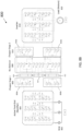
- FIG. 9A illustrates a block diagram of an uninterruptible power supply (UPS) system 900 in accordance with aspects described herein.
- the UPS system 900 includes an active front end 904, a DC/AC inverter 906, a first DC/DC converter 908, a second DC/DC converter 910, a DC bus 912, a first DC voltage source 914, a second DC voltage source 916, a third voltage source 918, and a DC bus balancer 920.
- the active front end 904, the DC/AC inverter 906, and the first and second DC/DC converters 908, 910 are each be coupled to the DC bus 912.
- the DC bus 912 includes a positive rail 912a coupled to the active front end 904, the DC/AC inverter 906, and the first DC/DC converter 908 and a negative rail 912b coupled to the active front end 904, the DC/AC inverter 906, and the second DC/DC converter 910.
- the active front end 904 is an AC/DC converter (e.g., rectifier) configured to receive AC power from an electrical grid 902 and convert the received AC power into DC power having an input DC voltage VDC.
- the input DC voltage VDC is provided to the first DC voltage source 914 and the second DC voltage source 916 via the first and second DC/DC converters 908, 910.
- the third DC voltage source 918 is coupled between the first and second DC voltage sources 914, 916 to store an intermediate portion of the input DC voltage VDC.
- the bus balancer 918 is configured to regulate the distribution of the input DC voltage VDC across the DC voltage sources 914, 916, 918.
- the first and second DC/DC converters 908, 910 can be operated in a similar manner as the DC/DC converters described above (e.g., the DC/DC converters 202, 204 of the power switching circuit 200 of FIG. 2A ).
- the first DC/DC converter 908 generates a variable DC voltage VP from a first portion VD1 of the input DC voltage VDC.
- the second DC/DC converter 910 generates a variable DC voltage VN from a second portion VD2 of the input DC voltage VDC.
- the variable DC voltages VP and VN are provided to the DC/AC inverter 906 via the positive and negative DC bus rails 912a, 912b.
- the DC/AC inverter 906 is configured to operate in a similar manner as the DC/AC inverters described above (e.g., the DC/AC inverter 206 of the power switching circuit 200 of FIG. 2A ).
- the DC/AC inverter 206 can include a plurality of switching legs configured to be operated in the static and transition states to derive a plurality of output signals from the variable DC voltages VP and VN.
- the plurality of output signals may be AC signals provided to the load 920.
- the active front end 904 is configured to operate as a bi-directional converter. For example, in addition to converting AC power received from the grid 902, the active front end 904 can receive DC power from the DC bus 912 (i.e., the variable DC voltages VP and VN), convert the DC power to AC power, and backfeed AC power to the grid 902.
- DC bus 912 i.e., the variable DC voltages VP and VN
- FIG. 9B illustrates a schematic diagram of the UPS system 900 in accordance with aspects described herein.
- the DC voltages sources 914 and 916 can include a plurality of capacitors.
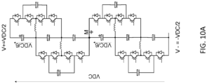
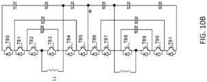
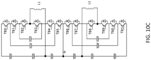
- FIGS. 10A-10D illustrate various DC bus balancer configurations in accordance with aspects described herein.
- Each of the DC bus balancer configurations of FIGS. 10A-10D can be included in any of the power switching circuits and systems described above.
- each of the DC bus balancer configurations can be utilized as the DC bus balancers 122, 162 of the power switching topologies 120, 160 of FIGS. 1B and 1D .
- each DC bus balancer configuration can be utilized as the DC bus balancer 808 of the power driver system 800 of FIG. 8A and the DC bus balancer 920 of the UPS system 900 of FIG. 9A .
- FIG. 11 is a graph illustrating choke current ripple as a function of duty cycle for various DC bus balancer configurations in accordance with aspects described herein.
- the choke current ripple corresponds to the type of DC/DC converter being implemented in each DC bus balancer configuration and the operating duty cycle.
- trace 1102 in FIG. 11 corresponds to the choke current ripple of a DC bus balancer configuration implemented as a 3-level DC/DC converter.
- the choke current ripple can be minimized by operating the 3-level DC/DC converter with a 50% duty cycle.
- trace 1104 corresponds to the choke current ripple of a DC bus balancer configuration implemented as a 4-level DC/DC converter, and the choke ripple can be minimized by operating the 4-level DC/DC converter with a 33% or 66% duty cycle.
- current ripple and choke volume can be minimized.
- a controller may be configured to operate any of the power switching circuits and systems described above.
- the controller can control any of the DC/DC converters, DC/AC inverters, or other circuitry provided herein. Using data stored in associated memory, the controller may be operable to execute one or more instructions that may result in the manipulation of one or more power switches included in the power conversion circuitry.
- the controller can include one or more processors or other types of controllers. The controller may perform a portion of the functions discussed herein on a processor, and perform another portion using an Application-Specific Integrated Circuit (ASIC) tailored to perform particular operations. Examples in accordance with the present invention may perform the operations described herein using many specific combinations of hardware and software and the invention is not limited to any particular combination of hardware and software components.
- ASIC Application-Specific Integrated Circuit
- a first conversion stage generates variable DC voltages from input DC voltages and a second conversion stage derives a plurality of AC output signals from the variable DC voltages.
- the variable DC voltages are provided using multi-level DC/DC converters and the AC outputs are derived using a DC/AC inverter.
- Such topologies can provide improved efficiency in medium- and high-voltage power switching applications, and in some examples, efficiency and power density can be improved along with reductions in cost.
Landscapes
- Engineering & Computer Science (AREA)
- Power Engineering (AREA)
- Business, Economics & Management (AREA)
- Emergency Management (AREA)
- Inverter Devices (AREA)
- Dc-Dc Converters (AREA)
Claims (14)
- Eine Schaltung zum Leistungsschalten, die Folgendes beinhaltet:einen ersten DC(Gleichstrom)-Bus und einen zweiten DC-Bus;einen ersten DC-DC-Wandler (102, 202, 402, 502, 602, 702, 802, 902, 908), der Folgendes aufweist: einen ersten Eingang, der mit dem ersten DC-Bus gekoppelt ist und konfiguriert ist, um eine erste DC-Eingangsspannung, die einem ersten zugewiesenen Teil einer DC-Eingangsspannung zwischen dem ersten DC-Bus und dem zweiten DC-Bus entspricht, zu empfangen, und einen Ausgang, der konfiguriert ist, um eine erste DC-Ausgangsspannung bereitzustellen;einen zweiten DC-DC-Wandler (104, 204, 404, 504, 604, 704, 804, 904, 910), der Folgendes aufweist: einen ersten Eingang, der mit dem zweiten DC-Bus gekoppelt ist und konfiguriert ist, um eine zweite DC-Eingangsspannung, die einem zweiten zugewiesenen Teil der DC-Eingangsspannung zwischen dem ersten DC-Bus und dem zweiten DC-Bus entspricht, zu empfangen, und einen Ausgang, der konfiguriert ist, um eine zweite DC-Ausgangsspannung bereitzustellen;eine erste DC-Spannungsquelle (108, 208) und eine zweite DC-Spannungsquelle (110, 210), die zwischen dem ersten DC-Bus und dem zweiten DC-Bus gekoppelt sind, wobei die erste DC-Spannungsquelle konfiguriert ist, um dem ersten DC-DC-Wandler die erste DC-Eingangsspannung bereitzustellen, und die zweite DC-Spannungsquelle konfiguriert ist, um dem zweiten DC-DC-Wandler die zweite DC-Eingangsspannung bereitzustellen, wobei der erste und der zweite OC-OC-Wandler jeweils m Schaltzellen, m ≥ 1, umfassen und jede Schaltzelle der m Schaltzellen mindestens einen ersten Schalter und einen zweiten Schalter umfasst, wobei der erste und der zweite Schalter konfiguriert sind, um in komplementären Zuständen betrieben zu werden;einen DC-AC(Wechselstrom)-Wechselrichter, der einen ersten Eingang, der mit dem Ausgang des ersten DC-DC-Wandlers gekoppelt ist, und einen zweiten Eingang, der mit dem Ausgang des zweiten DC-DC-Wandlers gekoppelt ist, aufweist, wobei der DC-AC-Wechselrichter n Schaltarme umfasst, wobei jeder Schaltarm k Schaltzellen aufweist, die zwischen dem ersten Eingang und dem zweiten Eingang gekoppelt sind, wobei n > 2 und k > 1; undmindestens eine Steuereinheit, die mit dem ersten DC-DC-Wandler, dem zweiten DC-DC-Wandler und dem DC-AC-Wechselrichter gekoppelt ist, dadurch gekennzeichnet, dass die mindestens eine Steuereinheit konfiguriert ist, um den DC-AC-Wechselrichter so zu betreiben, dass dieser mindestens einer Last, die mit dem DC-AC-Wechselrichter gekoppelt ist, n AC-Signale bereitstellt, indem zu jeder Zeit zwei der n Schaltarme in einem statischen Zustand und die verbleibenden n-2 der n Schaltarme in einem Übergangszustand betrieben werden, wobei sich die Begriffe statischer Zustand und Übergangszustand auf den Zustand der Steuersignale zum Ansteuern der Schalter in einem Arm beziehen, und wobei die Schaltung zum Leistungsschalten konfiguriert ist, um eine Oszillationsfrequenz eines Steuersignals (cd1) für den ersten DC-DC-Wandler und eine Oszillationsfrequenz eines Steuersignals (cd2) für den zweiten DC-DC-Wandler zu erzielen, die höher sind als eine Oszillationsfrequenz der n AC-Ausgangssignale, und die Steuersignale (ci1, ci2, ci3) des DC-AC-Wechselrichters relativ zu den Steuersignalen (cd1, cd2) der DC-DC-Wandler ausgerichtet sind.
- Schaltung zum Leistungsschalten gemäß Anspruch 1, wobei der erste DC-Bus ein positiver DC-Bus ist und der zweite DC-Bus ein negativer DC-Bus ist.
- Schaltung zum Leistungsschalten gemäß Anspruch 1, wobei die Steuereinheit ferner konfiguriert ist, um den ersten DC-DC-Wandler so zu betreiben, dass die erste DC-Ausgangsspannung eine positive variable DC-Spannung ist, die einen ersten Tastgrad aufweist, und den zweiten DC-DC-Wandler so zu betreiben, dass die zweite DC-Ausgangsspannung eine negative variable DC-Spannung ist, die einen zweiten Tastgrad aufweist.
- Schaltung zum Leistungsschalten gemäß Anspruch 3, wobei der erste Eingang des DC-AC-Wechselrichters direkt mit dem Ausgang des ersten DC-DC-Wandlers gekoppelt ist, um die positive variable DC-Spannung zu empfangen, und der zweite Eingang des DC-AC-Wechselrichters direkt mit dem Ausgang des zweiten DC-DC-Wandlers gekoppelt ist, um die negative variable DC-Spannung zu empfangen.
- Schaltung zum Leistungsschalten gemäß Anspruch 4, wobei jeder Schaltarm, der in dem statischen Zustand betrieben wird, konfiguriert ist, um der Last eine statische Ausgangsspannung bereitzustellen, die von einer von der positiven variablen DC-Spannung und der negativen variablen DC-Spannung abgeleitet ist, wobei die statische Ausgangsspannung einem von dem positivsten und dem negativsten Teil der n AC-Signale entspricht.
- Schaltung zum Leistungsschalten gemäß Anspruch 5, wobei ein Ausgang jedes Schaltarms, der in dem statischen Zustand betrieben wird, über mindestens eine der k Schaltzellen mit einem von dem ersten und dem zweiten Eingang des DC-AC-Wechselrichters gekoppelt ist.
- Schaltung zum Leistungsschalten gemäß Anspruch 4, wobei jeder Schaltarm, der in dem Übergangszustand betrieben wird, konfiguriert ist, um der mindestens einen Last eine Übergangsausgangsspannung bereitzustellen, die von der positiven variablen DC-Spannung und der negativen variablen DC-Spannung abgeleitet ist, wobei die Übergangsausgangsspannung Zwischenteilen der n AC-Signale entspricht.
- Schaltung zum Leistungsschalten gemäß Anspruch 7, wobei ein Ausgang jedes Schaltarms, der in dem Übergangszustand betrieben wird, über mindestens eine der k Schaltzellen zwischen mindestens dem ersten und dem zweiten Eingang des DC-AC-Wechselrichters geschaltet wird.
- Schaltung zum Leistungsschalten gemäß Anspruch 1, wobei die Schaltung zum Leistungsschalten als eine unterbrechungsfreie Stromversorgung (USV) konfiguriert ist und ferner Folgendes beinhaltet:einen Eingang, der konfiguriert ist, um mit einer AC-Quelle gekoppelt zu sein und AC-Eingangsleistung von der AC-Quelle zu empfangen;einen Wandler, der mit dem Eingang gekoppelt ist und konfiguriert ist, um die AC-Eingangsleistung in DC-Leistung umzuwandeln und dem ersten und dem zweiten DC-Bus DC-Leistung bereitzustellen.
- Ein Verfahren zum Betreiben einer Schaltung zum Leistungsschalten, das Folgendes beinhaltet:Bereitstellen, durch eine erste DC-Spannungsquelle (108, 208) für einen ersten DC-DC-Wandler (102, 202, 402, 502, 602, 702, 802, 902, 908), einer ersten DC-Eingangsspannung;Bereitstellen, durch eine zweite DC-Spannungsquelle (110, 120) für einen zweiten DC-DC-Wandler (104, 204, 404, 504, 604, 704, 804, 904, 910), einer zweiten DC-Eingangsspannung;Empfangen der ersten DC-Eingangsspannung an einem Eingang des ersten DC-DC-Wandlers, der mit einem ersten DC-Bus gekoppelt ist, und der zweiten DC-Eingangsspannung an einem Eingang des zweiten DC-DC-Wandlers, der mit einem zweiten DC-Bus gekoppelt ist, wobei die erste DC-Eingangsspannung einem ersten zugewiesenen Teil einer DC-Eingangsspannung zwischen dem ersten DC-Bus und dem zweiten DC-Bus entspricht und die zweite DC-Eingangsspannung einem zweiten zugewiesenen Teil der DC-Eingangsspannung zwischen dem ersten DC-Bus und dem zweiten DC-Bus entspricht, wobei der erste und der zweite OC-OC-Wandler jeweils m Schaltzellen, m ≥ 1, umfassen und jede Schaltzelle der m Schaltzellen mindestens einen ersten Schalter und einen zweiten Schalter umfasst, wobei der erste und der zweite Schalter konfiguriert sind, um in komplementären Zuständen betrieben zu werden;Steuern des ersten DC-DC-Wandlers, um eine erste DC-Spannung bereitzustellen, und des zweiten DC-DC-Wandlers, um eine zweite DC-Spannung bereitzustellen;Empfangen der ersten DC-Spannung an einem ersten Eingang eines DC-AC-Wechselrichters und Empfangen der zweiten DC-Spannung an einem zweiten Eingang des DC-AC-Wechselrichters, wobei der DC-AC-Wechselrichter n Schaltarme aufweist, die k Schaltzellen aufweisen, wobei k > 1 und n > 2; undSteuern des DC-AC-Wechselrichters, um n AC-Ausgangssignale bereitzustellen, die von der ersten und der zweiten DC-Spannung abgeleitet sind, indem zu jeder Zeit zwei der n Schaltarme in einem statischen Zustand und die verbleibenden n-2 Schaltarme in einem Übergangszustand betrieben werden, wobei sich die Begriffe statischer Zustand und Übergangszustand auf den Zustand der Steuersignale zum Ansteuern der Schalter in einem Arm beziehen, und wobei die Schaltung zum Leistungsschalten konfiguriert ist, um eine Oszillationsfrequenz eines Steuersignals (cd1) für den ersten DC-DC-Wandler und eine Oszillationsfrequenz eines Steuersignals (cd2) für den zweiten DC-DC-Wandler zu erzielen, die höher sind als eine Oszillationsfrequenz der n AC-Ausgangssignale, und die Steuersignale (ci1, ci2, ci3) des DC-AC-Wechselrichters relativ zu den Steuersignalen (cd1, cd2) der DC-DC-Wandler ausgerichtet sind.
- Verfahren gemäß Anspruch 10, wobei das Steuern des ersten DC-DC-Wandlers, um die erste DC-Spannung bereitzustellen, ferner das Betreiben des ersten DC-DC-Wandlers derart umfasst, dass die erste DC-Spannung eine erste variable DC-Spannung ist, die einen ersten Tastgrad aufweist, und das Steuern des zweiten DC-DC-Wandlers, um die zweite DC-Spannung bereitzustellen, ferner das Betreiben des zweiten DC-DC-Wandlers derart umfasst, dass die zweite DC-Spannung eine zweite variable DC-Spannung ist, die einen zweiten Tastgrad aufweist.
- Verfahren gemäß Anspruch 11, wobei das Betreiben jedes jeweiligen Schaltarms in dem statischen Zustand das Steuern des Schaltarms umfasst, um eine statische Ausgangsspannung bereitzustellen, die von einer von der ersten variablen DC-Spannung und der zweiten variablen DC-Spannung abgeleitet ist, wobei die statische Ausgangsspannung einem von dem positivsten und dem negativsten Teil der n AC-Ausgangssignale entspricht.
- Verfahren gemäß Anspruch 11, wobei das Betreiben jedes jeweiligen Schaltarms in dem Übergangszustand das Steuern des Schaltarms umfasst, um eine Ausgangsspannung bereitzustellen, die von der ersten variablen DC-Spannung und der zweiten variablen DC-Spannung abgeleitet ist, wobei die Übergangsausgangsspannung Zwischenteilen der n AC-Ausgangssignale entspricht.
- Ein Computerprogramm, das Computerprogrammcodes beinhaltet und die Verfahrensschritte gemäß einem der Ansprüche 10-13 durchführt, wenn es auf einem Datenverarbeitungssystem ausgeführt wird, das konfiguriert ist, um mit einer Schaltung zum Leistungsschalten gemäß Anspruch 1 kompatibel zu sein.
Applications Claiming Priority (1)
| Application Number | Priority Date | Filing Date | Title |
|---|---|---|---|
| US201962858239P | 2019-06-06 | 2019-06-06 |
Publications (3)
| Publication Number | Publication Date |
|---|---|
| EP3748838A1 EP3748838A1 (de) | 2020-12-09 |
| EP3748838C0 EP3748838C0 (de) | 2024-08-21 |
| EP3748838B1 true EP3748838B1 (de) | 2024-08-21 |
Family
ID=70968807
Family Applications (1)
| Application Number | Title | Priority Date | Filing Date |
|---|---|---|---|
| EP20177526.9A Active EP3748838B1 (de) | 2019-06-06 | 2020-05-29 | Mehrstufige wechselrichtertopologien für mittel- und hochspannungsanwendungen |
Country Status (3)
| Country | Link |
|---|---|
| US (1) | US11581821B2 (de) |
| EP (1) | EP3748838B1 (de) |
| CN (1) | CN112054704B (de) |
Families Citing this family (7)
| Publication number | Priority date | Publication date | Assignee | Title |
|---|---|---|---|---|
| EP3675345A1 (de) * | 2018-12-31 | 2020-07-01 | Solaredge Technologies Ltd. | Ausgleichskondensatorleistungswandler |
| GB2611697A (en) * | 2020-07-22 | 2023-04-12 | Hitachi High Tech Corp | DC high-voltage source device and charged particle beam device |
| CN113114061B (zh) * | 2021-03-26 | 2022-06-24 | 台达电子企业管理(上海)有限公司 | 变换器及抑制变换器的环流干扰的方法 |
| CN113328649A (zh) * | 2021-05-18 | 2021-08-31 | 华为技术有限公司 | 一种变换电路及其控制方法 |
| US11777414B2 (en) * | 2021-07-02 | 2023-10-03 | Schneider Electric It Corporation | Interleaved power conversion systems and methods |
| US11670945B1 (en) | 2022-02-28 | 2023-06-06 | Lunar Energy, Inc. | Power optimizers in series with voltage sensors and a common reference signal |
| JP7812492B1 (ja) | 2024-10-22 | 2026-02-09 | 株式会社Tmeic | 無停電電源装置 |
Citations (2)
| Publication number | Priority date | Publication date | Assignee | Title |
|---|---|---|---|---|
| CN104682753A (zh) * | 2015-01-28 | 2015-06-03 | 浙江大学 | 零电压开关三相三电平二极管中点箝位逆变器及其调制方法 |
| US20170310238A1 (en) * | 2016-04-22 | 2017-10-26 | Futurewei Technologies, Inc. | Apparatus and method for an active-switched inverter |
Family Cites Families (18)
| Publication number | Priority date | Publication date | Assignee | Title |
|---|---|---|---|---|
| US6570780B2 (en) * | 2001-05-17 | 2003-05-27 | Honda Giken Kogyo Kabushiki Kaisha | Resonant inverter control system |
| JP2008517582A (ja) * | 2004-10-20 | 2008-05-22 | シーメンス ヴィディーオー オートモーティヴ コーポレイション | 電力システム、方法および装置 |
| US7974106B2 (en) * | 2007-05-07 | 2011-07-05 | Bloom Energy Corporation | Ripple cancellation |
| US8100799B2 (en) * | 2007-09-12 | 2012-01-24 | GM Global Technology Operations LLC | Method and system for controlling power inverters in electric drives of vehicles with two-mode transmissions |
| US8288891B2 (en) * | 2008-05-02 | 2012-10-16 | Bloom Energy Corporation | Integrated fuel cell system with auxiliary power delivery |
| KR101113508B1 (ko) * | 2010-05-06 | 2012-02-29 | 성균관대학교산학협력단 | 태양광 pcs 일체형 양방향 배터리 충방전 시스템 및 방법 |
| CN102832880B (zh) | 2011-06-17 | 2017-03-01 | 迪尔阿扣基金两合公司 | 控制转换器的方法 |
| US9602025B2 (en) * | 2013-07-12 | 2017-03-21 | Infineon Technologies Austria Ag | Multiphase power converter circuit and method |
| JP6454936B2 (ja) | 2014-05-12 | 2019-01-23 | パナソニックIpマネジメント株式会社 | 電力変換装置、およびそれを用いたパワーコンディショナ |
| EP2988408A1 (de) * | 2014-08-21 | 2016-02-24 | ABB Technology Oy | Schaltabzweigung für dreistufigen Umrichter und Verfahren zur Steuerung einer Schaltabzweigung des dreistufigen Umrichters |
| DE102015210920A1 (de) * | 2015-06-15 | 2016-12-15 | TRUMPF Hüttinger GmbH + Co. KG | Redox-Flow-Batteriesystem und Verfahren zum Erkennen eines Fehlers in einer Brückenschaltung eines DC/DC-Wandlers eines Redox-Flow-Batteriesystems |
| US10547191B2 (en) * | 2016-06-15 | 2020-01-28 | Schneider Electric It Corporation | Power management unit for intelligent traffic system applications |
| DE102017215133A1 (de) | 2016-08-31 | 2018-03-01 | Siemens Aktiengesellschaft | Inverter und Photovoltaikanlage |
| US20180083525A1 (en) * | 2016-09-22 | 2018-03-22 | Ahmed Fayez Abu-Hajar | Method for generating harmonics free dc to ac inverters |
| US10461575B2 (en) * | 2017-03-28 | 2019-10-29 | Schneider Electric It Corporation | Multistate PWM command for 3 levels inverters |
| CN108736757B (zh) * | 2018-06-01 | 2021-02-09 | 东南大学 | 一种电流源型无电解电容高频链变换器系统 |
| CN110707953B (zh) * | 2018-07-10 | 2025-02-18 | 施耐德电气It公司 | 准五电平逆变器 |
| FR3084798B1 (fr) | 2018-08-03 | 2020-10-30 | Schneider Electric Ind Sas | Convertisseur de puissance multiniveaux |
-
2020
- 2020-05-26 US US16/883,174 patent/US11581821B2/en active Active
- 2020-05-29 EP EP20177526.9A patent/EP3748838B1/de active Active
- 2020-06-05 CN CN202010506134.6A patent/CN112054704B/zh active Active
Patent Citations (2)
| Publication number | Priority date | Publication date | Assignee | Title |
|---|---|---|---|---|
| CN104682753A (zh) * | 2015-01-28 | 2015-06-03 | 浙江大学 | 零电压开关三相三电平二极管中点箝位逆变器及其调制方法 |
| US20170310238A1 (en) * | 2016-04-22 | 2017-10-26 | Futurewei Technologies, Inc. | Apparatus and method for an active-switched inverter |
Also Published As
| Publication number | Publication date |
|---|---|
| EP3748838A1 (de) | 2020-12-09 |
| US20200389099A1 (en) | 2020-12-10 |
| EP3748838C0 (de) | 2024-08-21 |
| CN112054704A (zh) | 2020-12-08 |
| CN112054704B (zh) | 2024-06-18 |
| US11581821B2 (en) | 2023-02-14 |
Similar Documents
| Publication | Publication Date | Title |
|---|---|---|
| EP3748838B1 (de) | Mehrstufige wechselrichtertopologien für mittel- und hochspannungsanwendungen | |
| US6838925B1 (en) | Three level inverter | |
| US10063162B2 (en) | Multi level inverter | |
| US11095232B2 (en) | Hybrid I-T type multi-level converters | |
| CA2578585A1 (en) | Nine device ac-to-ac converter | |
| WO2015109094A1 (en) | Split phase power conversion apparatuses, methods and systems | |
| EP4396934B1 (de) | Fliegender kondensatorwandler mit spannungsausgleichsschaltung | |
| Majdoul et al. | A nine-switch nine-level voltage inverter new topology with optimal modulation technique | |
| Wang et al. | A new control strategy for modular multilevel converter operating in quasi two-level PWM mode | |
| KR101484105B1 (ko) | 단일 입력 전압원을 갖는 멀티레벨 인버터 | |
| Jafari et al. | New mmc-based multilevel converter with two-and-one set of arms and one inductor | |
| Wang et al. | Step-up switched-capacitor multilevel inverter employing multiple inputs with reduced switches | |
| Shahir et al. | 16-level basic topology for cascaded multilevel inverters with reduced number of components | |
| Li et al. | A hybrid Si/GaN-based quasi-single-stage converter for microgrid applications with simplified space-vector modulation | |
| Pribadi et al. | A six-level T-type ANPC inverter for medium-voltage applications | |
| KR100928549B1 (ko) | 스위치 클램프트 멀티-레벨 인버터 | |
| KR101718303B1 (ko) | 단일 입력 전압원과 배터리 직병렬 결합을 이용한 멀티레벨 인버터 | |
| Goel et al. | Higher Level Multilevel Inverter for Medium Voltage Drives with High DC-link Voltage Utilization | |
| Yamarthi et al. | ” neutral point clamped and cascaded H-bridge multilevel inverter topologies–a comparison | |
| Dong et al. | A sic & si hybrid four-level anpc converter with multi-step soft-switching modulation achieving capacitor voltage balancing | |
| Foti et al. | A simple DC-link voltage balancing strategy for NPC three-level inverters | |
| Picas et al. | Discontinuous modulation of modular multilevel converters without the need for extra submodules | |
| Surasmi et al. | Power Quality Improvement in Multilevel Inverters using Open-end Winding Motor Scheme | |
| Sun et al. | Research on topology and PWM control method of a novel cascaded multilevel inverter | |
| Roy et al. | Opal-rt based analysis and implementation of single phase cascaded multilevel inverter with minimum number of switches |
Legal Events
| Date | Code | Title | Description |
|---|---|---|---|
| PUAI | Public reference made under article 153(3) epc to a published international application that has entered the european phase |
Free format text: ORIGINAL CODE: 0009012 |
|
| STAA | Information on the status of an ep patent application or granted ep patent |
Free format text: STATUS: THE APPLICATION HAS BEEN PUBLISHED |
|
| AK | Designated contracting states |
Kind code of ref document: A1 Designated state(s): AL AT BE BG CH CY CZ DE DK EE ES FI FR GB GR HR HU IE IS IT LI LT LU LV MC MK MT NL NO PL PT RO RS SE SI SK SM TR |
|
| AX | Request for extension of the european patent |
Extension state: BA ME |
|
| STAA | Information on the status of an ep patent application or granted ep patent |
Free format text: STATUS: REQUEST FOR EXAMINATION WAS MADE |
|
| STAA | Information on the status of an ep patent application or granted ep patent |
Free format text: STATUS: EXAMINATION IS IN PROGRESS |
|
| 17P | Request for examination filed |
Effective date: 20210608 |
|
| RBV | Designated contracting states (corrected) |
Designated state(s): AL AT BE BG CH CY CZ DE DK EE ES FI FR GB GR HR HU IE IS IT LI LT LU LV MC MK MT NL NO PL PT RO RS SE SI SK SM TR |
|
| 17Q | First examination report despatched |
Effective date: 20210702 |
|
| RIC1 | Information provided on ipc code assigned before grant |
Ipc: H02M 1/00 20060101ALN20240206BHEP Ipc: H02M 7/49 20070101ALN20240206BHEP Ipc: H02M 7/483 20070101ALI20240206BHEP Ipc: H02M 7/487 20070101AFI20240206BHEP |
|
| GRAP | Despatch of communication of intention to grant a patent |
Free format text: ORIGINAL CODE: EPIDOSNIGR1 |
|
| STAA | Information on the status of an ep patent application or granted ep patent |
Free format text: STATUS: GRANT OF PATENT IS INTENDED |
|
| RIC1 | Information provided on ipc code assigned before grant |
Ipc: H02M 1/00 20060101ALN20240223BHEP Ipc: H02M 7/49 20070101ALN20240223BHEP Ipc: H02M 7/483 20070101ALI20240223BHEP Ipc: H02M 7/487 20070101AFI20240223BHEP |
|
| INTG | Intention to grant announced |
Effective date: 20240322 |
|
| GRAS | Grant fee paid |
Free format text: ORIGINAL CODE: EPIDOSNIGR3 |
|
| GRAA | (expected) grant |
Free format text: ORIGINAL CODE: 0009210 |
|
| STAA | Information on the status of an ep patent application or granted ep patent |
Free format text: STATUS: THE PATENT HAS BEEN GRANTED |
|
| AK | Designated contracting states |
Kind code of ref document: B1 Designated state(s): AL AT BE BG CH CY CZ DE DK EE ES FI FR GB GR HR HU IE IS IT LI LT LU LV MC MK MT NL NO PL PT RO RS SE SI SK SM TR |
|
| RAP3 | Party data changed (applicant data changed or rights of an application transferred) |
Owner name: SCHNEIDER ELECTRIC IT CORPORATION |
|
| REG | Reference to a national code |
Ref country code: GB Ref legal event code: FG4D |
|
| REG | Reference to a national code |
Ref country code: CH Ref legal event code: EP |
|
| REG | Reference to a national code |
Ref country code: IE Ref legal event code: FG4D |
|
| REG | Reference to a national code |
Ref country code: DE Ref legal event code: R096 Ref document number: 602020036057 Country of ref document: DE |
|
| U01 | Request for unitary effect filed |
Effective date: 20240918 |
|
| U07 | Unitary effect registered |
Designated state(s): AT BE BG DE DK EE FI FR IT LT LU LV MT NL PT RO SE SI Effective date: 20241008 |
|
| PG25 | Lapsed in a contracting state [announced via postgrant information from national office to epo] |
Ref country code: NO Free format text: LAPSE BECAUSE OF FAILURE TO SUBMIT A TRANSLATION OF THE DESCRIPTION OR TO PAY THE FEE WITHIN THE PRESCRIBED TIME-LIMIT Effective date: 20241121 |
|
| PG25 | Lapsed in a contracting state [announced via postgrant information from national office to epo] |
Ref country code: GR Free format text: LAPSE BECAUSE OF FAILURE TO SUBMIT A TRANSLATION OF THE DESCRIPTION OR TO PAY THE FEE WITHIN THE PRESCRIBED TIME-LIMIT Effective date: 20241122 Ref country code: PL Free format text: LAPSE BECAUSE OF FAILURE TO SUBMIT A TRANSLATION OF THE DESCRIPTION OR TO PAY THE FEE WITHIN THE PRESCRIBED TIME-LIMIT Effective date: 20240821 |
|
| PG25 | Lapsed in a contracting state [announced via postgrant information from national office to epo] |
Ref country code: IS Free format text: LAPSE BECAUSE OF FAILURE TO SUBMIT A TRANSLATION OF THE DESCRIPTION OR TO PAY THE FEE WITHIN THE PRESCRIBED TIME-LIMIT Effective date: 20241221 |
|
| PG25 | Lapsed in a contracting state [announced via postgrant information from national office to epo] |
Ref country code: HR Free format text: LAPSE BECAUSE OF FAILURE TO SUBMIT A TRANSLATION OF THE DESCRIPTION OR TO PAY THE FEE WITHIN THE PRESCRIBED TIME-LIMIT Effective date: 20240821 |
|
| PG25 | Lapsed in a contracting state [announced via postgrant information from national office to epo] |
Ref country code: ES Free format text: LAPSE BECAUSE OF FAILURE TO SUBMIT A TRANSLATION OF THE DESCRIPTION OR TO PAY THE FEE WITHIN THE PRESCRIBED TIME-LIMIT Effective date: 20240821 Ref country code: RS Free format text: LAPSE BECAUSE OF FAILURE TO SUBMIT A TRANSLATION OF THE DESCRIPTION OR TO PAY THE FEE WITHIN THE PRESCRIBED TIME-LIMIT Effective date: 20241121 |
|
| PG25 | Lapsed in a contracting state [announced via postgrant information from national office to epo] |
Ref country code: RS Free format text: LAPSE BECAUSE OF FAILURE TO SUBMIT A TRANSLATION OF THE DESCRIPTION OR TO PAY THE FEE WITHIN THE PRESCRIBED TIME-LIMIT Effective date: 20241121 Ref country code: PL Free format text: LAPSE BECAUSE OF FAILURE TO SUBMIT A TRANSLATION OF THE DESCRIPTION OR TO PAY THE FEE WITHIN THE PRESCRIBED TIME-LIMIT Effective date: 20240821 Ref country code: NO Free format text: LAPSE BECAUSE OF FAILURE TO SUBMIT A TRANSLATION OF THE DESCRIPTION OR TO PAY THE FEE WITHIN THE PRESCRIBED TIME-LIMIT Effective date: 20241121 Ref country code: IS Free format text: LAPSE BECAUSE OF FAILURE TO SUBMIT A TRANSLATION OF THE DESCRIPTION OR TO PAY THE FEE WITHIN THE PRESCRIBED TIME-LIMIT Effective date: 20241221 Ref country code: HR Free format text: LAPSE BECAUSE OF FAILURE TO SUBMIT A TRANSLATION OF THE DESCRIPTION OR TO PAY THE FEE WITHIN THE PRESCRIBED TIME-LIMIT Effective date: 20240821 Ref country code: GR Free format text: LAPSE BECAUSE OF FAILURE TO SUBMIT A TRANSLATION OF THE DESCRIPTION OR TO PAY THE FEE WITHIN THE PRESCRIBED TIME-LIMIT Effective date: 20241122 Ref country code: ES Free format text: LAPSE BECAUSE OF FAILURE TO SUBMIT A TRANSLATION OF THE DESCRIPTION OR TO PAY THE FEE WITHIN THE PRESCRIBED TIME-LIMIT Effective date: 20240821 |
|
| PG25 | Lapsed in a contracting state [announced via postgrant information from national office to epo] |
Ref country code: SM Free format text: LAPSE BECAUSE OF FAILURE TO SUBMIT A TRANSLATION OF THE DESCRIPTION OR TO PAY THE FEE WITHIN THE PRESCRIBED TIME-LIMIT Effective date: 20240821 |
|
| PG25 | Lapsed in a contracting state [announced via postgrant information from national office to epo] |
Ref country code: CZ Free format text: LAPSE BECAUSE OF FAILURE TO SUBMIT A TRANSLATION OF THE DESCRIPTION OR TO PAY THE FEE WITHIN THE PRESCRIBED TIME-LIMIT Effective date: 20240821 |
|
| PG25 | Lapsed in a contracting state [announced via postgrant information from national office to epo] |
Ref country code: SK Free format text: LAPSE BECAUSE OF FAILURE TO SUBMIT A TRANSLATION OF THE DESCRIPTION OR TO PAY THE FEE WITHIN THE PRESCRIBED TIME-LIMIT Effective date: 20240821 |
|
| PLBE | No opposition filed within time limit |
Free format text: ORIGINAL CODE: 0009261 |
|
| STAA | Information on the status of an ep patent application or granted ep patent |
Free format text: STATUS: NO OPPOSITION FILED WITHIN TIME LIMIT |
|
| U20 | Renewal fee for the european patent with unitary effect paid |
Year of fee payment: 6 Effective date: 20250526 |
|
| PGFP | Annual fee paid to national office [announced via postgrant information from national office to epo] |
Ref country code: GB Payment date: 20250526 Year of fee payment: 6 |
|
| 26N | No opposition filed |
Effective date: 20250522 |
|
| REG | Reference to a national code |
Ref country code: CH Ref legal event code: H13 Free format text: ST27 STATUS EVENT CODE: U-0-0-H10-H13 (AS PROVIDED BY THE NATIONAL OFFICE) Effective date: 20251223 |
|
| PG25 | Lapsed in a contracting state [announced via postgrant information from national office to epo] |
Ref country code: CH Free format text: LAPSE BECAUSE OF NON-PAYMENT OF DUE FEES Effective date: 20250531 |
|
| PG25 | Lapsed in a contracting state [announced via postgrant information from national office to epo] |
Ref country code: MC Free format text: LAPSE BECAUSE OF FAILURE TO SUBMIT A TRANSLATION OF THE DESCRIPTION OR TO PAY THE FEE WITHIN THE PRESCRIBED TIME-LIMIT Effective date: 20240821 |