EP3748698A1 - Halbleiterkörper, lawinenphotodiode und verfahren zur herstellung eines halbleiterkörpers - Google Patents
Halbleiterkörper, lawinenphotodiode und verfahren zur herstellung eines halbleiterkörpers Download PDFInfo
- Publication number
- EP3748698A1 EP3748698A1 EP19188664.7A EP19188664A EP3748698A1 EP 3748698 A1 EP3748698 A1 EP 3748698A1 EP 19188664 A EP19188664 A EP 19188664A EP 3748698 A1 EP3748698 A1 EP 3748698A1
- Authority
- EP
- European Patent Office
- Prior art keywords
- region
- semiconductor body
- sinker
- buried layer
- conductivity
- Prior art date
- Legal status (The legal status is an assumption and is not a legal conclusion. Google has not performed a legal analysis and makes no representation as to the accuracy of the status listed.)
- Pending
Links
Images


Classifications
-
- H—ELECTRICITY
- H10—SEMICONDUCTOR DEVICES; ELECTRIC SOLID-STATE DEVICES NOT OTHERWISE PROVIDED FOR
- H10F—INORGANIC SEMICONDUCTOR DEVICES SENSITIVE TO INFRARED RADIATION, LIGHT, ELECTROMAGNETIC RADIATION OF SHORTER WAVELENGTH OR CORPUSCULAR RADIATION
- H10F30/00—Individual radiation-sensitive semiconductor devices in which radiation controls the flow of current through the devices, e.g. photodetectors
- H10F30/20—Individual radiation-sensitive semiconductor devices in which radiation controls the flow of current through the devices, e.g. photodetectors the devices having potential barriers, e.g. phototransistors
- H10F30/21—Individual radiation-sensitive semiconductor devices in which radiation controls the flow of current through the devices, e.g. photodetectors the devices having potential barriers, e.g. phototransistors the devices being sensitive to infrared, visible or ultraviolet radiation
- H10F30/22—Individual radiation-sensitive semiconductor devices in which radiation controls the flow of current through the devices, e.g. photodetectors the devices having potential barriers, e.g. phototransistors the devices being sensitive to infrared, visible or ultraviolet radiation the devices having only one potential barrier, e.g. photodiodes
- H10F30/225—Individual radiation-sensitive semiconductor devices in which radiation controls the flow of current through the devices, e.g. photodetectors the devices having potential barriers, e.g. phototransistors the devices being sensitive to infrared, visible or ultraviolet radiation the devices having only one potential barrier, e.g. photodiodes the potential barrier working in avalanche mode, e.g. avalanche photodiodes
-
- H—ELECTRICITY
- H10—SEMICONDUCTOR DEVICES; ELECTRIC SOLID-STATE DEVICES NOT OTHERWISE PROVIDED FOR
- H10F—INORGANIC SEMICONDUCTOR DEVICES SENSITIVE TO INFRARED RADIATION, LIGHT, ELECTROMAGNETIC RADIATION OF SHORTER WAVELENGTH OR CORPUSCULAR RADIATION
- H10F39/00—Integrated devices, or assemblies of multiple devices, comprising at least one element covered by group H10F30/00, e.g. radiation detectors comprising photodiode arrays
- H10F39/10—Integrated devices
- H10F39/107—Integrated devices having multiple elements covered by H10F30/00 in a repetitive configuration, e.g. radiation detectors comprising photodiode arrays
-
- H—ELECTRICITY
- H10—SEMICONDUCTOR DEVICES; ELECTRIC SOLID-STATE DEVICES NOT OTHERWISE PROVIDED FOR
- H10F—INORGANIC SEMICONDUCTOR DEVICES SENSITIVE TO INFRARED RADIATION, LIGHT, ELECTROMAGNETIC RADIATION OF SHORTER WAVELENGTH OR CORPUSCULAR RADIATION
- H10F71/00—Manufacture or treatment of devices covered by this subclass
- H10F71/121—The active layers comprising only Group IV materials
Definitions
- the semiconductor body comprises a first region of a first type of conductivity and a shallow region of a second type of conductivity that is arranged at the first region.
- a voltage is provided to the shallow region and the first region such that a space-charge region is generated between the first region and the shallow region.
- the first type of conductivity may be n-type (the regions and layers of the first type of conductivity are n-doped).
- the second type of conductivity may be p-type (the regions and layers of the second type of conductivity are p-doped).
- the word “encircles” means surrounds or encompasses in a plane of the semiconductor body such as e.g. at the first surface or another plane of the semiconductor body that is parallel to the first surface.
- the separating region encircles at least one of the sinker and the buried layer in planes of the semiconductor body that are different from the first surface, especially below the first surface.
- a doping concentration of the separating region is lower than a doping concentration of the sinker and/or the buried layer.
- this gradient results in an electric field that hinders electrons to reach an avalanche multiplication region.
- the semiconductor body comprises an isolation region located at the first surface of the semiconductor body.
- the isolation region encircles the sinker at the first surface.
- the isolation region may be realized as a shallow trench isolation.
- the isolation region separates one avalanche photodiode from an adjacent avalanche photodiode.
- the sinker encircles the first region.
- the first region and the enhancement region are enclosed by the sinker, the buried layer and the shallow region at each border or nearly each border.
- the first region and the enhancement region are enclosed by crystal material.
- disturbances and a not desired generation of charge carries is avoided at the border of the buried layer and the shallow region.
- a doping concentration of the sinker is higher than the minimum doping concentration of the first region.
- the sinker extends from the first surface of the semiconductor body to the buried layer.
- the buried layer is electrically connected via the sinker by a low-resistance connection.
- the sinker has a first doping concentration at the first surface of the semiconductor body. This region may be realized by a sinker contact region of the sinker.
- the sinker has a second doping concentration in a region between the first surface of the semiconductor body and the buried layer. The second doping concentration is lower than the first doping concentration and lower than a maximum doping concentration of the buried layer. The second doping concentration may be higher than the minimum doping concentration of the first region.
- the separating region encircles the sinker.
- the semiconductor body comprises a deep trench.
- the deep trench includes at least one isolating layer.
- the deep trench provides a good isolation between adjacent avalanche photodiodes.
- the deep trench encircles the separating region.
- the separating region is located between the sinker and the deep trench.
- the separating region encircles the buried layer.
- the buried layer may be named buried region.
- the separating region is located between the sinker and the buried layer.
- the semiconductor body comprises a guard ring of the second type of conductivity located at the first surface of the semiconductor body and encircling the shallow region.
- a doping concentration of the guard ring is lower than a doping concentration of the shallow region.
- the semiconductor body comprises a shield ring of the first type of conductivity.
- the shield ring is arranged between the guard ring and the buried layer.
- a doping concentration of the shield ring is lower than the doping concentration of the buried layer and may be higher than a minimum doping concentration of the first region.
- the shield ring may be fabricated by the WPE.
- the semiconductor body comprise a substrate.
- the substrate may be at a second surface of the semiconductor body.
- the buried layer is arranged between the substrate and the first region.
- the substrate may have the first type of conductivity.
- a doping concentration of the substrate is lower than the doping concentration of the buried layer.
- the doping concentration of the first region may be equal or approximately equal to the doping concentration of the substrate at least at some areas of the first region.
- the doping concentration of the separating region may be equal or approximately equal to the doping concentration of the substrate at least at some areas of the separating region.
- an avalanche photodiode comprises the semiconductor body and a stack of at least one isolating layer and at least one metallization layer.
- the stack is located at the first surface of the semiconductor body.
- the avalanche photodiode may be implemented as single-photon avalanche photodiode, abbreviated SPAD.
- SPAD single-photon avalanche photodiode
- the avalanche photodiode may be back side illuminated (in this case, the light goes through the buried layer to the first region) or front side illuminated (in this case, the light goes through the stack to the shallow region).
- a time-of-flight arrangement may comprise the avalanche photodiode.
- a low jitter is advantageous in this application.
- An avalanche photodiode such as a SPAD or an array of avalanche photodiodes such as SPADs may be applied e.g. for time of flight measurement, a four quadrant SPAD detector for adaptive optics, quantum key distribution, single molecule spectroscopy, single molecule conformational dynamics, DNA analysis by capillary electrophoresis, DNA fragment separation in a microchip, a matrix detector for analysis of protein microarray, fluorescence correlation spectroscopy, fluorescence lifetime spectroscopy and/or fluorescence lifetime imaging.
- a method for fabricating a semiconductor body comprises
- a separating region of the first type of conductivity encircles at least one of the sinker and the buried layer.
- a first region has a first type of conductivity and is between the buried layer and the shallow region.
- the separating region reduces the timing jitter.
- the sinker is fabricated at least partially using a well proximity effect during fabrication of the buried layer.
- the lower part of the sinker and the buried layer are fabricated at the same time, e.g. using one mask and one ion implantation step or using one mask and two ion implantation steps or using one mask and more than one ion implantation step.
- the lower part of the sinker and the buried layer are fabricated by two high energy implantation steps with e.g. 2000 keV and 1500 keV implantation energy.
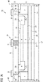
- the semiconductor body 11 comprises a sinker 35.
- the sinker 35 is at the first surface 13 of the semiconductor body 11.
- the sinker 35 may be realized as a well, e.g. as a p well.
- the sinker 35 may have a sinker contact region 36 at the first surface 13 of the semiconductor body 11.
- the sinker 35 is of the first type of conductivity.
- the sinker contact region 36 is a highly doped region of the first type of conductivity.
- the sinker 35 may extend up to the buried layer 25.
- a second part 20 of the metallization layer 15 may be coupled by a contact 21 to the sinker 35 and more especially to the sinker contact region 36.
- the second part 20 of the metallization layer 15 is electrically connected by the contact 21 and the sinker 35 to the buried layer 25.
- the first region 26 has a part between the guard ring 29 and the buried layer 25.
- the first region 26 has a further part between the guard ring 29 and the sinker 35.
- the deep trench 39 is manufactured from the front side.
- the deep trench 39 is fabricated from the first surface 13.
- a device may comprise an array of avalanche photodiodes 10, wherein each of the avalanche photodiodes 10 is realized as the example elucidated in Figure 1A .
- the device may comprise an array of pixels, wherein each pixel comprises one avalanche photodiode 10.
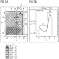
- the avalanche photodiode 10 as shown in Figure 1A has an extension DP in the cross-section.
- the extension DP may be called "device pitch”.
- the cross-section of the avalanche photodiode 10 is shown between a first border 48 which may be called "right border” and a second border 49 which may be called "left border”.
- the results achieved with a first avalanche photodiode are marked with AA and the results achieved with a second avalanche photodiode are marked with BB.
- the counts decrease up to a level which corresponds to the dark count rate, abbreviated as DCR.
- the width of the shown distribution of the counts is called a jitter.
- the jitter is typically specified as Full-width-at-half-maximum (abbreviated FWHM) or the full width at 10% of the maximum.
- FWHM Full-width-at-half-maximum
- the jitter is lower for the measurements marked with BB in comparison to the measurements marked with AA.
- the measurements marked with AA also result in a higher DCR in comparison to the measurements marked with BB.
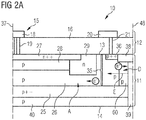
- FIG 2A shows an example of a cross-section of an avalanche photodiode 10.
- the semiconductor body 11 comprises a separating region 60.
- the separating region 60 encircles the sinker 35.
- the separating region 60 encompasses or surrounds the sinker 35.
- the isolation region 38 encircles the sinker 35.
- the separating region 60 and the isolation region 38 together encircle the sinker 35.
- the separating region 60 encircles the sinker 35 in depths between the isolation region 38 and the buried layer 25.
- the separating region 60 is located between the deep trench 39 and the sinker 35.
- the deep trench 39 is separated from the sinker 35 by the separating region 60.
- the buried layer 25 extends from the deep trench 39 at the first border 48 of the avalanche diode 10 to the second border 49 of the avalanche diode 10.
- the deep trench 39 is realized by an isolating material.
- This interface may cause the generation of electrons.
- the electrons are driven to the deep trench 39 and do not reach the avalanche multiplication region 50.
- the avalanche photodiode 10 comprises a spacing between the sinker 35 (named p-well) and the deep trench 39 realized by the separating region 60.
- the avalanche photodiode 10 includes a split guard ring.
- the sinker 35 is shared between two neighboring cells or pixels (i.e. one implant mask opening).
- the split guard ring there are two separate openings in the mask.
- the split guard ring is formed e.g. by the sinker 35 of one pixel, the separating region 60 of this pixel, a separating region of the neighboring pixel and the sinker of the neighboring pixel.
- the two separating regions are one structure on the mask.
- the portion of the DCR that originates from the deep trench 39 is reduced.
- the sinker 35 is realized using the well proximity effect, abbreviated WPE.
- the buried layer 25 is fabricated using a mask that is realized such that a photoresist covers an area near the first and the second border 48, 49.
- the photoresist may cover the area of the isolation region 38.
- This mask has the effect that a buried layer 25 is realized wherein the buried layer 25 has a gap (which is formed by the separating region 60) to the deep trench 39.
- the separation region 60 between the sinker 35 and the deep trench 39 as well as between the buried layer 25 and the deep trench 39 is a result of this photoresist.
- the photoresist has the effect that ions are scattered from the photoresist into the semiconductor body 11 such that the doping concentration of the first type of conductivity is increased in the area between the first surface 13 and the buried layer 25 such that the sinker 35 is fabricated.
- the sinker 35 is fabricated by doping atoms during implantation of the buried layer 25 using the WPE effect.
- the semiconductor body 11 comprises a shield ring 62 that is arranged between the guard ring 29 and the buried layer 25.
- the shield ring 62 is of the first type of conductivity.
- the shield ring 62 encircles the first region 26.
- the doping of the shield ring 62 is fabricated using the WPE effect.
- a doping concentration of the shield ring 62 is lower than a maximum doping concentration of the buried layer 25.
- the doping concentration of the shield ring 62 may be also lower than a maximum doping concentration of the enhancement region 28.
- the doping concentration of the shield ring 62 is higher than the doping concentration of the substrate 40.
- the doping concentration of the shield ring 62 may be similar to the doping concentration of the separating region 60, as shown in Figure 3D .
- arrow I indicates an area with a negative electric field along most of the deep trench 39.
- arrow J indicates an area with a negative electric field all along the deep trench 39.
- arrow K indicates an area with a negative electric field. No carriers generated right from here can reach the avalanche multiplication region 50.
- Figures 5A and 5B show details of characteristics of the avalanche photodiode 10 fabricated using WPE, as shown in Figures 2B and 3C .
- FIG 5A details of the doping concentration of the sinker 35 are shown.
- the sinker 35 realized using WPE (for example as shown in Figures 2B , 3C and 5A ) differs from the sinker 35 as shown in Figures 1A , 1B , 2A , 3A and 3B .
- a doping concentration of the sinker 35 as shown in Figures 1A , 1B , 2A typically has a high value from the first surface 13 of the semiconductor body 11 up to the buried layer 25.
- the doping concentration inside the sinker 35 may be approximately constant from the first surface 13 to the buried layer 35. Contrary to that, as shown in Figures 5A and 3C , the minimum of the doping concentration of the sinker 35 is lower than the maximum of the doping concentration of the buried layer 25 and also of sinker contact region 36.
- some regions of the sinker 35 are not directly below the sinker contact region 38.
- the doping concentration of the sinker 35 created by the WPE, has certain properties related to the WPE:
- the doping concentration of the sinker 35 is always lower than the highest doping concentration of the buried layer 25.
- the highest doping concentration of the buried layer 25 is five times larger than the doping concentration of the sinker 35 (typically the ratio is 10 times to 20 times).
- the width of the sinker 35 is larger closer to the first surface 13 (this is indicated by the two arrows L and M).
- the sinker 35 may have a wasp waist shape.
- the sinker 35 has a decreasing lateral dimension with increasing distance from the first surface 13.
- the following figures 6A to 11D show examples of layouts of masks for the fabrication of the avalanche diode 10.
- the example layouts mostly show octagonal structures.
- the layouts may also be quadratic, circular or rectangular.
- the layers and regions of the avalanche diode 10 in a top view are identical or approximately identical with the layout of the masks for fabricating these layers and regions. Differences may result e.g. from a diffusion process, overexposure or underexposure of photoresist etc.. In case of the buried layer 25 and the sinker 35, differences may result from the WPE, the large distance from the photoresist to the buried layer 25, a diffusion process and a high ion implantation dose and energy.
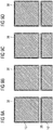
- Figures 6A , 7A , 8A , 9A , 10A and 11A show a top view of layouts of masks corresponding to the avalanche photodiode 10 shown in Figures 1A and 1B .
- Figures 6B , 7B , 8B , 9B , 10B and 11B show a top view corresponding to the example shown in Figure 2A .
- Figures 6C , 7C , 8C , 9C , 10C and 11C show top views corresponding to the example shown in Figure 2B .
- figures 6D , 7D , 8D , 9D , 10D and 11D show top views corresponding to the example shown in Figure 2D .
- the four avalanche photodiode 10 and the four further avalanche photodiode 10' shown in Figures 6A to 6D are typically not realized on one wafer or one die; instead the avalanche photodiode 10 and the further avalanche photodiode 10' shown in Figure 6A may be realized on one die, the avalanche photodiode 10 and the further avalanche photodiode 10' shown in Figure 6B may be realized on another die etc. The same applies to the other figures 7A to 11D .
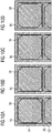
- Figures 7A to 7D show the layout of the masks that are already elucidated in Figures 6A to 6D and additionally the layout for the enhancement region 28 and the guard ring 29.
- the area of the enhancement region 28 is smaller in comparison to the area of the shallow region 27.
- the layout of the mask for the buried layer 25 shown in Figure 8C is designed such that the separating region 60 between the sinker 35 and the buried layer 25 on one side and the deep trench 35 on the other side can be realized.
- the mask for the buried layer 25 is realized such that a large gap between the buried layer 25 and the deep trench 39 is realized.
- the use of masks as shown in Figures 8C and 8D result into the WPE.
- Figures 11A to 11D show the examples of the layouts of different masks shown above with the exception of the masks of the isolation region 38 and the sinker contact region 36.
- inventions shown in Figures 1A to 11D as stated represent example embodiments of the improved semiconductor body, avalanche photodiode and method for fabricating a semiconductor body, therefore they do not constitute a complete list of all embodiments according to the improved semiconductor body, avalanche photodiode and method for fabricating.
- Actual semiconductor bodies, avalanche photodiodes and methods for fabricating may vary from the embodiments shown in terms of layers, shape, size and materials, for example.
Landscapes
- Light Receiving Elements (AREA)
Priority Applications (4)
| Application Number | Priority Date | Filing Date | Title |
|---|---|---|---|
| PCT/EP2020/065058 WO2020245061A1 (en) | 2019-06-03 | 2020-05-29 | Avalanche photodiode and method for fabricating an avalanche photodiode |
| US17/615,719 US12132132B2 (en) | 2019-06-03 | 2020-05-29 | Semiconductor body, avalanche photodiode and method for fabricating a semiconductor body |
| CN202080054968.6A CN114207846B (zh) | 2019-06-03 | 2020-05-29 | 雪崩光电二极管和用于制造雪崩光电二极管的方法 |
| TW109118460A TWI881979B (zh) | 2019-06-03 | 2020-06-02 | 半導體本體、累崩式光二極體以及半導體本體之製造方法 |
Applications Claiming Priority (1)
| Application Number | Priority Date | Filing Date | Title |
|---|---|---|---|
| EP19177926 | 2019-06-03 |
Publications (1)
| Publication Number | Publication Date |
|---|---|
| EP3748698A1 true EP3748698A1 (de) | 2020-12-09 |
Family
ID=66690270
Family Applications (1)
| Application Number | Title | Priority Date | Filing Date |
|---|---|---|---|
| EP19188664.7A Pending EP3748698A1 (de) | 2019-06-03 | 2019-07-26 | Halbleiterkörper, lawinenphotodiode und verfahren zur herstellung eines halbleiterkörpers |
Country Status (5)
| Country | Link |
|---|---|
| US (1) | US12132132B2 (de) |
| EP (1) | EP3748698A1 (de) |
| CN (1) | CN114207846B (de) |
| TW (1) | TWI881979B (de) |
| WO (1) | WO2020245061A1 (de) |
Cited By (3)
| Publication number | Priority date | Publication date | Assignee | Title |
|---|---|---|---|---|
| IT202100009443A1 (it) * | 2021-04-14 | 2022-10-14 | Fond Bruno Kessler | Un sensore di radiazioni |
| WO2023227365A1 (en) * | 2022-05-27 | 2023-11-30 | Ams-Osram Ag | Single photon avalanche diode and sensor array |
| EP4307396A1 (de) * | 2022-07-11 | 2024-01-17 | STMicroelectronics (Research & Development) Limited | Einzelphotonen-lawinendiode |
Families Citing this family (4)
| Publication number | Priority date | Publication date | Assignee | Title |
|---|---|---|---|---|
| DE102019204701A1 (de) * | 2019-04-02 | 2020-10-08 | MAX-PLANCK-Gesellschaft zur Förderung der Wissenschaften e.V. | Avalanche-Photodioden-Array |
| CN113299787B (zh) * | 2021-05-21 | 2022-04-29 | 武汉新芯集成电路制造有限公司 | 半导体器件及其制造方法 |
| EP4593090A4 (de) * | 2022-09-28 | 2026-01-14 | Trupixel Inc | Einzelphotonen-lawinendiode, elektronische vorrichtung und lidar-vorrichtung |
| CN115621352B (zh) * | 2022-10-31 | 2025-02-11 | 武汉新芯集成电路股份有限公司 | 半导体器件及其制造方法 |
Citations (3)
| Publication number | Priority date | Publication date | Assignee | Title |
|---|---|---|---|---|
| JP2008235510A (ja) * | 2007-03-20 | 2008-10-02 | Matsushita Electric Ind Co Ltd | 光半導体装置 |
| US20110272561A1 (en) * | 2010-03-23 | 2011-11-10 | Stmicroelectronics S.R.L. | Method of detecting impinging position of photons on a geiger-mode avalanche photodiode, related geiger-mode avalanche photodiode and fabrication process |
| US20180097132A1 (en) * | 2016-10-04 | 2018-04-05 | Omnivision Technologies, Inc. | Apparatus And Method For Single-Photon Avalanche-Photodiode Detectors With Reduced Dark Count Rate |
Family Cites Families (18)
| Publication number | Priority date | Publication date | Assignee | Title |
|---|---|---|---|---|
| US7960222B1 (en) * | 2007-11-21 | 2011-06-14 | National Semiconductor Corporation | System and method for manufacturing double EPI N-type lateral diffusion metal oxide semiconductor transistors |
| US7893464B2 (en) | 2008-03-28 | 2011-02-22 | Jds Uniphase Corporation | Semiconductor photodiode and method of manufacture thereof |
| IT1393781B1 (it) | 2009-04-23 | 2012-05-08 | St Microelectronics Rousset | Fotodiodo operante in modalita' geiger con resistore di soppressione integrato e controllabile ad effetto jfet, schiera di fotodiodi e relativo procedimento di fabbricazione |
| KR101681494B1 (ko) | 2010-03-03 | 2016-12-01 | 삼성전자 주식회사 | 반도체 장치 |
| IT1399690B1 (it) * | 2010-03-30 | 2013-04-26 | St Microelectronics Srl | Fotodiodo a valanga operante in modalita' geiger ad elevato rapporto segnale rumore e relativo procedimento di fabbricazione |
| GB201014843D0 (en) * | 2010-09-08 | 2010-10-20 | Univ Edinburgh | Single photon avalanche diode for CMOS circuits |
| US9728667B1 (en) * | 2011-10-21 | 2017-08-08 | Radiation Monitoring Devices, Inc. | Solid state photomultiplier using buried P-N junction |
| US9628735B2 (en) | 2015-06-22 | 2017-04-18 | Omnivision Technologies, Inc. | Imaging systems with single-photon-avalanche-diodes and sensor translation, and associated methods |
| US9704916B2 (en) | 2015-07-24 | 2017-07-11 | Artilux Inc. | Multi-wafer based light absorption apparatus and applications thereof |
| FR3041817B1 (fr) * | 2015-09-30 | 2017-10-13 | Commissariat Energie Atomique | Photodiode de type spad |
| EP3206234B1 (de) | 2016-02-09 | 2023-08-09 | ams AG | Halbleiterelement mit einer einzelphotonen-lawinendiode und verfahren zur herstellung solch eines halbleiterelements |
| ITUA20164571A1 (it) * | 2016-06-21 | 2017-12-21 | St Microelectronics Srl | Dispositivo optoelettronico multibanda per applicazioni colorimetriche e relativo metodo di fabbricazione |
| JP2019207898A (ja) * | 2016-09-29 | 2019-12-05 | シャープ株式会社 | アバランシェフォトダイオード |
| JP2020009790A (ja) * | 2016-11-09 | 2020-01-16 | シャープ株式会社 | アバランシェフォトダイオード |
| EP3435422B1 (de) | 2017-07-26 | 2020-05-06 | ams AG | Spad-vorrichtung zur überwachung von übermässiger vorspannung |
| EP3435419A1 (de) | 2017-07-26 | 2019-01-30 | ams AG | Halbleiterbauelement mit einzelelektronenzählfunktion mit einem avalanche bipolartransistor |
| EP3435428B1 (de) | 2017-07-26 | 2019-11-27 | ams AG | Lichtemittierendes halbleiterbauelement zur erzeugung von kurzen lichtimpulsen |
| JP2020155503A (ja) * | 2019-03-19 | 2020-09-24 | 株式会社東芝 | 光検出装置 |
-
2019
- 2019-07-26 EP EP19188664.7A patent/EP3748698A1/de active Pending
-
2020
- 2020-05-29 CN CN202080054968.6A patent/CN114207846B/zh active Active
- 2020-05-29 WO PCT/EP2020/065058 patent/WO2020245061A1/en not_active Ceased
- 2020-05-29 US US17/615,719 patent/US12132132B2/en active Active
- 2020-06-02 TW TW109118460A patent/TWI881979B/zh active
Patent Citations (3)
| Publication number | Priority date | Publication date | Assignee | Title |
|---|---|---|---|---|
| JP2008235510A (ja) * | 2007-03-20 | 2008-10-02 | Matsushita Electric Ind Co Ltd | 光半導体装置 |
| US20110272561A1 (en) * | 2010-03-23 | 2011-11-10 | Stmicroelectronics S.R.L. | Method of detecting impinging position of photons on a geiger-mode avalanche photodiode, related geiger-mode avalanche photodiode and fabrication process |
| US20180097132A1 (en) * | 2016-10-04 | 2018-04-05 | Omnivision Technologies, Inc. | Apparatus And Method For Single-Photon Avalanche-Photodiode Detectors With Reduced Dark Count Rate |
Non-Patent Citations (1)
| Title |
|---|
| GULINATTI ANGELO ET AL: "Planar technologies for SPAD arrays with improved performances", QUANTUM SENSING AND NANOPHOTONIC DEVICES IX, SPIE, 1000 20TH ST. BELLINGHAM WA 98225-6705 USA, vol. 8268, no. 1, 21 January 2012 (2012-01-21), pages 1 - 7, XP060000877, DOI: 10.1117/12.908648 * |
Cited By (4)
| Publication number | Priority date | Publication date | Assignee | Title |
|---|---|---|---|---|
| IT202100009443A1 (it) * | 2021-04-14 | 2022-10-14 | Fond Bruno Kessler | Un sensore di radiazioni |
| WO2023227365A1 (en) * | 2022-05-27 | 2023-11-30 | Ams-Osram Ag | Single photon avalanche diode and sensor array |
| JP2025517019A (ja) * | 2022-05-27 | 2025-05-30 | エーエムエス-オスラム・アーゲー | 単一光子アバランシェダイオードおよびセンサアレイ |
| EP4307396A1 (de) * | 2022-07-11 | 2024-01-17 | STMicroelectronics (Research & Development) Limited | Einzelphotonen-lawinendiode |
Also Published As
| Publication number | Publication date |
|---|---|
| TW202118077A (zh) | 2021-05-01 |
| US12132132B2 (en) | 2024-10-29 |
| WO2020245061A1 (en) | 2020-12-10 |
| CN114207846B (zh) | 2023-12-22 |
| TWI881979B (zh) | 2025-05-01 |
| CN114207846A (zh) | 2022-03-18 |
| US20220238744A1 (en) | 2022-07-28 |
Similar Documents
| Publication | Publication Date | Title |
|---|---|---|
| US12132132B2 (en) | Semiconductor body, avalanche photodiode and method for fabricating a semiconductor body | |
| US11329185B2 (en) | Avalanche diode along with vertical PN junction and method for manufacturing the same field | |
| US11791359B2 (en) | Light detecting element and method of manufacturing same | |
| US8294882B2 (en) | Photonic mixer and use thereof | |
| US9935231B2 (en) | Semiconductor element with a single photon avalanche diode and method for manufacturing such semiconductor element | |
| CN100550405C (zh) | 固体成像器件及其制造方法 | |
| CN209169161U (zh) | 雪崩二极管和二极管 | |
| US11522097B2 (en) | Diode devices and methods of forming diode devices | |
| EP3646064B1 (de) | Halbleiter-photonenvervielfacher mit verbessertem spannungsbereich | |
| CN113299786B (zh) | 半导体器件及其制造方法 | |
| US12324251B2 (en) | Integrated circuit comprising a single photon avalanche diode and corresponding manufacturing method | |
| US7928533B2 (en) | Nano-multiplication region avalanche photodiodes and arrays | |
| US11316063B2 (en) | Diode devices and methods of forming a diode device | |
| Holland et al. | High-voltage-compatable fully depleted CCDs | |
| US20250142983A1 (en) | Single-photon avalanche diodes with hybrid trench isolation structures | |
| US20250035753A1 (en) | Single photon detection device and electronic device comprising silicide | |
| HK1160549A (en) | Photonic mixer and use thereof |
Legal Events
| Date | Code | Title | Description |
|---|---|---|---|
| PUAI | Public reference made under article 153(3) epc to a published international application that has entered the european phase |
Free format text: ORIGINAL CODE: 0009012 |
|
| STAA | Information on the status of an ep patent application or granted ep patent |
Free format text: STATUS: THE APPLICATION HAS BEEN PUBLISHED |
|
| AK | Designated contracting states |
Kind code of ref document: A1 Designated state(s): AL AT BE BG CH CY CZ DE DK EE ES FI FR GB GR HR HU IE IS IT LI LT LU LV MC MK MT NL NO PL PT RO RS SE SI SK SM TR |
|
| AX | Request for extension of the european patent |
Extension state: BA ME |
|
| STAA | Information on the status of an ep patent application or granted ep patent |
Free format text: STATUS: REQUEST FOR EXAMINATION WAS MADE |
|
| 17P | Request for examination filed |
Effective date: 20210426 |
|
| RBV | Designated contracting states (corrected) |
Designated state(s): AL AT BE BG CH CY CZ DE DK EE ES FI FR GB GR HR HU IE IS IT LI LT LU LV MC MK MT NL NO PL PT RO RS SE SI SK SM TR |
|
| STAA | Information on the status of an ep patent application or granted ep patent |
Free format text: STATUS: EXAMINATION IS IN PROGRESS |
|
| 17Q | First examination report despatched |
Effective date: 20230727 |
|
| P01 | Opt-out of the competence of the unified patent court (upc) registered |
Effective date: 20230724 |