EP3745708A1 - Electromagnetic wave detection device and information acquisition system - Google Patents
Electromagnetic wave detection device and information acquisition system Download PDFInfo
- Publication number
- EP3745708A1 EP3745708A1 EP19743191.9A EP19743191A EP3745708A1 EP 3745708 A1 EP3745708 A1 EP 3745708A1 EP 19743191 A EP19743191 A EP 19743191A EP 3745708 A1 EP3745708 A1 EP 3745708A1
- Authority
- EP
- European Patent Office
- Prior art keywords
- image formation
- detection apparatus
- electromagnetic wave
- wave detection
- detector
- Prior art date
- Legal status (The legal status is an assumption and is not a legal conclusion. Google has not performed a legal analysis and makes no representation as to the accuracy of the status listed.)
- Pending
Links
- 238000001514 detection method Methods 0.000 title claims abstract description 188
- 230000015572 biosynthetic process Effects 0.000 claims abstract description 223
- 239000004973 liquid crystal related substance Substances 0.000 claims description 9
- 230000005540 biological transmission Effects 0.000 claims description 8
- 230000008859 change Effects 0.000 claims description 3
- RFVFQQWKPSOBED-PSXMRANNSA-N 1-myristoyl-2-palmitoyl-sn-glycero-3-phosphocholine Chemical compound CCCCCCCCCCCCCCCC(=O)O[C@@H](COP([O-])(=O)OCC[N+](C)(C)C)COC(=O)CCCCCCCCCCCCC RFVFQQWKPSOBED-PSXMRANNSA-N 0.000 claims 1
- 230000006870 function Effects 0.000 description 13
- 230000003287 optical effect Effects 0.000 description 11
- 230000000694 effects Effects 0.000 description 7
- 230000005855 radiation Effects 0.000 description 6
- 238000010586 diagram Methods 0.000 description 5
- 238000003384 imaging method Methods 0.000 description 5
- 230000036544 posture Effects 0.000 description 5
- 238000000926 separation method Methods 0.000 description 5
- 238000004891 communication Methods 0.000 description 4
- 238000000034 method Methods 0.000 description 3
- 230000009471 action Effects 0.000 description 2
- 238000012986 modification Methods 0.000 description 2
- 230000004048 modification Effects 0.000 description 2
- 230000008901 benefit Effects 0.000 description 1
- 238000005259 measurement Methods 0.000 description 1
- 230000008569 process Effects 0.000 description 1
- 239000000758 substrate Substances 0.000 description 1
Images



Classifications
-
- G—PHYSICS
- G01—MEASURING; TESTING
- G01S—RADIO DIRECTION-FINDING; RADIO NAVIGATION; DETERMINING DISTANCE OR VELOCITY BY USE OF RADIO WAVES; LOCATING OR PRESENCE-DETECTING BY USE OF THE REFLECTION OR RERADIATION OF RADIO WAVES; ANALOGOUS ARRANGEMENTS USING OTHER WAVES
- G01S17/00—Systems using the reflection or reradiation of electromagnetic waves other than radio waves, e.g. lidar systems
- G01S17/02—Systems using the reflection of electromagnetic waves other than radio waves
- G01S17/06—Systems determining position data of a target
- G01S17/42—Simultaneous measurement of distance and other co-ordinates
-
- G—PHYSICS
- G01—MEASURING; TESTING
- G01S—RADIO DIRECTION-FINDING; RADIO NAVIGATION; DETERMINING DISTANCE OR VELOCITY BY USE OF RADIO WAVES; LOCATING OR PRESENCE-DETECTING BY USE OF THE REFLECTION OR RERADIATION OF RADIO WAVES; ANALOGOUS ARRANGEMENTS USING OTHER WAVES
- G01S13/00—Systems using the reflection or reradiation of radio waves, e.g. radar systems; Analogous systems using reflection or reradiation of waves whose nature or wavelength is irrelevant or unspecified
- G01S13/88—Radar or analogous systems specially adapted for specific applications
- G01S13/89—Radar or analogous systems specially adapted for specific applications for mapping or imaging
-
- G—PHYSICS
- G01—MEASURING; TESTING
- G01J—MEASUREMENT OF INTENSITY, VELOCITY, SPECTRAL CONTENT, POLARISATION, PHASE OR PULSE CHARACTERISTICS OF INFRARED, VISIBLE OR ULTRAVIOLET LIGHT; COLORIMETRY; RADIATION PYROMETRY
- G01J5/00—Radiation pyrometry, e.g. infrared or optical thermometry
- G01J5/0022—Radiation pyrometry, e.g. infrared or optical thermometry for sensing the radiation of moving bodies
- G01J5/0025—Living bodies
-
- G—PHYSICS
- G01—MEASURING; TESTING
- G01J—MEASUREMENT OF INTENSITY, VELOCITY, SPECTRAL CONTENT, POLARISATION, PHASE OR PULSE CHARACTERISTICS OF INFRARED, VISIBLE OR ULTRAVIOLET LIGHT; COLORIMETRY; RADIATION PYROMETRY
- G01J5/00—Radiation pyrometry, e.g. infrared or optical thermometry
- G01J5/02—Constructional details
- G01J5/08—Optical arrangements
- G01J5/0806—Focusing or collimating elements, e.g. lenses or concave mirrors
-
- G—PHYSICS
- G01—MEASURING; TESTING
- G01J—MEASUREMENT OF INTENSITY, VELOCITY, SPECTRAL CONTENT, POLARISATION, PHASE OR PULSE CHARACTERISTICS OF INFRARED, VISIBLE OR ULTRAVIOLET LIGHT; COLORIMETRY; RADIATION PYROMETRY
- G01J5/00—Radiation pyrometry, e.g. infrared or optical thermometry
- G01J5/02—Constructional details
- G01J5/08—Optical arrangements
- G01J5/0831—Masks; Aperture plates; Spatial light modulators
-
- G—PHYSICS
- G01—MEASURING; TESTING
- G01J—MEASUREMENT OF INTENSITY, VELOCITY, SPECTRAL CONTENT, POLARISATION, PHASE OR PULSE CHARACTERISTICS OF INFRARED, VISIBLE OR ULTRAVIOLET LIGHT; COLORIMETRY; RADIATION PYROMETRY
- G01J5/00—Radiation pyrometry, e.g. infrared or optical thermometry
- G01J5/10—Radiation pyrometry, e.g. infrared or optical thermometry using electric radiation detectors
-
- G—PHYSICS
- G01—MEASURING; TESTING
- G01S—RADIO DIRECTION-FINDING; RADIO NAVIGATION; DETERMINING DISTANCE OR VELOCITY BY USE OF RADIO WAVES; LOCATING OR PRESENCE-DETECTING BY USE OF THE REFLECTION OR RERADIATION OF RADIO WAVES; ANALOGOUS ARRANGEMENTS USING OTHER WAVES
- G01S17/00—Systems using the reflection or reradiation of electromagnetic waves other than radio waves, e.g. lidar systems
- G01S17/02—Systems using the reflection of electromagnetic waves other than radio waves
- G01S17/06—Systems determining position data of a target
- G01S17/08—Systems determining position data of a target for measuring distance only
-
- G—PHYSICS
- G01—MEASURING; TESTING
- G01S—RADIO DIRECTION-FINDING; RADIO NAVIGATION; DETERMINING DISTANCE OR VELOCITY BY USE OF RADIO WAVES; LOCATING OR PRESENCE-DETECTING BY USE OF THE REFLECTION OR RERADIATION OF RADIO WAVES; ANALOGOUS ARRANGEMENTS USING OTHER WAVES
- G01S17/00—Systems using the reflection or reradiation of electromagnetic waves other than radio waves, e.g. lidar systems
- G01S17/88—Lidar systems specially adapted for specific applications
- G01S17/89—Lidar systems specially adapted for specific applications for mapping or imaging
-
- G—PHYSICS
- G01—MEASURING; TESTING
- G01S—RADIO DIRECTION-FINDING; RADIO NAVIGATION; DETERMINING DISTANCE OR VELOCITY BY USE OF RADIO WAVES; LOCATING OR PRESENCE-DETECTING BY USE OF THE REFLECTION OR RERADIATION OF RADIO WAVES; ANALOGOUS ARRANGEMENTS USING OTHER WAVES
- G01S7/00—Details of systems according to groups G01S13/00, G01S15/00, G01S17/00
- G01S7/48—Details of systems according to groups G01S13/00, G01S15/00, G01S17/00 of systems according to group G01S17/00
- G01S7/481—Constructional features, e.g. arrangements of optical elements
- G01S7/4816—Constructional features, e.g. arrangements of optical elements of receivers alone
-
- G—PHYSICS
- G01—MEASURING; TESTING
- G01S—RADIO DIRECTION-FINDING; RADIO NAVIGATION; DETERMINING DISTANCE OR VELOCITY BY USE OF RADIO WAVES; LOCATING OR PRESENCE-DETECTING BY USE OF THE REFLECTION OR RERADIATION OF RADIO WAVES; ANALOGOUS ARRANGEMENTS USING OTHER WAVES
- G01S7/00—Details of systems according to groups G01S13/00, G01S15/00, G01S17/00
- G01S7/48—Details of systems according to groups G01S13/00, G01S15/00, G01S17/00 of systems according to group G01S17/00
- G01S7/481—Constructional features, e.g. arrangements of optical elements
- G01S7/4817—Constructional features, e.g. arrangements of optical elements relating to scanning
-
- G—PHYSICS
- G02—OPTICS
- G02B—OPTICAL ELEMENTS, SYSTEMS OR APPARATUS
- G02B26/00—Optical devices or arrangements for the control of light using movable or deformable optical elements
- G02B26/08—Optical devices or arrangements for the control of light using movable or deformable optical elements for controlling the direction of light
- G02B26/0816—Optical devices or arrangements for the control of light using movable or deformable optical elements for controlling the direction of light by means of one or more reflecting elements
-
- G—PHYSICS
- G02—OPTICS
- G02B—OPTICAL ELEMENTS, SYSTEMS OR APPARATUS
- G02B26/00—Optical devices or arrangements for the control of light using movable or deformable optical elements
- G02B26/08—Optical devices or arrangements for the control of light using movable or deformable optical elements for controlling the direction of light
- G02B26/10—Scanning systems
- G02B26/101—Scanning systems with both horizontal and vertical deflecting means, e.g. raster or XY scanners
-
- H—ELECTRICITY
- H04—ELECTRIC COMMUNICATION TECHNIQUE
- H04N—PICTORIAL COMMUNICATION, e.g. TELEVISION
- H04N23/00—Cameras or camera modules comprising electronic image sensors; Control thereof
- H04N23/45—Cameras or camera modules comprising electronic image sensors; Control thereof for generating image signals from two or more image sensors being of different type or operating in different modes, e.g. with a CMOS sensor for moving images in combination with a charge-coupled device [CCD] for still images
-
- H—ELECTRICITY
- H04—ELECTRIC COMMUNICATION TECHNIQUE
- H04N—PICTORIAL COMMUNICATION, e.g. TELEVISION
- H04N23/00—Cameras or camera modules comprising electronic image sensors; Control thereof
- H04N23/50—Constructional details
- H04N23/55—Optical parts specially adapted for electronic image sensors; Mounting thereof
-
- G—PHYSICS
- G01—MEASURING; TESTING
- G01J—MEASUREMENT OF INTENSITY, VELOCITY, SPECTRAL CONTENT, POLARISATION, PHASE OR PULSE CHARACTERISTICS OF INFRARED, VISIBLE OR ULTRAVIOLET LIGHT; COLORIMETRY; RADIATION PYROMETRY
- G01J5/00—Radiation pyrometry, e.g. infrared or optical thermometry
- G01J2005/0077—Imaging
-
- G—PHYSICS
- G02—OPTICS
- G02B—OPTICAL ELEMENTS, SYSTEMS OR APPARATUS
- G02B26/00—Optical devices or arrangements for the control of light using movable or deformable optical elements
- G02B26/08—Optical devices or arrangements for the control of light using movable or deformable optical elements for controlling the direction of light
- G02B26/0816—Optical devices or arrangements for the control of light using movable or deformable optical elements for controlling the direction of light by means of one or more reflecting elements
- G02B26/0833—Optical devices or arrangements for the control of light using movable or deformable optical elements for controlling the direction of light by means of one or more reflecting elements the reflecting element being a micromechanical device, e.g. a MEMS mirror, DMD
Definitions
- the travel unit 18 includes a digital micromirror device (DMD).
- the DMD can drive each of the micro reflective surfaces of the pixels "px" constituting the reference surface "ss", to switch the reflective surface between a state of being inclined at +12° with respect to the reference surface "ss” and a state of being inclined at -12° with respect to the reference surface "ss".
- the reference surface "ss” is parallel to a plate surface of a substrate on which the micro reflective surfaces are placed in the DMD.
- the second detector 22 may be located so that the extension surface of the detection surface intersects the respective extension surfaces of the reference surface "ss" and the main surface of the third image formation unit 21 on a single straight line.
- the reference surface "ss", the main surface of the third image formation unit 21, and the detection surface of the second detector 22 may be arranged so as to satisfy the condition of the Scheimpflug principle.
- the second detector 22 detects electromagnetic waves that have passed through the third image formation unit 21, i.e. electromagnetic waves traveling in the second direction d2.
- the second detector 22 is an active sensor that detects reflected waves as a result of the object "ob” reflecting electromagnetic waves emitted from the irradiator 12 to the object "ob". In the first embodiment, the second detector 22 detects reflected waves as a result of the object "ob” reflecting electromagnetic waves emitted from the irradiator 12 and reflected by the reflector 13 to the object "ob". Electromagnetic waves emitted from the irradiator 12 are at least one of infrared, visible light, ultraviolet, and radio waves. The second detector 22 is a sensor of the same type as or a different type from the first detector 20, and detects electromagnetic waves of the same type as or a different type from that detected by the first detector 20, as described later.
- the third detector 17 is a passive sensor. More specifically, in the first embodiment, the third detector 17 includes an element array.
- the third detector 17 includes an imaging element such as an image sensor or an imaging array, and captures an image formed by electromagnetic waves on the detection surface and generates image information corresponding to the imaged object "ob".
- the irradiator 12 radiates at least one of infrared, visible light, ultraviolet, and radio waves. In the first embodiment, the irradiator 12 radiates infrared. The irradiator 12 irradiates the object "ob” with the radiated electromagnetic waves either directly or indirectly through the reflector 13. In the first embodiment, the irradiator 12 irradiates the object "ob” with the radiated electromagnetic waves indirectly through the reflector 13.
- the reflector 13 reflects the electromagnetic waves radiated from the irradiator 12 while changing the direction, to change the irradiation position at which the object "ob” is irradiated with the electromagnetic waves. That is, the reflector 13 scans the object “ob” by the electromagnetic waves radiated from the irradiator 12.
- the second detector 22 forms a scanning ranging sensor together with the reflector 13.
- the reflector 13 scans the object "ob” one-dimensionally or two-dimensionally. In the first embodiment, the reflector 13 scans the object "ob" two-dimensionally.
- the reflector 13 changes the direction in which the electromagnetic waves are reflected, based on control by the below-described control apparatus 14.
- the reflector 13 may include an angle sensor such as an encoder, and may notify the control apparatus 14 of the angle detected by the angle sensor as direction information indicating the direction in which the electromagnetic waves are reflected.
- the control apparatus 14 can calculate the irradiation position based on the direction information acquired from the reflector 13.
- the control apparatus 14 can also calculate the irradiation position based on a drive signal that is input in order to cause the reflector 13 to change the direction in which the electromagnetic waves are reflected.
- the electromagnetic wave detection apparatus 10 even though the second image formation unit 19 is displaced from a position facing the travel unit 18, an image of electromagnetic waves can be formed on the detection surface of the first detector 20 so that the image formed in a main axis neighborhood of the second image formation unit 19 for an image formed on the reference surface "ss" by the first image formation unit 19 be contained within the detection surface of the first detector 20.
- the electromagnetic wave detection apparatus 10 can thus improve the resolution of the image of electromagnetic waves detected by the first detector 20.
- Such structures and effects also apply to the below-described electromagnetic wave detection apparatus according to a second embodiment.
- the electromagnetic wave detection apparatus 10 includes the third image formation unit 21 and the second detector 22. With such a structure, the electromagnetic wave detection apparatus 10 can detect information based on electromagnetic waves for each part of the object "ob” emitting electromagnetic waves incident on each pixel "px", by the second detector 22. Such structures and effects also apply to the below-described electromagnetic wave detection apparatus according to the second embodiment.
- the electromagnetic wave detection apparatus 10 includes the third detector 17. With such a structure, the electromagnetic wave detection apparatus 10 can additionally detect electromagnetic waves of the same image as the image formed on the first detector 20. Such structures and effects also apply to the below-described electromagnetic wave detection apparatus according to the second embodiment.
- the control apparatus 14 acquires information about the surroundings of the electromagnetic wave detection apparatus 10, based on the electromagnetic waves detected by each of the first detector 20, the second detector 22, and the third detector 17. With such a structure, the information acquisition system 11 can provide useful information based on the detected electromagnetic waves.
- the first image formation unit 150 is located so that its main axis is inclined with respect to the axis of the aperture ap and passes through the aperture ap, unlike in the first embodiment.
- the structure and function of the first image formation unit 150 are the same as those of the first image formation unit 150 in the first embodiment.
- the second image formation unit 19 is located in a first direction d1 as a direction of travel by the travel unit 180 so that its main surface is inclined with respect to the reference surface "ss" of the travel unit 180, as in the first embodiment.
- the other arrangement condition, structure, and function of the second image formation unit 19 in the second embodiment are the same as those of the second image formation unit 19 in the first embodiment.
- the first detector 20 is located at or near a secondary image formation position by the second image formation unit 19 for an image of electromagnetic waves formed on the reference surface "ss" of the travel unit 18, as in the first embodiment.
- the first detector 20 is located so that the extension surface of the detection surface intersects the respective extension surfaces of the reference surface "ss" and the main surface of the second image formation unit 19 on a single straight line, as in the first embodiment.
- the reference surface "ss", the main surface of the second image formation unit 19, and the detection surface of the first detector 20 are arranged so as to satisfy the condition of the Scheimpflug principle, as in the first embodiment.
- the other arrangement condition, structure, and function of the first detector 20 in the second embodiment are the same as those of the first detector 20 in the first embodiment.
- the third image formation unit 210 is located so that its main surface is parallel to the reference surface "ss" of the travel unit 18, unlike in the first embodiment.
- the other arrangement condition, structure, and function of the third image formation unit 210 in the second embodiment are the same as those of the third image formation unit 21 in the first embodiment.
- the travel unit 18 or 180 can switch the traveling direction of electromagnetic waves incident on the reference surface "ss" between two directions, i.e. the first direction d1 and the second direction d2, in each of the first and second embodiments, the traveling direction may be switched not between two directions but among three or more directions.
- first state and the second state in the travel unit 18 or 180 in each of the first and second embodiments are respectively the first reflection state in which electromagnetic waves incident on the reference surface "ss" are reflected in the first direction d1 and the second reflection state in which the electromagnetic waves are reflected in the second direction d2, the travel unit 18 or 180 is not limited to such.
Landscapes
- Physics & Mathematics (AREA)
- Engineering & Computer Science (AREA)
- General Physics & Mathematics (AREA)
- Remote Sensing (AREA)
- Radar, Positioning & Navigation (AREA)
- Computer Networks & Wireless Communication (AREA)
- Electromagnetism (AREA)
- Spectroscopy & Molecular Physics (AREA)
- Optics & Photonics (AREA)
- Signal Processing (AREA)
- Multimedia (AREA)
- Human Computer Interaction (AREA)
- Transforming Light Signals Into Electric Signals (AREA)
- Optical Radar Systems And Details Thereof (AREA)
- Light Receiving Elements (AREA)
- Photometry And Measurement Of Optical Pulse Characteristics (AREA)
- Radiation Pyrometers (AREA)
- Mechanical Light Control Or Optical Switches (AREA)
- Studio Devices (AREA)
- Radar Systems Or Details Thereof (AREA)
Abstract
Description
- This application claims priority to and the benefit of Japanese Patent Application No.
2018-11881 filed on January 26, 2018 - The present disclosure relates to an electromagnetic wave detection apparatus and an information acquisition system.
- Apparatuses including elements for switching the traveling direction of incident electromagnetic waves for each pixel, such as a DMD, are known. For example, an apparatus that performs primary formation of an image of an object on a DMD surface and further performs, on a CCD surface through a lens, secondary formation of the image formed on the DMD surface by the primary formation is known (see PTL 1).
- PTL 1:
JP 3507865 B2 - An electromagnetic wave detection apparatus according to a first aspect comprises: a first image formation unit configured to form an image of incident electromagnetic waves; a travel unit including a plurality of pixels arranged along a reference surface, and configured to cause electromagnetic waves incident on the reference surface from the first image formation unit to travel in a first direction for each of the plurality of pixels; a second image formation unit configured to form an image of electromagnetic waves traveling in the first direction; and a first detector configured to detect electromagnetic waves incident from the second image formation unit, wherein the electromagnetic wave detection apparatus has at least one of: an arrangement in which respective extension surfaces of the reference surface and a detection surface of the first detector intersect each other and a main axis of the second image formation unit passes through the reference surface and the detection surface of the first detector; and an arrangement in which respective extension surfaces of the reference surface and an object surface of the first image formation unit whose spacing to the travel unit is set and whose image surface is the reference surface intersect each other and a main axis of the first image formation unit passes through the reference surface.
- An electromagnetic wave detection apparatus according to a second aspect comprises: a first image formation unit configured to form an image of incident electromagnetic waves; a travel unit including a plurality of pixels arranged along a reference surface, and configured to cause electromagnetic waves incident on the reference surface from the first image formation unit to travel in a first direction for each of the plurality of pixels; a second image formation unit configured to form an image of electromagnetic waves traveling in the first direction; and a first detector configured to detect electromagnetic waves incident from the second image formation unit, wherein the electromagnetic wave detection apparatus has at least one of: an arrangement in which an image in a main axis neighborhood by the second image formation unit for an image on the reference surface by the first image formation unit is contained within a detection surface of the first detector; and an arrangement in which an image in a main axis neighborhood by the first image formation unit for an object through which a main axis of the first image formation unit passes is contained within the reference surface.
- An information acquisition system according to a third aspect comprises: an electromagnetic wave detection apparatus including: a first image formation unit configured to form an image of incident electromagnetic waves; a travel unit including a plurality of pixels arranged along a reference surface, and configured to cause electromagnetic waves incident on the reference surface from the first image formation unit to travel in a first direction for each of the plurality of pixels; a second image formation unit configured to form an image of electromagnetic waves traveling in the first direction; and a first detector configured to detect electromagnetic waves incident from the second image formation unit, wherein the electromagnetic wave detection apparatus has at least one of: an arrangement in which respective extension surfaces of the reference surface and a detection surface of the first detector intersect each other and a main axis of the second image formation unit passes through the reference surface and the detection surface of the first detector; and an arrangement in which respective extension surfaces of the reference surface and an object surface of the first image formation unit whose spacing to the travel unit is set and whose image surface is the reference surface intersect each other and a main axis of the first image formation unit passes through the reference surface; and a control apparatus configured to acquire information about surroundings of the electromagnetic wave detection apparatus based on the electromagnetic waves detected by the first detector.
- An information acquisition system according to a fourth aspect comprises: an electromagnetic wave detection apparatus including: a first image formation unit configured to form an image of incident electromagnetic waves; a travel unit including a plurality of pixels arranged along a reference surface, and configured to cause electromagnetic waves incident on the reference surface from the first image formation unit to travel in a first direction for each of the plurality of pixels; a second image formation unit configured to form an image of electromagnetic waves traveling in the first direction; a first detector configured to detect electromagnetic waves incident from the second image formation unit; a third image formation unit configured to form an image of electromagnetic waves traveling in the second direction; and a second detector configured to detect electromagnetic waves incident from the third image formation unit, wherein the electromagnetic wave detection apparatus has at least one of: an arrangement in which respective extension surfaces of the reference surface and a detection surface of the first detector intersect each other and a main axis of the second image formation unit passes through the reference surface and the detection surface of the first detector; and an arrangement in which respective extension surfaces of the reference surface and an object surface of the first image formation unit whose spacing to the travel unit is set and whose image surface is the reference surface intersect each other and a main axis of the first image formation unit passes through the reference surface; and a control apparatus configured to acquire information about surroundings of the electromagnetic wave detection apparatus based on the electromagnetic waves detected by the second detector.
- An information acquisition system according to a fifth aspect comprises: an electromagnetic wave detection apparatus including: a first image formation unit configured to form an image of incident electromagnetic waves; a travel unit including a plurality of pixels arranged along a reference surface, and configured to cause electromagnetic waves incident on the reference surface from the first image formation unit to travel in a first direction for each of the plurality of pixels; a second image formation unit configured to form an image of electromagnetic waves traveling in the first direction; a first detector configured to detect electromagnetic waves incident from the second image formation unit; and a third detector configured to detect electromagnetic waves traveling in the third direction, wherein the electromagnetic wave detection apparatus has at least one of: an arrangement in which respective extension surfaces of the reference surface and a detection surface of the first detector intersect each other and a main axis of the second image formation unit passes through the reference surface and the detection surface of the first detector; and an arrangement in which respective extension surfaces of the reference surface and an object surface of the first image formation unit whose spacing to the travel unit is set and whose image surface is the reference surface intersect each other and a main axis of the first image formation unit passes through the reference surface; and a control apparatus configured to acquire information about surroundings of the electromagnetic wave detection apparatus based on the electromagnetic waves detected by the third detector.
- In the accompanying drawings:
-
FIG. 1 is a diagram illustrating, in an electromagnetic wave detection apparatus in which a main surface of a primary image formation optical system, a reference surface of a travel unit, a main surface of a secondary image formation optical system, and a detection surface of a detector are parallel to each other, an angle-of-view range of the secondary image formation optical system for an image formed on the detection surface; -
FIG. 2 is a diagram illustrating a schematic structure of an information acquisition system including an electromagnetic wave detection apparatus according to a first embodiment; -
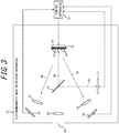
FIG. 3 is a diagram illustrating a schematic structure of the electromagnetic wave detection apparatus inFIG. 2 ; -
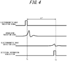
FIG. 4 is a timing chart illustrating timing of electromagnetic wave radiation and timing of electromagnetic wave detection, for explaining the principle of ranging by a ranging sensor composed of an irradiator, a second detector, and a controller; -
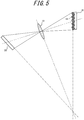
FIG. 5 is a diagram illustrating an angle-of-view range of a second image formation unit for an image formed on a first detection surface in the electromagnetic wave detection apparatus inFIG. 2 ; and -
FIG. 6 is a diagram illustrating a schematic structure of an electromagnetic wave detection apparatus according to a second embodiment. - Embodiments of an electromagnetic wave detection apparatus to which the present disclosure is applied will be described below, with reference to the drawings. As illustrated in
FIG. 1 , in a structure in which a main surface of a primary image formation optical system 15' that causes electromagnetic waves to form an image on a reference surface of a travel unit 18', the reference surface of the travel unit 18', a main surface of a secondary image formation optical system 19', and a detection surface of a detector 20' are parallel to each other, an angle-of-view range away from the main axis in the angle-of-view range of the secondary image formation optical system 19' is used for detection in some cases. Typically, in an angle-of-view range away from the main axis of an image formation system, the resolution is lower than in an angle-of-view range near the main axis (i.e. main axis neighborhood). The electromagnetic wave detection apparatus to which the present disclosure is applied is configured to use, for detection, an image of electromagnetic waves in a main axis neighborhood of the secondary image formation optical system 19'. This can improve the resolution of the image of electromagnetic waves. Hereafter, the "main axis neighborhood" refers to, on an image formation surface of an image formation optical system, a region of a predetermined range centering at the main axis of the image formation optical system. The predetermined range can be set depending on the required resolution. - An
information acquisition system 11 including an electromagneticwave detection apparatus 10 according to a first embodiment of the present disclosure includes the electromagneticwave detection apparatus 10, anirradiator 12, areflector 13, and acontrol apparatus 14, as illustrated inFIG. 2 . - In the drawings, dashed lines connecting functional blocks indicate the flow of control signals or the communication of information. Communications indicated by dashed lines may be wire communications or wireless communications. Solid lines extending from functional blocks indicate electromagnetic waves in beam form.
- The electromagnetic
wave detection apparatus 10 includes a firstimage formation unit 15, aseparator 16, atravel unit 18, a secondimage formation unit 19, afirst detector 20, a thirdimage formation unit 21, asecond detector 22, and athird detector 17, as illustrated inFIG. 3 . - The first
image formation unit 15 is located at a position facing an aperture ap formed in a housing of the electromagneticwave detection apparatus 10 so that its main axis is parallel to the axis of the aperture ap. In the case where the aperture ap is defined by a tube such as a body tube, the axis of the aperture ap is the axis of the tube. In the case where the aperture ap is formed directly in the housing, the axis of the aperture ap is a line perpendicular to the wall surface of the housing around the aperture ap and passing through the center of the aperture ap. - The first
image formation unit 15 includes, for example, at least one of a lens and a mirror. The firstimage formation unit 15 forms an image of electromagnetic waves incident from an object "ob" as a subject. The firstimage formation unit 15 may be a lens system of retrofocus type. - The
separator 16 is located between the firstimage formation unit 15 and a primary image formation position that is the position of the image of the object "ob" formed by the firstimage formation unit 15. Theseparator 16 separates electromagnetic waves incident from the firstimage formation unit 15 so as to travel in a travel unit direction da toward thetravel unit 18 and a third direction d3 toward thethird detector 17. Theseparator 16 may separate the incident electromagnetic waves so that electromagnetic waves of a first frequency travel in the travel unit direction da and electromagnetic waves of a second frequency travel in the third direction d3. - The
separator 16 separates the incident electromagnetic waves to travel in the third direction d3 and the travel unit direction da, by at least one of reflection, separation, and refraction. In the first embodiment, for example, theseparator 16 reflects a part of the incident electromagnetic waves in the third direction d3, and transmits another part of the electromagnetic waves in the travel unit direction da. For example, theseparator 16 may transmit a part of the incident electromagnetic waves in the third direction d3, and reflect another part of the electromagnetic waves in the travel unit direction da. For example, theseparator 16 may refract a part of the incident electromagnetic waves in the third direction d3, and transmit another part of the electromagnetic waves in the travel unit direction da. For example, theseparator 16 may transmit a part of the incident electromagnetic waves in the third direction d3, and refract another part of the electromagnetic waves in the travel unit direction da. For example, theseparator 16 may refract a part of the incident electromagnetic waves in the third direction d3, and refract another part of the electromagnetic waves in the travel unit direction da. - The
separator 16 may include, for example, at least one of a half mirror, a beam splitter, a dichroic mirror, a cold mirror, a hot mirror, a meta-surface, a deflection element, and a prism. - The
travel unit 18 is provided in the path of electromagnetic waves traveling in the travel unit direction da from theseparator 16. Moreover, thetravel unit 18 is located at or near the primary image formation position of the object "ob" by the firstimage formation unit 15 in the travel unit direction da. - In the first embodiment, the
travel unit 18 is provided at the primary image formation position. Thetravel unit 18 has a reference surface "ss" on which electromagnetic waves that have passed through the firstimage formation unit 15 and theseparator 16 are incident. The reference surface "ss" is composed of a plurality of pixels "px" arranged in two dimensions. The reference surface "ss" is a surface for imposing an action such as reflection or transmission on the electromagnetic waves in at least one of the below-described first state and the second state. The reference surface "ss" may be perpendicular to the central axis of electromagnetic waves traveling in the travel unit direction da from theseparator 16. - The
travel unit 18 is capable of switching each pixel "px" between the first state in which electromagnetic waves incident on the reference surface "ss" are caused to travel in a first direction d1 and the second state in which the incident electromagnetic waves are caused to travel in a second direction d2. In the first embodiment, the first state is a first reflection state in which electromagnetic waves incident on the reference surface "ss" are reflected in the first direction d1, and the second state is a second reflection state in which electromagnetic waves incident on the reference surface "ss" are reflected in the second direction d2. - More specifically, in the first embodiment, the
travel unit 18 includes, for each pixel "px", a reflective surface for reflecting electromagnetic waves. By changing the orientation of the reflective surface of each pixel "px", thetravel unit 18 can switch the pixel "px" between the first reflection state and the second reflection state. - In the first embodiment, for example, the
travel unit 18 includes a digital micromirror device (DMD). The DMD can drive each of the micro reflective surfaces of the pixels "px" constituting the reference surface "ss", to switch the reflective surface between a state of being inclined at +12° with respect to the reference surface "ss" and a state of being inclined at -12° with respect to the reference surface "ss". The reference surface "ss" is parallel to a plate surface of a substrate on which the micro reflective surfaces are placed in the DMD. - The
travel unit 18 switches each pixel "px" between the first state and the second state, based on control by the below-describedcontrol apparatus 14. For example, thetravel unit 18 can simultaneously switch some pixels "px" to the first state to cause electromagnetic waves incident on the pixels "px" to travel in the first direction d1, and switch the other pixels "px" to the second state to cause electromagnetic waves incident on the pixels "px" to travel in the second direction d2. - The second
image formation unit 19 is located in the first direction d1 from thetravel unit 18. The secondimage formation unit 19 includes, for example, at least one of a lens and a mirror. The secondimage formation unit 19 is located so that its main surface is inclined with respect to the reference surface "ss" of thetravel unit 18. The secondimage formation unit 19 may be located so that its main axis passes through the reference surface "ss" of thetravel unit 18. The secondimage formation unit 19 may be located so that its main axis passes through the center of the reference surface "ss", i.e. the centered pixel "px". The secondimage formation unit 19 forms an image of the object "ob" as electromagnetic waves for which the traveling direction has been changed by thetravel unit 18. - The
first detector 20 is located in the path of electromagnetic waves traveling in the first direction d1 from thetravel unit 18 and passing through the secondimage formation unit 19. Thefirst detector 20 is located at or near a secondary image formation position by the secondimage formation unit 19 for an image of electromagnetic waves formed on the reference surface "ss" of thetravel unit 18. Thefirst detector 20 is located so that its detection surface is inclined with respect to the reference surface "ss", i.e. so that the respective extension surfaces of the detection surface and the reference surface "ss" intersect each other. Thefirst detector 20 may be located so as to be inclined with respect to the main surface of the secondimage formation unit 19. Thefirst detector 20 is located so that the main axis of the secondimage formation unit 19 passes through the detection surface of thefirst detector 20. Thefirst detector 20 may be located so that the main axis of the secondimage formation unit 19 passes through the center of the detection surface of thefirst detector 20. - The
first detector 20 may be located so that the extension surface of the detection surface intersects the respective extension surfaces of the reference surface "ss" and the main surface of the secondimage formation unit 19 on a single straight line. Thus, the reference surface "ss", the main surface of the secondimage formation unit 19, and the detection surface of thefirst detector 20 may be arranged so as to satisfy the condition of the Scheimpflug principle. Thefirst detector 20 detects electromagnetic waves that have passed through the secondimage formation unit 19, i.e. electromagnetic waves traveling in the first direction d1. - In the first embodiment, the
first detector 20 is a passive sensor. More specifically, in the first embodiment, thefirst detector 20 includes an element array. For example, thefirst detector 20 includes an imaging element such as an image sensor or an imaging array, and captures an image formed by electromagnetic waves on the detection surface and generates image information corresponding to the imaged object "ob". - More specifically, in the first embodiment, the
first detector 20 captures an image of visible light. Thefirst detector 20 transmits the generated image information to thecontrol apparatus 14 as a signal. - The
first detector 20 may capture an image other than visible light, such as an infrared, ultraviolet, or radio wave image. Thefirst detector 20 may include a ranging sensor. With this structure, the electromagneticwave detection apparatus 10 can acquire distance information in image form from thefirst detector 20. Thefirst detector 20 may include a thermosensor or the like. With this structure, the electromagneticwave detection apparatus 10 can acquire temperature information in image form from thefirst detector 20. - The third
image formation unit 21 is located in the second direction d2 from thetravel unit 18. The thirdimage formation unit 21 includes, for example, at least one of a lens and a mirror. The thirdimage formation unit 21 is located so that its main surface is inclined with respect to the reference surface "ss" of thetravel unit 18. The thirdimage formation unit 21 may be located so that its main axis passes through the reference surface "ss" of thetravel unit 18. The thirdimage formation unit 21 may be located so that its main axis passes through the center of the reference surface "ss", i.e. the centered pixel "px". The thirdimage formation unit 21 forms an image of the object "ob" as electromagnetic waves for which the traveling direction has been changed by thetravel unit 18. - The
second detector 22 is located in the path of electromagnetic waves traveling in the second direction d2 from thetravel unit 18 and passing through the thirdimage formation unit 21. Thesecond detector 22 is located at or near a secondary image formation position by the thirdimage formation unit 21 for an image of electromagnetic waves formed on the reference surface "ss" of thetravel unit 18. Thesecond detector 22 is located so that its detection surface is inclined with respect to the reference surface "ss", i.e. so that the respective extension surfaces of the detection surface and the reference surface "ss" intersect each other. Thesecond detector 22 is located so as to be inclined with respect to the main surface of the thirdimage formation unit 21. Thesecond detector 22 may be located so that the main axis of the thirdimage formation unit 21 passes through the detection surface of thesecond detector 22. Thesecond detector 22 may be located so that the main axis of the thirdimage formation unit 21 passes through the center of the detection surface of thesecond detector 22. - The
second detector 22 may be located so that the extension surface of the detection surface intersects the respective extension surfaces of the reference surface "ss" and the main surface of the thirdimage formation unit 21 on a single straight line. Thus, the reference surface "ss", the main surface of the thirdimage formation unit 21, and the detection surface of thesecond detector 22 may be arranged so as to satisfy the condition of the Scheimpflug principle. Thesecond detector 22 detects electromagnetic waves that have passed through the thirdimage formation unit 21, i.e. electromagnetic waves traveling in the second direction d2. - In the first embodiment, the
second detector 22 is an active sensor that detects reflected waves as a result of the object "ob" reflecting electromagnetic waves emitted from theirradiator 12 to the object "ob". In the first embodiment, thesecond detector 22 detects reflected waves as a result of the object "ob" reflecting electromagnetic waves emitted from theirradiator 12 and reflected by thereflector 13 to the object "ob". Electromagnetic waves emitted from theirradiator 12 are at least one of infrared, visible light, ultraviolet, and radio waves. Thesecond detector 22 is a sensor of the same type as or a different type from thefirst detector 20, and detects electromagnetic waves of the same type as or a different type from that detected by thefirst detector 20, as described later. - More specifically, in the first embodiment, the
second detector 22 includes an element forming a ranging sensor. For example, thesecond detector 22 includes a single element such as an avalanche photodiode (APD), a photodiode (PD), a single photon avalanche diode (SPAD), a millimeter wave sensor, a sub-millimeter wave sensor, or a ranging image sensor. Thesecond detector 22 may include an element array such as an APD array, a PD array, a multi photon pixel counter (MPPC), a ranging imaging array, or a ranging image sensor. - In the first embodiment, the
second detector 22 transmits, as a signal, detection information indicating that reflected waves from the subject have been detected, to thecontrol apparatus 14. More specifically, thesecond detector 22 is an infrared sensor that detects electromagnetic waves in the infrared band. - For the
second detector 22, it is sufficient that the foregoing structure including a single element forming a ranging sensor is able to detect electromagnetic waves, and it is not necessary to form an image on its detection surface. Hence, thesecond detector 22 need not be necessarily located at or near the secondary image formation position which is the image formation position of the thirdimage formation unit 21. With this structure, thesecond detector 22 may be located anywhere in the path of electromagnetic waves traveling in the travel unit direction da from thetravel unit 18 and passing through the thirdimage formation unit 21, as long as electromagnetic waves from all angles of view can be incident on its detection surface. - The
third detector 17 is provided in the path of electromagnetic waves traveling in the third direction d3 from theseparator 16. Moreover, thethird detector 17 is located at or near the image formation position of the object "ob" by the firstimage formation unit 15 in the third direction d3 from theseparator 16. Thethird detector 17 detects electromagnetic waves traveling in the third direction d3 from theseparator 16. - In the first embodiment, the
third detector 17 is a passive sensor. More specifically, in the first embodiment, thethird detector 17 includes an element array. For example, thethird detector 17 includes an imaging element such as an image sensor or an imaging array, and captures an image formed by electromagnetic waves on the detection surface and generates image information corresponding to the imaged object "ob". - More specifically, in the first embodiment, the
third detector 17 captures an image of visible light. Thethird detector 17 transmits the generated image information to thecontrol apparatus 14 as a signal. - The
third detector 17 may capture an image other than visible light, such as an infrared, ultraviolet, or radio wave image. Thethird detector 17 may include a ranging sensor. With this structure, the electromagneticwave detection apparatus 10 can acquire distance information in image form from thethird detector 17. Thethird detector 17 may include a ranging sensor, a thermosensor, or the like. With this structure, the electromagneticwave detection apparatus 10 can acquire temperature information in image form from thethird detector 17. - The
irradiator 12 radiates at least one of infrared, visible light, ultraviolet, and radio waves. In the first embodiment, theirradiator 12 radiates infrared. Theirradiator 12 irradiates the object "ob" with the radiated electromagnetic waves either directly or indirectly through thereflector 13. In the first embodiment, theirradiator 12 irradiates the object "ob" with the radiated electromagnetic waves indirectly through thereflector 13. - In the first embodiment, the
irradiator 12 radiates electromagnetic waves of narrow width, e.g. 0.5°, in beam form. In the first embodiment, theirradiator 12 can radiate electromagnetic waves in pulse form. For example, theirradiator 12 includes a light emitting diode (LED), a laser diode (LD), and the like. Theirradiator 12 switches between radiating electromagnetic waves and stopping the radiation, based on control by the below-describedcontrol apparatus 14. - The
reflector 13 reflects the electromagnetic waves radiated from theirradiator 12 while changing the direction, to change the irradiation position at which the object "ob" is irradiated with the electromagnetic waves. That is, thereflector 13 scans the object "ob" by the electromagnetic waves radiated from theirradiator 12. Thus, in the first embodiment, thesecond detector 22 forms a scanning ranging sensor together with thereflector 13. Thereflector 13 scans the object "ob" one-dimensionally or two-dimensionally. In the first embodiment, thereflector 13 scans the object "ob" two-dimensionally. - The
reflector 13 is configured so that at least part of the irradiation region of the electromagnetic waves radiated from theirradiator 12 and reflected by thereflector 13 is included in the electromagnetic wave detection range of the electromagneticwave detection apparatus 10. Hence, at least part of the electromagnetic waves with which the object "ob" is irradiated through thereflector 13 is detectable by the electromagneticwave detection apparatus 10. - In the first embodiment, the
reflector 13 is configured so that at least part of the irradiation region of the electromagnetic waves radiated from theirradiator 12 and reflected by thereflector 13 is included in the detection range in thesecond detector 22. Hence, in the first embodiment, at least part of the electromagnetic waves with which the object "ob" is irradiated through thereflector 13 is detectable by thesecond detector 22. - The
reflector 13 includes, for example, a microelectromechanical systems (MEMS) mirror, a polygon mirror, a galvanometer mirror, or the like. In the first embodiment, thereflector 13 includes a MEMS mirror. - The
reflector 13 changes the direction in which the electromagnetic waves are reflected, based on control by the below-describedcontrol apparatus 14. For example, thereflector 13 may include an angle sensor such as an encoder, and may notify thecontrol apparatus 14 of the angle detected by the angle sensor as direction information indicating the direction in which the electromagnetic waves are reflected. With this structure, thecontrol apparatus 14 can calculate the irradiation position based on the direction information acquired from thereflector 13. Thecontrol apparatus 14 can also calculate the irradiation position based on a drive signal that is input in order to cause thereflector 13 to change the direction in which the electromagnetic waves are reflected. - The
control apparatus 14 includes one or more processors and memory. The processors may include at least one of a general-purpose processor that performs a specific function by reading a specific program and a dedicated processor dedicated to a specific process. The dedicated processor may include an application specific integrated circuit (ASIC). Each processor may include a programmable logic device (PLD). The PLD may include a field-programmable gate array (FPGA). Thecontrol apparatus 14 may include at least one of a system on a chip (SoC) and a system in a package (SiP) in which one or more processors cooperate with each other. - The
control apparatus 14 acquires information about the surroundings of the electromagneticwave detection apparatus 10, based on the electromagnetic waves detected by each of thefirst detector 20, thesecond detector 22, and thethird detector 17. Examples of the information about the surroundings include image information, distance information, and temperature information. In the first embodiment, thecontrol apparatus 14 acquires, as image information, the electromagnetic waves detected by thefirst detector 20 or thethird detector 17 as an image, as described above. In the first embodiment, thecontrol apparatus 14 acquires distance information of the irradiation position by theirradiator 12 based on the detection information of thesecond detector 22 using a time-of-flight (ToF) method, as described later. - As illustrated in
FIG. 4 , thecontrol apparatus 14 inputs an electromagnetic wave radiation signal to theirradiator 12 to cause theirradiator 12 to radiate electromagnetic waves in pulse form (see "electromagnetic wave radiation signal"). Theirradiator 12 emits electromagnetic waves based on the input electromagnetic wave radiation signal (see "irradiator radiation level"). Electromagnetic waves radiated by theirradiator 12 and reflected by thereflector 13 to be applied to a given irradiation region are reflected in the irradiation region. Thecontrol apparatus 14 switches at least some of the pixels "px" in the image formation region on thetravel unit 18 formed by the firstimage formation unit 15 from the reflected waves in the irradiation region to the first state, and the other pixels "px" to the second state. Thefirst detector 20, upon detecting the electromagnetic waves reflected in the irradiation region (see "electromagnetic wave detection level"), provides the detection information to thecontrol apparatus 14, as described above. - The
control apparatus 14 includes, for example, a time measurement LSI (large scale integrated circuit), and measures a time period ΔT from time T1 at which theirradiator 12 radiates the electromagnetic waves to time T2 at which the detection information is acquired (see "detection information acquisition"). Thecontrol apparatus 14 multiplies the time period ΔT by the speed of light and divides the result by 2, to calculate the distance to the irradiation position. Here, thecontrol apparatus 14 calculates the irradiation position based on the direction information acquired from thereflector 13 or the drive signal output from thecontrol apparatus 14 to thereflector 13, as described above. Thecontrol apparatus 14, while changing the irradiation position, calculates the distance to each irradiation position, thus generating distance information in image form. - In the first embodiment, the
information acquisition system 11 has a structure in which distance information is generated by direct ToF whereby electromagnetic waves are emitted and the time until the electromagnetic waves return is directly measured, as described above. However, theinformation acquisition system 11 is not limited to such a structure. For example, theinformation acquisition system 11 may generate distance information by flash ToF whereby electromagnetic waves are emitted at regular intervals and the time to the return is indirectly measured from the phase difference between the emitted electromagnetic waves and the returned electromagnetic waves. Theinformation acquisition system 11 may generate distance information by other ToF methods, such as phased ToF. - In the electromagnetic
wave detection apparatus 10 according to the first embodiment with the structure described above, thetravel unit 18, the secondimage formation unit 19, and thefirst detector 20 are arranged so that the respective extension surfaces of the reference surface "ss" and the detection surface of thefirst detector 20 intersect each other and the main axis of the secondimage formation unit 19 passes through the reference surface "ss" and the detection surface of thefirst detector 20. With such a structure, the reference surface "ss" of thetravel unit 18, the main surface of the secondimage formation unit 19, and the detection surface of thefirst detector 20 can be arranged so as to satisfy the condition of the Scheimpflug principle, as illustrated inFIG. 5 . Accordingly, in the electromagneticwave detection apparatus 10, even though the secondimage formation unit 19 is displaced from a position facing thetravel unit 18, an image of electromagnetic waves can be formed on the detection surface of thefirst detector 20 so that the image formed in a main axis neighborhood of the secondimage formation unit 19 for an image formed on the reference surface "ss" by the firstimage formation unit 19 be contained within the detection surface of thefirst detector 20. The electromagneticwave detection apparatus 10 can thus improve the resolution of the image of electromagnetic waves detected by thefirst detector 20. Such structures and effects also apply to the below-described electromagnetic wave detection apparatus according to a second embodiment. - The electromagnetic
wave detection apparatus 10 according to the first embodiment is capable of switching electromagnetic waves between the first state and the second state for each pixel "px". With such a structure, the electromagneticwave detection apparatus 10 can align the main axis of the firstimage formation unit 15 to the main axis of the secondimage formation unit 19 in the first direction d1 in which the electromagnetic waves travel in the first state and to the main axis of the thirdimage formation unit 21 in the second direction d2 in which the electromagnetic waves travel in the second state. Accordingly, the electromagneticwave detection apparatus 10 can reduce deviation between the main axes of thefirst detector 20 and thesecond detector 22, by switching each pixel "px" in thetravel unit 18 to the first state or the second state. The electromagneticwave detection apparatus 10 can thus reduce deviation between the coordinate systems in the detection results by thefirst detector 20 and thesecond detector 22. Such structures and effects also apply to the below-described electromagnetic wave detection apparatus according to a second embodiment. - The electromagnetic
wave detection apparatus 10 according to the first embodiment includes the thirdimage formation unit 21 and thesecond detector 22. With such a structure, the electromagneticwave detection apparatus 10 can detect information based on electromagnetic waves for each part of the object "ob" emitting electromagnetic waves incident on each pixel "px", by thesecond detector 22. Such structures and effects also apply to the below-described electromagnetic wave detection apparatus according to the second embodiment. - In the electromagnetic
wave detection apparatus 10 according to the first embodiment, thetravel unit 18, the thirdimage formation unit 21, and thesecond detector 22 are arranged so that the respective extension surfaces of the reference surface "ss", the main surface of the thirdimage formation unit 21, and the detection surface of thesecond detector 22 intersect one another on the same straight line. With such a structure, the reference surface "ss" of thetravel unit 18, the main surface of the thirdimage formation unit 21, and the detection surface of thesecond detector 22 can be arranged so as to satisfy the condition of the Scheimpflug principle. Accordingly, in the electromagneticwave detection apparatus 10, even though the thirdimage formation unit 21 is displaced from a position facing thetravel unit 18, an image of electromagnetic waves in a main axis neighborhood of the thirdimage formation unit 21 can be detected on the detection surface of thesecond detector 22. The electromagneticwave detection apparatus 10 can thus improve the resolution of the image of electromagnetic waves detected by thesecond detector 22. - The electromagnetic
wave detection apparatus 10 according to the first embodiment separates electromagnetic waves incident from the firstimage formation unit 15 to travel in the travel unit direction da and the third direction d3. With such a structure, the electromagneticwave detection apparatus 10 can align the main axis of the firstimage formation unit 15 to the central axis of electromagnetic waves traveling in the travel unit direction da and the central axis of electromagnetic waves traveling in the third direction d3. Accordingly, the electromagneticwave detection apparatus 10 can reduce deviation in coordinate system between each of thefirst detector 20 and thesecond detector 22 and thethird detector 17. Such structures and effects also apply to the below-described electromagnetic wave detection apparatus according to the second embodiment. - The electromagnetic
wave detection apparatus 10 according to the first embodiment includes thethird detector 17. With such a structure, the electromagneticwave detection apparatus 10 can additionally detect electromagnetic waves of the same image as the image formed on thefirst detector 20. Such structures and effects also apply to the below-described electromagnetic wave detection apparatus according to the second embodiment. - In the
information acquisition system 11 according to the first embodiment, thecontrol apparatus 14 acquires information about the surroundings of the electromagneticwave detection apparatus 10, based on the electromagnetic waves detected by each of thefirst detector 20, thesecond detector 22, and thethird detector 17. With such a structure, theinformation acquisition system 11 can provide useful information based on the detected electromagnetic waves. - An electromagnetic wave detection apparatus according to the second embodiment of the present disclosure will be described below. The second embodiment is different from the first embodiment in respect to the postures of the travel unit and the third detector relative to the first image formation unit and the positions and postures of the third image formation unit and the second detector relative to the travel unit. The second embodiment will be described below, mainly focusing on the differences from the first embodiment. Parts having the same structures as those in the first embodiment are given the same reference signs.
- As illustrated in
FIG. 6 , an electromagneticwave detection apparatus 100 according to the second embodiment includes a firstimage formation unit 150, aseparator 16, atravel unit 180, a secondimage formation unit 19, afirst detector 20, a thirdimage formation unit 210, asecond detector 220, and athird detector 170. Components other than the electromagneticwave detection apparatus 100 in theinformation acquisition system 11 according to the second embodiment are the same as those in the first embodiment. Theseparator 16, the secondimage formation unit 19, and thefirst detector 20 in the second embodiment have the same structures and functions as those in the first embodiment. - In the second embodiment, the first
image formation unit 150 is located so that its main axis is inclined with respect to the axis of the aperture ap and passes through the aperture ap, unlike in the first embodiment. The structure and function of the firstimage formation unit 150 are the same as those of the firstimage formation unit 150 in the first embodiment. - In the second embodiment, the
travel unit 180 is located so that the reference surface "ss" is inclined with respect to a virtual plane vp through which the main axis of the firstimage formation unit 150 passes, i.e. so that the respective extension surfaces of the virtual plane vp and the reference surface "ss" intersect each other, unlike in the first embodiment. The virtual plane vp may be a plane that is at a predetermined distance away from the firstimage formation unit 150 and is perpendicular to the axis of the aperture ap. The predetermined distance is the distance to the object surface from the firstimage formation unit 150 whose spacing to thetravel unit 180 is set and whose image surface is the reference surface "ss". - The
travel unit 180 may be located so that the respective extension surfaces of the main surface of the firstimage formation unit 150 and the reference surface "ss" of thetravel unit 180 intersect each other, i.e. so that the reference surface "ss" is inclined with respect to the main surface of the firstimage formation unit 150. In the second embodiment, in the case where the separation to the travel unit direction da by theseparator 16 is refraction, the inclination arrangement of the reference surface "ss" with respect to the main surface of the firstimage formation unit 150 means inclination arrangement, with respect to the main surface of the firstimage formation unit 150, of the reference surface "ss" of thetravel unit 180 rotated in the opposite direction of the refraction by (angle of incidence - angle of refraction) about the position of theseparator 16. In the second embodiment, in the case where the separation to the travel unit direction da by theseparator 16 is reflection, the inclination arrangement of the reference surface "ss" with respect to the main surface of the firstimage formation unit 150 means inclination arrangement, with respect to the main surface of the firstimage formation unit 150, of the reference surface "ss" in a plane-symmetrical posture on the reflective surface of theseparator 16. - The
travel unit 180 is located so that the main axis of the firstimage formation unit 150 passes through the reference surface "ss" of thetravel unit 180. Thetravel unit 180 may be located so that the main axis of the firstimage formation unit 150 passes through the center of the reference surface "ss" of thetravel unit 180. - The
travel unit 180 may be located so that the extension surface of the reference surface "ss" intersects the main surface of the firstimage formation unit 150 and virtual plane vp on a single straight line. Thus, the main surface of the firstimage formation unit 150, the reference surface "ss", and the virtual plane vp are arranged so as to satisfy the condition of the Scheimpflug principle. - In the second embodiment, the
travel unit 180 may be located so that a second direction d2 as a direction of travel by thetravel unit 180 is perpendicular to the reference surface "ss". The structure and function of thetravel unit 180 other than the posture described above are the same as those of thetravel unit 18 in the first embodiment. - In the second embodiment, the second
image formation unit 19 is located in a first direction d1 as a direction of travel by thetravel unit 180 so that its main surface is inclined with respect to the reference surface "ss" of thetravel unit 180, as in the first embodiment. The other arrangement condition, structure, and function of the secondimage formation unit 19 in the second embodiment are the same as those of the secondimage formation unit 19 in the first embodiment. - In the second embodiment, the
first detector 20 is located at or near a secondary image formation position by the secondimage formation unit 19 for an image of electromagnetic waves formed on the reference surface "ss" of thetravel unit 18, as in the first embodiment. In the second embodiment, thefirst detector 20 is located so that the extension surface of the detection surface intersects the respective extension surfaces of the reference surface "ss" and the main surface of the secondimage formation unit 19 on a single straight line, as in the first embodiment. Thus, in the second embodiment, too, the reference surface "ss", the main surface of the secondimage formation unit 19, and the detection surface of thefirst detector 20 are arranged so as to satisfy the condition of the Scheimpflug principle, as in the first embodiment. The other arrangement condition, structure, and function of thefirst detector 20 in the second embodiment are the same as those of thefirst detector 20 in the first embodiment. - In the second embodiment, the third
image formation unit 210 is located so that its main surface is parallel to the reference surface "ss" of thetravel unit 18, unlike in the first embodiment. The other arrangement condition, structure, and function of the thirdimage formation unit 210 in the second embodiment are the same as those of the thirdimage formation unit 21 in the first embodiment. - In the second embodiment, the
second detector 220 is located so that its detection surface is perpendicular to the main axis of the thirdimage formation unit 210, unlike in the first embodiment. The other arrangement condition, structure, and function of thesecond detector 220 in the second embodiment are the same as those of thesecond detector 22 in the first embodiment. - In the second embodiment, the
third detector 170 is located so that the respective extension surfaces of the main surface of the firstimage formation unit 150 and the detection surface of thethird detector 170 intersect each other, i.e. so that the detection surface is inclined with respect to the main surface of the firstimage formation unit 150, unlike in the first embodiment. In the second embodiment, in the case where the separation to the third direction d3 by theseparator 16 is refraction, the inclination arrangement of the detection surface with respect to the main surface of the firstimage formation unit 150 means inclination arrangement, with respect to the main surface of the firstimage formation unit 150, of the detection surface of thethird detector 170 rotated in the opposite direction of the refraction by (angle of incidence - angle of refraction) about the position of theseparator 16. In the second embodiment, in the case where the separation to the third direction d3 by theseparator 16 is reflection, the inclination arrangement of the detection surface with respect to the main surface of the firstimage formation unit 150 means inclination arrangement, with respect to the main surface of the firstimage formation unit 150, of the detection surface in a plane-symmetrical posture on the reflective surface of theseparator 16. - The
third detector 170 and the firstimage formation unit 150 are arranged so that the respective extension surfaces of the main surface of the firstimage formation unit 150 and the detection surface of thethird detector 170 intersect each other on the virtual plane vp. Thus, the main surface of the firstimage formation unit 150, the detection surface of thethird detector 170, and the virtual plane vp are arranged so as to satisfy the condition of the Scheimpflug principle. The other arrangement condition, structure, and function of thethird detector 170 in the second embodiment are the same as those of thethird detector 17 in the first embodiment. - As described above, in the electromagnetic
wave detection apparatus 100 according to the second embodiment, the firstimage formation unit 150 and thetravel unit 180 are arranged so that the respective extension surfaces of the virtual plane vp through which the main axis of the firstimage formation unit 150 passes and the reference surface "ss" of thetravel unit 180 intersect each other and the main axis of the firstimage formation unit 150 passes through the reference surface "ss". With such a structure, the virtual plane vp at the predetermined distance away from the firstimage formation unit 150, the main surface of the firstimage formation unit 150, and the reference surface "ss" of thetravel unit 180, and the main surface of the secondimage formation unit 19 and the detection surface of thefirst detector 20 are arranged so as to satisfy the condition of the Scheimpflug principle. Thus, in the electromagneticwave detection apparatus 10, even with the structure in which the firstimage formation unit 150 is not located at a position facing thetravel unit 180, an image of electromagnetic waves can be formed on the reference surface "ss" of thetravel unit 180 so that the image formed in a main axis neighborhood by the firstimage formation unit 150 for the object on the virtual plane through which the main axis of the firstimage formation unit 150 passes can be contained within the reference surface "ss" of thetravel unit 180 . Therefore, in the electromagneticwave detection apparatus 10, the thirdimage formation unit 210 can be located at a position facing thetravel unit 180. Consequently, while the reference surface "ss" of thetravel unit 180 and the main surface of the thirdimage formation unit 210 are parallel to each other, the thirdimage formation unit 210 can be located so that the main axis of the thirdimage formation unit 210 passes through the reference surface "ss" of thetravel unit 180. With such arrangement, the electromagneticwave detection apparatus 10 can form an image of an angle-of-view range in a main axis neighborhood of the thirdimage formation unit 210 on thesecond detector 220, so that the resolution of the image of electromagnetic waves detected by thesecond detector 220 can be improved. - While some embodiments of the present disclosure have been described above with reference to the drawings, various changes or modifications may be easily made by those of ordinary skill in the art based on the present disclosure. Such various changes or modifications are therefore included in the scope of the present disclosure.
- For example, although the
irradiator 12, thereflector 13, and thecontrol apparatus 14 constitute theinformation acquisition system 11 together with the electromagneticwave detection apparatus wave detection apparatus irradiator 12, thereflector 13, and thecontrol apparatus 14. For example, the electromagneticwave detection apparatus control apparatus 14 as a controller. - Although the
travel unit - Although the first state and the second state in the
travel unit travel unit - For example, the first state may be a passing state in which electromagnetic waves incident on the reference surface "ss" are allowed to pass to travel in the first direction d1. More specifically, the
travel unit travel unit travel unit - The
travel unit travel unit - Although the
information acquisition system 11 in each of the first and second embodiments has a structure in which thesecond detector reflector 13 that scans the object with electromagnetic waves in beam form radiated from theirradiator 12, theinformation acquisition system 11 is not limited to such a structure. For example, even in the case where theinformation acquisition system 11 does not include thereflector 13 and radiates radial electromagnetic waves from theirradiator 12 and acquires information without scanning, effects similar to those of the first embodiment can be achieved. - Although the
information acquisition system 11 in each of the first and second embodiments has a structure in which thefirst detector 20 and thethird detector second detector 220 is an active sensor, theinformation acquisition system 11 is not limited to such a structure. For example, even in the case where thefirst detector 20, thesecond detector third detector first detector 20, thesecond detector third detector information acquisition system 11, effects similar to those of the first and second embodiments can be achieved. - It should be noted that the system is disclosed herein as having various modules and/or units for executing specific functions. These modules and units are schematically illustrated to simplify the description of its functionality, and do not necessarily represent specific hardware and/or software. In this regard, the modules, units, and other components may be hardware and/or software implemented to substantially execute the specific functions described herein. Various functions of different components may be any combination or separate ones of hardware and/or software, and may be used separately or in combination. Input/output (I/O) devices or user interfaces including, but not limited to, a keyboard, a display, a touchscreen, and a pointing device may be connected to the system directly or via intervening I/O controllers. Thus, the disclosed various aspects may be embodied in many different forms, and all such embodiments are within the scope of the present disclosure.
-
- 10, 100
- electromagnetic wave detection apparatus
- 11
- information acquisition system
- 12
- irradiator
- 13
- reflector
- 14
- control apparatus
- 15
- first image formation unit
- 15'
- primary image formation optical system
- 16
- separator
- 17
- third detector
- 18, 180
- travel unit
- 18'
- travel unit
- 19
- second image formation unit
- 19'
- secondary image formation optical system
- 20
- first detector
- 20'
- detector
- 21
- third image formation unit
- 22
- second detector
- ap
- aperture
- da
- travel unit direction
- d1, d2, d3
- first direction, second direction, third direction
- ob
- object
- px
- pixel
- ss
- action surface
- vp
- virtual plane
Claims (40)
- An electromagnetic wave detection apparatus comprising:a first image formation unit configured to form an image of incident electromagnetic waves;a travel unit including a plurality of pixels arranged along a reference surface, and configured to cause electromagnetic waves incident on the reference surface from the first image formation unit to travel in a first direction for each of the plurality of pixels;a second image formation unit configured to form an image of electromagnetic waves traveling in the first direction; anda first detector configured to detect electromagnetic waves incident from the second image formation unit,wherein the electromagnetic wave detection apparatus has at least one of: an arrangement in which respective extension surfaces of the reference surface and a detection surface of the first detector intersect each other and a main axis of the second image formation unit passes through the reference surface and the detection surface of the first detector; and an arrangement in which respective extension surfaces of the reference surface and an object surface of the first image formation unit intersect each other, and a main axis of the first image formation unit passes through the reference surface, wherein the first image information unit sets spacing to the travel unit ant an image surface of the first image formation unit is on the reference surface.
- The electromagnetic wave detection apparatus according to claim 1, having at least one of: an arrangement in which the main axis of the second image formation unit passes through a center of the reference surface and a center of the detection surface of the first detector; and an arrangement in which the main axis of the first image formation unit passes through the center of the reference surface.
- The electromagnetic wave detection apparatus according to claim 1 or 2, having at least one of: an arrangement in which respective extension surfaces of the reference surface, a main surface of the second image formation unit, and the detection surface of the first detector intersect one another on a same straight line; and an arrangement in which respective extension surfaces of the reference surface and a main surface of the first image formation unit intersect each other.
- The electromagnetic wave detection apparatus according to any one of claims 1 to 3, having at least one of: an arrangement in which the reference surface, a main surface of the second image formation unit, and the detection surface of the first detector satisfy a condition of Scheimpflug principle; and an arrangement in which a main surface of the first image formation unit and the reference surface satisfy the condition of Scheimpflug principle.
- The electromagnetic wave detection apparatus according to any one of claims 1 to 4, wherein the travel unit is configured to switch each of the plurality of pixels between a first state in which the electromagnetic waves incident on the reference surface from the first image formation unit are caused to travel in the first direction and a second state in which the electromagnetic waves are caused to travel in a second direction.
- The electromagnetic wave detection apparatus according to claim 5, further comprising:a third image formation unit configured to form an image of electromagnetic waves traveling in the second direction; anda second detector configured to detect electromagnetic waves incident from the third image formation unit.
- The electromagnetic wave detection apparatus according to claim 6, having an arrangement in which respective extension surfaces of the reference surface and a detection surface of the second detector intersect each other and a main axis of the third image formation unit passes through the reference surface and the detection surface of the second detector.
- The electromagnetic wave detection apparatus according to claim 6 or 7, having an arrangement in which a main axis of the third image formation unit passes through a center of the reference surface and a center of a detection surface of the second detector.
- The electromagnetic wave detection apparatus according to any one of claims 6 to 8, having an arrangement in which respective extension surfaces of the reference surface, a main surface of the third image formation unit, and a detection surface of the second detector intersect one another on a same straight line.
- The electromagnetic wave detection apparatus according to any one of claims 6 to 9, having an arrangement in which the reference surface, a main surface of the third image formation unit, and a detection surface of the second detector satisfy a condition of Scheimpflug principle.
- The electromagnetic wave detection apparatus according to any one of claims 7 to 10, wherein the travel unit includes a reflective surface for each of the plurality of pixels, and is configured to change an orientation of the reflective surface of each of the plurality of pixels.
- The electromagnetic wave detection apparatus according to claim 11, wherein the travel unit is configured to switch each of the plurality of pixels between the first state and the second state by changing the orientation of the reflective surface of the pixel.
- The electromagnetic wave detection apparatus according to claim 12, wherein the travel unit includes a digital micromirror device in which a plurality of mirrors are arranged on a plane, and is configured to switch each of the plurality of pixels between the first state and the second state by changing an orientation of a corresponding mirror of the digital micromirror device for the pixel.
- The electromagnetic wave detection apparatus according to any one of claims 7 to 10, wherein the travel unit includes a reflective surface for each of the plurality of pixels, and is configured to open and close the reflective surface of each of the plurality of pixels.
- The electromagnetic wave detection apparatus according to claim 14, wherein the travel unit is configured to switch each of the plurality of pixels between the first state and the second state by opening or closing the reflective surface of the pixel.
- The electromagnetic wave detection apparatus according to claim 15, wherein the travel unit includes a MEMS shutter in which a plurality of shutters each capable of opening and closing the reflective surface of a corresponding one of the plurality of pixels are arranged on a plane, and is configured to switch each of the plurality of pixels between the first state and the second state by opening or closing a corresponding shutter of the MEMS shutter.
- The electromagnetic wave detection apparatus according to any one of claims 7 to 10, wherein the travel unit is configured to switch each of the plurality of pixels between a reflection state in which the electromagnetic waves are reflected and a transmission state in which the electromagnetic waves are transmitted, depending on a liquid crystal orientation.
- The electromagnetic wave detection apparatus according to claim 17, wherein the travel unit is configured to switch each of the plurality of pixels between the first state and the second state by switching the pixel between the reflection state and the transmission state depending on the liquid crystal orientation.
- The electromagnetic wave detection apparatus according to claim 18, wherein the travel unit includes a liquid crystal shutter capable of switching between the reflection state and the transmission state depending on the liquid crystal orientation, and is configured to switch each of the plurality of pixels between the first state and the second state by switching the liquid crystal orientation of the liquid crystal shutter.
- The electromagnetic wave detection apparatus according to any one of claims 1 to 19, wherein the first detector includes at least one of a PD, an APD, an SPAD, an MPPC, an image sensor, an infrared sensor, a millimeter wave sensor, a sub-millimeter wave sensor, a ranging image sensor, a ranging sensor, and a thermosensor.
- The electromagnetic wave detection apparatus according to any one of claims 1 to 20, wherein the first detector is configured to detect at least one of infrared, visible light, ultraviolet, and radio waves.
- The electromagnetic wave detection apparatus according to claim 8, wherein the second detector includes a sensor of a same type as or a different type from the first detector.
- The electromagnetic wave detection apparatus according to any one of claims 1 to 22, further comprising
a separator configured to separate electromagnetic waves incident from the first image formation unit, to travel in a direction toward the travel unit and a third direction. - The electromagnetic wave detection apparatus according to claim 23, wherein the separator is configured to separate the electromagnetic waves incident from the first image formation unit so that electromagnetic waves of a first frequency travel in the direction toward the travel unit and electromagnetic waves of a second frequency travel in the third direction.
- The electromagnetic wave detection apparatus according to claim 23 or 24, wherein the separator is configured to separate the incident electromagnetic waves to travel in the direction toward the travel unit and the third direction, by at least one of reflection, transmission, and refraction.
- The electromagnetic wave detection apparatus according to any one of claims 23 to 25, wherein the separator is configured to transmit a part of the incident electromagnetic waves in the direction toward the travel unit and reflect another part of the incident electromagnetic waves in the third direction.
- The electromagnetic wave detection apparatus according to any one of claims 23 to 25, wherein the separator is configured to reflect a part of the incident electromagnetic waves in the direction toward the travel unit and transmit another part of the incident electromagnetic waves in the third direction.
- The electromagnetic wave detection apparatus according to any one of claims 23 to 25, wherein the separator is configured to transmit a part of the incident electromagnetic waves in the direction toward the travel unit and refract another part of the incident electromagnetic waves in the third direction.
- The electromagnetic wave detection apparatus according to any one of claims 23 to 25, wherein the separator is configured to refract a part of the incident electromagnetic waves in the direction toward the travel unit and transmit another part of the incident electromagnetic waves in the third direction.
- The electromagnetic wave detection apparatus according to any one of claims 23 to 25, wherein the separator is configured to refract a part of the incident electromagnetic waves in the direction toward the travel unit and refract another part of the incident electromagnetic waves in the third direction.
- The electromagnetic wave detection apparatus according to any one of claims 23 to 30, wherein the separator includes at least one of a half mirror, a beam splitter, a dichroic mirror, a cold mirror, a hot mirror, a meta-surface, a deflection element, and a prism.
- The electromagnetic wave detection apparatus according to any one of claims 23 to 31, further comprising
a third detector configured to detect electromagnetic waves traveling in the third direction. - The electromagnetic wave detection apparatus according to any one of claims 1 to 32, wherein the first image formation unit is a lens system of retrofocus type.
- The electromagnetic wave detection apparatus according to any one of claims 1 to 33, further comprising
a controller configured to acquire information about surroundings based on the electromagnetic waves detected by the first detector. - The electromagnetic wave detection apparatus according to claim 8, further comprising
a controller configured to acquire information about surroundings based on the electromagnetic waves detected by the second detector. - The electromagnetic wave detection apparatus according to claim 32, further comprising
a controller configured to acquire information about surroundings based on the electromagnetic waves detected by the third detector. - An information acquisition system comprising:the electromagnetic wave detection apparatus according to any one of claims 1 to 33; anda control apparatus configured to acquire information about surroundings of the electromagnetic wave detection apparatus based on the electromagnetic waves detected by the first detector.
- An information acquisition system comprising:the electromagnetic wave detection apparatus according to claim 6; anda control apparatus configured to acquire information about surroundings of the electromagnetic wave detection apparatus based on the electromagnetic waves detected by the second detector.
- An information acquisition system comprising:the electromagnetic wave detection apparatus according to claim 32; anda control apparatus configured to acquire information about surroundings of the electromagnetic wave detection apparatus based on the electromagnetic waves detected by the third detector.
- An electromagnetic wave detection apparatus comprising:a first image formation unit configured to form an image of incident electromagnetic waves;a travel unit including a plurality of pixels arranged along a reference surface, and configured to cause electromagnetic waves incident on the reference surface from the first image formation unit to travel in a first direction for each of the plurality of pixels;a second image formation unit configured to form an image of electromagnetic waves traveling in the first direction; anda first detector configured to detect electromagnetic waves incident from the second image formation unit,wherein the electromagnetic wave detection apparatus has at least one of: an arrangement in which an image formed in a main axis neighborhood by the second image formation unit for an image formed on the reference surface by the first image formation unit is contained within a detection surface of the first detector; and an arrangement in which an image formed in a main axis neighborhood by the first image formation unit for an object through which a main axis of the first image formation unit passes is contained within the reference surface.
Applications Claiming Priority (2)
| Application Number | Priority Date | Filing Date | Title |
|---|---|---|---|
| JP2018011881A JP7025940B2 (en) | 2018-01-26 | 2018-01-26 | Electromagnetic wave detection device and information acquisition system |
| PCT/JP2019/001035 WO2019146461A1 (en) | 2018-01-26 | 2019-01-16 | Electromagnetic wave detection device and information acquisition system |
Publications (2)
| Publication Number | Publication Date |
|---|---|
| EP3745708A1 true EP3745708A1 (en) | 2020-12-02 |
| EP3745708A4 EP3745708A4 (en) | 2021-09-22 |
Family
ID=67395458
Family Applications (1)
| Application Number | Title | Priority Date | Filing Date |
|---|---|---|---|
| EP19743191.9A Pending EP3745708A4 (en) | 2018-01-26 | 2019-01-16 | ELECTROMAGNETIC WAVE DETECTION DEVICE AND INFORMATION ACQUISITION SYSTEM |
Country Status (5)
| Country | Link |
|---|---|
| US (1) | US11573316B2 (en) |
| EP (1) | EP3745708A4 (en) |
| JP (1) | JP7025940B2 (en) |
| CN (1) | CN111527740B (en) |
| WO (1) | WO2019146461A1 (en) |
Families Citing this family (3)
| Publication number | Priority date | Publication date | Assignee | Title |
|---|---|---|---|---|
| EP4276495A4 (en) * | 2021-02-02 | 2024-03-06 | Huawei Technologies Co., Ltd. | Detection device, control method, fusion detection system, and terminal |
| JP7659450B2 (en) * | 2021-06-16 | 2025-04-09 | 日本放送協会 | Imaging device and imaging method |
| CN118604835A (en) * | 2022-08-11 | 2024-09-06 | 天津市特种设备监督检验技术研究院(天津市特种设备事故应急调查处理中心) | A method for detecting the natural sliding amount of forklift forks based on laser reflection |
Family Cites Families (20)
| Publication number | Priority date | Publication date | Assignee | Title |
|---|---|---|---|---|
| JPS507865B1 (en) | 1970-05-19 | 1975-03-29 | ||
| JPH04196878A (en) * | 1990-11-28 | 1992-07-16 | Hitachi Ltd | Automatic tilting device for video camera |
| US6057909A (en) * | 1995-06-22 | 2000-05-02 | 3Dv Systems Ltd. | Optical ranging camera |
| JP3733228B2 (en) * | 1997-12-25 | 2006-01-11 | キヤノン株式会社 | Imaging device with tilt mechanism, method, and storage medium |
| EP1102104A2 (en) | 1999-11-17 | 2001-05-23 | Lucent Technologies Inc. | Optical switch |
| JP3507865B2 (en) | 2001-02-02 | 2004-03-15 | 和歌山大学長 | Method and apparatus for real-time shape measurement by CCD camera using DMD |
| JP4297630B2 (en) * | 2001-04-25 | 2009-07-15 | 株式会社リコー | Electronic imaging device |
| US8675119B2 (en) | 2001-08-09 | 2014-03-18 | Trustees Of Columbia University In The City Of New York | Adaptive imaging using digital light processing |
| CN100352264C (en) * | 2003-02-25 | 2007-11-28 | 松下电器产业株式会社 | Optical sensor |
| CN1670791B (en) * | 2004-02-12 | 2010-11-10 | 精工爱普生株式会社 | Optical display device and image display method |
| DE102005049471B4 (en) * | 2005-10-13 | 2007-09-13 | Ingenieurbüro Spies GbR (vertretungsberechtigte Gesellschafter: Hans Spies, Martin Spies, 86558 Hohenwart) | Distance sensor with single surface scan |
| WO2009133849A1 (en) * | 2008-04-28 | 2009-11-05 | 株式会社ニコン | Inspection device |
| JP2010085472A (en) * | 2008-09-29 | 2010-04-15 | Hitachi Ltd | Image projection/imaging apparatus |
| JP2011239259A (en) * | 2010-05-12 | 2011-11-24 | Sony Corp | Image processing device, image processing method, and program |
| JP5932343B2 (en) * | 2012-01-13 | 2016-06-08 | エイチエスティ・ビジョン株式会社 | Observation equipment |
| US20140043610A1 (en) * | 2012-08-07 | 2014-02-13 | Carl Zeiss Industrielle Messtechnik Gmbh | Apparatus for inspecting a measurement object with triangulation sensor |
| JP2014143383A (en) * | 2012-12-27 | 2014-08-07 | Nikon Corp | Surface position detector, exposure device, and method of manufacturing device |
| US20140192187A1 (en) * | 2013-01-08 | 2014-07-10 | Faro Technologies, Inc. | Non-contact measurement device |
| CN106464858B (en) * | 2014-04-26 | 2019-08-20 | 泰特拉维公司 | Methods and systems for durable and extended illumination waveforms for depth sensing in 3D imaging |
| EP3210372B1 (en) * | 2014-10-21 | 2023-07-19 | University College Cork-National University of Ireland, Cork | Smart photonic imaging method and apparatus |
-
2018
- 2018-01-26 JP JP2018011881A patent/JP7025940B2/en active Active
-
2019
- 2019-01-16 CN CN201980006851.8A patent/CN111527740B/en active Active
- 2019-01-16 EP EP19743191.9A patent/EP3745708A4/en active Pending
- 2019-01-16 WO PCT/JP2019/001035 patent/WO2019146461A1/en not_active Ceased
- 2019-01-16 US US16/959,106 patent/US11573316B2/en active Active
Also Published As
| Publication number | Publication date |
|---|---|
| JP2019129510A (en) | 2019-08-01 |
| CN111527740A (en) | 2020-08-11 |
| US11573316B2 (en) | 2023-02-07 |
| WO2019146461A1 (en) | 2019-08-01 |
| US20200333458A1 (en) | 2020-10-22 |
| EP3745708A4 (en) | 2021-09-22 |
| CN111527740B (en) | 2022-09-20 |
| JP7025940B2 (en) | 2022-02-25 |
Similar Documents
| Publication | Publication Date | Title |
|---|---|---|
| US12313783B2 (en) | Electromagnetic wave detection apparatus and information acquisition system | |
| US11675052B2 (en) | Electromagnetic wave detection apparatus, program, and electromagnetic wave detection system | |
| US11947068B2 (en) | Electromagnetic wave detection apparatus and information acquisition system | |
| US11573316B2 (en) | Electromagnetic wave detection apparatus and information acquisition system | |
| WO2019220978A1 (en) | Electromagnetic wave detection device and information acquisition system | |
| JP7260966B2 (en) | Electromagnetic wave detector | |
| WO2019159933A1 (en) | Electromagnetic wave detection device and information acquisition system | |
| WO2020105419A1 (en) | Electromagnetic wave detection device and information acquisition system | |
| EP3795963B1 (en) | Electromagnetic wave detection device and information acquisition system | |
| JP2020073894A (en) | Electromagnetic wave detection device and information acquisition system | |
| JP2020073895A (en) | Electromagnetic wave detection device and information acquisition system |
Legal Events
| Date | Code | Title | Description |
|---|---|---|---|
| STAA | Information on the status of an ep patent application or granted ep patent |
Free format text: STATUS: THE INTERNATIONAL PUBLICATION HAS BEEN MADE |
|
| PUAI | Public reference made under article 153(3) epc to a published international application that has entered the european phase |
Free format text: ORIGINAL CODE: 0009012 |
|
| STAA | Information on the status of an ep patent application or granted ep patent |
Free format text: STATUS: REQUEST FOR EXAMINATION WAS MADE |
|
| 17P | Request for examination filed |
Effective date: 20200619 |
|
| AK | Designated contracting states |
Kind code of ref document: A1 Designated state(s): AL AT BE BG CH CY CZ DE DK EE ES FI FR GB GR HR HU IE IS IT LI LT LU LV MC MK MT NL NO PL PT RO RS SE SI SK SM TR |
|
| AX | Request for extension of the european patent |
Extension state: BA ME |
|
| DAV | Request for validation of the european patent (deleted) | ||
| DAX | Request for extension of the european patent (deleted) | ||
| REG | Reference to a national code |
Ref country code: DE Ref legal event code: R079 Free format text: PREVIOUS MAIN CLASS: H04N0005300000 Ipc: G01S0007481000 |
|
| A4 | Supplementary search report drawn up and despatched |
Effective date: 20210823 |
|
| RIC1 | Information provided on ipc code assigned before grant |
Ipc: H04N 5/225 20060101ALI20210817BHEP Ipc: G02B 26/08 20060101ALI20210817BHEP Ipc: G01J 5/08 20060101ALI20210817BHEP Ipc: G01J 5/00 20060101ALI20210817BHEP Ipc: G01S 17/08 20060101ALI20210817BHEP Ipc: G01S 17/42 20060101ALI20210817BHEP Ipc: G01S 17/89 20200101ALI20210817BHEP Ipc: G01S 7/481 20060101AFI20210817BHEP |
|
| P01 | Opt-out of the competence of the unified patent court (upc) registered |
Effective date: 20230508 |
|
| STAA | Information on the status of an ep patent application or granted ep patent |
Free format text: STATUS: EXAMINATION IS IN PROGRESS |
|
| 17Q | First examination report despatched |
Effective date: 20250107 |