EP3745664A1 - Method and system for aligning signals widely spaced in frequency for wideband digital predistortion in wireless communication systems - Google Patents
Method and system for aligning signals widely spaced in frequency for wideband digital predistortion in wireless communication systems Download PDFInfo
- Publication number
- EP3745664A1 EP3745664A1 EP20186758.7A EP20186758A EP3745664A1 EP 3745664 A1 EP3745664 A1 EP 3745664A1 EP 20186758 A EP20186758 A EP 20186758A EP 3745664 A1 EP3745664 A1 EP 3745664A1
- Authority
- EP
- European Patent Office
- Prior art keywords
- delay
- function
- timing error
- signals
- feedback
- Prior art date
- Legal status (The legal status is an assumption and is not a legal conclusion. Google has not performed a legal analysis and makes no representation as to the accuracy of the status listed.)
- Withdrawn
Links
- 238000000034 method Methods 0.000 title claims description 51
- 238000004891 communication Methods 0.000 title description 6
- 230000003044 adaptive effect Effects 0.000 claims abstract description 9
- 238000005070 sampling Methods 0.000 claims description 7
- 238000001914 filtration Methods 0.000 claims description 5
- 238000005314 correlation function Methods 0.000 claims description 2
- 238000010586 diagram Methods 0.000 description 4
- 230000008901 benefit Effects 0.000 description 3
- 238000013461 design Methods 0.000 description 3
- 238000004364 calculation method Methods 0.000 description 2
- 239000000969 carrier Substances 0.000 description 2
- 238000006243 chemical reaction Methods 0.000 description 2
- 238000005516 engineering process Methods 0.000 description 2
- 238000012986 modification Methods 0.000 description 2
- 230000004048 modification Effects 0.000 description 2
- 230000008569 process Effects 0.000 description 2
- 238000012545 processing Methods 0.000 description 2
- 230000003595 spectral effect Effects 0.000 description 2
- 230000008859 change Effects 0.000 description 1
- 238000007796 conventional method Methods 0.000 description 1
- 230000001934 delay Effects 0.000 description 1
- 230000000694 effects Effects 0.000 description 1
- 238000010295 mobile communication Methods 0.000 description 1
- 230000009467 reduction Effects 0.000 description 1
Images

Classifications
-
- H—ELECTRICITY
- H03—ELECTRONIC CIRCUITRY
- H03F—AMPLIFIERS
- H03F1/00—Details of amplifiers with only discharge tubes, only semiconductor devices or only unspecified devices as amplifying elements
- H03F1/32—Modifications of amplifiers to reduce non-linear distortion
- H03F1/3241—Modifications of amplifiers to reduce non-linear distortion using predistortion circuits
- H03F1/3247—Modifications of amplifiers to reduce non-linear distortion using predistortion circuits using feedback acting on predistortion circuits
-
- H—ELECTRICITY
- H03—ELECTRONIC CIRCUITRY
- H03F—AMPLIFIERS
- H03F1/00—Details of amplifiers with only discharge tubes, only semiconductor devices or only unspecified devices as amplifying elements
- H03F1/32—Modifications of amplifiers to reduce non-linear distortion
- H03F1/3241—Modifications of amplifiers to reduce non-linear distortion using predistortion circuits
- H03F1/3258—Modifications of amplifiers to reduce non-linear distortion using predistortion circuits based on polynomial terms
-
- H—ELECTRICITY
- H03—ELECTRONIC CIRCUITRY
- H03F—AMPLIFIERS
- H03F3/00—Amplifiers with only discharge tubes or only semiconductor devices as amplifying elements
- H03F3/189—High-frequency amplifiers, e.g. radio frequency amplifiers
-
- H—ELECTRICITY
- H03—ELECTRONIC CIRCUITRY
- H03F—AMPLIFIERS
- H03F3/00—Amplifiers with only discharge tubes or only semiconductor devices as amplifying elements
- H03F3/20—Power amplifiers, e.g. Class B amplifiers, Class C amplifiers
- H03F3/24—Power amplifiers, e.g. Class B amplifiers, Class C amplifiers of transmitter output stages
- H03F3/245—Power amplifiers, e.g. Class B amplifiers, Class C amplifiers of transmitter output stages with semiconductor devices only
-
- H—ELECTRICITY
- H04—ELECTRIC COMMUNICATION TECHNIQUE
- H04L—TRANSMISSION OF DIGITAL INFORMATION, e.g. TELEGRAPHIC COMMUNICATION
- H04L25/00—Baseband systems
- H04L25/02—Details ; arrangements for supplying electrical power along data transmission lines
- H04L25/03—Shaping networks in transmitter or receiver, e.g. adaptive shaping networks
- H04L25/03006—Arrangements for removing intersymbol interference
- H04L25/03012—Arrangements for removing intersymbol interference operating in the time domain
- H04L25/03019—Arrangements for removing intersymbol interference operating in the time domain adaptive, i.e. capable of adjustment during data reception
- H04L25/03057—Arrangements for removing intersymbol interference operating in the time domain adaptive, i.e. capable of adjustment during data reception with a recursive structure
- H04L25/03063—Arrangements for removing intersymbol interference operating in the time domain adaptive, i.e. capable of adjustment during data reception with a recursive structure using fractionally spaced delay lines or combinations of fractionally and integrally spaced taps
-
- H—ELECTRICITY
- H04—ELECTRIC COMMUNICATION TECHNIQUE
- H04L—TRANSMISSION OF DIGITAL INFORMATION, e.g. TELEGRAPHIC COMMUNICATION
- H04L43/00—Arrangements for monitoring or testing data switching networks
- H04L43/02—Capturing of monitoring data
- H04L43/028—Capturing of monitoring data by filtering
-
- H—ELECTRICITY
- H03—ELECTRONIC CIRCUITRY
- H03F—AMPLIFIERS
- H03F2200/00—Indexing scheme relating to amplifiers
- H03F2200/336—A I/Q, i.e. phase quadrature, modulator or demodulator being used in an amplifying circuit
-
- H—ELECTRICITY
- H03—ELECTRONIC CIRCUITRY
- H03F—AMPLIFIERS
- H03F2200/00—Indexing scheme relating to amplifiers
- H03F2200/451—Indexing scheme relating to amplifiers the amplifier being a radio frequency amplifier
-
- H—ELECTRICITY
- H04—ELECTRIC COMMUNICATION TECHNIQUE
- H04L—TRANSMISSION OF DIGITAL INFORMATION, e.g. TELEGRAPHIC COMMUNICATION
- H04L25/00—Baseband systems
- H04L25/02—Details ; arrangements for supplying electrical power along data transmission lines
- H04L25/03—Shaping networks in transmitter or receiver, e.g. adaptive shaping networks
- H04L25/03006—Arrangements for removing intersymbol interference
- H04L25/03343—Arrangements at the transmitter end
-
- H—ELECTRICITY
- H04—ELECTRIC COMMUNICATION TECHNIQUE
- H04L—TRANSMISSION OF DIGITAL INFORMATION, e.g. TELEGRAPHIC COMMUNICATION
- H04L27/00—Modulated-carrier systems
- H04L27/0002—Modulated-carrier systems analog front ends; means for connecting modulators, demodulators or transceivers to a transmission line
-
- H—ELECTRICITY
- H04—ELECTRIC COMMUNICATION TECHNIQUE
- H04L—TRANSMISSION OF DIGITAL INFORMATION, e.g. TELEGRAPHIC COMMUNICATION
- H04L27/00—Modulated-carrier systems
- H04L27/26—Systems using multi-frequency codes
- H04L27/2601—Multicarrier modulation systems
- H04L27/2626—Arrangements specific to the transmitter only
- H04L27/2627—Modulators
-
- H—ELECTRICITY
- H04—ELECTRIC COMMUNICATION TECHNIQUE
- H04L—TRANSMISSION OF DIGITAL INFORMATION, e.g. TELEGRAPHIC COMMUNICATION
- H04L27/00—Modulated-carrier systems
- H04L27/26—Systems using multi-frequency codes
- H04L27/2601—Multicarrier modulation systems
- H04L27/2647—Arrangements specific to the receiver only
- H04L27/2655—Synchronisation arrangements
Definitions
- Predistortion is a technique used in communciations systems to improve the linearity of power amplifiers. Because power amplifiers can have nonlinear input/output characteristics, predistortion is used to linearize the input/output characteristics of the power amplifier. In essence, "inverse distortion" is introduced into the input fed to the power amplifier, thereby cancelling the non-linear characteristics of the power amplifier.
- DSP digital signal processing
- the analog predistorter is based on the principle of error subtraction and power matching to produce linearization of the power amplifier. Because nonlinear characteristics of power amplifiers can be complicated and involve many variables, analog predistortion results in less than optimal predistortion accuracy and consumes significant power.
- the present invention has been made in view of the above problems, and it is an object of the present invention to provide a robust method of estimating delay between the transmit and feedback signals for a wideband digital predistortion system.
- the technique is based on using a Farrow based fractional delay filter in the feedback path and an algorithm in order to accurately control the feedback path delay.
- Embodiments of the present invention are able to time align transmit and feedback signals with high accuracy at any time.
- a simple and robust delay estimation method for wideband digital predistortion with widely frequency spaced carriers is provided.
- the present invention provides a method of time aligning a transmit and feedback signal, for a wideband digital predistortion system.
- the technique is based on using a programmable fractional delay filter based on a third order Lagrange Farrow structure which is very simple to design and control.
- Embodiments described herein are able to align signals, in digital predistortion systems, with more than an instantaneous 100 MHz bandwidth.
- a system for time aligning widely frequency spaced signals includes a digital predistortion (DPD) processor and a power amplifier coupled to the DPD processor and operable to provide a transmit signal at a power amplifier output.
- the system also includes a feedback loop coupled to the power amplifier output.
- the feedback loop includes an adaptive fractional delay filter, a delay estimator coupled to the adaptive fractional delay filter, and a DPD coefficient estimator coupled to the delay estimator.
- a method of temporally aligning signals includes a) computing a value of a delay parameter, b) receiving a plurality of transmit signals, and c) receiving a plurality of feedback signals.
- the method also includes d) determining a function related to a timing error using the plurality of transmit signals and the plurality of feedback signals, e) determining that the function related to the timing error is greater than or equal to a predetermined threshold, and f) incrementing a counter.
- the method further includes g) repeating one or more of a) through f) one or more times, h) determining that the function related to the timing error is less than the predetermined threshold, and i) fixing the delay parameter.
- embodiments of the present invention provide for enhanced control of delay in the feedback path, improving the performance characteristics of the digital predistortion system.
- the present invention generally relates to wideband communication systems using multiplexing modulation techniques. More specially, the present invention relates to a method of aligning widely frequency spaced signals for wideband digital predistortion linearization in wireless transmitters.
- RF PAs radio frequency
- PAs radio frequency
- PARs peak to average power ratio
- RF PAs have nonlinearities which generate amplitude modulation - amplitude modulation (AM-AM) and amplitude modulation - phase modulation (AM-PM) distortion at the output of the PA.
- AM-AM amplitude modulation - amplitude modulation
- AM-PM amplitude modulation - phase modulation
- EVM error vector magnitude
- DPD baseband digital predistortion
- DPA Doherty power amplifier
- the typical wireless communication systems instantaneous bandwidth supports around 20 MHz to 25 MHz.
- the common delay estimation for digital predistortion algorithm uses magnitude correlation between the transmit signal and feedback signal with two times or more oversampling.
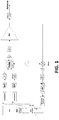
- FIG. 1 is a schematic block diagram showing digital predistortion (DPD) circuits, interpolators, digital-to-analog converters, a modulator, a power amplifier, a duplexer, radio frequency down-conversion circuits for the output coupled at the output of the PA, an analog-to-digital converter for digital predistortion feedback path, and a digital down-converter.
- the digital predistortion system utilizes a delay estimation based on the magnitude of complex signals (I and Q). Normally, the sample rate of the feedback ADC is twice that of the digital pre-distorter.
- sample rate of feedback ADC is typically at least 250 MHz, which means that minimum resolution of the hardware controllable delay is 4 ns (1/250 MHz). In some implementations, this minimum resolution is not small enough to align the delay between transmit and feedback path with desired accuracy in the case of widely frequency spaced carriers.
- the delay estimator receives inputs from the feedback path as well as inputs from the output of the DPD circuit.
- the delay estimator calculates the difference between these inputs and provides inputs to the coefficient estimator in order to time align the signals as part of the error minimization process.
- the delay estimator provides a value, which is a function of the timing error between the in-phase component at the output of the DPD circuit and the in-phase component of the feedback signal and the quadrature-phase component at the output of the DPD circuit and the quadrature-phase component of the feedback signal.
- the function of the timing error which can also be referred to as a function related to the timing error
- the function can be the mean squared error difference between the complex feedback signal and the complex output of the DPD circuit.
- Error I ⁇ ⁇ I 2 + Q ⁇ ⁇ Q 2
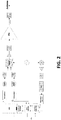
- FIG. 2 is a schematic block diagram showing a system for aligning wideband signals according to an embodiment of the present invention.
- the system illustrated in FIG. 2 includes digital predistortion (DPD) circuits, interpolators, digital-to-analog converters, a modulator, a power amplifier, a duplexer, radio frequency down-conversion circuits for the output coupled at the output of the PA, an analog-to-digital converter for feedback path, a digital down-converter, and a fractional delay filter with controllable parameter (mu) which ranges 0 to 1 in some embodiments.
- DPD digital predistortion
- the fractional delay filter is implemented based on a third order Lagrange Farrow structure that enables a simple implementation and operates at the digital predistortion sample rate.
- a higher order Lagrange Farrow filter can be used as appropriate to the particular application.
- Minimum delay resolution can be 10 times the sample rate or higher, which means that it can be as small as 0.1 ns for a feedback ADC having a sample rate of 1 GHz. Of course, the minimum delay resolution will depend on the number of bits in some implementations. In order to provide a similar minimum delay, conventional systems would use a 10 GHz sample rate interpolator in hardware or complicated and time consuming software filtering algorithm.
- the fractional delay filter allows for shifting of the signal (i.e., time shifting of a signal) by fractions of the sampling rate.
- the fractional delay filter includes a parameter illustrated as mu.
- the parameter enables shifting of the signal to change the delay by a predetermined fraction of the sampling rate, for example, one-tenth of the sampling rate.
- the fractional delay filter enables reduction in minimum delays from 10 ns to 1 ns for a mu value ranging from 0 to 1.
- Embodiments of the present invention thus utilize fractional delay filtering in the context of digital predistortion in wideband communications systems.
- the fractional delay filter serves as a low pass filter with variable delay as a function of the parameter mu. Additional description related to the variation of the parameter mu during operation is provided below.
- FIG 3 is a flow chart illustrating a method of temporally aligning signals according to an embodiment of the present invention.
- the step size can be set to a variety of values, for example, 0.2, 0.1, 0.05, or the like. As an example, if the ADC is operating at a sample rate of 1 MHz (i.e., 1 ⁇ s per sample) and the step size is set to 0.1, then mu will be set to multiples of 0.1 as the counter is incremented in order to provide a minimum delay resolution of 0.1 ⁇ s.
- Signals are captured at the outputs of the DPD circuit and the output of the feedback path (i.e., the outputs of the digital down converter).
- the output of the DPD circuit, and the output of the feedback path are magnitude aligned.
- a calculation of the function of the timing error is performed in the delay estimator as illustrated in FIG. 2 .
- the process iterates until the function of the timing error is less than the predetermined threshold, mu is fixed, and the values from the delay estimator are provided to the coefficient estimator (i.e., the coefficient estimation algorithm).
- the step size is not limited to the value of 0.1 in this example and can be set at other values as appropriate, for example, 0.2, 0.1, 0.05, or the like.
- Embodiments of the present invention provide for adaptive processing in real time to reduce signal error to a predetermined level.
- a predetermined number of symbols are captured (e.g., 4000 samples), a calculation of the function of the timing error is performed to determine the delay estimation value and then the coefficient estimator is provided with the delay.
- a method of temporally aligning signals includes a) computing a value of a delay parameter, b) receiving a plurality of transmit signals, and c) receiving a plurality of feedback signals.
- computing the value of the delay parameter can include multiplying the counter times a step size parameter.
- the step size parameter can range from 0 to 1.
- the method also includes d) determining a function of the timing error using the plurality of transmit signals and the plurality of feedback signals and e) determining that the function of the timing error is greater than or equal to a predetermined threshold. Determining the function of the timing error using the plurality of transmit signals and the plurality of feedback signals can include filtering the plurality of transmit signals and the plurality of feedback signals and estimating the timing error.
- the method further includes f) incrementing a counter and g) repeating a) through f) one or more times. In some embodiments, a subset of a) through f) are repeated one or more times. As illustrated in FIG. 3 , the iteration of a) through f) is performed as long as the function of the timing error is greater than or equal to the predetermined threshold.
- the method After a number of iterations and increases in the value of the delay parameter, the method includes h) determining that the function of the timing error is less than the predetermined threshold and i) fixing the delay parameter. In an embodiment, the method also includes estimating predistortion coefficients using the delay parameter.
- FIG. 3 provides a particular method of temporally aligning signals according to an embodiment of the present invention. Other sequences of steps may also be performed according to alternative embodiments. For example, alternative embodiments of the present invention may perform the steps outlined above in a different order. Moreover, the individual steps illustrated in FIG. 3 may include multiple sub-steps that may be performed in various sequences as appropriate to the individual step. Furthermore, additional steps may be added or removed depending on the particular applications.
- One of ordinary skill in the art would recognize many variations, modifications, and alternatives.
Landscapes
- Engineering & Computer Science (AREA)
- Power Engineering (AREA)
- Physics & Mathematics (AREA)
- Computer Networks & Wireless Communication (AREA)
- Signal Processing (AREA)
- Nonlinear Science (AREA)
- General Physics & Mathematics (AREA)
- Mathematical Analysis (AREA)
- Mathematical Optimization (AREA)
- Pure & Applied Mathematics (AREA)
- Algebra (AREA)
- Amplifiers (AREA)
- Transmitters (AREA)
Applications Claiming Priority (3)
| Application Number | Priority Date | Filing Date | Title |
|---|---|---|---|
| US201261674771P | 2012-07-23 | 2012-07-23 | |
| EP13823723.5A EP2875620B1 (en) | 2012-07-23 | 2013-07-18 | Method and system for aligning signals widely spaced in frequency for wideband digital predistortion in wireless communication systems |
| PCT/US2013/051149 WO2014018379A1 (en) | 2012-07-23 | 2013-07-18 | Method and system for aligning signals widely spaced in frequency for wideband digital predistortion in wireless communication systems |
Related Parent Applications (2)
| Application Number | Title | Priority Date | Filing Date |
|---|---|---|---|
| EP13823723.5A Division-Into EP2875620B1 (en) | 2012-07-23 | 2013-07-18 | Method and system for aligning signals widely spaced in frequency for wideband digital predistortion in wireless communication systems |
| EP13823723.5A Division EP2875620B1 (en) | 2012-07-23 | 2013-07-18 | Method and system for aligning signals widely spaced in frequency for wideband digital predistortion in wireless communication systems |
Publications (1)
| Publication Number | Publication Date |
|---|---|
| EP3745664A1 true EP3745664A1 (en) | 2020-12-02 |
Family
ID=49997743
Family Applications (2)
| Application Number | Title | Priority Date | Filing Date |
|---|---|---|---|
| EP13823723.5A Active EP2875620B1 (en) | 2012-07-23 | 2013-07-18 | Method and system for aligning signals widely spaced in frequency for wideband digital predistortion in wireless communication systems |
| EP20186758.7A Withdrawn EP3745664A1 (en) | 2012-07-23 | 2013-07-18 | Method and system for aligning signals widely spaced in frequency for wideband digital predistortion in wireless communication systems |
Family Applications Before (1)
| Application Number | Title | Priority Date | Filing Date |
|---|---|---|---|
| EP13823723.5A Active EP2875620B1 (en) | 2012-07-23 | 2013-07-18 | Method and system for aligning signals widely spaced in frequency for wideband digital predistortion in wireless communication systems |
Country Status (9)
| Country | Link |
|---|---|
| US (3) | US9225296B2 (zh) |
| EP (2) | EP2875620B1 (zh) |
| JP (2) | JP6542120B2 (zh) |
| KR (1) | KR102141257B1 (zh) |
| CN (1) | CN104584501B (zh) |
| BR (1) | BR112015001348B1 (zh) |
| HK (1) | HK1208291A1 (zh) |
| IL (2) | IL236619B (zh) |
| WO (1) | WO2014018379A1 (zh) |
Families Citing this family (15)
| Publication number | Priority date | Publication date | Assignee | Title |
|---|---|---|---|---|
| AU2012302074B2 (en) | 2011-08-29 | 2017-02-16 | Commscope Technologies Llc | Configuring a distributed antenna system |
| JP6542120B2 (ja) | 2012-07-23 | 2019-07-10 | ダリ システムズ カンパニー リミテッド | ワイヤレス通信システムにおける広帯域デジタルプリディストーションのために周波数が広く離間している信号を整合させるための方法及びシステム |
| US9306507B2 (en) * | 2013-07-12 | 2016-04-05 | Intel Deutschland Gmbh | Controller and method for controlling a signal processor |
| US20150092825A1 (en) * | 2013-09-27 | 2015-04-02 | Qualcomm Incorporated | Self-test using internal feedback for transmit signal quality estimation |
| EP3230800B1 (en) | 2015-03-06 | 2021-02-17 | HP Indigo B.V. | Image transfer for liquid electro-photographic printing |
| US9712343B2 (en) | 2015-06-19 | 2017-07-18 | Andrew Wireless Systems Gmbh | Scalable telecommunications system |
| US10079702B2 (en) * | 2015-07-06 | 2018-09-18 | Mediatek Singapore Pte. Ltd. | Front-end module and coupling compensation for closed-loop digital pre-distortion system |
| CN105516051A (zh) * | 2015-11-26 | 2016-04-20 | 西安电子科技大学 | 数字预失真分数时延估计与信号对齐算法及系统 |
| EP3264598B1 (en) * | 2016-07-01 | 2019-10-09 | Nokia Solutions and Networks Oy | Improved feedback in miso systems |
| US10003310B1 (en) * | 2016-12-07 | 2018-06-19 | Nxp Usa, Inc. | Segmented digital predistortion apparatus and methods |
| TWI700888B (zh) * | 2019-08-30 | 2020-08-01 | 中磊電子股份有限公司 | 數位預失真電路及數位預失真方法 |
| US10887079B1 (en) * | 2019-09-26 | 2021-01-05 | Corning Research & Development Corporation | Digital predistortion (DPD) timing alignment in a remote unit(s) for a wireless communications system (WCS) |
| KR20220118990A (ko) * | 2019-12-23 | 2022-08-26 | 주식회사 아도반테스토 | 입력 샘플 세트를 기반으로 복수의 출력 샘플을 제공하는 신호 처리 장치 및 입력 샘플 세트를 기반으로 복수의 출력 샘플을 제공하는 방법 |
| US11329687B2 (en) * | 2020-01-20 | 2022-05-10 | Texas Instruments Incorporated | Transceiver circuit with digital pre-distortion (DPD) options |
| US11190230B1 (en) | 2020-05-29 | 2021-11-30 | Corning Research & Development Corporation | Wide bandwidth digital pre-distortion (DPD) in a remote unit(s) for a wireless communications system (WCS) |
Citations (4)
| Publication number | Priority date | Publication date | Assignee | Title |
|---|---|---|---|---|
| WO2002017586A1 (en) * | 2000-08-18 | 2002-02-28 | Nokia Corporation | Multicarrier transmitter circuit arrangement with predistortion linearisation method |
| US7602244B1 (en) * | 2007-11-27 | 2009-10-13 | Nortel Networks Limited | Power amplifier bias synchronization |
| US20110156815A1 (en) * | 2009-12-21 | 2011-06-30 | Dali Systems Co., Ltd. | Modulation agnostic digital hybrid mode power amplifier system and method |
| US20110274210A1 (en) * | 2010-05-04 | 2011-11-10 | Samsung Electronics Co. Ltd. | Time alignment algorithm for transmitters with eer/et amplifiers and others |
Family Cites Families (15)
| Publication number | Priority date | Publication date | Assignee | Title |
|---|---|---|---|---|
| FI105506B (fi) | 1998-04-30 | 2000-08-31 | Nokia Networks Oy | Vahvistimen linearisointimenetelmä ja vahvistinjärjestely |
| US6798843B1 (en) | 1999-07-13 | 2004-09-28 | Pmc-Sierra, Inc. | Wideband digital predistortion linearizer for nonlinear amplifiers |
| JP4014343B2 (ja) | 1999-12-28 | 2007-11-28 | 富士通株式会社 | 歪補償装置 |
| SE0102885D0 (en) | 2001-08-28 | 2001-08-28 | Ericsson Telefon Ab L M | Calibration of an adaptive signal conditioning systern |
| FR2835120B1 (fr) | 2002-01-21 | 2006-10-20 | Evolium Sas | Procede et dispositif de preparation de signaux destines a etre compares pour etablir une pre-distorsion sur l'entree d'un amplificateur |
| SE0301273D0 (sv) | 2003-04-30 | 2003-04-30 | Coding Technologies Sweden Ab | Advanced processing based on a complex-exponential-modulated filterbank and adaptive time signalling methods |
| US7577211B2 (en) * | 2004-03-01 | 2009-08-18 | Powerwave Technologies, Inc. | Digital predistortion system and method for linearizing an RF power amplifier with nonlinear gain characteristics and memory effects |
| CN101228690B (zh) | 2005-07-29 | 2010-08-18 | 富士通株式会社 | 延迟调整装置 |
| JP4863729B2 (ja) | 2006-02-14 | 2012-01-25 | 富士通株式会社 | 歪補償装置及び歪補償方法 |
| JP5104623B2 (ja) | 2008-07-29 | 2012-12-19 | 富士通株式会社 | 遅延量推定装置および信号送信装置 |
| JP5146404B2 (ja) * | 2009-05-21 | 2013-02-20 | 富士通株式会社 | 歪補償装置 |
| JP5158034B2 (ja) * | 2009-08-12 | 2013-03-06 | 富士通株式会社 | 無線装置及び信号処理方法 |
| JP5303809B2 (ja) * | 2009-10-20 | 2013-10-02 | 株式会社日立国際電気 | 歪補償装置 |
| JP6542120B2 (ja) | 2012-07-23 | 2019-07-10 | ダリ システムズ カンパニー リミテッド | ワイヤレス通信システムにおける広帯域デジタルプリディストーションのために周波数が広く離間している信号を整合させるための方法及びシステム |
| US9365751B2 (en) | 2012-07-24 | 2016-06-14 | Henkel IP & Holding GmbH | Reactive hot melt adhesive |
-
2013
- 2013-07-18 JP JP2015524332A patent/JP6542120B2/ja active Active
- 2013-07-18 EP EP13823723.5A patent/EP2875620B1/en active Active
- 2013-07-18 US US13/945,736 patent/US9225296B2/en active Active
- 2013-07-18 CN CN201380039353.6A patent/CN104584501B/zh active Active
- 2013-07-18 WO PCT/US2013/051149 patent/WO2014018379A1/en active Application Filing
- 2013-07-18 EP EP20186758.7A patent/EP3745664A1/en not_active Withdrawn
- 2013-07-18 BR BR112015001348-1A patent/BR112015001348B1/pt active IP Right Grant
- 2013-07-18 KR KR1020157004064A patent/KR102141257B1/ko active IP Right Grant
-
2015
- 2015-01-11 IL IL236619A patent/IL236619B/en active IP Right Grant
- 2015-09-10 HK HK15108803.3A patent/HK1208291A1/zh unknown
- 2015-12-01 US US14/956,040 patent/US10263569B2/en active Active
-
2018
- 2018-05-17 IL IL259447A patent/IL259447A/en unknown
-
2019
- 2019-03-13 US US16/352,065 patent/US11394350B2/en active Active
- 2019-06-12 JP JP2019109166A patent/JP2019180093A/ja active Pending
Patent Citations (4)
| Publication number | Priority date | Publication date | Assignee | Title |
|---|---|---|---|---|
| WO2002017586A1 (en) * | 2000-08-18 | 2002-02-28 | Nokia Corporation | Multicarrier transmitter circuit arrangement with predistortion linearisation method |
| US7602244B1 (en) * | 2007-11-27 | 2009-10-13 | Nortel Networks Limited | Power amplifier bias synchronization |
| US20110156815A1 (en) * | 2009-12-21 | 2011-06-30 | Dali Systems Co., Ltd. | Modulation agnostic digital hybrid mode power amplifier system and method |
| US20110274210A1 (en) * | 2010-05-04 | 2011-11-10 | Samsung Electronics Co. Ltd. | Time alignment algorithm for transmitters with eer/et amplifiers and others |
Also Published As
| Publication number | Publication date |
|---|---|
| CN104584501B (zh) | 2019-07-12 |
| IL236619B (en) | 2018-08-30 |
| IL259447A (en) | 2018-07-31 |
| US20200052659A1 (en) | 2020-02-13 |
| EP2875620A1 (en) | 2015-05-27 |
| JP6542120B2 (ja) | 2019-07-10 |
| BR112015001348A2 (pt) | 2017-07-04 |
| IL236619A0 (en) | 2015-02-26 |
| EP2875620B1 (en) | 2020-09-02 |
| JP2019180093A (ja) | 2019-10-17 |
| KR20150034787A (ko) | 2015-04-03 |
| HK1208291A1 (zh) | 2016-02-26 |
| KR102141257B1 (ko) | 2020-08-05 |
| EP2875620A4 (en) | 2016-03-02 |
| WO2014018379A1 (en) | 2014-01-30 |
| US11394350B2 (en) | 2022-07-19 |
| BR112015001348B1 (pt) | 2021-12-21 |
| US20160344351A1 (en) | 2016-11-24 |
| US9225296B2 (en) | 2015-12-29 |
| US20140159810A1 (en) | 2014-06-12 |
| US10263569B2 (en) | 2019-04-16 |
| CN104584501A (zh) | 2015-04-29 |
| JP2015525036A (ja) | 2015-08-27 |
Similar Documents
| Publication | Publication Date | Title |
|---|---|---|
| US11394350B2 (en) | Method and system for aligning signals widely spaced in frequency for wideband digital predistortion in wireless communication systems | |
| US11129076B2 (en) | Method and system for baseband predistortion linearization in multi-channel wideband communication systems | |
| US10749553B2 (en) | System and method for increasing bandwidth for digital predistortion in multi-channel wideband communication systems | |
| US20220368360A1 (en) | Predistortion Circuit, Method For Generating A Predistorted Baseband Signal, Control Circuit For A Predistortion Circuit, Method To Determine Parameters For A Predistortion Circuit, And Apparatus And Method For Predistorting A Baseband Signal | |
| US7606322B2 (en) | Digital pre-distortion technique using nonlinear filters | |
| KR101077349B1 (ko) | 적응형 부대역 전치왜곡기를 사용한 rf 전력 증폭기의 선형화 | |
| CN102075469B (zh) | 用于数字预失真系统的信号延迟时间的估计方法 | |
| US20150091643A1 (en) | Using Fractional Delay Computations to Improve Intermodulation Performance | |
| US8437424B2 (en) | Robust transmit/feedback alignment | |
| JP5141694B2 (ja) | 非線形歪み補償付き増幅装置 | |
| CN201947373U (zh) | 一种高效率数字电视发射装置 | |
| KR101470817B1 (ko) | 복수의 비선형 증폭기에 대하여 단일 피드백 회로를 사용하는 전치보상 장치 및 방법 | |
| Yadav et al. | Linearity improvement of microwave power amplifiers | |
| Varahram et al. | A Low Complexity NARX Structure using Indirect Learning Architecture for Digital Pre-Distortion |
Legal Events
| Date | Code | Title | Description |
|---|---|---|---|
| PUAI | Public reference made under article 153(3) epc to a published international application that has entered the european phase |
Free format text: ORIGINAL CODE: 0009012 |
|
| STAA | Information on the status of an ep patent application or granted ep patent |
Free format text: STATUS: THE APPLICATION HAS BEEN PUBLISHED |
|
| AC | Divisional application: reference to earlier application |
Ref document number: 2875620 Country of ref document: EP Kind code of ref document: P |
|
| AK | Designated contracting states |
Kind code of ref document: A1 Designated state(s): AL AT BE BG CH CY CZ DE DK EE ES FI FR GB GR HR HU IE IS IT LI LT LU LV MC MK MT NL NO PL PT RO RS SE SI SK SM TR |
|
| AX | Request for extension of the european patent |
Extension state: BA ME |
|
| REG | Reference to a national code |
Ref country code: HK Ref legal event code: DE Ref document number: 40032474 Country of ref document: HK |
|
| STAA | Information on the status of an ep patent application or granted ep patent |
Free format text: STATUS: REQUEST FOR EXAMINATION WAS MADE |
|
| 17P | Request for examination filed |
Effective date: 20210525 |
|
| RBV | Designated contracting states (corrected) |
Designated state(s): AL AT BE BG CH CY CZ DE DK EE ES FI FR GB GR HR HU IE IS IT LI LT LU LV MC MK MT NL NO PL PT RO RS SE SI SK SM TR |
|
| STAA | Information on the status of an ep patent application or granted ep patent |
Free format text: STATUS: EXAMINATION IS IN PROGRESS |
|
| P01 | Opt-out of the competence of the unified patent court (upc) registered |
Effective date: 20230424 |
|
| 17Q | First examination report despatched |
Effective date: 20230523 |
|
| STAA | Information on the status of an ep patent application or granted ep patent |
Free format text: STATUS: THE APPLICATION IS DEEMED TO BE WITHDRAWN |
|
| 18D | Application deemed to be withdrawn |
Effective date: 20231205 |