EP2875620B1 - Method and system for aligning signals widely spaced in frequency for wideband digital predistortion in wireless communication systems - Google Patents
Method and system for aligning signals widely spaced in frequency for wideband digital predistortion in wireless communication systems Download PDFInfo
- Publication number
- EP2875620B1 EP2875620B1 EP13823723.5A EP13823723A EP2875620B1 EP 2875620 B1 EP2875620 B1 EP 2875620B1 EP 13823723 A EP13823723 A EP 13823723A EP 2875620 B1 EP2875620 B1 EP 2875620B1
- Authority
- EP
- European Patent Office
- Prior art keywords
- delay
- function
- signals
- timing error
- feedback
- Prior art date
- Legal status (The legal status is an assumption and is not a legal conclusion. Google has not performed a legal analysis and makes no representation as to the accuracy of the status listed.)
- Active
Links
- 238000000034 method Methods 0.000 title claims description 44
- 238000004891 communication Methods 0.000 title description 6
- 230000003044 adaptive effect Effects 0.000 claims description 7
- 238000005070 sampling Methods 0.000 claims description 7
- 238000001914 filtration Methods 0.000 claims description 4
- 238000005314 correlation function Methods 0.000 claims 1
- 238000010586 diagram Methods 0.000 description 4
- 230000008901 benefit Effects 0.000 description 3
- 238000006243 chemical reaction Methods 0.000 description 3
- 230000003750 conditioning effect Effects 0.000 description 3
- 238000013461 design Methods 0.000 description 3
- 230000006978 adaptation Effects 0.000 description 2
- 238000004364 calculation method Methods 0.000 description 2
- 239000000969 carrier Substances 0.000 description 2
- 238000005516 engineering process Methods 0.000 description 2
- 230000008569 process Effects 0.000 description 2
- 238000012545 processing Methods 0.000 description 2
- 230000003595 spectral effect Effects 0.000 description 2
- 230000008859 change Effects 0.000 description 1
- 239000002131 composite material Substances 0.000 description 1
- 238000007796 conventional method Methods 0.000 description 1
- 230000001934 delay Effects 0.000 description 1
- 230000003111 delayed effect Effects 0.000 description 1
- 230000000694 effects Effects 0.000 description 1
- 238000010295 mobile communication Methods 0.000 description 1
- 238000012986 modification Methods 0.000 description 1
- 230000004048 modification Effects 0.000 description 1
- 230000009467 reduction Effects 0.000 description 1
- 238000000926 separation method Methods 0.000 description 1
Images
Classifications
-
- H—ELECTRICITY
- H03—ELECTRONIC CIRCUITRY
- H03F—AMPLIFIERS
- H03F1/00—Details of amplifiers with only discharge tubes, only semiconductor devices or only unspecified devices as amplifying elements
- H03F1/32—Modifications of amplifiers to reduce non-linear distortion
- H03F1/3241—Modifications of amplifiers to reduce non-linear distortion using predistortion circuits
- H03F1/3247—Modifications of amplifiers to reduce non-linear distortion using predistortion circuits using feedback acting on predistortion circuits
-
- H—ELECTRICITY
- H03—ELECTRONIC CIRCUITRY
- H03F—AMPLIFIERS
- H03F1/00—Details of amplifiers with only discharge tubes, only semiconductor devices or only unspecified devices as amplifying elements
- H03F1/32—Modifications of amplifiers to reduce non-linear distortion
- H03F1/3241—Modifications of amplifiers to reduce non-linear distortion using predistortion circuits
- H03F1/3258—Modifications of amplifiers to reduce non-linear distortion using predistortion circuits based on polynomial terms
-
- H—ELECTRICITY
- H03—ELECTRONIC CIRCUITRY
- H03F—AMPLIFIERS
- H03F3/00—Amplifiers with only discharge tubes or only semiconductor devices as amplifying elements
- H03F3/189—High frequency amplifiers, e.g. radio frequency amplifiers
-
- H—ELECTRICITY
- H03—ELECTRONIC CIRCUITRY
- H03F—AMPLIFIERS
- H03F3/00—Amplifiers with only discharge tubes or only semiconductor devices as amplifying elements
- H03F3/20—Power amplifiers, e.g. Class B amplifiers, Class C amplifiers
- H03F3/24—Power amplifiers, e.g. Class B amplifiers, Class C amplifiers of transmitter output stages
- H03F3/245—Power amplifiers, e.g. Class B amplifiers, Class C amplifiers of transmitter output stages with semiconductor devices only
-
- H—ELECTRICITY
- H04—ELECTRIC COMMUNICATION TECHNIQUE
- H04L—TRANSMISSION OF DIGITAL INFORMATION, e.g. TELEGRAPHIC COMMUNICATION
- H04L25/00—Baseband systems
- H04L25/02—Details ; arrangements for supplying electrical power along data transmission lines
- H04L25/03—Shaping networks in transmitter or receiver, e.g. adaptive shaping networks
- H04L25/03006—Arrangements for removing intersymbol interference
- H04L25/03012—Arrangements for removing intersymbol interference operating in the time domain
- H04L25/03019—Arrangements for removing intersymbol interference operating in the time domain adaptive, i.e. capable of adjustment during data reception
- H04L25/03057—Arrangements for removing intersymbol interference operating in the time domain adaptive, i.e. capable of adjustment during data reception with a recursive structure
- H04L25/03063—Arrangements for removing intersymbol interference operating in the time domain adaptive, i.e. capable of adjustment during data reception with a recursive structure using fractionally spaced delay lines or combinations of fractionally and integrally spaced taps
-
- H—ELECTRICITY
- H04—ELECTRIC COMMUNICATION TECHNIQUE
- H04L—TRANSMISSION OF DIGITAL INFORMATION, e.g. TELEGRAPHIC COMMUNICATION
- H04L25/00—Baseband systems
- H04L25/02—Details ; arrangements for supplying electrical power along data transmission lines
- H04L25/03—Shaping networks in transmitter or receiver, e.g. adaptive shaping networks
- H04L25/03006—Arrangements for removing intersymbol interference
- H04L25/03343—Arrangements at the transmitter end
-
- H—ELECTRICITY
- H04—ELECTRIC COMMUNICATION TECHNIQUE
- H04L—TRANSMISSION OF DIGITAL INFORMATION, e.g. TELEGRAPHIC COMMUNICATION
- H04L43/00—Arrangements for monitoring or testing data switching networks
- H04L43/02—Capturing of monitoring data
- H04L43/028—Capturing of monitoring data by filtering
-
- H—ELECTRICITY
- H03—ELECTRONIC CIRCUITRY
- H03F—AMPLIFIERS
- H03F2200/00—Indexing scheme relating to amplifiers
- H03F2200/336—A I/Q, i.e. phase quadrature, modulator or demodulator being used in an amplifying circuit
-
- H—ELECTRICITY
- H03—ELECTRONIC CIRCUITRY
- H03F—AMPLIFIERS
- H03F2200/00—Indexing scheme relating to amplifiers
- H03F2200/451—Indexing scheme relating to amplifiers the amplifier being a radio frequency amplifier
-
- H—ELECTRICITY
- H04—ELECTRIC COMMUNICATION TECHNIQUE
- H04L—TRANSMISSION OF DIGITAL INFORMATION, e.g. TELEGRAPHIC COMMUNICATION
- H04L27/00—Modulated-carrier systems
- H04L27/0002—Modulated-carrier systems analog front ends; means for connecting modulators, demodulators or transceivers to a transmission line
-
- H—ELECTRICITY
- H04—ELECTRIC COMMUNICATION TECHNIQUE
- H04L—TRANSMISSION OF DIGITAL INFORMATION, e.g. TELEGRAPHIC COMMUNICATION
- H04L27/00—Modulated-carrier systems
- H04L27/26—Systems using multi-frequency codes
- H04L27/2601—Multicarrier modulation systems
- H04L27/2626—Arrangements specific to the transmitter only
- H04L27/2627—Modulators
-
- H—ELECTRICITY
- H04—ELECTRIC COMMUNICATION TECHNIQUE
- H04L—TRANSMISSION OF DIGITAL INFORMATION, e.g. TELEGRAPHIC COMMUNICATION
- H04L27/00—Modulated-carrier systems
- H04L27/26—Systems using multi-frequency codes
- H04L27/2601—Multicarrier modulation systems
- H04L27/2647—Arrangements specific to the receiver only
- H04L27/2655—Synchronisation arrangements
Definitions
- Predistortion is a technique used in communciations systems to improve the linearity of power amplifiers. Because power amplifiers can have nonlinear input/output characteristics, predistortion is used to linearize the input/output characteristics of the power amplifier. In essence, "inverse distortion" is introduced into the input fed to the power amplifier, thereby cancelling the non-linear characteristics of the power amplifier.
- DSP digital signal processing
- the analog predistorter is based on the principle of error subtraction and power matching to produce linearization of the power amplifier. Because nonlinear characteristics of power amplifiers can be complicated and involve many variables, analog predistortion results in less than optimal predistortion accuracy and consumes significant power.
- Document WO 02/17586 A1 discloses a multicarrier circuit arrangement and a method for linearising same in which frequency channels are combined using a complex mixing operation to generate a single composite complex signal, so as to achieve a complex channel separation. A predistorted complex signal is then generated by applying a complex predistortion to said complex signal.
- Document US 7,602,244 B1 discloses a power amplifier system including a non-linear power amplifier that receives a predistorted input signal.
- a receive receives an output signal from the power amplifier and provides an observed signal.
- a bias controller provides a delayed dynamic bias signal to the power amplifier wherein the bias signal delay is dynamic and is a function of the observed signal for synchronizing the predistorted input signal with the dynamic bias signal.
- Document US 2011/0156815 A1 discloses an RF-digital hybrid mode power amplifier system for wideband communication systems. The disclosed method is based on adaptive signal predistortion to linearize a power amplifier in the RF domain.
- Document WO 03/019773 A1 discloses an adaptive signal conditioning system having a signal conditioning block in the signal path to a signal conversion system, and a feedback path with a number of feedback components for enabling adaptation, by means of a parameter adaptation block, of the parameters used in the signal conditioning.
- the present invention has been made in view of the above problems, and it is an object of the present invention to provide a robust method of estimating delay between the transmit and feedback signals for a wideband digital predistortion system.
- the technique is based on using a Farrow based fractional delay filter in the feedback path and an algorithm in order to accurately control the feedback path delay.
- Embodiments of the present invention are able to time align transmit and feedback signals with high accuracy at any time.
- a simple and robust delay estimation method for wideband digital predistortion with widely frequency spaced carriers is provided.
- the present invention provides a method of time aligning a transmit and feedback signal, for a wideband digital predistortion system.
- the technique is based on using a programmable fractional delay filter based on a third order Lagrange Farrow structure which is very simple to design and control.
- Embodiments described herein are able to align signals, in digital predistortion systems, with more than an instantaneous 100 MHz bandwidth.
- a system for time aligning widely frequency spaced signals includes a digital predistortion (DPD) processor and a power amplifier coupled to the DPD processor and operable to provide a transmit signal at a power amplifier output.
- the system also includes a feedback loop coupled to the power amplifier output.
- the feedback loop includes an adaptive fractional delay filter, a delay estimator coupled to the adaptive fractional delay filter, and a DPD coefficient estimator coupled to the delay estimator, as defined in claim 1.
- a method of temporally aligning signals includes a) computing a value of a delay parameter, b) receiving a plurality of transmit signals, and c) receiving a plurality of feedback signals.
- the method also includes d) determining a function related to a timing error using the plurality of transmit signals and the plurality of feedback signals, e) determining that the function related to the timing error is greater than or equal to a predetermined threshold, and f) incrementing a counter.
- the method further includes g) repeating one or more of a) through f) one or more times, h) determining that the function related to the timing error is less than the predetermined threshold, and i) fixing the delay parameter, as defined in claim 4.
- embodiments of the present invention provide for enhanced control of delay in the feedback path, improving the performance characteristics of the digital predistortion system.
- the present invention generally relates to wideband communication systems using multiplexing modulation techniques. More specially, the present invention relates to a method of aligning widely frequency spaced signals for wideband digital predistortion linearization in wireless transmitters.
- RF PAs radio frequency
- PAs radio frequency
- PARs peak to average power ratio
- RF PAs have nonlinearities which generate amplitude modulation - amplitude modulation (AM-AM) and amplitude modulation - phase modulation (AM-PM) distortion at the output of the PA.
- AM-AM amplitude modulation - amplitude modulation
- AM-PM amplitude modulation - phase modulation
- EVM error vector magnitude
- DPD baseband digital predistortion
- DPA Doherty power amplifier
- the typical wireless communication systems instantaneous bandwidth supports around 20 MHz to 25 MHz.
- the common delay estimation for digital predistortion algorithm uses magnitude correlation between the transmit signal and feedback signal with two times or more oversampling.
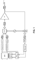
- FIG. 1 is a schematic block diagram showing digital predistortion (DPD) circuits, interpolators, digital-to-analog converters, a modulator, a power amplifier, a duplexer, radio frequency down-conversion circuits for the output coupled at the output of the PA, an analog-to-digital converter for digital predistortion feedback path, and a digital down-converter.
- the digital predistortion system utilizes a delay estimation based on the magnitude of complex signals (I and Q). Normally, the sample rate of the feedback ADC is twice that of the digital pre-distorter.
- sample rate of feedback ADC is typically at least 250 MHz, which means that minimum resolution of the hardware controllable delay is 4 ns (1/250 MHz). In some implementations, this minimum resolution is not small enough to align the delay between transmit and feedback path with desired accuracy in the case of widely frequency spaced carriers.
- the delay estimator receives inputs from the feedback path as well as inputs from the output of the DPD circuit.
- the delay estimator calculates the difference between these inputs and provides inputs to the coefficient estimator in order to time align the signals as part of the error minimization process.
- the delay estimator provides a value, which is a function of the timing error between the inphase component at the output of the DPD circuit and the in-phase component of the feedback signal and the quadrature-phase component at the output of the DPD circuit and the quadrature-phase component of the feedback signal.
- the function of the timing error which can also be referred to as a function related to the timing error
- the function can be the mean squared error difference between the complex feedback signal and the complex output of the DPD circuit.
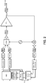
- FIG. 2 is a schematic block diagram showing a system for aligning wideband signals according to an embodiment of the present invention.
- the system illustrated in FIG. 2 includes digital predistortion (DPD) circuits, interpolators, digital-to-analog converters, a modulator, a power amplifier, a duplexer, radio frequency down-conversion circuits for the output coupled at the output of the PA, an analog-to-digital converter for feedback path, a digital down-converter, and a fractional delay filter with controllable parameter (mu) which ranges 0 to 1 in some embodiments.
- DPD digital predistortion
- the fractional delay filter is implemented based on a third order Lagrange Farrow structure that enables a simple implementation and operates at the digital predistortion sample rate.
- a higher order Lagrange Farrow filter can be used as appropriate to the particular application.
- Minimum delay resolution can be 10 times the sample rate or higher, which means that it can be as small as 0.1 ns for a feedback ADC having a sample rate of 1 GHz. Of course, the minimum delay resolution will depend on the number of bits in some implementations. In order to provide a similar minimum delay, conventional systems would use a 10 GHz sample rate interpolator in hardware or complicated and time consuming software filtering algorithm.
- the fractional delay filter allows for shifting of the signal (i.e., time shifting of a signal) by fractions of the sampling rate.
- the fractional delay filter includes a parameter illustrated as mu.
- the parameter enables shifting of the signal to change the delay by a predetermined fraction of the sampling rate, for example, one-tenth of the sampling rate.
- the fractional delay filter enables reduction in minimum delays from 10 ns to 1 ns for a mu value ranging from 0 to 1.
- Embodiments of the present invention thus utilize fractional delay filtering in the context of digital predistortion in wideband communications systems.
- the fractional delay filter serves as a low pass filter with variable delay as a function of the parameter mu. Additional description related to the variation of the parameter mu during operation is provided below.
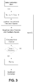
- FIG 3 is a flow chart illustrating a method of temporally aligning signals according to an embodiment of the present invention.
- the step size can be set to a variety of values, for example, 0.2, 0.1, 0.05, or the like. As an example, if the ADC is operating at a sample rate of 1 MHz (i.e., 1 ⁇ s per sample) and the step size is set to 0.1, then mu will be set to multiples of 0.1 as the counter is incremented in order to provide a minimum delay resolution of 0.1 ⁇ s.
- Signals are captured at the outputs of the DPD circuit and the output of the feedback path (i.e., the outputs of the digital down converter).
- the output of the DPD circuit, and the output of the feedback path are magnitude aligned.
- a calculation of the function of the timing error is performed in the delay estimator as illustrated in FIG. 2 .
- the process iterates until the function of the timing error is less than the predetermined threshold, mu is fixed, and the values from the delay estimator are provided to the coefficient estimator (i.e., the coefficient estimation algorithm).
- the step size is not limited to the value of 0.1 in this example and can be set at other values as appropriate, for example, 0.2, 0.1, 0.05, or the like.
- Embodiments of the present invention provide for adaptive processing in real time to reduce signal error to a predetermined level.
- a predetermined number of symbols are captured (e.g., 4000 samples), a calculation of the function of the timing error is performed to determine the delay estimation value and then the coefficient estimator is provided with the delay.
- a method of temporally aligning signals includes a) computing a value of a delay parameter, b) receiving a plurality of transmit signals, and c) receiving a plurality of feedback signals.
- computing the value of the delay parameter can include multiplying the counter times a step size parameter.
- the step size parameter can range from 0 to 1.
- the method also includes d) determining a function of the timing error using the plurality of transmit signals and the plurality of feedback signals and e) determining that the function of the timing error is greater than or equal to a predetermined threshold. Determining the function of the timing error using the plurality of transmit signals and the plurality of feedback signals can include filtering the plurality of transmit signals and the plurality of feedback signals and estimating the timing error.
- the method further includes f) incrementing a counter and g) repeating a) through f) one or more times. In some embodiments, a subset of a) through f) are repeated one or more times. As illustrated in FIG. 3 , the iteration of a) through f) is performed as long as the function of the timing error is greater than or equal to the predetermined threshold.
- the method After a number of iterations and increases in the value of the delay parameter, the method includes h) determining that the function of the timing error is less than the predetermined threshold and i) fixing the delay parameter. In an embodiment, the method also includes estimating predistortion coefficients using the delay parameter.
- FIG. 3 provides a particular method of temporally aligning signals according to an embodiment of the present invention. Other sequences of steps may also be performed according to alternative embodiments. For example, alternative embodiments of the present invention may perform the steps outlined above in a different order. Moreover, the individual steps illustrated in FIG. 3 may include multiple sub-steps that may be performed in various sequences as appropriate to the individual step. Furthermore, additional steps may be added depending on the particular applications.
Description
- Predistortion is a technique used in communciations systems to improve the linearity of power amplifiers. Because power amplifiers can have nonlinear input/output characteristics, predistortion is used to linearize the input/output characteristics of the power amplifier. In essence, "inverse distortion" is introduced into the input fed to the power amplifier, thereby cancelling the non-linear characteristics of the power amplifier.
- Current predistortion technologies used to linearize power amplifiers in mobile communication systems are mainly analog predistorters implemented at IF/RF by means of analog circuitry and a digital predistorter at baseband with digital signal processing (DSP) techniques.
- The analog predistorter is based on the principle of error subtraction and power matching to produce linearization of the power amplifier. Because nonlinear characteristics of power amplifiers can be complicated and involve many variables, analog predistortion results in less than optimal predistortion accuracy and consumes significant power.
- Despite the progress made in predistortion technologies, there is a need in the art for improved methods and systems for digital predistortion systems.
- Document
WO 02/17586 A1 - Document
US 7,602,244 B1 discloses a power amplifier system including a non-linear power amplifier that receives a predistorted input signal. A receive receives an output signal from the power amplifier and provides an observed signal. A bias controller provides a delayed dynamic bias signal to the power amplifier wherein the bias signal delay is dynamic and is a function of the observed signal for synchronizing the predistorted input signal with the dynamic bias signal. - Document
US 2011/0156815 A1 discloses an RF-digital hybrid mode power amplifier system for wideband communication systems. The disclosed method is based on adaptive signal predistortion to linearize a power amplifier in the RF domain. - Document
WO 03/019773 A1 - Accordingly, the present invention has been made in view of the above problems, and it is an object of the present invention to provide a robust method of estimating delay between the transmit and feedback signals for a wideband digital predistortion system. To achieve the above objective, the technique is based on using a Farrow based fractional delay filter in the feedback path and an algorithm in order to accurately control the feedback path delay. Embodiments of the present invention are able to time align transmit and feedback signals with high accuracy at any time.
- A simple and robust delay estimation method for wideband digital predistortion with widely frequency spaced carriers is provided. The present invention provides a method of time aligning a transmit and feedback signal, for a wideband digital predistortion system. To achieve the above objective, according to an embodiment of the present invention, the technique is based on using a programmable fractional delay filter based on a third order Lagrange Farrow structure which is very simple to design and control. Embodiments described herein are able to align signals, in digital predistortion systems, with more than an instantaneous 100 MHz bandwidth.
- According to an aspect of the present invention, a system for time aligning widely frequency spaced signals is provided. The system includes a digital predistortion (DPD) processor and a power amplifier coupled to the DPD processor and operable to provide a transmit signal at a power amplifier output. The system also includes a feedback loop coupled to the power amplifier output. The feedback loop includes an adaptive fractional delay filter, a delay estimator coupled to the adaptive fractional delay filter, and a DPD coefficient estimator coupled to the delay estimator, as defined in
claim 1. - According to another aspect of the present invention, a method of temporally aligning signals is provided. The method includes a) computing a value of a delay parameter, b) receiving a plurality of transmit signals, and c) receiving a plurality of feedback signals. The method also includes d) determining a function related to a timing error using the plurality of transmit signals and the plurality of feedback signals, e) determining that the function related to the timing error is greater than or equal to a predetermined threshold, and f) incrementing a counter. The method further includes g) repeating one or more of a) through f) one or more times, h) determining that the function related to the timing error is less than the predetermined threshold, and i) fixing the delay parameter, as defined in claim 4.
- Numerous benefits are achieved by way of the present invention over conventional techniques. For example, embodiments of the present invention provide for enhanced control of delay in the feedback path, improving the performance characteristics of the digital predistortion system. These and other embodiments of the invention along with many of its advantages and features are described in more detail in conjunction with the text below and attached figures.
-
-
FIG. 1 . is a schematic block diagram illustrating a multi-carrier wideband system including digital predistortion with delay estimation according to an embodiment of the present invention; -
FIG. 2 . is a schematic block diagram showing a system for aligning wideband signals according to an embodiment of the present invention; and -
FIG. 3 is a simplified flowchart illustrating a method of temporally aligning signals according to an embodiment of the present invention. - The present invention generally relates to wideband communication systems using multiplexing modulation techniques. More specially, the present invention relates to a method of aligning widely frequency spaced signals for wideband digital predistortion linearization in wireless transmitters.
- The linearity and efficiency of radio frequency (RF) power amplifiers (PAs) have been a critical design issue for non-constant envelope digital modulation schemes which have high peak to average power ratio (PARs), with the increasing importance of spectral efficiency in wireless communication systems. RF PAs have nonlinearities which generate amplitude modulation - amplitude modulation (AM-AM) and amplitude modulation - phase modulation (AM-PM) distortion at the output of the PA. These effects create spectral regrowth in the adjacent channels and in-band distortion which degrades the error vector magnitude (EVM). Therefore, one of the various linearization techniques is typically applied to the RF PAs. Various linearization techniques have been proposed in the literature such as feedback, feedforward and predistortion.
- The most promising linearization technique is baseband digital predistortion (DPD), which takes advantage of the recent advances in digital signal processors. DPD can achieve good linearity, good power efficiency with a reduced system complexity when compared to the widely used conventional feedforward linearization technique. Moreover, a software implementation provides the digital predistorter with re-configurability suitable for the multistandard environments. In addition, a PA using efficiency enhancement technique such Doherty power amplifier (DPA) is able to achieve higher efficiencies than traditional PA designs at the expense of linearity. Therefore, combining DPD with a DPA using efficiency enhancement technique has the potential of maximizing system linearity and overall efficiency.
- The typical wireless communication systems instantaneous bandwidth supports around 20 MHz to 25 MHz. The common delay estimation for digital predistortion algorithm uses magnitude correlation between the transmit signal and feedback signal with two times or more oversampling.
- However, requirements of the instantaneous bandwidth (>25MHz) for next generation wireless system continue to increase, which means that wideband multicarrier can be widely frequency spaced, for example, carrier spacing can be up to 60 MHz for systems supporting 65 MHz of instantaneous bandwidth. This can create several correlation peaks with a very small time difference due to the large carrier spacing. This can cause a large delay alignment error, which is undesirable. Thus, embodiments of the present invention provide a wideband digital predistortion system with robust delay estimation.
-
FIG. 1 is a schematic block diagram showing digital predistortion (DPD) circuits, interpolators, digital-to-analog converters, a modulator, a power amplifier, a duplexer, radio frequency down-conversion circuits for the output coupled at the output of the PA, an analog-to-digital converter for digital predistortion feedback path, and a digital down-converter. The digital predistortion system utilizes a delay estimation based on the magnitude of complex signals (I and Q). Normally, the sample rate of the feedback ADC is twice that of the digital pre-distorter. For example, if the digital predistortion sample rate is 125 MHz, then sample rate of feedback ADC is typically at least 250 MHz, which means that minimum resolution of the hardware controllable delay is 4 ns (1/250 MHz). In some implementations, this minimum resolution is not small enough to align the delay between transmit and feedback path with desired accuracy in the case of widely frequency spaced carriers. - The delay estimator receives inputs from the feedback path as well as inputs from the output of the DPD circuit. The delay estimator calculates the difference between these inputs and provides inputs to the coefficient estimator in order to time align the signals as part of the error minimization process. In some embodiments of the present invention, the delay estimator provides a value, which is a function of the timing error between the inphase component at the output of the DPD circuit and the in-phase component of the feedback signal and the quadrature-phase component at the output of the DPD circuit and the quadrature-phase component of the feedback signal.
- As an example of the computation of the function of the timing error, which can also be referred to as a function related to the timing error, the function can be the mean squared error difference between the complex feedback signal and the complex output of the DPD circuit.

- where: Î is the in-phase feedback signal
-

- I is the in-phase output DPD signal
- Q is the quadrature-phase output DPD signal
-
FIG. 2 . is a schematic block diagram showing a system for aligning wideband signals according to an embodiment of the present invention. The system illustrated inFIG. 2 includes digital predistortion (DPD) circuits, interpolators, digital-to-analog converters, a modulator, a power amplifier, a duplexer, radio frequency down-conversion circuits for the output coupled at the output of the PA, an analog-to-digital converter for feedback path, a digital down-converter, and a fractional delay filter with controllable parameter (mu) which ranges 0 to 1 in some embodiments. - According to an embodiment of the present invention, the fractional delay filter is implemented based on a third order Lagrange Farrow structure that enables a simple implementation and operates at the digital predistortion sample rate. A higher order Lagrange Farrow filter can be used as appropriate to the particular application. Minimum delay resolution can be 10 times the sample rate or higher, which means that it can be as small as 0.1 ns for a feedback ADC having a sample rate of 1 GHz. Of course, the minimum delay resolution will depend on the number of bits in some implementations. In order to provide a similar minimum delay, conventional systems would use a 10 GHz sample rate interpolator in hardware or complicated and time consuming software filtering algorithm.
- The fractional delay filter allows for shifting of the signal (i.e., time shifting of a signal) by fractions of the sampling rate. As an example, if the sampling rate were 100 MHz, a conventional system would only sample at a rate resulting in 10 ns (i.e., 1/100 MHz) between each sample. As illustrated in
FIG. 2 , the fractional delay filter includes a parameter illustrated as mu. The parameter enables shifting of the signal to change the delay by a predetermined fraction of the sampling rate, for example, one-tenth of the sampling rate. Thus, the fractional delay filter enables reduction in minimum delays from 10 ns to 1 ns for a mu value ranging from 0 to 1. Embodiments of the present invention thus utilize fractional delay filtering in the context of digital predistortion in wideband communications systems. - Referring once again to
FIG. 2 , the fractional delay filter serves as a low pass filter with variable delay as a function of the parameter mu. Additional description related to the variation of the parameter mu during operation is provided below. -
FIG 3 . is a flow chart illustrating a method of temporally aligning signals according to an embodiment of the present invention. When delay estimation starts, a counter (n) is set to zero and mu is set to the value of the counter times a step size (mu=n*step), setting mu to zero. The step size can be set to a variety of values, for example, 0.2, 0.1, 0.05, or the like. As an example, if the ADC is operating at a sample rate of 1 MHz (i.e., 1 µs per sample) and the step size is set to 0.1, then mu will be set to multiples of 0.1 as the counter is incremented in order to provide a minimum delay resolution of 0.1 µs. - Signals are captured at the outputs of the DPD circuit and the output of the feedback path (i.e., the outputs of the digital down converter). The output of the DPD circuit, and the output of the feedback path are magnitude aligned. Using the aligned captured signals of the two paths, a calculation of the function of the timing error is performed in the delay estimator as illustrated in
FIG. 2 . During the first iteration, n=0 and mu=0, providing the parameter mu=0 to the fractional delay filter. If the resulting function of the timing error is larger than or equal to a predetermined threshold, the counter is incremented and mu is recomputed for the next iteration (i.e., mu = 1*step = 1*0.1 = 0. 1 for the second iteration in this example). The process iterates until the function of the timing error is less than the predetermined threshold, mu is fixed, and the values from the delay estimator are provided to the coefficient estimator (i.e., the coefficient estimation algorithm). The step size is not limited to the value of 0.1 in this example and can be set at other values as appropriate, for example, 0.2, 0.1, 0.05, or the like. - Embodiments of the present invention provide for adaptive processing in real time to reduce signal error to a predetermined level. As will be evident to one of skill in the art, a predetermined number of symbols are captured (e.g., 4000 samples), a calculation of the function of the timing error is performed to determine the delay estimation value and then the coefficient estimator is provided with the delay.
- Referring to
FIG. 3 , a method of temporally aligning signals is provided. The method includes a) computing a value of a delay parameter, b) receiving a plurality of transmit signals, and c) receiving a plurality of feedback signals. As illustrated inFIG. 3 , computing the value of the delay parameter can include multiplying the counter times a step size parameter. The step size parameter can range from 0 to 1. The method also includes d) determining a function of the timing error using the plurality of transmit signals and the plurality of feedback signals and e) determining that the function of the timing error is greater than or equal to a predetermined threshold. Determining the function of the timing error using the plurality of transmit signals and the plurality of feedback signals can include filtering the plurality of transmit signals and the plurality of feedback signals and estimating the timing error. - The method further includes f) incrementing a counter and g) repeating a) through f) one or more times. In some embodiments, a subset of a) through f) are repeated one or more times. As illustrated in
FIG. 3 , the iteration of a) through f) is performed as long as the function of the timing error is greater than or equal to the predetermined threshold. - After a number of iterations and increases in the value of the delay parameter, the method includes h) determining that the function of the timing error is less than the predetermined threshold and i) fixing the delay parameter. In an embodiment, the method also includes estimating predistortion coefficients using the delay parameter.
- It should be appreciated that the specific steps illustrated in
FIG. 3 provide a particular method of temporally aligning signals according to an embodiment of the present invention. Other sequences of steps may also be performed according to alternative embodiments. For example, alternative embodiments of the present invention may perform the steps outlined above in a different order. Moreover, the individual steps illustrated inFIG. 3 may include multiple sub-steps that may be performed in various sequences as appropriate to the individual step. Furthermore, additional steps may be added depending on the particular applications. - It is also understood that the examples and embodiments described herein are for illustrative purposes only and that various modifications or changes in light thereof will be suggested to persons skilled in the art and are to be included within the scope of the appended claims.
Claims (12)
- A system for time aligning widely frequency spaced signals, the system comprising:a) a digital predistortion, DPD, processor;b) a power amplifier, PA, coupled to the DPD processor and operable to provide a transmit signal at a power amplifier output; andc) a feedback loop coupled to the power amplifier output, characterized in that the feedback loop comprises:an analog-to-digital converter, ADC, unit coupled to the power amplifier output and outputting a feedback signal, wherein the ADC unit has a sampling rate and a corresponding sampling period;an adaptive fractional delay filter coupled to an output of the ADC unit and configured to allow time shifting of the feedback signal by a variable delay, wherein the variable delay is a function of a controllable parameter (mu) enabling shifting of the feedback signal by fractions of the sampling period;a delay estimator coupled to an output of the adaptive fractional delay filter and receiving input from one or more outputs of the DPD processor; anda DPD coefficient estimator coupled to an output of the delay estimator and an input of the DPD processor.
- The system of claim 1 wherein the delay estimator further comprises a control algorithm.
- The system of claim 1 wherein the fractional delay filter is based on a third or higher order Lagrange Farrow filter.
- A method of temporally aligning signals, the method comprising:a) computing a value of a delay parameter of a delay filter using a counter;b) receiving a plurality of transmit signals output from a digital predistorter;c) receiving a plurality of feedback signals;d) determining a function of a timing error using the plurality of transmit signals and the plurality of feedback signals;e) determining that the function of the timing error is greater than or equal to a predetermined threshold;f) incrementing the counter;g) repeating a) through f) one or more times;h) determining that the function of the timing error is less than the predetermined threshold;i) fixing the delay parameter of the delay filter; andj) delaying the plurality of feedback signals by the delay filter based on the delay parameter.
- The method of claim 4 further comprising estimating predistortion coefficients using the delay parameter.
- The method of claim 4 wherein computing the value of the delay parameter comprises multiplying the counter times a step size parameter.
- The method of claim 6 wherein the step size parameter ranges from 0 to 1.
- The method of claim 4 wherein determining the function of the timing error using the plurality of transmit signals and the plurality of feedback signals comprises filtering the plurality of transmit signals and the plurality of feedback signals and estimating the timing error.
- The method of claim 4 wherein the function of the timing error comprises a magnitude squared function.
- The method of claim 4 wherein the function of the timing error comprises a magnitude peak correlation function.
- The method of claim 4 wherein the function of the timing error comprises an error vector magnitude, EVM, function.
- The method of claim 4 wherein determining the function of the timing error using the plurality of transmit signals and the plurality of feedback signals comprises filtering the plurality of feedback signals using the delay filter.
Priority Applications (1)
| Application Number | Priority Date | Filing Date | Title |
|---|---|---|---|
| EP20186758.7A EP3745664A1 (en) | 2012-07-23 | 2013-07-18 | Method and system for aligning signals widely spaced in frequency for wideband digital predistortion in wireless communication systems |
Applications Claiming Priority (2)
| Application Number | Priority Date | Filing Date | Title |
|---|---|---|---|
| US201261674771P | 2012-07-23 | 2012-07-23 | |
| PCT/US2013/051149 WO2014018379A1 (en) | 2012-07-23 | 2013-07-18 | Method and system for aligning signals widely spaced in frequency for wideband digital predistortion in wireless communication systems |
Related Child Applications (2)
| Application Number | Title | Priority Date | Filing Date |
|---|---|---|---|
| EP20186758.7A Division EP3745664A1 (en) | 2012-07-23 | 2013-07-18 | Method and system for aligning signals widely spaced in frequency for wideband digital predistortion in wireless communication systems |
| EP20186758.7A Division-Into EP3745664A1 (en) | 2012-07-23 | 2013-07-18 | Method and system for aligning signals widely spaced in frequency for wideband digital predistortion in wireless communication systems |
Publications (3)
| Publication Number | Publication Date |
|---|---|
| EP2875620A1 EP2875620A1 (en) | 2015-05-27 |
| EP2875620A4 EP2875620A4 (en) | 2016-03-02 |
| EP2875620B1 true EP2875620B1 (en) | 2020-09-02 |
Family
ID=49997743
Family Applications (2)
| Application Number | Title | Priority Date | Filing Date |
|---|---|---|---|
| EP20186758.7A Pending EP3745664A1 (en) | 2012-07-23 | 2013-07-18 | Method and system for aligning signals widely spaced in frequency for wideband digital predistortion in wireless communication systems |
| EP13823723.5A Active EP2875620B1 (en) | 2012-07-23 | 2013-07-18 | Method and system for aligning signals widely spaced in frequency for wideband digital predistortion in wireless communication systems |
Family Applications Before (1)
| Application Number | Title | Priority Date | Filing Date |
|---|---|---|---|
| EP20186758.7A Pending EP3745664A1 (en) | 2012-07-23 | 2013-07-18 | Method and system for aligning signals widely spaced in frequency for wideband digital predistortion in wireless communication systems |
Country Status (8)
| Country | Link |
|---|---|
| US (3) | US9225296B2 (en) |
| EP (2) | EP3745664A1 (en) |
| JP (2) | JP6542120B2 (en) |
| KR (1) | KR102141257B1 (en) |
| CN (1) | CN104584501B (en) |
| HK (1) | HK1208291A1 (en) |
| IL (2) | IL236619B (en) |
| WO (1) | WO2014018379A1 (en) |
Families Citing this family (15)
| Publication number | Priority date | Publication date | Assignee | Title |
|---|---|---|---|---|
| CN103875270B (en) | 2011-08-29 | 2018-01-05 | 康普技术有限责任公司 | Configuring distributed antenna system |
| WO2014018379A1 (en) | 2012-07-23 | 2014-01-30 | Dali Systems Co. Ltd. | Method and system for aligning signals widely spaced in frequency for wideband digital predistortion in wireless communication systems |
| US9306507B2 (en) * | 2013-07-12 | 2016-04-05 | Intel Deutschland Gmbh | Controller and method for controlling a signal processor |
| US20150092825A1 (en) * | 2013-09-27 | 2015-04-02 | Qualcomm Incorporated | Self-test using internal feedback for transmit signal quality estimation |
| EP3230800B1 (en) | 2015-03-06 | 2021-02-17 | HP Indigo B.V. | Image transfer for liquid electro-photographic printing |
| US9712343B2 (en) | 2015-06-19 | 2017-07-18 | Andrew Wireless Systems Gmbh | Scalable telecommunications system |
| US10079702B2 (en) | 2015-07-06 | 2018-09-18 | Mediatek Singapore Pte. Ltd. | Front-end module and coupling compensation for closed-loop digital pre-distortion system |
| CN105516051A (en) * | 2015-11-26 | 2016-04-20 | 西安电子科技大学 | Digital pre-distortion fractional delay estimation and signal alignment algorithm and system |
| EP3264598B1 (en) * | 2016-07-01 | 2019-10-09 | Nokia Solutions and Networks Oy | Improved feedback in miso systems |
| US10003310B1 (en) * | 2016-12-07 | 2018-06-19 | Nxp Usa, Inc. | Segmented digital predistortion apparatus and methods |
| TWI700888B (en) * | 2019-08-30 | 2020-08-01 | 中磊電子股份有限公司 | Digital pre-distortion circuit and digital pre-distortion method |
| US10887079B1 (en) * | 2019-09-26 | 2021-01-05 | Corning Research & Development Corporation | Digital predistortion (DPD) timing alignment in a remote unit(s) for a wireless communications system (WCS) |
| WO2021129935A1 (en) * | 2019-12-23 | 2021-07-01 | Advantest Corporation | A signal processing arrangement for providing a plurality of output samples on the basis of a set of input samples and a method for providing a plurality of output samples on the basis of a set of input samples |
| US11329687B2 (en) * | 2020-01-20 | 2022-05-10 | Texas Instruments Incorporated | Transceiver circuit with digital pre-distortion (DPD) options |
| US11190230B1 (en) | 2020-05-29 | 2021-11-30 | Corning Research & Development Corporation | Wide bandwidth digital pre-distortion (DPD) in a remote unit(s) for a wireless communications system (WCS) |
Family Cites Families (19)
| Publication number | Priority date | Publication date | Assignee | Title |
|---|---|---|---|---|
| FI105506B (en) | 1998-04-30 | 2000-08-31 | Nokia Networks Oy | Linearization procedure for amplifiers and amplifier arrangements |
| US6798843B1 (en) * | 1999-07-13 | 2004-09-28 | Pmc-Sierra, Inc. | Wideband digital predistortion linearizer for nonlinear amplifiers |
| JP4014343B2 (en) * | 1999-12-28 | 2007-11-28 | 富士通株式会社 | Distortion compensation device |
| WO2002017586A1 (en) | 2000-08-18 | 2002-02-28 | Nokia Corporation | Multicarrier transmitter circuit arrangement with predistortion linearisation method |
| SE0102885D0 (en) * | 2001-08-28 | 2001-08-28 | Ericsson Telefon Ab L M | Calibration of an adaptive signal conditioning systern |
| FR2835120B1 (en) | 2002-01-21 | 2006-10-20 | Evolium Sas | METHOD AND DEVICE FOR PREPARING SIGNALS TO BE COMPARED TO ESTABLISH PRE-DISTORTION ON THE INPUT OF AN AMPLIFIER |
| SE0301273D0 (en) * | 2003-04-30 | 2003-04-30 | Coding Technologies Sweden Ab | Advanced processing based on a complex exponential-modulated filter bank and adaptive time signaling methods |
| US7577211B2 (en) * | 2004-03-01 | 2009-08-18 | Powerwave Technologies, Inc. | Digital predistortion system and method for linearizing an RF power amplifier with nonlinear gain characteristics and memory effects |
| EP1914884B8 (en) | 2005-07-29 | 2016-09-21 | Fujitsu Ltd. | Delay regulating device |
| JP4863729B2 (en) * | 2006-02-14 | 2012-01-25 | 富士通株式会社 | Distortion compensation apparatus and distortion compensation method |
| US7602244B1 (en) * | 2007-11-27 | 2009-10-13 | Nortel Networks Limited | Power amplifier bias synchronization |
| JP5104623B2 (en) | 2008-07-29 | 2012-12-19 | 富士通株式会社 | Delay amount estimation apparatus and signal transmission apparatus |
| JP5146404B2 (en) * | 2009-05-21 | 2013-02-20 | 富士通株式会社 | Distortion compensation device |
| JP5158034B2 (en) | 2009-08-12 | 2013-03-06 | 富士通株式会社 | Wireless device and signal processing method |
| JP5303809B2 (en) * | 2009-10-20 | 2013-10-02 | 株式会社日立国際電気 | Distortion compensation device |
| US8804870B2 (en) * | 2009-12-21 | 2014-08-12 | Dali Systems Co. Ltd. | Modulation agnostic digital hybrid mode power amplifier system and method |
| US8542766B2 (en) * | 2010-05-04 | 2013-09-24 | Samsung Electronics Co., Ltd. | Time alignment algorithm for transmitters with EER/ET amplifiers and others |
| WO2014018379A1 (en) | 2012-07-23 | 2014-01-30 | Dali Systems Co. Ltd. | Method and system for aligning signals widely spaced in frequency for wideband digital predistortion in wireless communication systems |
| US9365751B2 (en) | 2012-07-24 | 2016-06-14 | Henkel IP & Holding GmbH | Reactive hot melt adhesive |
-
2013
- 2013-07-18 WO PCT/US2013/051149 patent/WO2014018379A1/en active Application Filing
- 2013-07-18 CN CN201380039353.6A patent/CN104584501B/en active Active
- 2013-07-18 EP EP20186758.7A patent/EP3745664A1/en active Pending
- 2013-07-18 JP JP2015524332A patent/JP6542120B2/en active Active
- 2013-07-18 EP EP13823723.5A patent/EP2875620B1/en active Active
- 2013-07-18 US US13/945,736 patent/US9225296B2/en active Active
- 2013-07-18 KR KR1020157004064A patent/KR102141257B1/en active IP Right Grant
-
2015
- 2015-01-11 IL IL236619A patent/IL236619B/en active IP Right Grant
- 2015-09-10 HK HK15108803.3A patent/HK1208291A1/en unknown
- 2015-12-01 US US14/956,040 patent/US10263569B2/en active Active
-
2018
- 2018-05-17 IL IL259447A patent/IL259447A/en unknown
-
2019
- 2019-03-13 US US16/352,065 patent/US11394350B2/en active Active
- 2019-06-12 JP JP2019109166A patent/JP2019180093A/en active Pending
Non-Patent Citations (1)
| Title |
|---|
| None * |
Also Published As
| Publication number | Publication date |
|---|---|
| IL236619A0 (en) | 2015-02-26 |
| US10263569B2 (en) | 2019-04-16 |
| IL236619B (en) | 2018-08-30 |
| US20200052659A1 (en) | 2020-02-13 |
| US20160344351A1 (en) | 2016-11-24 |
| JP2019180093A (en) | 2019-10-17 |
| KR102141257B1 (en) | 2020-08-05 |
| EP3745664A1 (en) | 2020-12-02 |
| BR112015001348A2 (en) | 2017-07-04 |
| HK1208291A1 (en) | 2016-02-26 |
| EP2875620A4 (en) | 2016-03-02 |
| EP2875620A1 (en) | 2015-05-27 |
| JP2015525036A (en) | 2015-08-27 |
| IL259447A (en) | 2018-07-31 |
| US11394350B2 (en) | 2022-07-19 |
| CN104584501A (en) | 2015-04-29 |
| WO2014018379A1 (en) | 2014-01-30 |
| US20140159810A1 (en) | 2014-06-12 |
| US9225296B2 (en) | 2015-12-29 |
| CN104584501B (en) | 2019-07-12 |
| JP6542120B2 (en) | 2019-07-10 |
| KR20150034787A (en) | 2015-04-03 |
Similar Documents
| Publication | Publication Date | Title |
|---|---|---|
| US11394350B2 (en) | Method and system for aligning signals widely spaced in frequency for wideband digital predistortion in wireless communication systems | |
| US11129076B2 (en) | Method and system for baseband predistortion linearization in multi-channel wideband communication systems | |
| US10749553B2 (en) | System and method for increasing bandwidth for digital predistortion in multi-channel wideband communication systems | |
| US20220368360A1 (en) | Predistortion Circuit, Method For Generating A Predistorted Baseband Signal, Control Circuit For A Predistortion Circuit, Method To Determine Parameters For A Predistortion Circuit, And Apparatus And Method For Predistorting A Baseband Signal | |
| US7606322B2 (en) | Digital pre-distortion technique using nonlinear filters | |
| KR101077349B1 (en) | Linearization of rf power amplifiers using an adaptive subband predistorter | |
| EP2517353B1 (en) | Modulation agnostic digital hybrid mode power amplifier system and method | |
| US8913689B2 (en) | Wide bandwidth digital predistortion system with reduced sampling rate | |
| US9054652B2 (en) | Using fractional delay computations to improve intermodulation performance | |
| JP2022502885A (en) | Baseband linearization systems and methods for Class G high frequency power amplifiers | |
| US8437424B2 (en) | Robust transmit/feedback alignment | |
| JP2010531069A (en) | Amplifier with nonlinear distortion compensation | |
| Zhu et al. | A blind AM/PM estimation method for power amplifier linearization | |
| Gandla | Digital Techniques for Compensation of Radio Frequency Impairments in Mobile Communication Terminals | |
| BR112015001348B1 (en) | SYSTEM FOR ALIGNING SPACE SIGNALS IN TIME | |
| KR20180004314A (en) | Modulation agnostic digital hybrid mode power amplifier system and method |
Legal Events
| Date | Code | Title | Description |
|---|---|---|---|
| PUAI | Public reference made under article 153(3) epc to a published international application that has entered the european phase |
Free format text: ORIGINAL CODE: 0009012 |
|
| 17P | Request for examination filed |
Effective date: 20150113 |
|
| AK | Designated contracting states |
Kind code of ref document: A1 Designated state(s): AL AT BE BG CH CY CZ DE DK EE ES FI FR GB GR HR HU IE IS IT LI LT LU LV MC MK MT NL NO PL PT RO RS SE SI SK SM TR |
|
| AX | Request for extension of the european patent |
Extension state: BA ME |
|
| RA4 | Supplementary search report drawn up and despatched (corrected) |
Effective date: 20160128 |
|
| RIC1 | Information provided on ipc code assigned before grant |
Ipc: H04L 27/36 20060101AFI20160122BHEP |
|
| STAA | Information on the status of an ep patent application or granted ep patent |
Free format text: STATUS: EXAMINATION IS IN PROGRESS |
|
| 17Q | First examination report despatched |
Effective date: 20161104 |
|
| GRAP | Despatch of communication of intention to grant a patent |
Free format text: ORIGINAL CODE: EPIDOSNIGR1 |
|
| STAA | Information on the status of an ep patent application or granted ep patent |
Free format text: STATUS: GRANT OF PATENT IS INTENDED |
|
| INTG | Intention to grant announced |
Effective date: 20200228 |
|
| RAP1 | Party data changed (applicant data changed or rights of an application transferred) |
Owner name: DALI SYSTEMS CO. LTD. |
|
| GRAS | Grant fee paid |
Free format text: ORIGINAL CODE: EPIDOSNIGR3 |
|
| GRAA | (expected) grant |
Free format text: ORIGINAL CODE: 0009210 |
|
| STAA | Information on the status of an ep patent application or granted ep patent |
Free format text: STATUS: THE PATENT HAS BEEN GRANTED |
|
| AK | Designated contracting states |
Kind code of ref document: B1 Designated state(s): AL AT BE BG CH CY CZ DE DK EE ES FI FR GB GR HR HU IE IS IT LI LT LU LV MC MK MT NL NO PL PT RO RS SE SI SK SM TR |
|
| AX | Request for extension of the european patent |
Extension state: BA ME |
|
| REG | Reference to a national code |
Ref country code: GB Ref legal event code: FG4D |
|
| REG | Reference to a national code |
Ref country code: AT Ref legal event code: REF Ref document number: 1310102 Country of ref document: AT Kind code of ref document: T Effective date: 20200915 Ref country code: CH Ref legal event code: EP |
|
| REG | Reference to a national code |
Ref country code: DE Ref legal event code: R096 Ref document number: 602013072223 Country of ref document: DE |
|
| REG | Reference to a national code |
Ref country code: IE Ref legal event code: FG4D |
|
| REG | Reference to a national code |
Ref country code: NL Ref legal event code: FP |
|
| REG | Reference to a national code |
Ref country code: LT Ref legal event code: MG4D |
|
| PG25 | Lapsed in a contracting state [announced via postgrant information from national office to epo] |
Ref country code: BG Free format text: LAPSE BECAUSE OF FAILURE TO SUBMIT A TRANSLATION OF THE DESCRIPTION OR TO PAY THE FEE WITHIN THE PRESCRIBED TIME-LIMIT Effective date: 20201202 Ref country code: FI Free format text: LAPSE BECAUSE OF FAILURE TO SUBMIT A TRANSLATION OF THE DESCRIPTION OR TO PAY THE FEE WITHIN THE PRESCRIBED TIME-LIMIT Effective date: 20200902 Ref country code: LT Free format text: LAPSE BECAUSE OF FAILURE TO SUBMIT A TRANSLATION OF THE DESCRIPTION OR TO PAY THE FEE WITHIN THE PRESCRIBED TIME-LIMIT Effective date: 20200902 Ref country code: HR Free format text: LAPSE BECAUSE OF FAILURE TO SUBMIT A TRANSLATION OF THE DESCRIPTION OR TO PAY THE FEE WITHIN THE PRESCRIBED TIME-LIMIT Effective date: 20200902 Ref country code: SE Free format text: LAPSE BECAUSE OF FAILURE TO SUBMIT A TRANSLATION OF THE DESCRIPTION OR TO PAY THE FEE WITHIN THE PRESCRIBED TIME-LIMIT Effective date: 20200902 Ref country code: GR Free format text: LAPSE BECAUSE OF FAILURE TO SUBMIT A TRANSLATION OF THE DESCRIPTION OR TO PAY THE FEE WITHIN THE PRESCRIBED TIME-LIMIT Effective date: 20201203 Ref country code: NO Free format text: LAPSE BECAUSE OF FAILURE TO SUBMIT A TRANSLATION OF THE DESCRIPTION OR TO PAY THE FEE WITHIN THE PRESCRIBED TIME-LIMIT Effective date: 20201202 |
|
| REG | Reference to a national code |
Ref country code: AT Ref legal event code: MK05 Ref document number: 1310102 Country of ref document: AT Kind code of ref document: T Effective date: 20200902 |
|
| PG25 | Lapsed in a contracting state [announced via postgrant information from national office to epo] |
Ref country code: LV Free format text: LAPSE BECAUSE OF FAILURE TO SUBMIT A TRANSLATION OF THE DESCRIPTION OR TO PAY THE FEE WITHIN THE PRESCRIBED TIME-LIMIT Effective date: 20200902 Ref country code: PL Free format text: LAPSE BECAUSE OF FAILURE TO SUBMIT A TRANSLATION OF THE DESCRIPTION OR TO PAY THE FEE WITHIN THE PRESCRIBED TIME-LIMIT Effective date: 20200902 Ref country code: RS Free format text: LAPSE BECAUSE OF FAILURE TO SUBMIT A TRANSLATION OF THE DESCRIPTION OR TO PAY THE FEE WITHIN THE PRESCRIBED TIME-LIMIT Effective date: 20200902 |
|
| PG25 | Lapsed in a contracting state [announced via postgrant information from national office to epo] |
Ref country code: CZ Free format text: LAPSE BECAUSE OF FAILURE TO SUBMIT A TRANSLATION OF THE DESCRIPTION OR TO PAY THE FEE WITHIN THE PRESCRIBED TIME-LIMIT Effective date: 20200902 Ref country code: EE Free format text: LAPSE BECAUSE OF FAILURE TO SUBMIT A TRANSLATION OF THE DESCRIPTION OR TO PAY THE FEE WITHIN THE PRESCRIBED TIME-LIMIT Effective date: 20200902 Ref country code: SM Free format text: LAPSE BECAUSE OF FAILURE TO SUBMIT A TRANSLATION OF THE DESCRIPTION OR TO PAY THE FEE WITHIN THE PRESCRIBED TIME-LIMIT Effective date: 20200902 Ref country code: RO Free format text: LAPSE BECAUSE OF FAILURE TO SUBMIT A TRANSLATION OF THE DESCRIPTION OR TO PAY THE FEE WITHIN THE PRESCRIBED TIME-LIMIT Effective date: 20200902 Ref country code: PT Free format text: LAPSE BECAUSE OF FAILURE TO SUBMIT A TRANSLATION OF THE DESCRIPTION OR TO PAY THE FEE WITHIN THE PRESCRIBED TIME-LIMIT Effective date: 20210104 |
|
| PG25 | Lapsed in a contracting state [announced via postgrant information from national office to epo] |
Ref country code: IS Free format text: LAPSE BECAUSE OF FAILURE TO SUBMIT A TRANSLATION OF THE DESCRIPTION OR TO PAY THE FEE WITHIN THE PRESCRIBED TIME-LIMIT Effective date: 20210102 Ref country code: ES Free format text: LAPSE BECAUSE OF FAILURE TO SUBMIT A TRANSLATION OF THE DESCRIPTION OR TO PAY THE FEE WITHIN THE PRESCRIBED TIME-LIMIT Effective date: 20200902 Ref country code: AT Free format text: LAPSE BECAUSE OF FAILURE TO SUBMIT A TRANSLATION OF THE DESCRIPTION OR TO PAY THE FEE WITHIN THE PRESCRIBED TIME-LIMIT Effective date: 20200902 Ref country code: AL Free format text: LAPSE BECAUSE OF FAILURE TO SUBMIT A TRANSLATION OF THE DESCRIPTION OR TO PAY THE FEE WITHIN THE PRESCRIBED TIME-LIMIT Effective date: 20200902 |
|
| REG | Reference to a national code |
Ref country code: DE Ref legal event code: R097 Ref document number: 602013072223 Country of ref document: DE |
|
| PG25 | Lapsed in a contracting state [announced via postgrant information from national office to epo] |
Ref country code: SK Free format text: LAPSE BECAUSE OF FAILURE TO SUBMIT A TRANSLATION OF THE DESCRIPTION OR TO PAY THE FEE WITHIN THE PRESCRIBED TIME-LIMIT Effective date: 20200902 |
|
| PLBE | No opposition filed within time limit |
Free format text: ORIGINAL CODE: 0009261 |
|
| STAA | Information on the status of an ep patent application or granted ep patent |
Free format text: STATUS: NO OPPOSITION FILED WITHIN TIME LIMIT |
|
| 26N | No opposition filed |
Effective date: 20210603 |
|
| PG25 | Lapsed in a contracting state [announced via postgrant information from national office to epo] |
Ref country code: DK Free format text: LAPSE BECAUSE OF FAILURE TO SUBMIT A TRANSLATION OF THE DESCRIPTION OR TO PAY THE FEE WITHIN THE PRESCRIBED TIME-LIMIT Effective date: 20200902 Ref country code: SI Free format text: LAPSE BECAUSE OF FAILURE TO SUBMIT A TRANSLATION OF THE DESCRIPTION OR TO PAY THE FEE WITHIN THE PRESCRIBED TIME-LIMIT Effective date: 20200902 |
|
| PG25 | Lapsed in a contracting state [announced via postgrant information from national office to epo] |
Ref country code: IT Free format text: LAPSE BECAUSE OF FAILURE TO SUBMIT A TRANSLATION OF THE DESCRIPTION OR TO PAY THE FEE WITHIN THE PRESCRIBED TIME-LIMIT Effective date: 20200902 |
|
| REG | Reference to a national code |
Ref country code: CH Ref legal event code: PL |
|
| PG25 | Lapsed in a contracting state [announced via postgrant information from national office to epo] |
Ref country code: MC Free format text: LAPSE BECAUSE OF FAILURE TO SUBMIT A TRANSLATION OF THE DESCRIPTION OR TO PAY THE FEE WITHIN THE PRESCRIBED TIME-LIMIT Effective date: 20200902 |
|
| REG | Reference to a national code |
Ref country code: BE Ref legal event code: MM Effective date: 20210731 |
|
| PG25 | Lapsed in a contracting state [announced via postgrant information from national office to epo] |
Ref country code: LI Free format text: LAPSE BECAUSE OF NON-PAYMENT OF DUE FEES Effective date: 20210731 Ref country code: CH Free format text: LAPSE BECAUSE OF NON-PAYMENT OF DUE FEES Effective date: 20210731 |
|
| PG25 | Lapsed in a contracting state [announced via postgrant information from national office to epo] |
Ref country code: LU Free format text: LAPSE BECAUSE OF NON-PAYMENT OF DUE FEES Effective date: 20210718 |
|
| PG25 | Lapsed in a contracting state [announced via postgrant information from national office to epo] |
Ref country code: IE Free format text: LAPSE BECAUSE OF NON-PAYMENT OF DUE FEES Effective date: 20210718 Ref country code: BE Free format text: LAPSE BECAUSE OF NON-PAYMENT OF DUE FEES Effective date: 20210731 |
|
| PG25 | Lapsed in a contracting state [announced via postgrant information from national office to epo] |
Ref country code: HU Free format text: LAPSE BECAUSE OF FAILURE TO SUBMIT A TRANSLATION OF THE DESCRIPTION OR TO PAY THE FEE WITHIN THE PRESCRIBED TIME-LIMIT; INVALID AB INITIO Effective date: 20130718 |
|
| P01 | Opt-out of the competence of the unified patent court (upc) registered |
Effective date: 20230424 |
|
| PG25 | Lapsed in a contracting state [announced via postgrant information from national office to epo] |
Ref country code: CY Free format text: LAPSE BECAUSE OF FAILURE TO SUBMIT A TRANSLATION OF THE DESCRIPTION OR TO PAY THE FEE WITHIN THE PRESCRIBED TIME-LIMIT Effective date: 20200902 |
|
| PGFP | Annual fee paid to national office [announced via postgrant information from national office to epo] |
Ref country code: NL Payment date: 20230614 Year of fee payment: 11 Ref country code: FR Payment date: 20230523 Year of fee payment: 11 |
|
| PGFP | Annual fee paid to national office [announced via postgrant information from national office to epo] |
Ref country code: GB Payment date: 20230525 Year of fee payment: 11 |
|
| PGFP | Annual fee paid to national office [announced via postgrant information from national office to epo] |
Ref country code: DE Payment date: 20230524 Year of fee payment: 11 |