EP3742485B1 - Geschichtetes super-retikel-computing: architekturen und verfahren - Google Patents
Geschichtetes super-retikel-computing: architekturen und verfahren Download PDFInfo
- Publication number
- EP3742485B1 EP3742485B1 EP20166445.5A EP20166445A EP3742485B1 EP 3742485 B1 EP3742485 B1 EP 3742485B1 EP 20166445 A EP20166445 A EP 20166445A EP 3742485 B1 EP3742485 B1 EP 3742485B1
- Authority
- EP
- European Patent Office
- Prior art keywords
- tile
- layer
- computing
- physical
- memory
- Prior art date
- Legal status (The legal status is an assumption and is not a legal conclusion. Google has not performed a legal analysis and makes no representation as to the accuracy of the status listed.)
- Active
Links
Images





Classifications
-
- G—PHYSICS
- G06—COMPUTING OR CALCULATING; COUNTING
- G06F—ELECTRIC DIGITAL DATA PROCESSING
- G06F1/00—Details not covered by groups G06F3/00 - G06F13/00 and G06F21/00
- G06F1/16—Constructional details or arrangements
- G06F1/18—Packaging or power distribution
- G06F1/183—Internal mounting support structures, e.g. for supporting printed circuit boards
-
- G—PHYSICS
- G06—COMPUTING OR CALCULATING; COUNTING
- G06F—ELECTRIC DIGITAL DATA PROCESSING
- G06F15/00—Digital computers in general; Data processing equipment in general
- G06F15/76—Architectures of general purpose stored program computers
-
- G—PHYSICS
- G06—COMPUTING OR CALCULATING; COUNTING
- G06F—ELECTRIC DIGITAL DATA PROCESSING
- G06F9/00—Arrangements for program control, e.g. control units
- G06F9/06—Arrangements for program control, e.g. control units using stored programs, i.e. using an internal store of processing equipment to receive or retain programs
- G06F9/46—Multiprogramming arrangements
- G06F9/50—Allocation of resources, e.g. of the central processing unit [CPU]
- G06F9/5005—Allocation of resources, e.g. of the central processing unit [CPU] to service a request
- G06F9/5027—Allocation of resources, e.g. of the central processing unit [CPU] to service a request the resource being a machine, e.g. CPUs, Servers, Terminals
-
- H—ELECTRICITY
- H10—SEMICONDUCTOR DEVICES; ELECTRIC SOLID-STATE DEVICES NOT OTHERWISE PROVIDED FOR
- H10W—GENERIC PACKAGES, INTERCONNECTIONS, CONNECTORS OR OTHER CONSTRUCTIONAL DETAILS OF DEVICES COVERED BY CLASS H10
- H10W70/00—Package substrates; Interposers; Redistribution layers [RDL]
- H10W70/60—Insulating or insulated package substrates; Interposers; Redistribution layers
- H10W70/611—Insulating or insulated package substrates; Interposers; Redistribution layers for connecting multiple chips together
-
- H—ELECTRICITY
- H10—SEMICONDUCTOR DEVICES; ELECTRIC SOLID-STATE DEVICES NOT OTHERWISE PROVIDED FOR
- H10W—GENERIC PACKAGES, INTERCONNECTIONS, CONNECTORS OR OTHER CONSTRUCTIONAL DETAILS OF DEVICES COVERED BY CLASS H10
- H10W70/00—Package substrates; Interposers; Redistribution layers [RDL]
- H10W70/60—Insulating or insulated package substrates; Interposers; Redistribution layers
- H10W70/62—Insulating or insulated package substrates; Interposers; Redistribution layers characterised by their interconnections
- H10W70/63—Vias, e.g. via plugs
- H10W70/635—Through-vias
-
- H—ELECTRICITY
- H10—SEMICONDUCTOR DEVICES; ELECTRIC SOLID-STATE DEVICES NOT OTHERWISE PROVIDED FOR
- H10W—GENERIC PACKAGES, INTERCONNECTIONS, CONNECTORS OR OTHER CONSTRUCTIONAL DETAILS OF DEVICES COVERED BY CLASS H10
- H10W70/00—Package substrates; Interposers; Redistribution layers [RDL]
- H10W70/60—Insulating or insulated package substrates; Interposers; Redistribution layers
- H10W70/62—Insulating or insulated package substrates; Interposers; Redistribution layers characterised by their interconnections
- H10W70/65—Shapes or dispositions of interconnections
-
- H—ELECTRICITY
- H10—SEMICONDUCTOR DEVICES; ELECTRIC SOLID-STATE DEVICES NOT OTHERWISE PROVIDED FOR
- H10W—GENERIC PACKAGES, INTERCONNECTIONS, CONNECTORS OR OTHER CONSTRUCTIONAL DETAILS OF DEVICES COVERED BY CLASS H10
- H10W80/00—Direct bonding of chips, wafers or substrates
-
- H—ELECTRICITY
- H10—SEMICONDUCTOR DEVICES; ELECTRIC SOLID-STATE DEVICES NOT OTHERWISE PROVIDED FOR
- H10W—GENERIC PACKAGES, INTERCONNECTIONS, CONNECTORS OR OTHER CONSTRUCTIONAL DETAILS OF DEVICES COVERED BY CLASS H10
- H10W90/00—Package configurations
-
- H—ELECTRICITY
- H10—SEMICONDUCTOR DEVICES; ELECTRIC SOLID-STATE DEVICES NOT OTHERWISE PROVIDED FOR
- H10W—GENERIC PACKAGES, INTERCONNECTIONS, CONNECTORS OR OTHER CONSTRUCTIONAL DETAILS OF DEVICES COVERED BY CLASS H10
- H10W90/00—Package configurations
- H10W90/401—Package configurations characterised by multiple insulating or insulated package substrates, interposers or RDLs
-
- H—ELECTRICITY
- H10—SEMICONDUCTOR DEVICES; ELECTRIC SOLID-STATE DEVICES NOT OTHERWISE PROVIDED FOR
- H10W—GENERIC PACKAGES, INTERCONNECTIONS, CONNECTORS OR OTHER CONSTRUCTIONAL DETAILS OF DEVICES COVERED BY CLASS H10
- H10W72/00—Interconnections or connectors in packages
- H10W72/01—Manufacture or treatment
-
- H—ELECTRICITY
- H10—SEMICONDUCTOR DEVICES; ELECTRIC SOLID-STATE DEVICES NOT OTHERWISE PROVIDED FOR
- H10W—GENERIC PACKAGES, INTERCONNECTIONS, CONNECTORS OR OTHER CONSTRUCTIONAL DETAILS OF DEVICES COVERED BY CLASS H10
- H10W90/00—Package configurations
- H10W90/20—Configurations of stacked chips
- H10W90/297—Configurations of stacked chips characterised by the through-semiconductor vias [TSVs] in the stacked chips
Definitions
- a processor tile may include a computing element, a processor core, a core, a processing engine, an execution unit, a central processing unit (CPU), caches, switches, and other components.
- a large number of processor tiles may be formed on a die. Efforts to advance the performance of HPC system ICs may have focused largely on advancing performance of component parts while holding the division of labor for a workload between the components relatively stable. Incremental advances in component performance are ultimately bounded.
- Embodiments herein may address two primary limits on the performance of HPC systems: energy efficiency and throughput per unit area of the computing ICs.
- Embodiments herein present three dimensional dataflow computing ICs, which are an architecture including multiple physical layers, e.g., a physical network layer, a physical computing layer, and a physical memory layer. Other physical layers or device layers may be included as well, e.g., a power delivery layer, an input/output (I/O) layer, or a communication layer.
- the physical network layer may be above the physical memory layer, and the physical computing layer may be above the physical network layer, hence forming a three dimensional dataflow computing device.
- the multiple dies in a physical layer may form a super-reticle to expand the two dimensional surface area to fill the available surface area of the U-card.
- a super-reticle formed by multiple dies may be used for other physical layers, e.g., the computing layer.
- computing is performed essentially at per-board level, e.g., compute-per-lU-server.
- the integration of thousands of low power cores, integrated memory, and a mesh network effectively compresses many racks of standard server hardware down to a single server tray.
- a customer immediately saves floor space and power while achieving high and repeatable performance. For example, a customer may achieve an improvement of 6x in throughput per 1U server and 15x in performance-per-Watt over a baseline performance modeled on the evolving A21/A23 supercomputers. Additionally, multiples of these three-dimensional dataflow computing ICs with multiple physical layers can create supercomputer-grade systems with far less assembly and management hassle. In addition, the dataflow computation based design enables basic advances in run-time repeatability, precision performance modeling, and sensitivity to manufacturing yield. Embodiments herein may be used to perform some computation intensive operations such as matrix multiplications. They can be used as an accelerator to work with a host, or independently for various applications, such as the current applications for enterprise data center computing for data-driven, customer-facing online services, including financial services, healthcare, travel, and more.
- Embodiments herein may present an integrated circuit including a physical network layer, a physical computing layer, and a physical memory layer.
- the physical network layer includes a first set of dies, and has a first side and a second side opposite to the first side.
- a die of the first set of dies includes multiple tiles.
- the physical network layer further includes one or more signal pathways dynamically configurable between multiple predefined interconnect topologies for the multiple tiles, where each topology of the multiple pre-defined interconnect topologies corresponds to a communication pattern related to a workload.
- the physical computing layer has a second set of dies. At least a die of the second set of dies includes multiple tiles, and is adjacent to the first side of the physical network layer.
- the physical memory layer has a third set of dies.
- Embodiments herein may present a computing system including a printed circuit board (PCB), a host attached to the PCB, and a semiconductor package including an integrated circuit.
- the integrated circuit includes a physical network layer, a physical computing layer, and a physical memory layer.
- the host and the semiconductor package including the integrated circuit are placed on the PCB, while the physical memory layer of the integrated circuit is closer to a top surface of the PCB than the physical computing layer of the integrated circuit.
- the physical network layer includes a first set of dies, and has a first side and a second side opposite to the first side.
- a die of the first set of dies includes multiple tiles.
- the physical network layer further includes one or more signal pathways dynamically configurable between multiple pre-defined interconnect topologies for the multiple tiles, where each topology of the multiple pre-defined interconnect topologies corresponds to a communication pattern related to a workload.
- the physical computing layer has a second set of dies. At least a die of the second set of dies includes multiple tiles, and is adjacent to the first side of the physical network layer.
- the physical memory layer has a third set of dies. At least a die of the third set of dies includes multiple tiles, and is adjacent to the second side of the physical network layer.
- a tile of the memory layer includes one or more storage cells. At least a tile in the physical computing layer is further arranged to move data to another tile in the physical computing layer or a storage cell of the physical memory layer through the one or more signal pathways in the physical network layer.
- Embodiments herein may present an integrated circuit including one or more tile stacks.
- a tile stack of the one or more tile stacks includes a computing tile in a physical computing layer, a network tile in a physical network layer, a tile of a control sublayer of a physical memory layer, and one or more storage tiles of one or more storage sublayers of the physical memory layer.
- the computing tile, the network tile, the tile of a control sublayer, and the one or more storage tiles are substantially vertically aligned.
- the computing tile includes an input/output (I/O) interface, a memory interface, a scratch memory, interconnects, and at least a computing element selected from a processor core, a configurable spatial array (CSA), an application specific integrated circuit (ASIC), a central processing unit (CPU), a processing engine (PE), a dataflow fabric.
- the network tile includes a virtual circuit (VC) portal to form a segment of a virtual circuit for a single-hop circuit-switched network to support circuit-switching.
- the one or more storage tiles include multiple storage cells.
- module or “routine” may refer to, be part of, or include an Application Specific Integrated Circuit (ASIC), an electronic circuit, a processor (shared, dedicated, or group) and/or memory (shared, dedicated, or group) that execute one or more software or firmware programs, a combinational logic circuit, and/or other suitable components that provide the described functionality.
- ASIC Application Specific Integrated Circuit
- processor shared, dedicated, or group
- memory shared, dedicated, or group
- Coupled may mean one or more of the following. “Coupled” may mean that two or more elements are in direct physical or electrical contact. However, “coupled” may also mean that two or more elements indirectly contact each other, but yet still cooperate or interact with each other, and may mean that one or more other elements are coupled or connected between the elements that are said to be coupled with each other. By way of example and not limitation, “coupled” may mean two or more elements or devices are coupled by electrical connections on a printed circuit board such as a motherboard, for example.
- Coupled may mean two or more elements/devices cooperate and/or interact through one or more network linkages such as wired and/or wireless networks.
- a computing apparatus may include two or more computing devices “coupled” on a motherboard or by one or more network linkages.
- circuitry may refer to, be part of, or include an Application Specific Integrated Circuit (ASIC), an electronic circuit, a processor (shared, dedicated, or group), and/or memory (shared, dedicated, or group) that execute one or more software or firmware programs, a combinational logic circuit, and/or other suitable hardware components that provide the described functionality.
- ASIC Application Specific Integrated Circuit
- computer-implemented method may refer to any method executed by one or more processors, a computer system having one or more processors, a mobile device such as a smartphone (which may include one or more processors), a tablet, a laptop computer, a set-top box, a gaming console, and so forth.
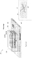
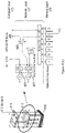
- Figures 1(a)-1(c) illustrate an exemplary computing system 100 including a computing IC 110, a computing IC 120, or a computing IC 140, formed with multiple physical layers that include multiple dies and tiles, in accordance with various embodiments.
- the computing system 100 includes the computing IC 110, which is included in a semiconductor package 103.
- the semiconductor package 103 is placed on a board, e.g., a printed circuit board (PCB), 101.
- the board 101 may include a host or a controller 102, so that the controller 102 and the computing IC 110 may work together to accomplishing desired functions.
- the controller 102 may perform control related operations while the computing device 110 may perform more computation intensive operations, e.g., matrix multiplication.
- the computing IC 110 may be used as a hardware accelerator to the controller 102.
- a computing IC e.g., the computing IC 110, 120, or 140, may be simply referred to as a computing device.
- the computing device 110 may include multiple physical layers, e.g., a physical network layer 107, a physical computing layer 105, and a physical memory layer 109 (hereinafter, simply a network layer 107, a computing layer 105, and a memory layer 109).
- a physical network layer 107 e.g., a physical network layer 107, a physical computing layer 105, and a physical memory layer 109
- other physical layers may be included as well, e.g., a physical power delivery layer, or a physical communication layer, not shown.
- the network layer 107 has a first side and a second side opposite to the first side.
- the computing layer 105 is adjacent to the first side of the network layer 107 and the memory layer 109 is adjacent to the second side of the network layer 107.
- one or more of the network layer 107, the computing layer 105, or the memory layer 109 each includes multiple dies, e.g., a die 112.
- the network layer 107 may include a first set of dies
- the computing layer 105 may include a second set of dies
- the memory layer 109 may include a third set of dies. At least a die of the second set of dies is adjacent to the first side of the network layer 107, and at least a die of the third set of dies is adjacent to the second side of the network layer 107.
- a die of the multiple dies includes multiple tiles, e.g., a tile 114.
- a die of the first set of dies for the network layer 107 includes multiple tiles
- at least a die of the second set of dies for the computing layer 105 includes multiple tiles
- at least a die of the third set of dies for the memory layer 109 includes multiple tiles.
- a tile of the memory layer 109 includes one or more storage cells. In some embodiments, there may be up to about O(10 4 ) tiles on the network layer 107, the computing layer 105, or the memory layer 109.
- the network layer 107 may include a single-hop circuit-switched network to support circuit-switching, where the single-hop circuit-switched network is configured by software.
- the single-hop circuit-switched network may include one or more signal pathways or virtual circuits (VC).
- VC virtual circuits
- the network layer 107 may include a VC 142 starting at a tile 141 and ending at a tile 143, where the VC 142 is a direct, unbuffered signal pathway extending through multiple tiles of the network layer 107.
- the network layer 107 may include one or more signal pathways or VCs, e.g., the VC 142, dynamically configurable between multiple pre-defined topologies for the multiple tiles on the die of the network layer 107.
- the network layer 107 may also include a multi-hop packet switched network to support packet-switching.
- data may move between two tiles in the computing layer 105 or between a tile in the computing layer 105 and a storage cell of the memory layer 109 through a signal pathway of the single-hop circuit-switched network in the network layer 107, or through a path in the multi-hop packet switched network in the network layer 107.
- a tile in the computing layer 105 is arranged to move data to another tile in the computing layer 105 or a storage cell of the memory layer 109 through the one or more signal pathways in the network layer 107.
- the computing IC 120 includes a network layer 127, a computing layer 125, and a memory layer 129, which may be similar to the network layer 107, the computing layer 105, and the memory layer 109.
- the memory layer 129 includes a control logic sublayer 131, and one or more storage cell sublayers 133 having storage cells.
- the network layer 127 or the computing layer 125 may also include one or more sublayers, not shown.
- a sublayer may refer to a single physical layer in a three dimensional grouping of layers.
- the computing IC 140 includes a network layer 147, a computing layer 145, and a memory layer 149, which may be similar to the network layer 107, the computing layer 105, and the memory layer 109.
- the IC 140 further includes an input/output (I/O) layer 148.
- the I/O layer 148 may be placed below memory layer 149. In some other embodiments, the I/O layer 148 may be placed in other locations. There may be further other layers, e.g., a power supply layer, a communication layer, not shown.
- the memory layer 149 includes a control logic sublayer 151, and one or more storage cell sublayers 153 having storage cells.
- the network layer 147, the computing layer 145, or the I/O layer 148 may also include one or more sublayers, not shown.
- dataflow execution model may be applied to the computing device 110.
- the regular design of tiles for the various physical layers may provide a systolic compute fabric leading to inherently stationary latency and throughput.
- the inherently stationary latency and throughput for the computing device 110 may be scale invariant with some small runtime variance.
- the multiple physical layers of the computing device 110 enable shorter distance and low energy interconnect between computing elements and large-capacity memory, compared to an alternative design of placing all the computing elements and large-capacity memory in a same layer.
- 80 fused multiply-add (FMA) computing components may access 64MB of memory positioned within 1.5mm, which may be difficult to achieve for other alternative designs.
- the low frequency design components used in the computing layer 105 can lower the thermal density, enabling three dimensional stacking. Extra-reticle patterning enables 2D scaling via simple repetition.
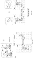
- the network layer 207, the computing layer 205, or the memory layer 209 may be bonded together by direct bonding, where one or more contact points 212 of a first tile in a first layer is in direct contact with one or more contact points of a second tile of a second layer, the first layer or the second layer may be selected from the network layer 207, the computing layer 205, or the memory layer 209.
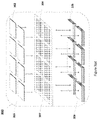
- the computing IC 200 may include one or more tile stacks, e.g., a tile stack 210, which may be viewed as an atomic element of a complete computing system implemented as 3D stack of monolithic layers.
- the tile stack 210 includes a computing tile 215 in the computing layer 205, a network tile 217 in the network layer 207, and a tile 219 in the memory layer 209.
- the computing tile 215, the network tile 217, and the tile 219 in the memory layer 209 may be substantially vertically aligned, one over another.
- the computing tile 215, the network tile 217, and the tile 219 may represent multiple tiles stacked together.
- the tile 219 may include a tile of a control sublayer of the memory layer 209, and one or more storage tiles of one or more storage sublayers of the memory layer 209.
- any of the network layer 207, the computing layer 205, or the memory layer 209 may include multiple dies.
- the network layer 207 has a die 221, a die 223, a die 225, and other dies, which are on a super-reticle.
- Interconnect line 222 may be between the die 221 and the die 223 to couple a first device in the die 221 to a second device of the die 223, or between the die 221 and the die 225 to couple a first device in the die 221 to a second device of the die 225.
- the individual die may be of a size about 20 mm to about 30 mm, while the super-reticle formed for the network layer 207 may be of a size about 50 nm to about 75 mm, which may be 6 times larger than a single die.
- Other physical layers, e.g., the computing layer 205 and the memory layer 209 may be on a super-reticle as well. Additionally and alternatively, the computing layer 205 and the memory layer 209 may be designed differently as showing in Figures 3(a)-3(b) below.
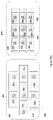
- the computing IC 300 may include the network layer 307 formed on a super-reticle, which may be similar to the super-reticle for the network layer 207 shown in Figure 2 .
- the network layer 307 includes a super-reticle having multiple dies, e.g., a die 304, interconnected by interconnect lines.
- the computing layer 305 or the memory layer 309 may include one or more chiplets, e.g., a chiplet 302, or a chiplet 306.
- a chiplet may be a silicn die in a small form factor.
- a tile of a chiplet may be coupled or bonded to a tile of a die of the super-reticle for the network layer 307.
- the network layer 307 may include multiple tiles 311-318, organized into a radix 6 array shape with multiple rows, e.g., three rows.
- Each tile may have one or more contact points, which may be used for direct bonding or to contact with TSV. All the contact points of a tile are confined to an area less than or equal to 1 ⁇ 2 of the tile, e.g., a left half or a right left that is opposite to the left half of the tile. For example, at a first row, for the tile 316 and the tile 318, the contact points are at the right half of the tile area; at a second row, for the tile 311, the tile 313, and the tile 315, the contact points are at the left half of the tile area.
- the contact points are at the right half of the tile area.
- the pattern of the contact points can be continued for the network layer 307 so that if all the tiles in row n have their contact points on the left half, then all the tiles in row n + 1 have their contact points on the right half.
- the contact points of the tiles for the network layer 307 may result in an interface pattern as seen by other layers, e.g., the compute layer 305 or the memory layer 309 as a Cartesian array.
- the contact points 322 of the tile 312, the contact points 323 of the tile 313, and the contact points 326 of the tile 316 become vertically aligned.
- the contact points 322 of the tile 312 of the network layer 307 may be in direct contact with the contact points 344 of the tile 334 of the computing layer 305
- the contact points 323 of the tile 313 may be in direct contact with the contact points 345 of the tile 335
- the contact points 326 of the tile 316 may be in direct contact with the contact points 346 of the tile 336.
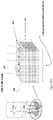
- the dataflow fabric 443 may be an architectural subset of the configurable spatial array dataflow fabric including about 256 PEs, operating with 200 MHz system clock.
- An operation performed by the dataflow fabric 443 may access data stored in the scratch memory 445 embedded in the dataflow fabric 443, or a memory bank in the memory tile 418.
- the bulk of the computing may take place on the dataflow fabric 443 with simplified memory access model.
- the computing tile 414 may have no support for coherency.
- the virtual-physical address translation may be embedded in the control logic of the memory tile 418.
- Input and output to the dataflow fabric 443 can come from the CPU 441, the memory interface 448, the network interface 444, or the VC ports 446.
- the scratch memory 445 within the dataflow fabric 443 may expand capacity and configurability of the dataflow fabric 443.
- VC portals that serve as terminal points or contact points for up to six point-to-point VCs.
- These VC portals can be configured by configuring a selector 442 to act as either a memory portal or a direct extension to the CSA dataflow fabric. In the latter mode, the CPU's on two cooperating tiles can created direct links between their dataflow fabric 443.
- the minimum access granularity for the 8 storage sublayers 453 may be single byte, and maximum transfer rate may be 8 bytes per cycle on each port.
- the memory tile 418 may also support unbuffered, single cycle reads.
- a memory stack configured as 16 banks @ 2MB per bank with a 200MHz system clock may deliver a bandwidth density of 26 GB/s per mm 2 .
- the 600 tiles covering the area of a standard reticle may deliver an aggregate of 15.3 TB/s of access bandwidth operating on 19.3 GB of storage.
- computing element 523 of computing tile 524 in tile stack 520 is configured to be coupled through VC 531 to computing element 513 of computing tile 514 in tile stack 510.
- VC 531 includes a first VC portal 521 of network tile 526 of tile stack 520 and a second VC portal 511 of network tile 516 of tile stack 510.
- Computing element 523 and computing element 513 may be a PE inside a dataflow fabric.
- VC 531 couples computing element 523 in the dataflow fabric in computing tile 524 to computing element 513 in the dataflow fabric in computing tile 514, extending the dataflow fabric from one computing tile to another tile.
- the computing system 100 may employ one or more tile stacks, e.g., tile stack 210, tile stack 410, tile stack 510, or tile stack 520, to perform operations, e.g., matrix-matrix multiplication.
- a performance model for matrix-matrix multiplication illustrates the power of the computing system 100 with the various tile stacks.
- the matrix multiplication operation may be instantiated as a single large dataflow graph and folded directly onto the tile stacks of the computing system 100. In an experiment, throughput is scaled by growing the size of the tile array and by expanding the dataflow graph to utilize the additional tiles. Performance is modeled as the tile array scales from 5K to 40K nodes, achieving 1 PFlop/s sustained performance at approximately 34K nodes.
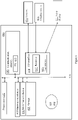
- the system 600 may include one or more processors 602, and one or more hardware accelerators 603.
- the hardware accelerator 603 may be an example of the computing IC 110, 120, 140, as shown in Figures 1(a)-1(c) , the computing IC 200 as shown in Figure 2 , the computing IC 300 as shown in Figures 3(a)-3(b) , with further details of a computing IC as shown in Figures 4(a)-4(d) , and in Figures 5(a)-5(c) .
- a software module 663 may be executed by the execution unit(s) 602.
- the computing system 600 may include a main memory device 604, which may be any one of a number of known persistent storage media, and a data storage circuitry 608.
- memory circuitry 604 can be any suitable type, number and/or combination of volatile memory devices (e.g., random access memory (RAM), dynamic RAM (DRAM), static RAM (SRAM), etc.) and/or non-volatile memory devices (e.g., read-only memory (ROM), erasable programmable read-only memory (EPROM), electrically erasable programmable read-only memory (EEPROM), flash memory, antifuses, etc.) that may be configured in any suitable implementation as are known.
- volatile memory devices e.g., random access memory (RAM), dynamic RAM (DRAM), static RAM (SRAM), etc.
- non-volatile memory devices e.g., read-only memory (ROM), erasable programmable read-only memory (EPROM), electrically erasable programmable read-only memory (EEPROM), flash memory, antifuses, etc.
- ROM read-only memory
- EPROM erasable programmable read-only memory
- EEPROM electrically erasable programmable read
- the number, capability and/or capacity of these elements 602-663 may vary, depending on the number of other devices the device 600 is configured to support. Otherwise, the constitutions of elements 602-661 are known, and accordingly will not be further described.
- a computer-usable or computer-readable medium could even be paper or another suitable medium upon which the program is printed, as the program can be electronically captured, via, for instance, optical scanning of the paper or other medium, then compiled, interpreted, or otherwise processed in a suitable manner, if necessary, and then stored in a computer memory.
- a computer-usable or computer-readable medium may be any medium that can contain, store, communicate, propagate, or transport the program for use by or in connection with the instruction execution system, apparatus, or device.
- the computer-usable medium may include a propagated data signal with the computer-usable program code embodied therewith, either in baseband or as part of a carrier wave.
- the computer usable program code may be transmitted using any appropriate medium, including but not limited to wireless, wireline, optical fiber cable, RF, etc.
Landscapes
- Engineering & Computer Science (AREA)
- Theoretical Computer Science (AREA)
- Physics & Mathematics (AREA)
- Computer Hardware Design (AREA)
- General Engineering & Computer Science (AREA)
- General Physics & Mathematics (AREA)
- Software Systems (AREA)
- Power Engineering (AREA)
- Human Computer Interaction (AREA)
- Semiconductor Memories (AREA)
- Geometry (AREA)
- Design And Manufacture Of Integrated Circuits (AREA)
Claims (13)
- Integrierte Schaltung (110, 120, 140), umfassend:eine physische Netzwerkschicht (107, 127, 147), die einen ersten Satz von Dies (112), der zum Ausführen von Funktionen konfiguriert ist, die mit Vernetzung assoziiert sind, eine erste Seite und eine zweite Seite gegenüber der ersten Seite aufweist, wobei ein Die des ersten Satzes von Dies mehrere Tiles (114) umfasst, wobei die physische Netzwerkschicht ferner einen oder mehrere Signalwege umfasst, die dynamisch konfigurierbar sind, um jeweilige virtuelle Schaltungen, VCs, zu definieren, die mit jeweiligen vordefinierten Zwischenverbindungstopologien assoziiert sind, um dadurch verschiedene Sätze von Tiles der mehreren Tiles miteinander zu verbinden, wobei jede Topologie der mehreren vordefinierten Zwischenverbindungstopologien einem Kommunikationsmuster entspricht, das mit einer Workload in Beziehung steht;eine physische Datenverarbeitungsschicht (105, 125, 145) mit einem zweiten Satz von Dies (112), der zum Ausführen von Funktionen konfiguriert ist, die mit Datenverarbeitung assoziiert sind, wobei mindestens ein Die des zweiten Satzes von Dies benachbart zur ersten Seite der physischen Netzwerkschicht ist oder mehrere Tiles (114) umfasst; undeine physische Speicherschicht (109, 129, 149) mit einem dritten Satz von Dies (112), der zum Ausführen von Funktionen konfiguriert ist, die mit Speicherverarbeitung assoziiert sind, wobei mindestens ein Die des dritten Satzes von Dies benachbart zur zweiten Seite der physischen Netzwerkschicht ist, wobei mindestens ein Die des dritten Satzes von Dies mehrere Tiles umfasst (114), und ein Tile der physischen Speicherschicht eine oder mehrere Speicherzellen umfasst; undwobei mindestens ein Tile der physischen Datenverarbeitungsschicht ferner zum Verschieben von Daten durch mindestens eine VC, die durch den einen oder die mehreren Signalwege in der physischen Netzwerkschicht definiert ist, in einen anderen Tile in der physischen Datenverarbeitungsschicht oder eine Speicherzelle der physischen Speicherschicht ausgelegt ist.
- Integrierte Schaltung nach Anspruch 1, wobei die physische Netzwerkschicht, die physische Datenverarbeitungsschicht und die physische Speicherschicht durch durchgehende Silizium-Durchkontaktierungen, TSV, selektiv miteinander gekoppelt oder durch Direktbonden aneinander gebondet sind, wobei eine oder mehrere Kontaktstellen eines ersten Tiles in einer ersten der physischen Netzwerk-, Datenverarbeitungs- und Speicherschicht in direktem Kontakt mit einer oder mehreren Kontaktstellen eines zweiten Tiles einer zweiten der physischen Netzwerk-, Datenverarbeitungs- und Speicherschicht stehen.
- Integrierte Schaltung nach einem der Ansprüche 1 bis 2, wobei mindestens eine der physischen Netzwerkschicht, der physischen Datenverarbeitungsschicht oder der physischen Speicherschicht ein Super-Retikel mit mehreren Dies umfasst, die durch Zwischenverbindungsleitungen, die ein erstes Bauelement in einem ersten Die der mehreren Dies mit einem zweiten Bauelement eines zweiten Dies der mehreren Dies koppeln, miteinander verbunden sind.
- Integrierte Schaltung nach einem der Ansprüche 1 bis 2, wobei die physische Netzwerkschicht ein paketvermitteltes Mehrsprung-Netzwerk zum Unterstützen von Paketvermittlung oder ein konfigurierbares leitungsvermitteltes Einsprung-Netzwerk zum Unterstützen von Leitungsvermittlung umfasst.
- Integrierte Schaltung nach einem der Ansprüche 1 bis 2, wobei ein Tile der physischen Datenverarbeitungsschicht eine Eingabe-/Ausgabe-, E-/A-, Schnittstelle, eine Speicherschnittstelle, einen Scratch-Speicher, Zwischenverbindungen oder ein Datenverarbeitungselement umfasst, das aus einem Prozessorkern, einem konfigurierbaren räumlichen Array, CSA, einer anwendungsspezifischen integrierten Schaltung, ASIC, einer zentralen Verarbeitungseinheit, CPU, einer Verarbeitungs-Engine, PE, oder einer Datenfluss-Fabric ausgewählt ist.
- Integrierte Schaltung nach Anspruch 5, wobei die E-/A-Schnittstelle des Tiles der physischen Datenverarbeitungsschicht ein oder mehrere Portale zur physischen Speicherschicht, ein oder mehrere Portale zu einem paketvermittelten Mehrsprung-Netzwerk der physischen Netzwerkschicht oder ein oder mehrere Portale zu einem leitungsvermittelten Einsprung-Netzwerk der physischen Netzwerkschicht umfasst, und wobei die physische Netzwerkschicht das paketvermittelte Mehrsprung-Netzwerk zum Unterstützen von Paketvermittlung und das leitungsvermittelte Einsprung-Netzwerk zum Unterstützen von Leitungsvermittlung umfasst.
- Integrierte Schaltung nach einem der Ansprüche 1 bis 2, wobei die integrierte Schaltung einen oder mehrere Tile-Stapel (210) umfasst, wobei ein Tile-Stapel des einen oder der mehreren Tile-Stapel einen Datenverarbeitungs-Tile in der physischen Datenverarbeitungsschicht, einen Netzwerk-Tile in der physischen Netzwerkschicht, einen Tile einer Steuerungsteilschicht der physischen Speicherschicht und einen oder mehrere Speicherungs-Tiles einer oder mehrerer Speicherungsteilschichten der physischen Speicherschicht umfasst, wobei der Datenverarbeitungs-Tile, der Netzwerk-Tile, der Tile einer Steuerungsteilschicht und der eine oder die mehreren Speicherungs-Tiles so konfiguriert sind, dass sie im Wesentlichen vertikal ausgerichtet sind, und wobei:der Datenverarbeitungs-Tile eine Eingabe-/Ausgabe-, E-/A-, Schnittstelle, eine Speicherschnittstelle, einen Scratch-Speicher, Zwischenverbindungen und mindestens ein Datenverarbeitungselement umfasst, das aus einem Prozessorkern, einem konfigurierbaren räumlichen Array, CSA, einer anwendungsspezifischen integrierten Schaltung, ASIC, einer zentralen Verarbeitungseinheit, CPU, einer Verarbeitungs-Engine, PE, oder einer Datenfluss-Fabric ausgewählt ist;der Netzwerk-Tile ein Portal einer virtuellen Schaltung, VC, umfasst, das so konfiguriert ist, dass es ein Segment einer virtuellen Schaltung in der physischen Netzwerkschicht für ein leitungsvermitteltes Einsprung-Netzwerk zum Unterstützen von Leitungsvermittlung bildet; oderder eine oder die mehreren Speicherungs-Tiles mehrere Speicherzellen umfassen.
- Integrierte Schaltung nach Anspruch 7, wobei ein Datenverarbeitungselement des Datenverarbeitungs-Tiles eines ersten Tile-Stapels des einen oder der mehreren Tile-Stapel so konfiguriert ist, dass es Speicherzugriff auf eine oder mehrere Speicherzellen eines oder mehrerer Speicherungs-Tiles eines zweiten Tile-Stapels hat, wobei der Speicherzugriff durch das Datenverarbeitungselement über ein VC-Portal des Netzwerk-Tiles des ersten Tile-Stapels und ein VC-Portal des Netzwerk-Tiles des zweiten Tile-Stapels erfolgt.
- Integrierte Schaltung nach einem der Ansprüche 7 bis 8, wobei ein erstes Datenverarbeitungselement des Datenverarbeitungs-Tiles eines ersten Tile-Stapels des einen oder der mehreren Tile-Stapel so konfiguriert ist, dass es über eine VC mit einem zweiten Datenverarbeitungselement des Datenverarbeitungs-Tiles eines zweiten Tile-Stapels des einen oder der mehreren Tile-Stapel gekoppelt ist, wobei die VC ein erstes VC-Portal des Netzwerk-Tiles des ersten Tile-Stapels und ein zweites VC-Portal des Netzwerk-Tiles des zweiten Tile-Stapels umfasst.
- Datenverarbeitungssystem (100), umfassend:eine gedruckte Leiterplatte, PCB, (101);einen Host (102), der an der PCB angebracht ist; undein Halbleiter-Package (103), das die integrierte Schaltung (110, 120, 140) nach einem der Ansprüche 1 bis 9 umfasst,wobei der Host und das Halbleiter-Package auf der PCB angeordnet sind, die Speicherschicht der integrierten Schaltung näher zu einer oberen Oberfläche der PCB ist als die Datenverarbeitungsschicht der integrierten Schaltung, und die obere Oberfläche als die Oberfläche der PCB in Kontakt mit dem Halbleiter-Package definiert ist.
- Datenverarbeitungssystem nach Anspruch 10, wobei die physische Netzwerkschicht ein Super-Retikel mit mehreren Dies umfasst, die durch Zwischenverbindungsleitungen, die ein erstes Bauelement in einem ersten Die der mehreren Dies mit einem zweiten Bauelement eines zweiten Dies der mehreren Dies koppeln, miteinander verbunden sind, und die physische Datenverarbeitungsschicht oder die physische Speicherschicht ein oder mehrere Chiplets umfasst, wobei ein Tile eines Chiplets des einen oder der mehreren Chiplets an einen Tile eines Dies des Super-Retikels für die physische Netzwerkschicht gebondet ist.
- Datenverarbeitungssystem nach einem der Ansprüche 10 bis 11, wobei die physische Netzwerkschicht mehrere Tiles aufweist, die in einer Basis-6-Array-Form mit mehreren Zeilen organisiert sind, wobei ein Tile in einer ersten Zeile eine oder mehrere Kontaktstellen aufweist, die sich in einer ersten Hälfte des Tiles befinden, und ein Tile in einer zweiten Zeile benachbart zur ersten Zeile eine oder mehrere Kontaktstellen aufweist, die sich in einer zweiten Hälfte des Tiles gegenüber der ersten Hälfte des Tiles befinden, und wobei die physische Datenverarbeitungsschicht oder die physische Speicherschicht mehrere Tiles aufweisen, die in einer Basis-4-Array-Form in einem standardmäßigen NEWS-Gitter organisiert sind, wobei eine oder mehrere Kontaktstellen eines ersten Tiles in der physischen Netzwerkschicht mit einer oder mehreren Kontaktstellen eines zweiten Tiles der physischen Datenverarbeitungsschicht oder physischen Speicherschicht in direktem Kontakt stehen.
- Datenverarbeitungssystem nach einem der Ansprüche 10 bis 11, wobei ein Tile der physischen Datenverarbeitungsschicht eine Eingabe-/Ausgabe-, E-/A-, Schnittstelle, eine Speicherschnittstelle, einen Scratch-Speicher, Zwischenverbindungen oder ein Datenverarbeitungselement umfasst, das aus einem Prozessorkern, einem konfigurierbaren räumlichen Array, CSA, einer anwendungsspezifischen integrierten Schaltung, ASIC, einer zentralen Verarbeitungseinheit, CPU, einer Verarbeitungs-Engine, PE, oder einer Datenfluss-Fabric ausgewählt ist.
Applications Claiming Priority (1)
| Application Number | Priority Date | Filing Date | Title |
|---|---|---|---|
| US16/416,753 US10691182B2 (en) | 2019-05-20 | 2019-05-20 | Layered super-reticle computing: architectures and methods |
Publications (2)
| Publication Number | Publication Date |
|---|---|
| EP3742485A1 EP3742485A1 (de) | 2020-11-25 |
| EP3742485B1 true EP3742485B1 (de) | 2022-08-24 |
Family
ID=68532851
Family Applications (1)
| Application Number | Title | Priority Date | Filing Date |
|---|---|---|---|
| EP20166445.5A Active EP3742485B1 (de) | 2019-05-20 | 2020-03-27 | Geschichtetes super-retikel-computing: architekturen und verfahren |
Country Status (2)
| Country | Link |
|---|---|
| US (3) | US10691182B2 (de) |
| EP (1) | EP3742485B1 (de) |
Families Citing this family (10)
| Publication number | Priority date | Publication date | Assignee | Title |
|---|---|---|---|---|
| US10854763B2 (en) * | 2018-09-17 | 2020-12-01 | Gbt Technologies Inc. | Multi-dimensional integrated circuit having multiple planes and memory architecture having a honeycomb or bee hive structure |
| US11139283B2 (en) * | 2018-12-22 | 2021-10-05 | Xcelsis Corporation | Abstracted NAND logic in stacks |
| US11264361B2 (en) * | 2019-06-05 | 2022-03-01 | Invensas Corporation | Network on layer enabled architectures |
| WO2021108090A1 (en) * | 2019-11-26 | 2021-06-03 | Mythic, Inc. | Systems and methods for implementing redundancy for tile-based intelligence processing computing architecture |
| US11226816B2 (en) * | 2020-02-12 | 2022-01-18 | Samsung Electronics Co., Ltd. | Systems and methods for data placement for in-memory-compute |
| KR102898250B1 (ko) * | 2021-01-26 | 2025-12-11 | 삼성전자주식회사 | 멀티 레벨 시그널링을 이용하는 고대역폭 메모리 시스템 |
| US11488935B1 (en) * | 2021-05-07 | 2022-11-01 | Applied Materials, Inc. | Scalable network-on-package for connecting chiplet-based designs |
| KR20230095685A (ko) * | 2021-12-22 | 2023-06-29 | 삼성전자주식회사 | 반도체 패키지 |
| US20250259685A1 (en) * | 2024-02-13 | 2025-08-14 | Sandisk Technologies Llc | High bandwidth nonvolatile memory devices |
| TW202545043A (zh) * | 2024-03-29 | 2025-11-16 | 美商谷歌有限責任公司 | 無矽穿孔情況下之記憶體與計算3dic整合 |
Family Cites Families (11)
| Publication number | Priority date | Publication date | Assignee | Title |
|---|---|---|---|---|
| KR20080067328A (ko) * | 2005-09-06 | 2008-07-18 | 비욘드 블라데스 리미티드 | 3dmc 아키텍처 |
| US8796740B1 (en) * | 2009-01-13 | 2014-08-05 | Altera Corporation | Using a single mask for various design configurations |
| WO2011107612A1 (en) * | 2010-03-05 | 2011-09-09 | Imec | Customizable interconnections between electronic circuits |
| US9026872B2 (en) * | 2012-08-16 | 2015-05-05 | Xilinx, Inc. | Flexible sized die for use in multi-die integrated circuit |
| US9886193B2 (en) | 2015-05-15 | 2018-02-06 | International Business Machines Corporation | Architecture and implementation of cortical system, and fabricating an architecture using 3D wafer scale integration |
| US10075524B1 (en) * | 2015-09-29 | 2018-09-11 | Amazon Technologies, Inc. | Storage bridge device for communicating with network storage |
| KR101843397B1 (ko) * | 2016-08-03 | 2018-03-30 | 한국전자통신연구원 | 반도체 장치 및 반도체 패키지 |
| KR101942727B1 (ko) * | 2016-09-12 | 2019-01-28 | 삼성전기 주식회사 | 팬-아웃 반도체 패키지 |
| US10468397B2 (en) * | 2017-05-05 | 2019-11-05 | X-Celeprint Limited | Matrix addressed tiles and arrays |
| US10469397B2 (en) * | 2017-07-01 | 2019-11-05 | Intel Corporation | Processors and methods with configurable network-based dataflow operator circuits |
| US10963780B2 (en) * | 2017-08-24 | 2021-03-30 | Google Llc | Yield improvements for three-dimensionally stacked neural network accelerators |
-
2019
- 2019-05-20 US US16/416,753 patent/US10691182B2/en active Active
-
2020
- 2020-03-27 EP EP20166445.5A patent/EP3742485B1/de active Active
- 2020-04-29 US US16/862,263 patent/US10963022B2/en active Active
-
2021
- 2021-02-11 US US17/174,106 patent/US11656662B2/en active Active
Also Published As
| Publication number | Publication date |
|---|---|
| US20210255674A1 (en) | 2021-08-19 |
| US20190354146A1 (en) | 2019-11-21 |
| US11656662B2 (en) | 2023-05-23 |
| US10691182B2 (en) | 2020-06-23 |
| EP3742485A1 (de) | 2020-11-25 |
| US20200371566A1 (en) | 2020-11-26 |
| US10963022B2 (en) | 2021-03-30 |
Similar Documents
| Publication | Publication Date | Title |
|---|---|---|
| US11656662B2 (en) | Layered super-reticle computing : architectures and methods | |
| Adiga et al. | An overview of the BlueGene/L supercomputer | |
| US12260118B2 (en) | Deterministic near-compute memory for deterministic processor and enhanced data movement between memory units and processing units | |
| US9825843B2 (en) | Die-stacked device with partitioned multi-hop network | |
| Shao et al. | Simba: scaling deep-learning inference with chiplet-based architecture | |
| TW202305623A (zh) | 存算一體裝置及相關的方法 | |
| Xie et al. | Die-stacking architecture | |
| Sharma et al. | A heterogeneous chiplet architecture for accelerating end-to-end transformer models | |
| US9003160B2 (en) | Active buffered memory | |
| Jiao et al. | FPIA: Communication-aware multi-chiplet integration with field-programmable interconnect fabric on reusable silicon interposer | |
| Kurshan et al. | 3d stacking for ai systems: Emulating heterogeneous 3d architectures for ai | |
| US9257152B2 (en) | Memory architectures having wiring structures that enable different access patterns in multiple dimensions | |
| US20230418604A1 (en) | Reconfigurable vector processing in a memory | |
| Jagasivamani et al. | Memory-systems challenges in realizing monolithic computers | |
| Koob et al. | Design of a 3-D fully depleted SOI computational RAM | |
| Kurshan et al. | Towards 3D AI hardware: fine-grain hardware characterization of 3D stacks for heterogeneous system integration & AI systems | |
| US12572342B2 (en) | Configurable access to a reconfigurable processor by a virtual function | |
| Bhanota et al. | The bluegene/l supercomputer | |
| Lee et al. | 16.2 rngd: A 5nm tensor-contraction processor for power-efficient inference on large language models | |
| JPH0636060A (ja) | スライド・ネットワークに使用するアレイ・プロセッサ | |
| Gannavaram et al. | Performance Analysis of 3D Stacked Memory Architectures in High Performance Computing | |
| Balaji et al. | Understanding network saturation behavior on large-scale blue gene/p systems | |
| Barrett et al. | An overview of the BlueGene/L supercomputer | |
| Clermidy et al. | 3D stacking for multi-core architectures: From WIDEIO to distributed caches | |
| US12482756B2 (en) | Connectivity layer in 3D devices |
Legal Events
| Date | Code | Title | Description |
|---|---|---|---|
| PUAI | Public reference made under article 153(3) epc to a published international application that has entered the european phase |
Free format text: ORIGINAL CODE: 0009012 |
|
| STAA | Information on the status of an ep patent application or granted ep patent |
Free format text: STATUS: THE APPLICATION HAS BEEN PUBLISHED |
|
| AK | Designated contracting states |
Kind code of ref document: A1 Designated state(s): AL AT BE BG CH CY CZ DE DK EE ES FI FR GB GR HR HU IE IS IT LI LT LU LV MC MK MT NL NO PL PT RO RS SE SI SK SM TR |
|
| AX | Request for extension of the european patent |
Extension state: BA ME |
|
| STAA | Information on the status of an ep patent application or granted ep patent |
Free format text: STATUS: REQUEST FOR EXAMINATION WAS MADE |
|
| 17P | Request for examination filed |
Effective date: 20210520 |
|
| RBV | Designated contracting states (corrected) |
Designated state(s): AL AT BE BG CH CY CZ DE DK EE ES FI FR GB GR HR HU IE IS IT LI LT LU LV MC MK MT NL NO PL PT RO RS SE SI SK SM TR |
|
| GRAP | Despatch of communication of intention to grant a patent |
Free format text: ORIGINAL CODE: EPIDOSNIGR1 |
|
| STAA | Information on the status of an ep patent application or granted ep patent |
Free format text: STATUS: GRANT OF PATENT IS INTENDED |
|
| RIC1 | Information provided on ipc code assigned before grant |
Ipc: H01L 25/18 20060101AFI20220224BHEP |
|
| INTG | Intention to grant announced |
Effective date: 20220314 |
|
| GRAS | Grant fee paid |
Free format text: ORIGINAL CODE: EPIDOSNIGR3 |
|
| GRAA | (expected) grant |
Free format text: ORIGINAL CODE: 0009210 |
|
| STAA | Information on the status of an ep patent application or granted ep patent |
Free format text: STATUS: THE PATENT HAS BEEN GRANTED |
|
| AK | Designated contracting states |
Kind code of ref document: B1 Designated state(s): AL AT BE BG CH CY CZ DE DK EE ES FI FR GB GR HR HU IE IS IT LI LT LU LV MC MK MT NL NO PL PT RO RS SE SI SK SM TR |
|
| REG | Reference to a national code |
Ref country code: CH Ref legal event code: EP |
|
| REG | Reference to a national code |
Ref country code: IE Ref legal event code: FG4D |
|
| REG | Reference to a national code |
Ref country code: AT Ref legal event code: REF Ref document number: 1514244 Country of ref document: AT Kind code of ref document: T Effective date: 20220915 Ref country code: DE Ref legal event code: R096 Ref document number: 602020004638 Country of ref document: DE |
|
| REG | Reference to a national code |
Ref country code: NL Ref legal event code: FP |
|
| REG | Reference to a national code |
Ref country code: LT Ref legal event code: MG9D |
|
| PG25 | Lapsed in a contracting state [announced via postgrant information from national office to epo] |
Ref country code: SE Free format text: LAPSE BECAUSE OF FAILURE TO SUBMIT A TRANSLATION OF THE DESCRIPTION OR TO PAY THE FEE WITHIN THE PRESCRIBED TIME-LIMIT Effective date: 20220824 Ref country code: RS Free format text: LAPSE BECAUSE OF FAILURE TO SUBMIT A TRANSLATION OF THE DESCRIPTION OR TO PAY THE FEE WITHIN THE PRESCRIBED TIME-LIMIT Effective date: 20220824 Ref country code: PT Free format text: LAPSE BECAUSE OF FAILURE TO SUBMIT A TRANSLATION OF THE DESCRIPTION OR TO PAY THE FEE WITHIN THE PRESCRIBED TIME-LIMIT Effective date: 20221226 Ref country code: NO Free format text: LAPSE BECAUSE OF FAILURE TO SUBMIT A TRANSLATION OF THE DESCRIPTION OR TO PAY THE FEE WITHIN THE PRESCRIBED TIME-LIMIT Effective date: 20221124 Ref country code: LV Free format text: LAPSE BECAUSE OF FAILURE TO SUBMIT A TRANSLATION OF THE DESCRIPTION OR TO PAY THE FEE WITHIN THE PRESCRIBED TIME-LIMIT Effective date: 20220824 Ref country code: LT Free format text: LAPSE BECAUSE OF FAILURE TO SUBMIT A TRANSLATION OF THE DESCRIPTION OR TO PAY THE FEE WITHIN THE PRESCRIBED TIME-LIMIT Effective date: 20220824 Ref country code: FI Free format text: LAPSE BECAUSE OF FAILURE TO SUBMIT A TRANSLATION OF THE DESCRIPTION OR TO PAY THE FEE WITHIN THE PRESCRIBED TIME-LIMIT Effective date: 20220824 |
|
| REG | Reference to a national code |
Ref country code: AT Ref legal event code: MK05 Ref document number: 1514244 Country of ref document: AT Kind code of ref document: T Effective date: 20220824 |
|
| PG25 | Lapsed in a contracting state [announced via postgrant information from national office to epo] |
Ref country code: PL Free format text: LAPSE BECAUSE OF FAILURE TO SUBMIT A TRANSLATION OF THE DESCRIPTION OR TO PAY THE FEE WITHIN THE PRESCRIBED TIME-LIMIT Effective date: 20220824 Ref country code: IS Free format text: LAPSE BECAUSE OF FAILURE TO SUBMIT A TRANSLATION OF THE DESCRIPTION OR TO PAY THE FEE WITHIN THE PRESCRIBED TIME-LIMIT Effective date: 20221224 Ref country code: HR Free format text: LAPSE BECAUSE OF FAILURE TO SUBMIT A TRANSLATION OF THE DESCRIPTION OR TO PAY THE FEE WITHIN THE PRESCRIBED TIME-LIMIT Effective date: 20220824 Ref country code: GR Free format text: LAPSE BECAUSE OF FAILURE TO SUBMIT A TRANSLATION OF THE DESCRIPTION OR TO PAY THE FEE WITHIN THE PRESCRIBED TIME-LIMIT Effective date: 20221125 |
|
| PG25 | Lapsed in a contracting state [announced via postgrant information from national office to epo] |
Ref country code: SM Free format text: LAPSE BECAUSE OF FAILURE TO SUBMIT A TRANSLATION OF THE DESCRIPTION OR TO PAY THE FEE WITHIN THE PRESCRIBED TIME-LIMIT Effective date: 20220824 Ref country code: RO Free format text: LAPSE BECAUSE OF FAILURE TO SUBMIT A TRANSLATION OF THE DESCRIPTION OR TO PAY THE FEE WITHIN THE PRESCRIBED TIME-LIMIT Effective date: 20220824 Ref country code: ES Free format text: LAPSE BECAUSE OF FAILURE TO SUBMIT A TRANSLATION OF THE DESCRIPTION OR TO PAY THE FEE WITHIN THE PRESCRIBED TIME-LIMIT Effective date: 20220824 Ref country code: DK Free format text: LAPSE BECAUSE OF FAILURE TO SUBMIT A TRANSLATION OF THE DESCRIPTION OR TO PAY THE FEE WITHIN THE PRESCRIBED TIME-LIMIT Effective date: 20220824 Ref country code: CZ Free format text: LAPSE BECAUSE OF FAILURE TO SUBMIT A TRANSLATION OF THE DESCRIPTION OR TO PAY THE FEE WITHIN THE PRESCRIBED TIME-LIMIT Effective date: 20220824 Ref country code: AT Free format text: LAPSE BECAUSE OF FAILURE TO SUBMIT A TRANSLATION OF THE DESCRIPTION OR TO PAY THE FEE WITHIN THE PRESCRIBED TIME-LIMIT Effective date: 20220824 |
|
| REG | Reference to a national code |
Ref country code: DE Ref legal event code: R097 Ref document number: 602020004638 Country of ref document: DE |
|
| PG25 | Lapsed in a contracting state [announced via postgrant information from national office to epo] |
Ref country code: SK Free format text: LAPSE BECAUSE OF FAILURE TO SUBMIT A TRANSLATION OF THE DESCRIPTION OR TO PAY THE FEE WITHIN THE PRESCRIBED TIME-LIMIT Effective date: 20220824 Ref country code: EE Free format text: LAPSE BECAUSE OF FAILURE TO SUBMIT A TRANSLATION OF THE DESCRIPTION OR TO PAY THE FEE WITHIN THE PRESCRIBED TIME-LIMIT Effective date: 20220824 |
|
| P01 | Opt-out of the competence of the unified patent court (upc) registered |
Effective date: 20230518 |
|
| PG25 | Lapsed in a contracting state [announced via postgrant information from national office to epo] |
Ref country code: AL Free format text: LAPSE BECAUSE OF FAILURE TO SUBMIT A TRANSLATION OF THE DESCRIPTION OR TO PAY THE FEE WITHIN THE PRESCRIBED TIME-LIMIT Effective date: 20220824 |
|
| PLBE | No opposition filed within time limit |
Free format text: ORIGINAL CODE: 0009261 |
|
| STAA | Information on the status of an ep patent application or granted ep patent |
Free format text: STATUS: NO OPPOSITION FILED WITHIN TIME LIMIT |
|
| 26N | No opposition filed |
Effective date: 20230525 |
|
| PG25 | Lapsed in a contracting state [announced via postgrant information from national office to epo] |
Ref country code: SI Free format text: LAPSE BECAUSE OF FAILURE TO SUBMIT A TRANSLATION OF THE DESCRIPTION OR TO PAY THE FEE WITHIN THE PRESCRIBED TIME-LIMIT Effective date: 20220824 |
|
| PG25 | Lapsed in a contracting state [announced via postgrant information from national office to epo] |
Ref country code: MC Free format text: LAPSE BECAUSE OF FAILURE TO SUBMIT A TRANSLATION OF THE DESCRIPTION OR TO PAY THE FEE WITHIN THE PRESCRIBED TIME-LIMIT Effective date: 20220824 |
|
| REG | Reference to a national code |
Ref country code: CH Ref legal event code: PL |
|
| REG | Reference to a national code |
Ref country code: BE Ref legal event code: MM Effective date: 20230331 |
|
| PG25 | Lapsed in a contracting state [announced via postgrant information from national office to epo] |
Ref country code: LU Free format text: LAPSE BECAUSE OF NON-PAYMENT OF DUE FEES Effective date: 20230327 |
|
| REG | Reference to a national code |
Ref country code: IE Ref legal event code: MM4A |
|
| PG25 | Lapsed in a contracting state [announced via postgrant information from national office to epo] |
Ref country code: LI Free format text: LAPSE BECAUSE OF NON-PAYMENT OF DUE FEES Effective date: 20230331 Ref country code: IE Free format text: LAPSE BECAUSE OF NON-PAYMENT OF DUE FEES Effective date: 20230327 Ref country code: FR Free format text: LAPSE BECAUSE OF NON-PAYMENT OF DUE FEES Effective date: 20230331 Ref country code: CH Free format text: LAPSE BECAUSE OF NON-PAYMENT OF DUE FEES Effective date: 20230331 |
|
| PG25 | Lapsed in a contracting state [announced via postgrant information from national office to epo] |
Ref country code: BE Free format text: LAPSE BECAUSE OF NON-PAYMENT OF DUE FEES Effective date: 20230331 |
|
| PG25 | Lapsed in a contracting state [announced via postgrant information from national office to epo] |
Ref country code: IT Free format text: LAPSE BECAUSE OF FAILURE TO SUBMIT A TRANSLATION OF THE DESCRIPTION OR TO PAY THE FEE WITHIN THE PRESCRIBED TIME-LIMIT Effective date: 20220824 |
|
| PG25 | Lapsed in a contracting state [announced via postgrant information from national office to epo] |
Ref country code: BG Free format text: LAPSE BECAUSE OF FAILURE TO SUBMIT A TRANSLATION OF THE DESCRIPTION OR TO PAY THE FEE WITHIN THE PRESCRIBED TIME-LIMIT Effective date: 20220824 |
|
| GBPC | Gb: european patent ceased through non-payment of renewal fee |
Effective date: 20240327 |
|
| PG25 | Lapsed in a contracting state [announced via postgrant information from national office to epo] |
Ref country code: BG Free format text: LAPSE BECAUSE OF FAILURE TO SUBMIT A TRANSLATION OF THE DESCRIPTION OR TO PAY THE FEE WITHIN THE PRESCRIBED TIME-LIMIT Effective date: 20220824 |
|
| PG25 | Lapsed in a contracting state [announced via postgrant information from national office to epo] |
Ref country code: GB Free format text: LAPSE BECAUSE OF NON-PAYMENT OF DUE FEES Effective date: 20240327 |
|
| PG25 | Lapsed in a contracting state [announced via postgrant information from national office to epo] |
Ref country code: GB Free format text: LAPSE BECAUSE OF NON-PAYMENT OF DUE FEES Effective date: 20240327 |
|
| PG25 | Lapsed in a contracting state [announced via postgrant information from national office to epo] |
Ref country code: CY Free format text: LAPSE BECAUSE OF FAILURE TO SUBMIT A TRANSLATION OF THE DESCRIPTION OR TO PAY THE FEE WITHIN THE PRESCRIBED TIME-LIMIT; INVALID AB INITIO Effective date: 20200327 |
|
| PG25 | Lapsed in a contracting state [announced via postgrant information from national office to epo] |
Ref country code: HU Free format text: LAPSE BECAUSE OF FAILURE TO SUBMIT A TRANSLATION OF THE DESCRIPTION OR TO PAY THE FEE WITHIN THE PRESCRIBED TIME-LIMIT; INVALID AB INITIO Effective date: 20200327 |
|
| REG | Reference to a national code |
Ref country code: DE Ref legal event code: R079 Ref document number: 602020004638 Country of ref document: DE Free format text: PREVIOUS MAIN CLASS: H01L0025180000 Ipc: H10W0090000000 |
|
| PG25 | Lapsed in a contracting state [announced via postgrant information from national office to epo] |
Ref country code: TR Free format text: LAPSE BECAUSE OF FAILURE TO SUBMIT A TRANSLATION OF THE DESCRIPTION OR TO PAY THE FEE WITHIN THE PRESCRIBED TIME-LIMIT Effective date: 20220824 |
|
| PGFP | Annual fee paid to national office [announced via postgrant information from national office to epo] |
Ref country code: NL Payment date: 20260227 Year of fee payment: 7 |
|
| PGFP | Annual fee paid to national office [announced via postgrant information from national office to epo] |
Ref country code: DE Payment date: 20260102 Year of fee payment: 7 |