EP3740048A1 - Wiring board and manufacturing method thereof - Google Patents
Wiring board and manufacturing method thereof Download PDFInfo
- Publication number
- EP3740048A1 EP3740048A1 EP20166816.7A EP20166816A EP3740048A1 EP 3740048 A1 EP3740048 A1 EP 3740048A1 EP 20166816 A EP20166816 A EP 20166816A EP 3740048 A1 EP3740048 A1 EP 3740048A1
- Authority
- EP
- European Patent Office
- Prior art keywords
- insulating substrate
- wiring board
- protruding parts
- connection pads
- parts
- Prior art date
- Legal status (The legal status is an assumption and is not a legal conclusion. Google has not performed a legal analysis and makes no representation as to the accuracy of the status listed.)
- Granted
Links
Images





Classifications
-
- H—ELECTRICITY
- H05—ELECTRIC TECHNIQUES NOT OTHERWISE PROVIDED FOR
- H05K—PRINTED CIRCUITS; CASINGS OR CONSTRUCTIONAL DETAILS OF ELECTRIC APPARATUS; MANUFACTURE OF ASSEMBLAGES OF ELECTRICAL COMPONENTS
- H05K1/00—Printed circuits
- H05K1/02—Details
- H05K1/11—Printed elements for providing electric connections to or between printed circuits
- H05K1/111—Pads for surface mounting, e.g. lay-out
-
- H—ELECTRICITY
- H05—ELECTRIC TECHNIQUES NOT OTHERWISE PROVIDED FOR
- H05K—PRINTED CIRCUITS; CASINGS OR CONSTRUCTIONAL DETAILS OF ELECTRIC APPARATUS; MANUFACTURE OF ASSEMBLAGES OF ELECTRICAL COMPONENTS
- H05K1/00—Printed circuits
- H05K1/02—Details
- H05K1/03—Use of materials for the substrate
- H05K1/0306—Inorganic insulating substrates, e.g. ceramic, glass
-
- H—ELECTRICITY
- H05—ELECTRIC TECHNIQUES NOT OTHERWISE PROVIDED FOR
- H05K—PRINTED CIRCUITS; CASINGS OR CONSTRUCTIONAL DETAILS OF ELECTRIC APPARATUS; MANUFACTURE OF ASSEMBLAGES OF ELECTRICAL COMPONENTS
- H05K3/00—Apparatus or processes for manufacturing printed circuits
- H05K3/30—Assembling printed circuits with electric components, e.g. with resistors
- H05K3/32—Assembling printed circuits with electric components, e.g. with resistors electrically connecting electric components or wires to printed circuits
- H05K3/34—Assembling printed circuits with electric components, e.g. with resistors electrically connecting electric components or wires to printed circuits by soldering
- H05K3/3452—Solder masks
-
- H—ELECTRICITY
- H05—ELECTRIC TECHNIQUES NOT OTHERWISE PROVIDED FOR
- H05K—PRINTED CIRCUITS; CASINGS OR CONSTRUCTIONAL DETAILS OF ELECTRIC APPARATUS; MANUFACTURE OF ASSEMBLAGES OF ELECTRICAL COMPONENTS
- H05K3/00—Apparatus or processes for manufacturing printed circuits
- H05K3/40—Forming printed elements for providing electric connections to or between printed circuits
- H05K3/4007—Surface contacts, e.g. bumps
-
- H—ELECTRICITY
- H05—ELECTRIC TECHNIQUES NOT OTHERWISE PROVIDED FOR
- H05K—PRINTED CIRCUITS; CASINGS OR CONSTRUCTIONAL DETAILS OF ELECTRIC APPARATUS; MANUFACTURE OF ASSEMBLAGES OF ELECTRICAL COMPONENTS
- H05K2201/00—Indexing scheme relating to printed circuits covered by H05K1/00
- H05K2201/01—Dielectrics
- H05K2201/0183—Dielectric layers
- H05K2201/0187—Dielectric layers with regions of different dielectrics in the same layer, e.g. in a printed capacitor for locally changing the dielectric properties
-
- H—ELECTRICITY
- H05—ELECTRIC TECHNIQUES NOT OTHERWISE PROVIDED FOR
- H05K—PRINTED CIRCUITS; CASINGS OR CONSTRUCTIONAL DETAILS OF ELECTRIC APPARATUS; MANUFACTURE OF ASSEMBLAGES OF ELECTRICAL COMPONENTS
- H05K2201/00—Indexing scheme relating to printed circuits covered by H05K1/00
- H05K2201/09—Shape and layout
- H05K2201/09009—Substrate related
- H05K2201/09045—Locally raised area or protrusion of insulating substrate
-
- H—ELECTRICITY
- H05—ELECTRIC TECHNIQUES NOT OTHERWISE PROVIDED FOR
- H05K—PRINTED CIRCUITS; CASINGS OR CONSTRUCTIONAL DETAILS OF ELECTRIC APPARATUS; MANUFACTURE OF ASSEMBLAGES OF ELECTRICAL COMPONENTS
- H05K2201/00—Indexing scheme relating to printed circuits covered by H05K1/00
- H05K2201/09—Shape and layout
- H05K2201/09209—Shape and layout details of conductors
- H05K2201/09372—Pads and lands
- H05K2201/09409—Multiple rows of pads, lands, terminals or dummy patterns; Multiple rows of mounted components
-
- H—ELECTRICITY
- H05—ELECTRIC TECHNIQUES NOT OTHERWISE PROVIDED FOR
- H05K—PRINTED CIRCUITS; CASINGS OR CONSTRUCTIONAL DETAILS OF ELECTRIC APPARATUS; MANUFACTURE OF ASSEMBLAGES OF ELECTRICAL COMPONENTS
- H05K2201/00—Indexing scheme relating to printed circuits covered by H05K1/00
- H05K2201/09—Shape and layout
- H05K2201/09209—Shape and layout details of conductors
- H05K2201/09654—Shape and layout details of conductors covering at least two types of conductors provided for in H05K2201/09218 - H05K2201/095
- H05K2201/09781—Dummy conductors, i.e. not used for normal transport of current; Dummy electrodes of components
-
- H—ELECTRICITY
- H05—ELECTRIC TECHNIQUES NOT OTHERWISE PROVIDED FOR
- H05K—PRINTED CIRCUITS; CASINGS OR CONSTRUCTIONAL DETAILS OF ELECTRIC APPARATUS; MANUFACTURE OF ASSEMBLAGES OF ELECTRICAL COMPONENTS
- H05K2201/00—Indexing scheme relating to printed circuits covered by H05K1/00
- H05K2201/09—Shape and layout
- H05K2201/09209—Shape and layout details of conductors
- H05K2201/09654—Shape and layout details of conductors covering at least two types of conductors provided for in H05K2201/09218 - H05K2201/095
- H05K2201/098—Special shape of the cross-section of conductors, e.g. very thick plated conductors
-
- H—ELECTRICITY
- H05—ELECTRIC TECHNIQUES NOT OTHERWISE PROVIDED FOR
- H05K—PRINTED CIRCUITS; CASINGS OR CONSTRUCTIONAL DETAILS OF ELECTRIC APPARATUS; MANUFACTURE OF ASSEMBLAGES OF ELECTRICAL COMPONENTS
- H05K2201/00—Indexing scheme relating to printed circuits covered by H05K1/00
- H05K2201/09—Shape and layout
- H05K2201/09818—Shape or layout details not covered by a single group of H05K2201/09009 - H05K2201/09809
- H05K2201/0989—Coating free areas, e.g. areas other than pads or lands free of solder resist
-
- H—ELECTRICITY
- H05—ELECTRIC TECHNIQUES NOT OTHERWISE PROVIDED FOR
- H05K—PRINTED CIRCUITS; CASINGS OR CONSTRUCTIONAL DETAILS OF ELECTRIC APPARATUS; MANUFACTURE OF ASSEMBLAGES OF ELECTRICAL COMPONENTS
- H05K2201/00—Indexing scheme relating to printed circuits covered by H05K1/00
- H05K2201/09—Shape and layout
- H05K2201/09818—Shape or layout details not covered by a single group of H05K2201/09009 - H05K2201/09809
- H05K2201/09909—Special local insulating pattern, e.g. as dam around component
-
- H—ELECTRICITY
- H05—ELECTRIC TECHNIQUES NOT OTHERWISE PROVIDED FOR
- H05K—PRINTED CIRCUITS; CASINGS OR CONSTRUCTIONAL DETAILS OF ELECTRIC APPARATUS; MANUFACTURE OF ASSEMBLAGES OF ELECTRICAL COMPONENTS
- H05K2203/00—Indexing scheme relating to apparatus or processes for manufacturing printed circuits covered by H05K3/00
- H05K2203/11—Treatments characterised by their effect, e.g. heating, cooling, roughening
- H05K2203/1105—Heating or thermal processing not related to soldering, firing, curing or laminating, e.g. for shaping the substrate or during finish plating
-
- H—ELECTRICITY
- H05—ELECTRIC TECHNIQUES NOT OTHERWISE PROVIDED FOR
- H05K—PRINTED CIRCUITS; CASINGS OR CONSTRUCTIONAL DETAILS OF ELECTRIC APPARATUS; MANUFACTURE OF ASSEMBLAGES OF ELECTRICAL COMPONENTS
- H05K2203/00—Indexing scheme relating to apparatus or processes for manufacturing printed circuits covered by H05K3/00
- H05K2203/11—Treatments characterised by their effect, e.g. heating, cooling, roughening
- H05K2203/1126—Firing, i.e. heating a powder or paste above the melting temperature of at least one of its constituents
-
- H—ELECTRICITY
- H10—SEMICONDUCTOR DEVICES; ELECTRIC SOLID-STATE DEVICES NOT OTHERWISE PROVIDED FOR
- H10W—GENERIC PACKAGES, INTERCONNECTIONS, CONNECTORS OR OTHER CONSTRUCTIONAL DETAILS OF DEVICES COVERED BY CLASS H10
- H10W72/00—Interconnections or connectors in packages
- H10W72/01—Manufacture or treatment
- H10W72/012—Manufacture or treatment of bump connectors, dummy bumps or thermal bumps
- H10W72/01212—Manufacture or treatment of bump connectors, dummy bumps or thermal bumps at a different location than on the final device, e.g. forming as prepeg
-
- H—ELECTRICITY
- H10—SEMICONDUCTOR DEVICES; ELECTRIC SOLID-STATE DEVICES NOT OTHERWISE PROVIDED FOR
- H10W—GENERIC PACKAGES, INTERCONNECTIONS, CONNECTORS OR OTHER CONSTRUCTIONAL DETAILS OF DEVICES COVERED BY CLASS H10
- H10W72/00—Interconnections or connectors in packages
- H10W72/20—Bump connectors, e.g. solder bumps or copper pillars; Dummy bumps; Thermal bumps
- H10W72/241—Dispositions, e.g. layouts
- H10W72/244—Dispositions, e.g. layouts relative to underlying supporting features, e.g. bond pads, RDLs or vias
-
- H—ELECTRICITY
- H10—SEMICONDUCTOR DEVICES; ELECTRIC SOLID-STATE DEVICES NOT OTHERWISE PROVIDED FOR
- H10W—GENERIC PACKAGES, INTERCONNECTIONS, CONNECTORS OR OTHER CONSTRUCTIONAL DETAILS OF DEVICES COVERED BY CLASS H10
- H10W72/00—Interconnections or connectors in packages
- H10W72/20—Bump connectors, e.g. solder bumps or copper pillars; Dummy bumps; Thermal bumps
- H10W72/241—Dispositions, e.g. layouts
- H10W72/247—Dispositions of multiple bumps
-
- Y—GENERAL TAGGING OF NEW TECHNOLOGICAL DEVELOPMENTS; GENERAL TAGGING OF CROSS-SECTIONAL TECHNOLOGIES SPANNING OVER SEVERAL SECTIONS OF THE IPC; TECHNICAL SUBJECTS COVERED BY FORMER USPC CROSS-REFERENCE ART COLLECTIONS [XRACs] AND DIGESTS
- Y02—TECHNOLOGIES OR APPLICATIONS FOR MITIGATION OR ADAPTATION AGAINST CLIMATE CHANGE
- Y02P—CLIMATE CHANGE MITIGATION TECHNOLOGIES IN THE PRODUCTION OR PROCESSING OF GOODS
- Y02P70/00—Climate change mitigation technologies in the production process for final industrial or consumer products
- Y02P70/50—Manufacturing or production processes characterised by the final manufactured product
Definitions
- the present invention relates to a wiring board with a plurality of connection terminals and a manufacturing method thereof.
- a wiring board for mounting thereon an electronic component e.g. semiconductor element, which includes: an insulating substrate made of a non-conductive material such as a ceramic material, resin material or glass material; and a plurality of external connection terminals (also called “connection pads") made of a conductive material such as a metal material on the insulating substrate.
- Japanese Laid-Open Patent Publication No. 2015-225893 discloses one such type of wiring board, including: an insulating substrate; a plurality of pad conductors disposed on a first main surface of the insulating substrate; a coating layer of non-conductive material covering from the first main surface of the insulating substrate to outer peripheral portions of the pad conductors.
- the coating layer defines the connection pads by covering the outer peripheral portions of the pad conductors.
- the coating layer can be made of a ceramic, organic resin or glass material of the same kind as or a different kind from the insulating substrate.
- the coating layer of non-conductive material is applied to the outer peripheral portions of the pad conductors.
- the coating layer is formed to overlap and cover parts of the connection pads for the purpose of preventing damage to surfaces of the connection pads and entry of foreign matter between the connection pads.
- Such a layer structure is called an "overcoat structure". It is conceivable to form the overcoat structure by arranging the connection pads in a predetermined pattern on the insulating layer, and then, laminating the coating layer of non-conductive material (such as alumina) to cover from the insulating substrate to outer peripheral portions of the connection pads, whereby portions of the connection pads exposed from the coating layer serve as connection terminals for connection to other connection members such as solder balls.
- the actual diameter of the connection pads located under the coating layer is larger than the diameter of the exposed portions of the connection pads serving as the connection terminals.
- the connection pads have to be located very close to each other under the coating layer.
- a wiring board comprising: an insulating substrate; a plurality of connection terminals arranged on the insulating substrate; and a plurality of non-conductive protruding parts respectively arranged on areas of the insulating substrate except areas on which the plurality of connection terminals are arranged, the non-conductive protruding parts having a height greater than that of the connection terminals.
- a manufacturing method of a wiring board comprising: providing an insulating substrate in which a plurality of columnar parts are arranged, the columnar parts being made of a material having a lower thermal shrinkage rate than that of the insulating substrate; arranging connection terminals on areas of the insulating substrate except areas corresponding in position to the columnar parts; depositing a non-conductive material over the columnar parts on the insulating substrate; and heating or firing the insulating substrate on which the non-conductive material has been deposited, so as to allow the columnar parts to partially protrude from the insulating substrate due to a difference in thermal shrinkage rate between the insulating substrate and the columnar parts and thereby form protruding parts containing the non-conductive material.
- the first embodiment specifically refers to a wiring board 1 usable for various electronic devices.
- FIG. 1 shows a configuration of the wiring board 1.
- the wiring board 1 is shown in plan in the upper part of FIG. 1 .
- the wiring board 1 is shown in cross section along line A-A.
- the wiring board 1 generally includes an insulating substrate 11, a plurality of connection pads 12 (as connection terminals) and a plurality of protruding parts 13 (as non-conductive protruding parts).
- the insulating substrate 11 is made of an insulating material.
- the insulating substrate 11 contains a ceramic material as a predominant component.
- the term "predominant component" as used herein means a component whose content (in terms of wt%) is the highest among all components of the insulating substrate 11.
- the insulating material are a ceramic material containing alumina (Al 2 O 3 ), a glass-ceramics composite material such as LTCC (low temperature co-fired ceramics) and the like.
- the insulating substrate 11 may have a laminated structure formed by laminating a plurality of insulating material layers (such as ceramic green sheets).
- connection pads 12 are arranged on an upper main surface of the insulating substrate 11.
- the connection pads 12 are aligned at substantially equal intervals in lengthwise and widthwise directions of the insulating substrate 11, that is, arranged two-dimensionally in a grid pattern.
- the conductive pads 12 are also called “BGA (ball grid array) pads”, “LGA (land grid array) pads”, “PGA (pin grid array) pads” etc.
- Each of the conductive pads 12 is made of a conductive material.
- the conductive material are metal materials such as copper (Cu), silver (Ag), palladium (Pd), gold (Au), platinum (Pt), tungsten (W), molybdenum (Mo), nickel (Ni), manganese (Mn) and alloys thereof. These metal materials can be applied to the insulating substrate 11 by metallization, plating, deposition etc.
- the conductive pads 12 may contain an inorganic material such as glass or alumina in addition to the metal material.
- connection pads 12 are provided as metallization layers of tungsten (W), molybdenum (Mo) etc.
- W tungsten
- Mo molybdenum
- the application of the metal paste can be done by a conventionally known printing technique such as screen printing.
- the plurality of protruding parts 13 are arranged on areas of the upper main surface of the insulating substrate 11 except areas on which the conductive pads 12 are arranged. In the first embodiment, the plurality of protruding parts 13 are arranged in such a manner that each of the protruding parts 13 is located between diagonally adjacent ones of the two-dimensionally arranged connection pads 12 as shown in the plan view of FIG. 1 .
- each of the protruding parts 13 is made of a non-conductive material.
- the protruding parts 13 are each made of a ceramic material containing alumina (Al 2 O 3 ).
- the protruding parts 13 are thus hereinafter also referred to as "alumina protruding parts 13".
- the material of the protruding parts 13 is not limited to the ceramic material.
- the protruding parts 13 may alternatively be made of any other non-conductive material such as resin material e.g. solder resist, glass-ceramics composite material e.g. LTCC, glass material, or the like.
- the height of the alumina protruding parts 13 is greater than the height of the connection pads 12.
- the height of the alumina protruding part 13 means a distance from the upper surface of the insulating substrate 11 to an uppermost point of the alumina protruding part 13; and the height of the connection pad 12 means a distance from the upper surface of the insulating substrate 11 to an uppermost point of the connection pad 12. Accordingly, the distance from the upper surface of the insulating substrate 11 to the uppermost points of the alumina protruding parts 13 is greater than the distance from the upper surface of the insulating substrate 11 to the uppermost points of the connection pads 12. In the first embodiment shown in FIG. 1 , the height of the alumina protruding parts 13 is greater by a distance h1 than the height of the connection pads 12.
- connection pads 12 are thus made unlikely to come into contact with other parts or members so that surfaces of the connection pads 12 can be protected by the alumina protruding parts 13.
- each of the alumina protruding parts 13 is formed in a vertically elongated column shape and is located between adjacent ones of the connection pads 12 at a distance away from the connection pads 12 so as not to interfere with the connection pads 12 in the first embodiment. This ensures the areas of arrangement of the alumina protruding parts 13 at locations outside of (different from) the areas of arrangement of the connection pads 12 while maintaining the intervals between the connection pads 12.
- FIG. 2 shows a wiring board 101 according to a modified example of the first embodiment.
- the wiring board 101 is shown in plan in the upper part of FIG. 2 .
- the wiring board 101 is shown in cross section along line B-B.
- FIG. 9 shows a configuration of the conventional wiring board 901.
- the wiring board 901 is shown in plan in the upper part of FIG. 9 .
- the wiring board 901 is shown in cross section along line D-D.
- the conventional wiring board 901 has connection pads 912 arranged on the insulating substrate 11, with a coating layer 913 of non-conductive material covering from the insulating substrate 11 to outer peripheral portions of the connection pads 912.
- the coating layer 913 is formed to overlap and cover parts of the connection pads 912 (see the cross-sectional view of FIG. 9 ) for the purpose of preventing damage to surfaces of the connection pads 912 and entry of foreign matter between the connection pads 912.
- the coating layer 913 is thus also called "overcoat layer".
- the overlap between the coating layer 913 and the outer peripheral portion of the connection pad 912 is provided with a width d3 (e.g. greater than or equal to 0.05 mm and smaller than or equal to 0.15 mm).
- the coating layer 913 is formed by e.g. arranging the connection pads 912 in a predetermined pattern on the insulating substrate 11, and then, laminating the non-conductive material (such as alumina) on the insulating substrate to cover the outer peripheral portions of the connection pads 912. Then, portions of the connection pads 912 exposed from the coating layer 913 respectively serve as connection terminals for connection to other connection members such as solder balls.
- the actual diameter d1 (e.g. 0.95 mm) of the connection pads 912 located under the coating layer 913 is larger than the diameter d2 (e.g. 0.75 mm) of the exposed portions of the connection pads 912 serving as the connection terminals.
- the connection pads 912 have to be located very close to each other under the coating layer 913.
- the actual intervals between the adjacent connection pads 912 under the coating layer 913 are narrowed to a very small value d5 (e.g. 0.05 mm).
- the narrowing of the actual intervals d5 between the adjacent connection pads 912 raises difficulties in manufacturing process.
- the narrowing of the actual intervals d5 between the adjacent connection pads 912 also raises a high possibility of short circuit between the adjacent connection pads 912, which results in an increase of defective product rate.
- the interval between the adjacent connection pads means a distance from an edge of one of two adjacent connection pads to an edge of the other of the two adjacent connection pads.
- the alumina protection layer 113 serve as non-conductive protruding parts to protect surfaces of the connection pads 12 in the wiring board 101.
- the actual interval D3 between the adjacent connection pads 12 is 0.25 mm. In this way, a certain amount of interval is ensured between the adjacent connection pads 12 so that the possibility of short circuit between the adjacent connection pads 12 is reduced in the modification example.
- connection pads 12 and the alumina protection layer 113 are required to perform patterning with very high positional accuracy for the formation of the connection pads 12 and the alumina protection layer 113.
- very high accuracy patterning is difficult to perform by a conventionally known printing technique.
- each of the alumina protruding parts 13 is located between adjacent ones of the connection pads 12 at a distance slightly away from these adjacent connection pads 12 as mentioned above.
- the alumina protruding parts 13 can be located at some space away from the adjacent connection pads 12.
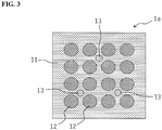
- FIG. 3 shows a wiring board 1a according to another modified example of the first embodiment.
- the alumina protruding parts 13 are arranged on all of areas between diagonally adjacent ones of the connection pads 12 as shown in FIG. 1 .
- the present invention is however not limited to such a configuration.
- the alumina protruding parts 13 are provided at least at three locations in a non-linear arrangement as in the wiring board 1a shown in FIG. 3 .
- a lower surface of the upper-side wiring board 1a is supported by upper ends of the alumina protruding parts 13 of the lower-side wiring board 1a so as to prevent the upper-side wiring board 1a from coming into contact with the connection pads 12 of the lower-side wiring board 1a, and thereby avoid damage to the connection pads 12 of the lower-side wiring board 1a.
- the wiring board 1a is placed on e.g. a stage of component mounting equipment, the wiring board 1a is supported on the stage by contact of the alumina protruding parts 13 with a surface of the stage so as to avoid damage to the connection pads 12 of the wiring board 1a.
- the wiring board 1 is characterized in that the alumina protruding parts 13 are arranged on the areas of the insulating substrate 11 except the areas on which the connection pads 12 are arranged and each has a height greater than that the connection pads 12.
- the connection pads 12 are made unlikely to come into contact with other parts or members so that the surfaces of the connection pads 12 can be protected by the alumina protruding parts 13.
- the arrangement areas of the connection pads 12 would not be narrowed by the arrangement of the alumina protruding parts 13 as the alumina protruding parts 13 are arranged at locations outside of the arrangement areas of the connection pads 12.
- the wiring board 1 therefore provides effective protection for the surfaces of the connection pads 12 without narrowing the intervals between the adjacent connection pads 12.
- each of the alumina protruding parts 13 is arranged between adjacent ones of the connection pads 12 in the first embodiment.
- the alumina protruding parts 13 are located in the vicinities of the connection pads 12 so that the connection pads 12 can be more adequately protected by the alumina protruding parts 13.
- the arrangement of the alumina protruding parts 13 between diagonally adjacent ones of the connection pads 12 makes it easy to ensure the arrangement areas (occupancy areas) of the alumina protruding parts 13 and thereby makes it possible to increase the diameter of the alumina protruding parts 13.
- the alumina protruding parts 13 are circular-column shaped in the first embodiment as shown in FIG. 1 , the shape of the alumina protruding parts 13 is not limited to the circular column shape.
- the alumina protruding parts 13 may have any other shape such as tapered column shape that gradually decreases in diameter toward the upper side (e.g. conical frustum shape, pyramidal frustum shape etc.).
- the second embodiment specifically refers to a wiring board 201.
- FIG. 4 shows a configuration of the wiring board 201.
- the wiring board 201 is shown in plan in the upper part of FIG. 4 .
- the wiring board 201 is shown in cross section along line C-C.
- the wiring board 201 generally includes an insulating substrate 11, a plurality of connection pads 12 (as connection terminals), a plurality of protruding parts 213 (as non-conductive protruding parts) and a plurality of columnar parts 214.
- the insulating substrate 11 and connection pads 12 of the wiring board 201 according to the second embodiment are the same in configuration as those of the wiring board 1 according to the first embodiment.
- the plurality of protruding parts 213 are arranged on areas of the upper main surface of the insulating substrate 11 except areas on which the conductive pads 12 are arranged. In the second embodiment, the plurality of protruding parts 213 are arranged in such a manner that each of the protruding parts 213 is located between diagonally adjacent ones of the two-dimensionally arranged connection pads 12 as shown in the plan view of FIG. 4 .
- each of the protruding parts 213 is made of a non-conductive material.
- the alumina protruding parts 213 are each made of a ceramic material containing alumina (Al 2 O 3 ) as in the first embodiment.
- the protruding parts 213 are thus hereinafter also referred to as "alumina protruding parts 213".
- the material of the protruding parts 213 is not limited to the ceramic material.
- the material of the protruding parts 213 there can be used the same materials as those mentioned above as the material of the protruding parts 13 in the first embodiment.
- the height of the alumina protruding parts 213 is greater than the height of the connection pads 12.
- the height of the alumina protruding part 213 means a distance from the upper surface of the insulating substrate 11 to an uppermost point of the alumina protruding part 213; and the height of the connection pad 12 means a distance from the upper surface of the insulating substrate 11 to an uppermost point of the connection pad 12.
- the height of the alumina protruding parts 213 is greater by a distance h2 than the height of the connection pads 12.
- the plurality of columnar parts 214 are arranged below the alumina protruding parts 213, respectively. More specifically, the columnar parts 214 are embedded in the insulating substrate 11 at positions corresponding to the alumina protruding parts 213, with upper end portions of the columnar parts 214 protruding from the upper surface of the insulating substrate 11 and being covered by the alumina protruding parts 213, as shown in the cross-sectional view of FIG. 4 .
- Each of the columnar parts 214 is made of a material having a lower thermal shrinkage rate than that of the insulating substrate 11.
- the insulating substrate 11 contains a ceramic material as a predominant component as in the first embodiment; whereas the columnar parts 214 contain as a predominant component a metal material lower in thermal shrinkage rate than the ceramic material.
- the term "predominant component” as used herein means a component whose content (in terms of wt%) is the highest among all components of the insulating substrate 11 or the columnar part 214.
- the metal material are copper (Cu), silver (Ag), palladium (Pd), gold (Au), platinum (Pt), tungsten (W), molybdenum (Mo) and manganese (Mn).
- the columnar parts 214 may be made of the same material as the connection pads 12.
- the columnar parts 214 are caused to partially protrude from the surface of the insulating substrate 11 under the application of heat by firing during the manufacturing process of the wiring board 211 due to a difference in thermal shrinkage rate between the insulating substrate 11 and the columnar parts 214.
- the alumina protruding parts 213 located above the columnar parts 214 protrude to a greater height. As a result, a sufficient height of the alumina protruding parts 213 is ensured.
- FIGS. 5A to 5C show the respective steps of the manufacturing process of the wiring board 201.
- the columnar parts 214 are arranged in the insulating substrate 11 at predetermined positions as shown in FIG. 5A .
- the predetermined positions correspond to the areas of the insulating substrate 11 on which the connection pads 12 are to be arranged in the subsequent step.
- the diameter D5 of the columnar parts 214 is set smaller than the diameter D6 of the alumina protruding parts 213 formed in the later step.
- the upper surfaces of the columnar parts 214 are in flush with the upper surface of the insulating substrate 11 in the second embodiment.
- connection pads 12 are formed and arranged on the predetermined areas of the insulating substrate 11.
- the connection pads 12 can be formed by a conventionally known printing technique such as screen printing.
- a non-conductive material 213a as the raw material of the alumina protruding parts 213 is deposited on the areas of the insulating substrate 11, except the areas on which the connection pads 12 are arranged, so as to overlap and cover the columnar parts 214 as shown in FIG. 5B .
- the ceramic material containing alumina Al 2 O 3
- the non-conductive material 213a can be deposited by a conventionally known printing technique such as screen printing.
- the insulating substrate 11 in which the columnar parts 214 have been arranged and on which the non-conductive material 213a has been deposited is subjected to firing.
- the non-conductive material 213a is pushed upward and thereby formed into protrusions.
- the thus-provided alumina protruding parts 213 have a circular column shape or a substantially conical frustum shape that decreases in diameter toward the upper side.
- the alumina protruding parts 213 are formed to protrude to a greater height than the connection pads 12 with the aid of a difference in thermal shrinkage rate between the material (e.g. ceramic material) of the insulating substrate 11 and the material (e.g. metal material) of the columnar parts 214 as mentioned above.
- the difference h2 between the height of the alumina protruding parts 213 and the connection pads 12 in the second embodiment is hence set larger than the difference h1 between the height of the alumina protruding parts 12 and the connection pads 12 in the first embodiment.
- connection pads 12 in the second embodiment As the difference h2 between the height of the alumina protruding parts 213 and the connection pads 12 in the second embodiment is set larger, it is more unlikely that the connection pads 12 will come into contact with other parts or members even under the influence of warpage or deformation of the wiring board 201 itself.
- Each of the columnar parts 214 arranged in the insulating substrate 11 may be in multilayer form.
- the height of protrusion of the columnar part 214 from the surface of the insulating substrate 11 after the application of heat is made larger by setting the diameter D5 of the lower layer of the multilayer columnar part 214 larger.
- the height of protrusion of the columnar part 214 from the surface of the insulating substrate 11 after the application of heat is also made larger by using a metal material with a lower thermal shrinkage rate (e.g. a metal material lower in thermal shrinkage rate than the metal material of the connection pads 12) as the material of the columnar part 214.
- the second columnar parts 214 serve as vias for connection of connection terminals to wirings inside the insulating substrate 11.
- Each of the second columnar parts is made of a conductive material such as metal material.
- the third embodiment specifically refers to a wiring board 301.
- the wiring board 301 according to the third embodiment is structurally the same as the wiring boards 1 and 201 according to the first and second embodiments, except for the configuration of non-conductive protruding parts.
- FIGS. 6, 7 and 8A to 8D show configuration examples of the non-conductive protruding parts.
- the non-conductive protruding parts provided are alumina protruding parts 313a having a square shape when viewed in plan.
- the diameter ⁇ of the connection pads 12 is set to e.g. 0.75 mm; and the length L of one side of the square-shaped alumina protruding parts 313a is set to e.g. 0.30 mm.
- the non-conductive protruding parts provided are alumina protruding parts 313b having an acute-angled square shape in plan view.
- the areas of arrangement of the alumina protruding parts 313b is ensured easily and reliably even when the intervals between the connection pads 12 is made narrower.
- alumina protruding parts 313c oval-shaped alumina protruding parts 313c as shown in FIG. 8A
- triangular-shaped alumina protruding parts 313d as shown in FIG. 8B
- cross-shaped alumina protruding parts 313e as shown in FIG. 8C
- FIG. 8D it is feasible to provide square-shaped alumina protruding parts 313f in a different orientation from that of the square-shaped alumina protruding parts 313a shown in FIG. 6 .
- the alumina protruding parts 313a, 313f may alternatively be rectangular in shape.
Landscapes
- Engineering & Computer Science (AREA)
- Microelectronics & Electronic Packaging (AREA)
- Manufacturing & Machinery (AREA)
- Chemical & Material Sciences (AREA)
- Ceramic Engineering (AREA)
- Inorganic Chemistry (AREA)
- Production Of Multi-Layered Print Wiring Board (AREA)
- Structure Of Printed Boards (AREA)
- Printing Elements For Providing Electric Connections Between Printed Circuits (AREA)
Abstract
Description
- The present invention relates to a wiring board with a plurality of connection terminals and a manufacturing method thereof.
- There is known a wiring board for mounting thereon an electronic component e.g. semiconductor element, which includes: an insulating substrate made of a non-conductive material such as a ceramic material, resin material or glass material; and a plurality of external connection terminals (also called "connection pads") made of a conductive material such as a metal material on the insulating substrate.
- Japanese Laid-Open Patent Publication No.
2015-225893 - In the above-disclosed wiring board, the coating layer of non-conductive material is applied to the outer peripheral portions of the pad conductors. In this way, there are cases where the coating layer is formed to overlap and cover parts of the connection pads for the purpose of preventing damage to surfaces of the connection pads and entry of foreign matter between the connection pads. Such a layer structure is called an "overcoat structure". It is conceivable to form the overcoat structure by arranging the connection pads in a predetermined pattern on the insulating layer, and then, laminating the coating layer of non-conductive material (such as alumina) to cover from the insulating substrate to outer peripheral portions of the connection pads, whereby portions of the connection pads exposed from the coating layer serve as connection terminals for connection to other connection members such as solder balls.
- In the overcoat structure, the actual diameter of the connection pads located under the coating layer is larger than the diameter of the exposed portions of the connection pads serving as the connection terminals. When it is demanded to narrow the intervals between the adjacent connection pads for high definition and miniaturization of the wiring board, the connection pads have to be located very close to each other under the coating layer.
- However, the narrowing of the intervals between the adjacent connection pads raises difficulties in manufacturing process. The narrowing of the intervals between the adjacent connection pads also raises a high possibility of short circuit between the adjacent connection pads, which results in an increase of defective product rate.
- In view of the foregoing, it is a main advantage of the present invention to provide a wiring board capable of protecting surfaces of connection terminals without narrowing the intervals between the adjacent connection terminals and to provide a method for manufacturing such a wiring board.
- According to one aspect of the present invention, there is provided a wiring board, comprising: an insulating substrate; a plurality of connection terminals arranged on the insulating substrate; and a plurality of non-conductive protruding parts respectively arranged on areas of the insulating substrate except areas on which the plurality of connection terminals are arranged, the non-conductive protruding parts having a height greater than that of the connection terminals.
- According to another aspect of the present invention, there is provided a manufacturing method of a wiring board, comprising: providing an insulating substrate in which a plurality of columnar parts are arranged, the columnar parts being made of a material having a lower thermal shrinkage rate than that of the insulating substrate; arranging connection terminals on areas of the insulating substrate except areas corresponding in position to the columnar parts; depositing a non-conductive material over the columnar parts on the insulating substrate; and heating or firing the insulating substrate on which the non-conductive material has been deposited, so as to allow the columnar parts to partially protrude from the insulating substrate due to a difference in thermal shrinkage rate between the insulating substrate and the columnar parts and thereby form protruding parts containing the non-conductive material.
- The other objects and features of the present invention will also become understood from the following description.
-
-
FIG. 1 is a plan view and cross-sectional view of a wiring board according to a first embodiment of the present invention. -
FIG. 2 is a plan view and cross-sectional view of a wiring board according to a modified example of the first embodiment. -
FIG. 3 is a plan view of a wiring board according to another modified example of the first embodiment. -
FIG. 4 is a plan view and cross-sectional view of a wiring board according to a second embodiment of the present invention. -
FIGS. 5A to 5C are schematic views of a process for manufacturing of the wiring board according to the second embodiment of the present invention. -
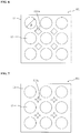
FIGS. 6 and 7 are schematic plan views of examples of a wiring board according to a third embodiment of the present invention. -
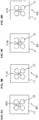
FIGS. 8A to 8D are schematic plan views of other examples of the wiring board according to the third embodiment of the present invention. -
FIG. 9 is a plan view and cross-sectional view of a conventional wiring board. - Hereinafter, exemplary embodiments of the present invention will be described in detail below with reference to the drawings. In the following description, like parts and portions are designated by like reference numerals. These like parts and portions have the same names and functions. Thus, repeated explanation of the like parts and portions will be omitted herefrom. Further, the terms "upper", "lower", "under", "below", "above" etc. are used to describe relative locations of parts and portions as shown in the drawings.
- The first embodiment specifically refers to a
wiring board 1 usable for various electronic devices. -
FIG. 1 shows a configuration of thewiring board 1. Thewiring board 1 is shown in plan in the upper part ofFIG. 1 . In the lower part ofFIG. 1 , thewiring board 1 is shown in cross section along line A-A. - As shown in
FIG. 1 , thewiring board 1 generally includes aninsulating substrate 11, a plurality of connection pads 12 (as connection terminals) and a plurality of protruding parts 13 (as non-conductive protruding parts). - The
insulating substrate 11 is made of an insulating material. In the first embodiment, theinsulating substrate 11 contains a ceramic material as a predominant component. The term "predominant component" as used herein means a component whose content (in terms of wt%) is the highest among all components of theinsulating substrate 11. Examples of the insulating material are a ceramic material containing alumina (Al2O3), a glass-ceramics composite material such as LTCC (low temperature co-fired ceramics) and the like. Theinsulating substrate 11 may have a laminated structure formed by laminating a plurality of insulating material layers (such as ceramic green sheets). - The plurality of
connection pads 12 are arranged on an upper main surface of theinsulating substrate 11. In the first embodiment, theconnection pads 12 are aligned at substantially equal intervals in lengthwise and widthwise directions of theinsulating substrate 11, that is, arranged two-dimensionally in a grid pattern. Thus, theconductive pads 12 are also called "BGA (ball grid array) pads", "LGA (land grid array) pads", "PGA (pin grid array) pads" etc. - Each of the
conductive pads 12 is made of a conductive material. Examples of the conductive material are metal materials such as copper (Cu), silver (Ag), palladium (Pd), gold (Au), platinum (Pt), tungsten (W), molybdenum (Mo), nickel (Ni), manganese (Mn) and alloys thereof. These metal materials can be applied to theinsulating substrate 11 by metallization, plating, deposition etc. Theconductive pads 12 may contain an inorganic material such as glass or alumina in addition to the metal material. - In the case where the
connection pads 12 are provided as metallization layers of tungsten (W), molybdenum (Mo) etc., it is feasible to form theconnection pads 12 by e.g. kneading a powder of the aforementioned metal with an organic solvent and a binder, applying the resulting metal paste in a predetermined pattern onto a ceramic green sheet as the material of theinsulating substrate 11 and then co-firing the ceramic green sheet and the applied metal paste. The application of the metal paste can be done by a conventionally known printing technique such as screen printing. - The plurality of protruding
parts 13 are arranged on areas of the upper main surface of theinsulating substrate 11 except areas on which theconductive pads 12 are arranged. In the first embodiment, the plurality of protrudingparts 13 are arranged in such a manner that each of theprotruding parts 13 is located between diagonally adjacent ones of the two-dimensionally arrangedconnection pads 12 as shown in the plan view ofFIG. 1 . - Each of the
protruding parts 13 is made of a non-conductive material. In the first embodiment, theprotruding parts 13 are each made of a ceramic material containing alumina (Al2O3). The protrudingparts 13 are thus hereinafter also referred to as "alumina protruding parts 13". In the present invention, however, the material of theprotruding parts 13 is not limited to the ceramic material. The protrudingparts 13 may alternatively be made of any other non-conductive material such as resin material e.g. solder resist, glass-ceramics composite material e.g. LTCC, glass material, or the like. - As shown in the cross-sectional view of
FIG. 1 , the height of thealumina protruding parts 13 is greater than the height of theconnection pads 12. Herein, the height of thealumina protruding part 13 means a distance from the upper surface of the insulatingsubstrate 11 to an uppermost point of thealumina protruding part 13; and the height of theconnection pad 12 means a distance from the upper surface of the insulatingsubstrate 11 to an uppermost point of theconnection pad 12. Accordingly, the distance from the upper surface of the insulatingsubstrate 11 to the uppermost points of thealumina protruding parts 13 is greater than the distance from the upper surface of the insulatingsubstrate 11 to the uppermost points of theconnection pads 12. In the first embodiment shown inFIG. 1 , the height of thealumina protruding parts 13 is greater by a distance h1 than the height of theconnection pads 12. - In such a configuration, the
alumina protruding parts 13 of greater height are arranged in the vicinities of theconnection pads 12. Theconnection pads 12 are thus made unlikely to come into contact with other parts or members so that surfaces of theconnection pads 12 can be protected by thealumina protruding parts 13. - Further, each of the
alumina protruding parts 13 is formed in a vertically elongated column shape and is located between adjacent ones of theconnection pads 12 at a distance away from theconnection pads 12 so as not to interfere with theconnection pads 12 in the first embodiment. This ensures the areas of arrangement of thealumina protruding parts 13 at locations outside of (different from) the areas of arrangement of theconnection pads 12 while maintaining the intervals between theconnection pads 12. - The correlation between the arrangement areas of the
alumina protruding parts 13 and the intervals between thecorrection pads 12 will be explained in more detail below with reference toFIGS. 1 ,2 and9 . -
FIG. 2 shows awiring board 101 according to a modified example of the first embodiment. Thewiring board 101 is shown in plan in the upper part ofFIG. 2 . In the lower part ofFIG. 2 , thewiring board 101 is shown in cross section along line B-B. -
FIG. 9 shows a configuration of theconventional wiring board 901. Thewiring board 901 is shown in plan in the upper part ofFIG. 9 . In the lower part ofFIG. 9 , thewiring board 901 is shown in cross section along line D-D. - As shown in
FIG. 9 , theconventional wiring board 901 hasconnection pads 912 arranged on the insulatingsubstrate 11, with acoating layer 913 of non-conductive material covering from the insulatingsubstrate 11 to outer peripheral portions of theconnection pads 912. Thecoating layer 913 is formed to overlap and cover parts of the connection pads 912 (see the cross-sectional view ofFIG. 9 ) for the purpose of preventing damage to surfaces of theconnection pads 912 and entry of foreign matter between theconnection pads 912. Thecoating layer 913 is thus also called "overcoat layer". In the conventional example shown inFIG. 9 , the overlap between thecoating layer 913 and the outer peripheral portion of theconnection pad 912 is provided with a width d3 (e.g. greater than or equal to 0.05 mm and smaller than or equal to 0.15 mm). - The
coating layer 913 is formed by e.g. arranging theconnection pads 912 in a predetermined pattern on the insulatingsubstrate 11, and then, laminating the non-conductive material (such as alumina) on the insulating substrate to cover the outer peripheral portions of theconnection pads 912. Then, portions of theconnection pads 912 exposed from thecoating layer 913 respectively serve as connection terminals for connection to other connection members such as solder balls. - In the
conventional wiring board 901, the actual diameter d1 (e.g. 0.95 mm) of theconnection pads 912 located under thecoating layer 913 is larger than the diameter d2 (e.g. 0.75 mm) of the exposed portions of theconnection pads 912 serving as the connection terminals. When it is demanded to narrow the apparent intervals d4 (e.g. 0.25 mm) between theadjacent connection pads 912 for high definition and miniaturization of thewiring board 901, theconnection pads 912 have to be located very close to each other under thecoating layer 913. In the conventional example shown inFIG. 9 , the actual intervals between theadjacent connection pads 912 under thecoating layer 913 are narrowed to a very small value d5 (e.g. 0.05 mm). - However, the narrowing of the actual intervals d5 between the
adjacent connection pads 912 raises difficulties in manufacturing process. The narrowing of the actual intervals d5 between theadjacent connection pads 912 also raises a high possibility of short circuit between theadjacent connection pads 912, which results in an increase of defective product rate. Herein, the interval between the adjacent connection pads means a distance from an edge of one of two adjacent connection pads to an edge of the other of the two adjacent connection pads. - As in the
wiring board 101 shown inFIG. 2 , it is hence desirable to arrange aprotection layer 113 of alumina etc. andconnection pads 12 on the insulatingsubstrate 11 with no clearance created therebetween. In the modified example shown inFIG. 2 , the height of thealumina protection layer 113 is greater by a distance h1 than the height of theconnection pads 12 as in the first embodiment shown inFIG. 1 . Thus, thealumina protection layer 113 serve as non-conductive protruding parts to protect surfaces of theconnection pads 12 in thewiring board 101. - In the case where, in the
wiring board 101, the diameter D1 of theconnection pads 12 is 0.75 mm; and the center-to-center distance D2 of theadjacent connection pads 12 is 1.00 mm, the actual interval D3 between theadjacent connection pads 12 is 0.25 mm. In this way, a certain amount of interval is ensured between theadjacent connection pads 12 so that the possibility of short circuit between theadjacent connection pads 12 is reduced in the modification example. - In the modified example shown in
FIG. 2 , however, it is required to perform patterning with very high positional accuracy for the formation of theconnection pads 12 and thealumina protection layer 113. Such very high accuracy patterning is difficult to perform by a conventionally known printing technique. - In the first embodiment, on the other hand, each of the
alumina protruding parts 13 is located between adjacent ones of theconnection pads 12 at a distance slightly away from theseadjacent connection pads 12 as mentioned above. In the case where the diameter D1 and center-to-center distance D2 of theconnection pads 12 of thewiring board 1 are set to the same as those of thewiring board 101, thealumina protruding parts 13 can be located at some space away from theadjacent connection pads 12. Furthermore, thealumina protruding parts 13 can be formed with relatively easily realizable dimensions (e.g. diameter D4 = 0.35 mm). -
FIG. 3 shows a wiring board 1a according to another modified example of the first embodiment. - In the first embodiment, the
alumina protruding parts 13 are arranged on all of areas between diagonally adjacent ones of theconnection pads 12 as shown inFIG. 1 . The present invention is however not limited to such a configuration. - It suffices that the
alumina protruding parts 13 are provided at least at three locations in a non-linear arrangement as in the wiring board 1a shown inFIG. 3 . In this configuration, when a plurality of the wiring board 1a are stacked together, a lower surface of the upper-side wiring board 1a is supported by upper ends of thealumina protruding parts 13 of the lower-side wiring board 1a so as to prevent the upper-side wiring board 1a from coming into contact with theconnection pads 12 of the lower-side wiring board 1a, and thereby avoid damage to theconnection pads 12 of the lower-side wiring board 1a. When the wiring board 1a is placed on e.g. a stage of component mounting equipment, the wiring board 1a is supported on the stage by contact of thealumina protruding parts 13 with a surface of the stage so as to avoid damage to theconnection pads 12 of the wiring board 1a. - As mentioned above, the
wiring board 1 according to the first embodiment is characterized in that thealumina protruding parts 13 are arranged on the areas of the insulatingsubstrate 11 except the areas on which theconnection pads 12 are arranged and each has a height greater than that theconnection pads 12. As thealumina protruding parts 13 of greater height than theconnection pads 12 are arranged, theconnection pads 12 are made unlikely to come into contact with other parts or members so that the surfaces of theconnection pads 12 can be protected by thealumina protruding parts 13. Further, the arrangement areas of theconnection pads 12 would not be narrowed by the arrangement of thealumina protruding parts 13 as thealumina protruding parts 13 are arranged at locations outside of the arrangement areas of theconnection pads 12. Thewiring board 1 therefore provides effective protection for the surfaces of theconnection pads 12 without narrowing the intervals between theadjacent connection pads 12. - In particular, each of the
alumina protruding parts 13 is arranged between adjacent ones of theconnection pads 12 in the first embodiment. In such an arrangement, thealumina protruding parts 13 are located in the vicinities of theconnection pads 12 so that theconnection pads 12 can be more adequately protected by thealumina protruding parts 13. Moreover, the arrangement of thealumina protruding parts 13 between diagonally adjacent ones of theconnection pads 12 makes it easy to ensure the arrangement areas (occupancy areas) of thealumina protruding parts 13 and thereby makes it possible to increase the diameter of thealumina protruding parts 13. - Although the
alumina protruding parts 13 are circular-column shaped in the first embodiment as shown inFIG. 1 , the shape of thealumina protruding parts 13 is not limited to the circular column shape. Thealumina protruding parts 13 may have any other shape such as tapered column shape that gradually decreases in diameter toward the upper side (e.g. conical frustum shape, pyramidal frustum shape etc.). - The second embodiment specifically refers to a
wiring board 201. -
FIG. 4 shows a configuration of thewiring board 201. Thewiring board 201 is shown in plan in the upper part ofFIG. 4 . In the lower part ofFIG. 4 , thewiring board 201 is shown in cross section along line C-C. - As shown in
FIG. 4 , thewiring board 201 generally includes an insulatingsubstrate 11, a plurality of connection pads 12 (as connection terminals), a plurality of protruding parts 213 (as non-conductive protruding parts) and a plurality ofcolumnar parts 214. The insulatingsubstrate 11 andconnection pads 12 of thewiring board 201 according to the second embodiment are the same in configuration as those of thewiring board 1 according to the first embodiment. - The plurality of protruding
parts 213 are arranged on areas of the upper main surface of the insulatingsubstrate 11 except areas on which theconductive pads 12 are arranged. In the second embodiment, the plurality of protrudingparts 213 are arranged in such a manner that each of the protrudingparts 213 is located between diagonally adjacent ones of the two-dimensionally arrangedconnection pads 12 as shown in the plan view ofFIG. 4 . - Each of the protruding
parts 213 is made of a non-conductive material. In the second embodiment, thealumina protruding parts 213 are each made of a ceramic material containing alumina (Al2O3) as in the first embodiment. The protrudingparts 213 are thus hereinafter also referred to as "alumina protruding parts 213". In the present invention, however, the material of the protrudingparts 213 is not limited to the ceramic material. Regarding the material of the protrudingparts 213, there can be used the same materials as those mentioned above as the material of the protrudingparts 13 in the first embodiment. - As shown in the cross-sectional view of
FIG. 4 , the height of thealumina protruding parts 213 is greater than the height of theconnection pads 12. Herein, the height of thealumina protruding part 213 means a distance from the upper surface of the insulatingsubstrate 11 to an uppermost point of thealumina protruding part 213; and the height of theconnection pad 12 means a distance from the upper surface of the insulatingsubstrate 11 to an uppermost point of theconnection pad 12. In the second embodiment shown inFIG. 4 , the height of thealumina protruding parts 213 is greater by a distance h2 than the height of theconnection pads 12. - The plurality of
columnar parts 214 are arranged below thealumina protruding parts 213, respectively. More specifically, thecolumnar parts 214 are embedded in the insulatingsubstrate 11 at positions corresponding to thealumina protruding parts 213, with upper end portions of thecolumnar parts 214 protruding from the upper surface of the insulatingsubstrate 11 and being covered by thealumina protruding parts 213, as shown in the cross-sectional view ofFIG. 4 . - Each of the
columnar parts 214 is made of a material having a lower thermal shrinkage rate than that of the insulatingsubstrate 11. In the second embodiment, the insulatingsubstrate 11 contains a ceramic material as a predominant component as in the first embodiment; whereas thecolumnar parts 214 contain as a predominant component a metal material lower in thermal shrinkage rate than the ceramic material. The term "predominant component" as used herein means a component whose content (in terms of wt%) is the highest among all components of the insulatingsubstrate 11 or thecolumnar part 214. Examples of the metal material are copper (Cu), silver (Ag), palladium (Pd), gold (Au), platinum (Pt), tungsten (W), molybdenum (Mo) and manganese (Mn). Thecolumnar parts 214 may be made of the same material as theconnection pads 12. - As will be explained in detail below, the
columnar parts 214 are caused to partially protrude from the surface of the insulatingsubstrate 11 under the application of heat by firing during the manufacturing process of the wiring board 211 due to a difference in thermal shrinkage rate between the insulatingsubstrate 11 and thecolumnar parts 214. With the protrusion of thecolumnar parts 214, thealumina protruding parts 213 located above thecolumnar parts 214 protrude to a greater height. As a result, a sufficient height of thealumina protruding parts 213 is ensured. -
FIGS. 5A to 5C show the respective steps of the manufacturing process of thewiring board 201. - First, the
columnar parts 214 are arranged in the insulatingsubstrate 11 at predetermined positions as shown inFIG. 5A . The predetermined positions correspond to the areas of the insulatingsubstrate 11 on which theconnection pads 12 are to be arranged in the subsequent step. At this time, the diameter D5 of thecolumnar parts 214 is set smaller than the diameter D6 of thealumina protruding parts 213 formed in the later step. Further, the upper surfaces of thecolumnar parts 214 are in flush with the upper surface of the insulatingsubstrate 11 in the second embodiment. - Next, the
connection pads 12 are formed and arranged on the predetermined areas of the insulatingsubstrate 11. As mentioned above, theconnection pads 12 can be formed by a conventionally known printing technique such as screen printing. - Subsequently, a
non-conductive material 213a as the raw material of thealumina protruding parts 213 is deposited on the areas of the insulatingsubstrate 11, except the areas on which theconnection pads 12 are arranged, so as to overlap and cover thecolumnar parts 214 as shown inFIG. 5B . In the second embodiment, the ceramic material containing alumina (Al2O3) is used as thenon-conductive material 213a as mentioned above. Thenon-conductive material 213a can be deposited by a conventionally known printing technique such as screen printing. - After that, the insulating
substrate 11 in which thecolumnar parts 214 have been arranged and on which thenon-conductive material 213a has been deposited is subjected to firing. The insulatingsubstrate 11, thecolumnar parts 214 and thenon-conductive material 213a undergo shrinkage under the application of heat by firing. Since the thermal shrinkage rate of thecolumnar part 214 is lower than the thermal shrinkage rate of the insulatingsubstrate 11, the amount of shrinkage of the insulatingsubstrate 11 is larger than the amount of shrinkage of thecolumnar part 214. Consequently, there occurs a change in configuration such that thecolumnar parts 214 partially protrude from the thermally shrunk insulatingsubstrate 11 as shown by arrows inFIG. 5C . With such a configuration change, thenon-conductive material 213a is pushed upward and thereby formed into protrusions. There are thus provided thealumina protruding parts 213. The thus-providedalumina protruding parts 213 have a circular column shape or a substantially conical frustum shape that decreases in diameter toward the upper side. - In the manufacturing process of the
wiring board 201, thealumina protruding parts 213 are formed to protrude to a greater height than theconnection pads 12 with the aid of a difference in thermal shrinkage rate between the material (e.g. ceramic material) of the insulatingsubstrate 11 and the material (e.g. metal material) of thecolumnar parts 214 as mentioned above. The difference h2 between the height of thealumina protruding parts 213 and theconnection pads 12 in the second embodiment is hence set larger than the difference h1 between the height of thealumina protruding parts 12 and theconnection pads 12 in the first embodiment. As the difference h2 between the height of thealumina protruding parts 213 and theconnection pads 12 in the second embodiment is set larger, it is more unlikely that theconnection pads 12 will come into contact with other parts or members even under the influence of warpage or deformation of thewiring board 201 itself. - Each of the
columnar parts 214 arranged in the insulatingsubstrate 11 may be in multilayer form. In this case, the height of protrusion of thecolumnar part 214 from the surface of the insulatingsubstrate 11 after the application of heat is made larger by setting the diameter D5 of the lower layer of the multilayercolumnar part 214 larger. The height of protrusion of thecolumnar part 214 from the surface of the insulatingsubstrate 11 after the application of heat is also made larger by using a metal material with a lower thermal shrinkage rate (e.g. a metal material lower in thermal shrinkage rate than the metal material of the connection pads 12) as the material of thecolumnar part 214. - In a modified example of the second embodiment, not only the
columnar parts 214 but also additional (second) columnar parts may be provided inside the insulatingsubstrate 11. For example, the second columnar parts serve as vias for connection of connection terminals to wirings inside the insulatingsubstrate 11. Each of the second columnar parts is made of a conductive material such as metal material. In the case where the second columnar parts are provided, it is preferable to select and use as the material of the columnar parts 214 a material having a lower thermal shrinkage rate than that of the second columnar parts. By the selection and use of such materials, the height of protrusion of thecolumnar parts 214 from the surface of the insulatingsubstrate 11 after the firing is made larger than that of the second columnar parts. - The third embodiment specifically refers to a
wiring board 301. Thewiring board 301 according to the third embodiment is structurally the same as thewiring boards -
FIGS. 6, 7 and8A to 8D show configuration examples of the non-conductive protruding parts. - In the example shown in
FIG. 6 , the non-conductive protruding parts provided are alumina protruding parts 313a having a square shape when viewed in plan. For instance, the diameter φ of theconnection pads 12 is set to e.g. 0.75 mm; and the length L of one side of the square-shaped alumina protruding parts 313a is set to e.g. 0.30 mm. - In the example shown in
FIG. 7 , the non-conductive protruding parts provided arealumina protruding parts 313b having an acute-angled square shape in plan view. In this case, the areas of arrangement of thealumina protruding parts 313b is ensured easily and reliably even when the intervals between theconnection pads 12 is made narrower. - It is alternatively feasible to provide, as the non-conductive protruding parts, oval-shaped
alumina protruding parts 313c as shown inFIG. 8A , triangular-shapedalumina protruding parts 313d as shown inFIG. 8B , or cross-shapedalumina protruding parts 313e as shown inFIG. 8C . As shown inFIG. 8D , it is feasible to provide square-shapedalumina protruding parts 313f in a different orientation from that of the square-shaped alumina protruding parts 313a shown inFIG. 6 . Thealumina protruding parts 313a, 313f may alternatively be rectangular in shape. - Although the present invention has been described above with reference to the specific embodiments and examples, the above-described embodiments and examples are intended to facilitate understanding of the present invention and are not intended to limit the present invention thereto. Various changes and modifications can be made to the above embodiments and examples without departing from the scope of the present invention. The present invention includes equivalents thereof and any combinations of the features of the above embodiments and examples.
Claims (6)
- A wiring board (1; 1a; 101; 201; 301), comprising:an insulating substrate (11);a plurality of connection terminals (12) arranged on the insulating substrate (11); anda plurality of non-conductive protruding parts (13; 113; 213; 313a; 313b; 313c; 313d; 313e; 313f) respectively arranged on areas of the insulating substrate (11) except areas on which the plurality of connection terminals (12) are arranged,the non-conductive protruding parts (13; 113; 213; 313a; 313b; 313c; 313d; 313e; 313f) having a height greater than that of the connection terminals (12).
- The wiring board (1; 1a; 101; 201; 301) according to claim 1,
wherein each of the plurality of non-conductive protruding parts (13; 113; 213; 313a; 313b; 313c; 313d; 313e; 313f) is located between adjacent ones of the plurality of connection terminals (12). - The wiring board (1; 1a; 101; 201; 301) according to claim 1 or 2,
wherein the plurality of non-conductive protruding parts (13; 113; 213; 313a; 313b; 313c; 313d; 313e; 313f) are at least three non-conductive protruding parts and are in a non-linear arrangement. - The wiring board (201) according to any one of claims 1 to 3, further comprising columnar parts (214) respectively arranged under the non-conductive protruding parts (213) and made of a material having a lower thermal shrinkage rate than that of the insulating substrate (11).
- The wiring board (201) according to claim 4,
wherein the insulating substrate (11) contains a ceramic material as a predominant component, and
wherein the columnar parts (214) contain a metal material as a predominant component. - A manufacturing method of a wiring board (201), comprising:providing an insulating substrate (11) in which a plurality of columnar parts (214) are arranged, the columnar parts (214) being made of a material having a lower thermal shrinkage rate than that of the insulating substrate (11);arranging connection terminals (12) on areas of the insulating substrate (11) except areas corresponding in position to the columnar parts (214);depositing a non-conductive material (213a) over the columnar parts (214) on the insulating substrate (11); andheating or firing the insulating substrate (11) on which the non-conductive material (213a) has been deposited, so as to allow the columnar parts (214) to partially protrude from the insulating substrate (11) due to a difference in thermal shrinkage rate between the insulating substrate (11) and the columnar parts (214) and thereby form protruding parts (213) containing the non-conductive material (213a).
Applications Claiming Priority (1)
| Application Number | Priority Date | Filing Date | Title |
|---|---|---|---|
| JP2019091823A JP7142604B2 (en) | 2019-05-15 | 2019-05-15 | Wiring board and its manufacturing method |
Publications (2)
| Publication Number | Publication Date |
|---|---|
| EP3740048A1 true EP3740048A1 (en) | 2020-11-18 |
| EP3740048B1 EP3740048B1 (en) | 2025-08-13 |
Family
ID=70058277
Family Applications (1)
| Application Number | Title | Priority Date | Filing Date |
|---|---|---|---|
| EP20166816.7A Active EP3740048B1 (en) | 2019-05-15 | 2020-03-30 | Wiring board and manufacturing method thereof |
Country Status (4)
| Country | Link |
|---|---|
| US (1) | US10849224B1 (en) |
| EP (1) | EP3740048B1 (en) |
| JP (1) | JP7142604B2 (en) |
| CN (1) | CN111952269B (en) |
Families Citing this family (1)
| Publication number | Priority date | Publication date | Assignee | Title |
|---|---|---|---|---|
| US12284769B2 (en) * | 2019-03-27 | 2025-04-22 | BorgWarner US Technologies LLC | Conformal coating blockage by surface-mount technology solder features |
Citations (6)
| Publication number | Priority date | Publication date | Assignee | Title |
|---|---|---|---|---|
| US20080202804A1 (en) * | 2007-02-26 | 2008-08-28 | Yasuhiro Fakutomi | Printed circuit board and method of producing the same |
| EP2784807A1 (en) * | 2012-11-07 | 2014-10-01 | NGK Spark Plug Co., Ltd. | Circuit board and method for producing same |
| WO2014199890A1 (en) * | 2013-06-14 | 2014-12-18 | 三菱製紙株式会社 | Method for manufacturing wiring board |
| JP2015225893A (en) | 2014-05-26 | 2015-12-14 | 京セラ株式会社 | Wiring board and electronic device |
| US20160007459A1 (en) * | 2014-07-04 | 2016-01-07 | Young-ja KIM | Printed circuit board and semiconductor package using the same |
| JP2016072398A (en) * | 2014-09-29 | 2016-05-09 | 日本特殊陶業株式会社 | Wiring board |
Family Cites Families (12)
| Publication number | Priority date | Publication date | Assignee | Title |
|---|---|---|---|---|
| JP3152834B2 (en) * | 1993-06-24 | 2001-04-03 | 株式会社東芝 | Electronic circuit device |
| JPH11111766A (en) * | 1997-09-30 | 1999-04-23 | Kyocera Corp | Wiring board and method of manufacturing the same |
| US5969461A (en) * | 1998-04-08 | 1999-10-19 | Cts Corporation | Surface acoustic wave device package and method |
| JPH11298142A (en) * | 1998-04-09 | 1999-10-29 | Nec Corp | Mounting structure and mounting method of multilayer ceramic substrate |
| JP5017930B2 (en) * | 2006-06-01 | 2012-09-05 | 富士通株式会社 | Semiconductor device, method for manufacturing solder bump connecting substrate, and method for manufacturing semiconductor device |
| JP2011142185A (en) * | 2010-01-06 | 2011-07-21 | Renesas Electronics Corp | Semiconductor device |
| JP2013149948A (en) * | 2011-12-20 | 2013-08-01 | Ngk Spark Plug Co Ltd | Wiring board and manufacturing method of the same |
| US9497861B2 (en) * | 2012-12-06 | 2016-11-15 | Taiwan Semiconductor Manufacturing Company, Ltd. | Methods and apparatus for package with interposers |
| JP5991915B2 (en) * | 2012-12-27 | 2016-09-14 | ルネサスエレクトロニクス株式会社 | Manufacturing method of semiconductor device |
| JP5799973B2 (en) * | 2013-04-15 | 2015-10-28 | 株式会社村田製作所 | Ceramic multilayer wiring board and module including the same |
| CN104793026B (en) * | 2014-01-20 | 2018-09-28 | 旺矽科技股份有限公司 | Supporting structure applied to probe testing device and manufacturing method thereof |
| US20190206822A1 (en) * | 2017-12-30 | 2019-07-04 | Intel Corporation | Missing bump prevention from galvanic corrosion by copper bump sidewall protection |
-
2019
- 2019-05-15 JP JP2019091823A patent/JP7142604B2/en active Active
-
2020
- 2020-03-04 US US16/808,597 patent/US10849224B1/en active Active
- 2020-03-30 EP EP20166816.7A patent/EP3740048B1/en active Active
- 2020-04-17 CN CN202010305466.8A patent/CN111952269B/en not_active Expired - Fee Related
Patent Citations (6)
| Publication number | Priority date | Publication date | Assignee | Title |
|---|---|---|---|---|
| US20080202804A1 (en) * | 2007-02-26 | 2008-08-28 | Yasuhiro Fakutomi | Printed circuit board and method of producing the same |
| EP2784807A1 (en) * | 2012-11-07 | 2014-10-01 | NGK Spark Plug Co., Ltd. | Circuit board and method for producing same |
| WO2014199890A1 (en) * | 2013-06-14 | 2014-12-18 | 三菱製紙株式会社 | Method for manufacturing wiring board |
| JP2015225893A (en) | 2014-05-26 | 2015-12-14 | 京セラ株式会社 | Wiring board and electronic device |
| US20160007459A1 (en) * | 2014-07-04 | 2016-01-07 | Young-ja KIM | Printed circuit board and semiconductor package using the same |
| JP2016072398A (en) * | 2014-09-29 | 2016-05-09 | 日本特殊陶業株式会社 | Wiring board |
Also Published As
| Publication number | Publication date |
|---|---|
| US10849224B1 (en) | 2020-11-24 |
| CN111952269B (en) | 2024-07-26 |
| JP7142604B2 (en) | 2022-09-27 |
| CN111952269A (en) | 2020-11-17 |
| JP2020188134A (en) | 2020-11-19 |
| EP3740048B1 (en) | 2025-08-13 |
Similar Documents
| Publication | Publication Date | Title |
|---|---|---|
| US5342999A (en) | Apparatus for adapting semiconductor die pads and method therefor | |
| JP2867313B2 (en) | Ceramic substrate | |
| US7541278B2 (en) | Interconnect substrate, semiconductor device, methods of manufacturing the same, circuit board, and electronic equipment | |
| US20050082647A1 (en) | Tape circuit substrate and semiconductor chip package using the same | |
| JP5799973B2 (en) | Ceramic multilayer wiring board and module including the same | |
| EP3740048B1 (en) | Wiring board and manufacturing method thereof | |
| US9761555B2 (en) | Passive component structure and manufacturing method thereof | |
| US7009114B2 (en) | Wiring substrate, method of producing the same, and electronic device using the same | |
| EP1313143B1 (en) | Perimeter anchored thick film pad | |
| JP6500700B2 (en) | Integrated substrate for resistive elements | |
| US5790386A (en) | High I/O density MLC flat pack electronic component | |
| JP6698826B2 (en) | Substrate for mounting electronic parts, electronic device and electronic module | |
| JP6473829B2 (en) | Wiring board, electronic device and electronic module | |
| JP4000633B2 (en) | Wiring board manufacturing method | |
| JP3508905B2 (en) | Wiring board and its manufacturing method | |
| US20090071700A1 (en) | Wiring board with columnar conductor and method of making same | |
| JP5981389B2 (en) | Wiring board | |
| JP7438781B2 (en) | wiring board | |
| US8413321B2 (en) | Module substrate and production method | |
| KR100882101B1 (en) | Manufacturing method of non-contraction ceramic substrate | |
| JP3184090B2 (en) | Substrate for mounting integrated circuits | |
| JP3918780B2 (en) | Printed wiring board and manufacturing method thereof | |
| JP3967999B2 (en) | Flip chip type IC manufacturing method | |
| JP4245033B2 (en) | Wiring board | |
| WO2024024945A1 (en) | Circuit board, semiconductor device, and electronic module |
Legal Events
| Date | Code | Title | Description |
|---|---|---|---|
| PUAI | Public reference made under article 153(3) epc to a published international application that has entered the european phase |
Free format text: ORIGINAL CODE: 0009012 |
|
| STAA | Information on the status of an ep patent application or granted ep patent |
Free format text: STATUS: THE APPLICATION HAS BEEN PUBLISHED |
|
| AK | Designated contracting states |
Kind code of ref document: A1 Designated state(s): AL AT BE BG CH CY CZ DE DK EE ES FI FR GB GR HR HU IE IS IT LI LT LU LV MC MK MT NL NO PL PT RO RS SE SI SK SM TR |
|
| AX | Request for extension of the european patent |
Extension state: BA ME |
|
| STAA | Information on the status of an ep patent application or granted ep patent |
Free format text: STATUS: REQUEST FOR EXAMINATION WAS MADE |
|
| 17P | Request for examination filed |
Effective date: 20201228 |
|
| RBV | Designated contracting states (corrected) |
Designated state(s): AL AT BE BG CH CY CZ DE DK EE ES FI FR GB GR HR HU IE IS IT LI LT LU LV MC MK MT NL NO PL PT RO RS SE SI SK SM TR |
|
| STAA | Information on the status of an ep patent application or granted ep patent |
Free format text: STATUS: EXAMINATION IS IN PROGRESS |
|
| 17Q | First examination report despatched |
Effective date: 20220608 |
|
| RAP3 | Party data changed (applicant data changed or rights of an application transferred) |
Owner name: NITERRA CO., LTD. |
|
| GRAP | Despatch of communication of intention to grant a patent |
Free format text: ORIGINAL CODE: EPIDOSNIGR1 |
|
| STAA | Information on the status of an ep patent application or granted ep patent |
Free format text: STATUS: GRANT OF PATENT IS INTENDED |
|
| INTG | Intention to grant announced |
Effective date: 20250314 |
|
| GRAS | Grant fee paid |
Free format text: ORIGINAL CODE: EPIDOSNIGR3 |
|
| GRAA | (expected) grant |
Free format text: ORIGINAL CODE: 0009210 |
|
| STAA | Information on the status of an ep patent application or granted ep patent |
Free format text: STATUS: THE PATENT HAS BEEN GRANTED |
|
| AK | Designated contracting states |
Kind code of ref document: B1 Designated state(s): AL AT BE BG CH CY CZ DE DK EE ES FI FR GB GR HR HU IE IS IT LI LT LU LV MC MK MT NL NO PL PT RO RS SE SI SK SM TR |
|
| REG | Reference to a national code |
Ref country code: GB Ref legal event code: FG4D |
|
| REG | Reference to a national code |
Ref country code: CH Ref legal event code: EP |
|
| REG | Reference to a national code |
Ref country code: DE Ref legal event code: R096 Ref document number: 602020056337 Country of ref document: DE |
|
| REG | Reference to a national code |
Ref country code: IE Ref legal event code: FG4D |
|
| REG | Reference to a national code |
Ref country code: NL Ref legal event code: MP Effective date: 20250813 |
|
| PG25 | Lapsed in a contracting state [announced via postgrant information from national office to epo] |
Ref country code: IS Free format text: LAPSE BECAUSE OF FAILURE TO SUBMIT A TRANSLATION OF THE DESCRIPTION OR TO PAY THE FEE WITHIN THE PRESCRIBED TIME-LIMIT Effective date: 20251213 |
|
| PG25 | Lapsed in a contracting state [announced via postgrant information from national office to epo] |
Ref country code: NO Free format text: LAPSE BECAUSE OF FAILURE TO SUBMIT A TRANSLATION OF THE DESCRIPTION OR TO PAY THE FEE WITHIN THE PRESCRIBED TIME-LIMIT Effective date: 20251113 |
|
| REG | Reference to a national code |
Ref country code: LT Ref legal event code: MG9D |
|
| PG25 | Lapsed in a contracting state [announced via postgrant information from national office to epo] |
Ref country code: PT Free format text: LAPSE BECAUSE OF FAILURE TO SUBMIT A TRANSLATION OF THE DESCRIPTION OR TO PAY THE FEE WITHIN THE PRESCRIBED TIME-LIMIT Effective date: 20251215 |
|
| PG25 | Lapsed in a contracting state [announced via postgrant information from national office to epo] |
Ref country code: FI Free format text: LAPSE BECAUSE OF FAILURE TO SUBMIT A TRANSLATION OF THE DESCRIPTION OR TO PAY THE FEE WITHIN THE PRESCRIBED TIME-LIMIT Effective date: 20250813 |
|
| PG25 | Lapsed in a contracting state [announced via postgrant information from national office to epo] |
Ref country code: HR Free format text: LAPSE BECAUSE OF FAILURE TO SUBMIT A TRANSLATION OF THE DESCRIPTION OR TO PAY THE FEE WITHIN THE PRESCRIBED TIME-LIMIT Effective date: 20250813 Ref country code: NL Free format text: LAPSE BECAUSE OF FAILURE TO SUBMIT A TRANSLATION OF THE DESCRIPTION OR TO PAY THE FEE WITHIN THE PRESCRIBED TIME-LIMIT Effective date: 20250813 |
|
| PG25 | Lapsed in a contracting state [announced via postgrant information from national office to epo] |
Ref country code: GR Free format text: LAPSE BECAUSE OF FAILURE TO SUBMIT A TRANSLATION OF THE DESCRIPTION OR TO PAY THE FEE WITHIN THE PRESCRIBED TIME-LIMIT Effective date: 20251114 |
|
| PG25 | Lapsed in a contracting state [announced via postgrant information from national office to epo] |
Ref country code: SE Free format text: LAPSE BECAUSE OF FAILURE TO SUBMIT A TRANSLATION OF THE DESCRIPTION OR TO PAY THE FEE WITHIN THE PRESCRIBED TIME-LIMIT Effective date: 20250813 |
|
| PG25 | Lapsed in a contracting state [announced via postgrant information from national office to epo] |
Ref country code: LV Free format text: LAPSE BECAUSE OF FAILURE TO SUBMIT A TRANSLATION OF THE DESCRIPTION OR TO PAY THE FEE WITHIN THE PRESCRIBED TIME-LIMIT Effective date: 20250813 |
|
| PG25 | Lapsed in a contracting state [announced via postgrant information from national office to epo] |
Ref country code: PL Free format text: LAPSE BECAUSE OF FAILURE TO SUBMIT A TRANSLATION OF THE DESCRIPTION OR TO PAY THE FEE WITHIN THE PRESCRIBED TIME-LIMIT Effective date: 20250813 Ref country code: BG Free format text: LAPSE BECAUSE OF FAILURE TO SUBMIT A TRANSLATION OF THE DESCRIPTION OR TO PAY THE FEE WITHIN THE PRESCRIBED TIME-LIMIT Effective date: 20250813 |
|
| PG25 | Lapsed in a contracting state [announced via postgrant information from national office to epo] |
Ref country code: RS Free format text: LAPSE BECAUSE OF FAILURE TO SUBMIT A TRANSLATION OF THE DESCRIPTION OR TO PAY THE FEE WITHIN THE PRESCRIBED TIME-LIMIT Effective date: 20251113 |
|
| PG25 | Lapsed in a contracting state [announced via postgrant information from national office to epo] |
Ref country code: ES Free format text: LAPSE BECAUSE OF FAILURE TO SUBMIT A TRANSLATION OF THE DESCRIPTION OR TO PAY THE FEE WITHIN THE PRESCRIBED TIME-LIMIT Effective date: 20250813 |
|
| REG | Reference to a national code |
Ref country code: AT Ref legal event code: MK05 Ref document number: 1826203 Country of ref document: AT Kind code of ref document: T Effective date: 20250813 |
|
| PG25 | Lapsed in a contracting state [announced via postgrant information from national office to epo] |
Ref country code: SM Free format text: LAPSE BECAUSE OF FAILURE TO SUBMIT A TRANSLATION OF THE DESCRIPTION OR TO PAY THE FEE WITHIN THE PRESCRIBED TIME-LIMIT Effective date: 20250813 |
|
| PG25 | Lapsed in a contracting state [announced via postgrant information from national office to epo] |
Ref country code: DK Free format text: LAPSE BECAUSE OF FAILURE TO SUBMIT A TRANSLATION OF THE DESCRIPTION OR TO PAY THE FEE WITHIN THE PRESCRIBED TIME-LIMIT Effective date: 20250813 |
|
| PG25 | Lapsed in a contracting state [announced via postgrant information from national office to epo] |
Ref country code: AT Free format text: LAPSE BECAUSE OF FAILURE TO SUBMIT A TRANSLATION OF THE DESCRIPTION OR TO PAY THE FEE WITHIN THE PRESCRIBED TIME-LIMIT Effective date: 20250813 |
|
| PG25 | Lapsed in a contracting state [announced via postgrant information from national office to epo] |
Ref country code: IT Free format text: LAPSE BECAUSE OF FAILURE TO SUBMIT A TRANSLATION OF THE DESCRIPTION OR TO PAY THE FEE WITHIN THE PRESCRIBED TIME-LIMIT Effective date: 20250813 |
|
| PGFP | Annual fee paid to national office [announced via postgrant information from national office to epo] |
Ref country code: FR Payment date: 20260209 Year of fee payment: 7 |
|
| PG25 | Lapsed in a contracting state [announced via postgrant information from national office to epo] |
Ref country code: CZ Free format text: LAPSE BECAUSE OF FAILURE TO SUBMIT A TRANSLATION OF THE DESCRIPTION OR TO PAY THE FEE WITHIN THE PRESCRIBED TIME-LIMIT Effective date: 20250813 |
|
| PG25 | Lapsed in a contracting state [announced via postgrant information from national office to epo] |
Ref country code: SK Free format text: LAPSE BECAUSE OF FAILURE TO SUBMIT A TRANSLATION OF THE DESCRIPTION OR TO PAY THE FEE WITHIN THE PRESCRIBED TIME-LIMIT Effective date: 20250813 Ref country code: EE Free format text: LAPSE BECAUSE OF FAILURE TO SUBMIT A TRANSLATION OF THE DESCRIPTION OR TO PAY THE FEE WITHIN THE PRESCRIBED TIME-LIMIT Effective date: 20250813 |