EP3736981A2 - Current-controlled oscillator - Google Patents
Current-controlled oscillator Download PDFInfo
- Publication number
- EP3736981A2 EP3736981A2 EP20173294.8A EP20173294A EP3736981A2 EP 3736981 A2 EP3736981 A2 EP 3736981A2 EP 20173294 A EP20173294 A EP 20173294A EP 3736981 A2 EP3736981 A2 EP 3736981A2
- Authority
- EP
- European Patent Office
- Prior art keywords
- ramp voltage
- current
- coupled
- comparator
- clock signal
- Prior art date
- Legal status (The legal status is an assumption and is not a legal conclusion. Google has not performed a legal analysis and makes no representation as to the accuracy of the status listed.)
- Granted
Links
Images


Classifications
-
- G—PHYSICS
- G06—COMPUTING OR CALCULATING; COUNTING
- G06F—ELECTRIC DIGITAL DATA PROCESSING
- G06F1/00—Details not covered by groups G06F3/00 - G06F13/00 and G06F21/00
- G06F1/04—Generating or distributing clock signals or signals derived directly therefrom
- G06F1/06—Clock generators producing several clock signals
-
- H—ELECTRICITY
- H03—ELECTRONIC CIRCUITRY
- H03K—PULSE TECHNIQUE
- H03K3/00—Circuits for generating electric pulses; Monostable, bistable or multistable circuits
- H03K3/02—Generators characterised by the type of circuit or by the means used for producing pulses
- H03K3/023—Generators characterised by the type of circuit or by the means used for producing pulses by the use of differential amplifiers or comparators, with internal or external positive feedback
- H03K3/0231—Astable circuits
-
- H—ELECTRICITY
- H03—ELECTRONIC CIRCUITRY
- H03K—PULSE TECHNIQUE
- H03K3/00—Circuits for generating electric pulses; Monostable, bistable or multistable circuits
- H03K3/02—Generators characterised by the type of circuit or by the means used for producing pulses
- H03K3/027—Generators characterised by the type of circuit or by the means used for producing pulses by the use of logic circuits, with internal or external positive feedback
- H03K3/037—Bistable circuits
-
- H—ELECTRICITY
- H03—ELECTRONIC CIRCUITRY
- H03K—PULSE TECHNIQUE
- H03K4/00—Generating pulses having essentially a finite slope or stepped portions
- H03K4/06—Generating pulses having essentially a finite slope or stepped portions having triangular shape
- H03K4/08—Generating pulses having essentially a finite slope or stepped portions having triangular shape having sawtooth shape
- H03K4/48—Generating pulses having essentially a finite slope or stepped portions having triangular shape having sawtooth shape using as active elements semiconductor devices
- H03K4/50—Generating pulses having essentially a finite slope or stepped portions having triangular shape having sawtooth shape using as active elements semiconductor devices in which a sawtooth voltage is produced across a capacitor
- H03K4/501—Generating pulses having essentially a finite slope or stepped portions having triangular shape having sawtooth shape using as active elements semiconductor devices in which a sawtooth voltage is produced across a capacitor the starting point of the flyback period being determined by the amplitude of the voltage across the capacitor, e.g. by a comparator
-
- H—ELECTRICITY
- H03—ELECTRONIC CIRCUITRY
- H03K—PULSE TECHNIQUE
- H03K4/00—Generating pulses having essentially a finite slope or stepped portions
- H03K4/06—Generating pulses having essentially a finite slope or stepped portions having triangular shape
- H03K4/08—Generating pulses having essentially a finite slope or stepped portions having triangular shape having sawtooth shape
- H03K4/48—Generating pulses having essentially a finite slope or stepped portions having triangular shape having sawtooth shape using as active elements semiconductor devices
- H03K4/50—Generating pulses having essentially a finite slope or stepped portions having triangular shape having sawtooth shape using as active elements semiconductor devices in which a sawtooth voltage is produced across a capacitor
- H03K4/501—Generating pulses having essentially a finite slope or stepped portions having triangular shape having sawtooth shape using as active elements semiconductor devices in which a sawtooth voltage is produced across a capacitor the starting point of the flyback period being determined by the amplitude of the voltage across the capacitor, e.g. by a comparator
- H03K4/502—Generating pulses having essentially a finite slope or stepped portions having triangular shape having sawtooth shape using as active elements semiconductor devices in which a sawtooth voltage is produced across a capacitor the starting point of the flyback period being determined by the amplitude of the voltage across the capacitor, e.g. by a comparator the capacitor being charged from a constant-current source
-
- H—ELECTRICITY
- H03—ELECTRONIC CIRCUITRY
- H03K—PULSE TECHNIQUE
- H03K3/00—Circuits for generating electric pulses; Monostable, bistable or multistable circuits
- H03K3/01—Details
- H03K3/012—Modifications of generator to improve response time or to decrease power consumption
-
- H—ELECTRICITY
- H03—ELECTRONIC CIRCUITRY
- H03K—PULSE TECHNIQUE
- H03K4/00—Generating pulses having essentially a finite slope or stepped portions
- H03K4/06—Generating pulses having essentially a finite slope or stepped portions having triangular shape
- H03K4/08—Generating pulses having essentially a finite slope or stepped portions having triangular shape having sawtooth shape
- H03K4/48—Generating pulses having essentially a finite slope or stepped portions having triangular shape having sawtooth shape using as active elements semiconductor devices
- H03K4/50—Generating pulses having essentially a finite slope or stepped portions having triangular shape having sawtooth shape using as active elements semiconductor devices in which a sawtooth voltage is produced across a capacitor
Definitions
- This invention relates generally to electrical circuits, and more specifically to a current-controlled oscillator.
- a traditional architecture for a current-controlled oscillator which uses two current sources, two comparators and a latch, is popular due to a trade-off between simplicity and performance.
- the traditional architecture requires two current sources or resistors.
- the two comparators of the traditional architecture occupy a large area for low cost designs or consume a considerable amount of current for low power applications.
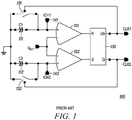
- FIG. 1 is a schematic of a known current-controlled oscillator 100 that uses the traditional architecture to output clock signals CLK1 and CLK2.
- the known current-controlled oscillator (hereinafter, "known oscillator") 100 comprises comparator 101 , comparator 102 , capacitor 111 , capacitor 112 and a latch 130 .
- the known oscillator 100 also comprises a switch 131 coupled between a ground terminal and a non-inverted input terminal of comparator 101 , and a switch 132 coupled between the ground terminal and a non-inverted input terminal of comparator 102 .
- Switch 131 and switch 132 are controlled by CKL1 and CKL2, respectively.
- the known oscillator 100 employs a first current source (or high value resistor) ICH1 141 coupled to the non-inverted input terminal of comparator 101 , second current source (or high value resistor) ICH2 142 coupled to the non-inverted input terminal of comparator 102 , and a voltage reference V REF coupled to an inverted input terminal of comparator 101 and comparator 102 .
- a voltage at either of the non-inverted input terminal of comparator 101 and the non-inverted input terminal of comparator 102 reaches V REF .
- the voltage toggles the latch 130 .
- comparator 101 resets the latch 130 and comparator 102 sets the latch.
- Each comparator 101 and 102 generates only short pulses to toggle the latch 130 .
- Each comparator 101 and 102 toggles the latch 130 once every cycle. In a half cycle, capacitor 111 is charged and capacitor 112 is grounded. In a next half cycle, capacitor 112 is charged and capacitor 111 is grounded. Comparator 101 and 102 are both in a frequency-generation path of the known oscillator 100 .
- the known oscillator 100 uses only one voltage reference V REF , some other known current-controlled oscillators disadvantageously require more than one voltage reference.
- the current-controlled oscillators in accordance with the invention address this requirement, by employing a single comparator in a frequency generation path.
- a single comparator and a single current source (or high value resistor) in the frequency generation path the power consumption of current-controlled oscillators in accordance with the invention can be a little as half of the power consumption of known current-controlled oscillators.
- the current-controlled oscillators in accordance with the invention reduce area, decrease power consumption and have performance advantages.
- the single comparator architecture in the frequency generation path contributes to make the 50% duty cycle of the current-controlled oscillators in accordance with the invention closer to ideal because a mismatch between two comparators is not possible and a mismatch between two current sources is not possible.
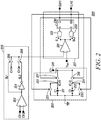
- FIG. 2 is a schematic of a current-controlled oscillator 200 in accordance with one embodiment of the invention.
- the current-controlled oscillator (hereinafter, "oscillator") 200 is a relaxation oscillator because its non-linear switched nature produces a non-sinusoidal repetitive output signal, such as a triangle wave or square wave.
- the oscillator 200 outputs clocks signals CLK1 and CKL2.
- the oscillator 200 is disposed in a single die as an integrated circuit.
- the oscillator 200 comprises a ramp voltage generating sub-circuit 203 , a ramp voltage selecting sub-circuit 205 and a switching signal generating sub-circuit 207 .
- the switching signal generating sub-circuit 207 comprises a comparator 201 that is in a frequency generation path of the oscillator 200 .
- the ramp voltage selecting sub-circuit 205 comprises a comparator 202 that is not in the frequency generation path.
- the ramp voltage generating sub-circuit 203 comprises capacitor 211 coupled between a ground terminal and an ICH1 node 213 , and capacitor 212 coupled between the ground terminal and an ICH2 node 214 .
- Capacitors 211 and 212 are identical in size and value. In one embodiment, capacitors 211 and 212 have a value of 1 ⁇ F.
- the capacitors 211 and 212 are disposed in the die of the integrated circuit of the oscillator 200. In the oscillator 200 attainment of a 50% duty cycle relies on matching of capacitors 211 and 212 (and not on matching of current sources or comparators as with the known oscillator 100 ), and, if there is a mismatch of the capacitors, the duty cycle typically varies from ideal by no more than 0.5%.
- the ramp voltage generating sub-circuit 203 also comprises a switch 217 coupled between node ICH1 213 and an input terminal ICH 241 , and a switch 218 coupled between node ICH2 214 and the input terminal ICH 241 .
- Input terminal ICH 241 is coupled to a current source (not shown).
- Switch 217 and switch 218 are controlled by the clock signals CLK1 and CLK2, respectively.
- a value of the current source ranges from approximately 10 ⁇ A to approximately 11 ⁇ A.
- the oscillator 200 advantageously requires only one current source.
- the ramp voltage generating sub-circuit 203 further comprises switch 231 coupled between the ICH1 node 213 and the ground terminal, and a switch 232 coupled between the ICH2 node 214 the ground terminal.
- Switch 231 is controlled by CLK2
- switch 232 is controlled by CLK1.
- the ramp voltage generating sub-circuit 203 Based on the states of switches 217 , 218 , 231 and 232 , the ramp voltage generating sub-circuit 203 generates, during alternate cycles, a first ramp voltage at node ICH1 213 based on a voltage across capacitor C1 211 , and a second ramp voltage at node ICH2 214 based on a voltage across capacitor C2 212 .
- the first and second ramp voltages are coupled to the ramp voltage selecting sub-circuit 205 .
- the value of the current source, the value of the capacitors C1 201 and C2 202 , and the value of V REF control the frequency of oscillation of the oscillator 200 , such that the higher is the value of the current source coupled to input terminal ICH 241 , the higher is the frequency of oscillation.
- the oscillator 200 operates at 16MHz. In another embodiment, the oscillator 200 operates at 64MHz. Other frequencies of oscillation are foreseeable.
- An inverted input terminal of the comparator 201 is coupled to a voltage reference V REF .
- V REF is approximately 0.3V and originates in a circuit that is not subject of this invention.
- the oscillator 200 advantageously requires only one voltage reference.
- the ramp voltage selecting sub-circuit 205 comprises a comparator 202 having a non-inverted input terminal for receiving the first ramp voltage, an inverted input terminal for receiving the second ramp voltage and an output terminal for producing an SL1 signal.
- the ramp voltage selecting sub-circuit 205 comprises an analog switch 206 coupled between the ICH1 node 213 and a non-inverted input terminal of comparator 201 of the switching signal generating sub-circuit 207 .
- the output terminal of comparator 202 is also coupled to an inverter 204 whose output is a SL2 signal. Comparator 202 evaluates the ramp voltages generated by the ramp voltage generating sub-circuit 203 .
- the ramp voltage selecting sub-circuit 205 further comprises an analog switch 208 coupled between the ICH2 node 214 and the non-inverted input terminal of comparator 201 of the switching signal generating sub-circuit 207 .
- Switch 206 is controlled by signal SL1 and switch 208 is controlled by signal SL2 such that, at any time, one of node ICH1 213 and node ICH2 214 is coupled to the switching signal generating sub-circuit 207 .
- Switches 206 and 208 in conjunction with signals SL1 and SL2 form an analog multiplexer. Therefore, ramp voltage selecting sub-circuit 205 causes the switching signal generating sub-circuit 207 to receive one of the first ramp voltage and the second ramp voltage that is generated by the ramp voltage generating sub-circuit 203 .
- comparator 202 is not in the frequency generation path it advantageously does not need to be a fast as comparator 201 .
- SL1 can stay low (logic "0") as long as CLK1 remains high.
- T DELAY (see FIG. 3 ) can be as long as almost half a cycle. Therefore, comparator 202 can be much slower than comparator 201 .
- Comparator 201 needs receive the voltage of one of capacitor C1 201 and capacitor C2 202 only at the moment that the voltage of each capacitor reaches V REF . During T DELAY , the comparator 201 is receiving the voltage of the capacitor that had been grounded in the previous half cycle.
- comparator 202 When the switches that are coupled to nodes ICH1 213 and ICH2 214 swap states, and comparator 202 toggles. Because comparator 202 consumes a small amount of current relative to the current consumed by comparator 201 , the time it takes (T DELAY ) before comparator 202 toggles may be few nanoseconds to tens of nanoseconds. T DELAY can be any value provided that comparator 202 toggles prior to a next swap of the states of the switches that are coupled to nodes ICH1 213 and ICH2 214 .
- the output of comparator 202 is connected to a non-overlapping clock circuit (not shown) to control switches 206 and 208 that send one of the voltage at node ICH1 213 and ICH2 214 to the non-inverted input of comparator 201 .
- the non-overlapping clock circuit if present, prevents both control switches 206 and 208 from being closed at a same time. In other words, the optional non-overlapping clock circuit assures that before control switch 208 is closed, control switch 206 is open.
- the switching signal generating sub-circuit 207 comprises comparator 201 having a non-inverted input terminal coupled to the ramp voltage selecting sub-circuit 205 and an inverted input terminal coupled to a voltage reference V REF .
- An output terminal of comparator 201 is coupled to an R (reset) input pin of a latch 230 through an analog switch and to an S (set) input pin of the latch through an analog switch 222 .
- Switch 221 is controlled by the output signal SL1 of the comparator 202
- switch 222 is controlled by the output signal SL2 of the inverter 204 such that, at any time, the output terminal of comparator 201 is coupled to one of the R input pin of latch 230 and the S input pin of the latch.
- comparator 202 causes an output of comparator 201 to be directed to one of the R input pin and the S input pin of the latch 230 .
- a Qb output pin of the latch 230 provides the CLK1 signal, and a Q output pin of the latch provides the CLK2 signal.
- each of switches 221 and 222 is implemented as an AND gate. Switches 221 and 222 in conjunction with signals SL1 and SL2 form an analog demultiplexer.
- Comparator 201 toggles the latch 230 every half cycle. Comparator 202 merely selects which input (R or S) of the latch 230 the comparator 201 will drive, which allows comparator 202 to operate more slowly (and consume less current) than comparator 201 and more slowly (and consume less current) than comparators 101 and 102 of the known oscillator 100 . Comparator 202 also selects which node (ICH1 213 or ICH2 214 ) comparator 201 compares against V REF .
- comparators 201 and 202 are exactly the same type, and comparator 202 is made to be slower by biasing it with lower currents.
- a bias input current to each comparator 201 and 202 is not shown in the drawings but is well known to persons skilled in the art.
- Oscillators such as the oscillator 200 are often used as an internal RC oscillator within a power management system.
- An internal RC oscillator is regularly turned on whenever a power management controller (PMC) of an integrated circuit performs operations that involves a state machine.
- the internal RC oscillator provides a clock for the state machine of the PMC even when an analog portion of the PMC is in an ultra-low-power mode which is defined as I DD being less than 500nA.
- I DD being less than 500nA.
- the internal RC oscillator is turned on even when the PMC is in the ultra-low-power mode. Therefore, saving a couple of ⁇ A is important to preserve low power characteristics of the PMC system. Therefore, saving several ⁇ A in an oscillator such as the oscillator 200 is important to maintain a low power profile of the PMC system.
- the architecture of the oscillator 200 allows a size of comparator 202 , as well as its power consumption, to be advantageously reduced relative to a size of comparator 201 , in case area savings is important.
- the size of comparator 202 may be similar to the size of comparator 201 , or even of exactly the same type, but biased with a lower current, in case area savings is not important.
- Comparator 201 is a high-speed comparator; however, comparator 202 does not need to be a high speed comparator.
- speed of a comparator, it is meant the propagation delay of the comparator.
- the propagation delay of a comparator is generally the same for a given bias current. As a rule of thumb, the propagation delay should be 1/10 of the clock period.
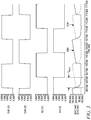
- FIG. 3 is a graph of signals present in a simulation of the oscillator 200 operating at 64MHz.
- the output signal SL1 from comparator 202 changes state when the voltage at node ICH1 213 and the voltage at node ICH2 214 crosses each other (the voltage at ICH1 213 rising and the voltage at ICH2 214 being reset to ground).
- comparator 202 is a low speed comparator, its switching delay T DELAY is naturally longer than the switching delay of a high speed comparator, such as comparator 201 .
- the bias current of the comparator 201 when the oscillator 200 is operating at 16MHz is approximately 10 ⁇ A.
- the bias current of the comparator 202 when the oscillator 200 is operating at 16MHz is advantageously only approximately 2 ⁇ A. Therefore, when the oscillator 200 is operating at 16MHz, comparators 201 and 202 would consume a total of approximately 12 ⁇ A. In contrast, if the known oscillator 100 were to operate at 16MHz, comparators 101 and 102 would consume approximately 10 ⁇ A each, for a total of approximately 20 ⁇ A. Consequently, at 16MHz, the current saving of oscillator 200 versus known oscillator 100 is approximately 40% depending on the process corner. In a simulation of the oscillator 200 , the total current consumption of the oscillator at 16MHz approximately.
- the bias current of the comparator 201 when the oscillator 200 is operating at 64MHz is approximately 18 ⁇ A.
- the bias current of the comparator 202 when the oscillator 200 is operating at 64MHz is advantageously only approximately 10 ⁇ A. Therefore, when the oscillator 200 is operating at 64MHz, comparators 201 and 202 would consume a total of approximately 28 ⁇ A. In contrast, if the known oscillator 100 were to operate at 64MHz, comparators 101 and 102 would consume approximately 18 ⁇ A each, for a total of approximately 36 ⁇ A. Consequently, at 64MHz, the current saving of oscillator 200 versus known oscillator 100 is approximately 22% depending on the process corner.
- FIG. 4 is a schematic of a current-controlled oscillator 400 in accordance with another embodiment of the invention.
- the current-controlled oscillator (hereinafter, "oscillator") 400 is a relaxation oscillator.
- the oscillator 400 outputs clocks signals CLK1 and CKL2.
- the oscillator 400 is disposed in a single die as an integrated circuit.
- the oscillator 400 comprises a single comparator 401 , logic control circuitry 402 , and a ramp voltage generating sub-circuit 403 .
- the ramp voltage generating sub-circuit 403 generates a ramp voltage V RAMP .
- the single comparator 401 which is in a frequency generation path of the oscillator 400 , performs threshold detection of V RAMP relative to a reference voltage V REF .
- the logic control circuitry 402 performs selection of V RAMP emanating from one of capacitor C1 411 and capacitor C2 412 .
- the ramp voltage generating sub-circuit 403 includes analog switches 417 , 418 , 431 and 432 .
- Capacitor C1 411 , capacitor C2 412 and switches 417 , 418 , 431 and 432 are coupled in a manner analogous to how similarly-located components are coupled in FIG. 2 .
- a current source (not shown) is coupled to an input terminal ICH 420 and supplies current to capacitor C1 411 and capacitor C2 412 , but not at the same time.
- a value of the current source controls, in part, a frequency of oscillator of the oscillator 400 .
- Switches 417 , 418 , 431 and 432 may change accordingly to the embodiment (NMOS, PMOS or both) due to physical properties required to fulfill design conditions.
- switches 417 and 418 with capital letter H represent switches that are closed when a control signal for the switch is logic "0" and open when the control signal for the switch is logic "1”
- switches 431 and 432 with capital letter L represent switches that are closed when a control signal for the switch is logic "1” and open when the control signal for the switch is logic "0”.
- the switch 431 is used to connect node ICH1 413 to a ground terminal depending on a value of a Q1b signal.
- the switch 432 is used to connect node ICH2 414 to the ground terminal depending on a value of a Q1 signal.
- the switches 417 and 418 are used to connect one of node ICH1 413 and node ICH2 414 to the comparator 401 , depending on values of the Q1 signal and the Q1b signal.
- the comparator 401 includes a non-inverted input terminal for receiving the V RAMP signal from the ramp voltage generating sub-circuit 403 , an inverted input terminal for receiving a reference voltage V REF and an output terminal for outputting a CMP signal.
- the logic control circuitry 402 comprises a demultiplexer 442 , latch 444 and latch 446 .
- the oscillator 400 advantageously uses latches 444 and 446 instead of flip-flops.
- the demultiplexer 442 has an input data line for receiving the CMP signal from the comparator 401 , a Z1 output line for outputting a S1 signal, a Z0 output line for outputting a R1 signal and a select input pin for receiving a SELQ signal. If the select input pin receives a logic "0" signal, the signal received at the input data line is routed to the Z0 output line, otherwise it is routed to the Z1 output line.
- the latch 444 includes an S input for receiving the S1 signal, a R input for receiving the R1 signal, a Q output for outputting a Q1 signal and a Qb output for outputting a Q1b signal.
- the latch 444 also includes an Rb input for receiving the START signal.
- the latch 446 includes an S input for receiving the Q1 signal, an R input for receiving the Q1b signal, an inverted enable input ENb, which gates the S and R inputs when 0, for receiving the CMP signal, and a Q output for outputting a SELQ signal.
- the latch 446 also includes a Sb input for receiving the START signal.
- the Qb output of latch 446 is not used.
- FIG. 4 is based on grounded capacitors, other embodiments of the oscillator 400 using capacitors (and reference) connected to V DD are also possible without changes in the logic control circuitry 402 .
- the oscillator 400 includes start-up circuitry (not shown), which receives the START signal to assure that capacitor C1 411 and C2 412 are discharged while the START signal is "0".
- the start-up circuitry causes the input terminal ICH 420 to be un-coupled from the current source and causes a V RAMP node 421 to be coupled to ground.
- the start-up circuitry plays no roles during oscillation.
- Signal S1 is asserted, toggles (sets) latch 444 making Q1 to be asserted and de-asserting Q1b.
- This state change "re-wires" the switch connections opening switch 431 , closing switch 417 , followed by closing switch 432 and opening switch 418 .
- the state of Q1 and SELQ are [1, 1].
- V RAMP is connected to ICH1 and goes to the potential of capacitor C1 411 (discharged), signal CMP then is de-asserted.
- Latch 446 is enabled and toggles with new values of Q1 and Q1b.
- Q1 and SELQ are [1, 0].
- Signal SELQ de-asserted redirects signal CMP to signal R1.
- the current source is connected to capacitor C1 411 (charging) while C2 412 is discharged (connected to ground in this embodiment).
- V RAMP rises again as C1 411 is charging.
- latch 444 toggles (resets) as signal R1 is asserted by signal CMP via demultiplexer 442 , then Q1 and SELQ will be [0, 0].
- the signal CMP is de-asserted and the signal SELQ is updated again starting a new cycle with C2 412 being charged, back again to state Q1, SELQ as [0, 1]. This cycle repetition creates the oscillation behavior.
- Latch 446 "gates" demultiplexer 442 , such that it is only allowed to toggle after latch 444 changed state and the comparator 401 returned to 0. This precaution avoids metastability conditions that could cause Q1 and Q1b to toggle independently of exchange of capacitors 411 and 412 .
- the architecture of the oscillator 400 prohibits SELQ from toggling when CMP is still at logic "1".
- FIG. 5 is a state diagram that represents operation of the oscillator 400 in a more abstract way.
- the state diagram has inputs signals START and CMP and has states defined by values of Q1 and SELQ.
- the oscillation is performed cyclically in four states, S1 to S4, and then starts over again and again.
- Two states are associated with each capacitor: S1 and S2 with C2 412 , and S3 and S4 with C1 411 .
- State S1 corresponds to an idle condition if START is de-asserted, otherwise corresponds to the instant where C2 412 is connected to V RAMP and charges (while C1 411 is disconnected and remains discharged).
- State S3 is the state where C1 411 is connected to V RAMP and charges (while C2 412 is disconnected and remains discharged).
- the oscillator 400 stays most of time in one of these two states (charging a capacitor).
- the states of S2 and S4 correspond to a short period transition used to assure that demultiplexer signal control SELQ holds its value until a swap between C1 411 and C2 412 (or vice-versa) is done.
- the signal SELQ used to control demultiplexer 442 , is precisely defined and does not depend on delay-based solutions used in some known current-controlled oscillators.
- FIG. 6 is a graph of signals present in a simulation of the oscillator 400 .
- the basic signals are presented: Q1, Q1b, START, CMP, V RAMP , ICH1 and ICH2.
- Signals "Q1" or “Q1b” when connected to output buffers correspond to the outputs of the oscillator 400 .
- V DD is 1.8V and the frequency of oscillation is approximately 5MHz.
- the single current source, ICH, used by the oscillator 400 may change from 1 ⁇ A to 250 ⁇ A.
- FIG. 7 shows detail of a transition, including corresponding states, of the signals present in a simulation of the oscillator 400 .
- FIG. 7 shows CMP being asserted and causing state transition from S1 to S2.
- C2 412 and C1 411 are swapped (ICH2 and ICH1), CMP is de-asserted and SELQ is updated and there is a state transition from S2 to S3. The same kind of behavior would be seen if another snapshot of next CMP transition were taken (from state S3 to state S4 to state S1).
- Latch 444 is asserted/de-asserted by a voltage level of signal CMP, so the signal CMP lasts long enough to allow the change in the latch to occur. This is straight forward because the input of the comparator 401 changes only after latch 444 is updated and a response of the comparator is much slower than gate delays within the latch. Gate delays within the latches 444 and 446 are less than 1ns.
- a bias input current to comparator 401 is not shown in the drawings but is well known to persons skilled in the art.
- a power supply to the logic control circuitry 402 and to the switches is not shown in the drawings but is well known to persons skilled in the art.
- the design of the oscillator 400 assures that latches 444 and 446 are not asserted at a same time.
- oscillator 400 is used as a precision current-to-frequency converter.
- the oscillators 200 and 400 reduce a number of critical components while improving robustness.
- switches of oscillators 200 and 400 are shown pictorially as single-throw switches, each of them are, in fact, NMOS or PMOS transistors configured in a manner well known to persons skilled in the art. Other types of electronic devices acting as switches of the oscillators 200 and 400 are foreseeable.
- the oscillators 200 and 400 are portable to any technology in use (bipolar, bulk complementary metal oxide semiconductor, silicon on insulator, etc.).
- the oscillators 200 and 400 can be employed where a robust and precise controlled-current oscillator is required with area and power gains when compared traditional architectures.
- the oscillators 200 and 400 can be employed as voltage controller oscillators if a voltage-to-current converter is used to feed the input current.
- a current-controlled oscillator receives an input current.
- Ramp voltage generating circuitry generates first and second ramp voltages in response to the input current. Selecting circuitry selects one of the first and second ramp voltages depending on their relative values.
- Switching circuitry receives a selected ramp voltage, generates a signal based on the selected ramp voltage relative to a reference voltage, and outputs a clock signal.
- a comparator receives the reference voltage, one of the first and second ramp voltages, and outputs a comparison signal.
- Logic circuitry controls the ramp voltage generating circuitry to output one of the ramp voltages during one half of a clock cycle and to output the other ramp voltage during another half cycle of the clock signal based on the comparison signal and logic states of the logic circuitry.
- Coupled is defined as “connected”, and encompasses the coupling of devices that may be physically, electrically or communicatively connected, although the coupling may not necessarily be directly, and not necessarily be mechanically.
- Configured to describes hardware, software or a combination of hardware and software that is adapted to, set up, arranged, built, composed, constructed, designed or that has any combination of these characteristics to carry out a given function.
Landscapes
- Engineering & Computer Science (AREA)
- Theoretical Computer Science (AREA)
- Power Engineering (AREA)
- Physics & Mathematics (AREA)
- General Engineering & Computer Science (AREA)
- General Physics & Mathematics (AREA)
- Manipulation Of Pulses (AREA)
- Analogue/Digital Conversion (AREA)
- Stabilization Of Oscillater, Synchronisation, Frequency Synthesizers (AREA)
Abstract
Description
- This invention relates generally to electrical circuits, and more specifically to a current-controlled oscillator.
- A traditional architecture for a current-controlled oscillator, which uses two current sources, two comparators and a latch, is popular due to a trade-off between simplicity and performance. However, the traditional architecture requires two current sources or resistors. Furthermore, the two comparators of the traditional architecture occupy a large area for low cost designs or consume a considerable amount of current for low power applications.
-
FIG. 1 is a schematic of a known current-controlledoscillator 100 that uses the traditional architecture to output clock signals CLK1 and CLK2. The known current-controlled oscillator (hereinafter, "known oscillator") 100 comprisescomparator 101,comparator 102, capacitor 111,capacitor 112 and alatch 130. The knownoscillator 100 also comprises aswitch 131 coupled between a ground terminal and a non-inverted input terminal ofcomparator 101, and aswitch 132 coupled between the ground terminal and a non-inverted input terminal ofcomparator 102. Switch 131 andswitch 132 are controlled by CKL1 and CKL2, respectively. The knownoscillator 100 employs a first current source (or high value resistor) ICH1 141 coupled to the non-inverted input terminal ofcomparator 101, second current source (or high value resistor)ICH2 142 coupled to the non-inverted input terminal ofcomparator 102, and a voltage reference VREF coupled to an inverted input terminal ofcomparator 101 andcomparator 102. Whenever a voltage at either of the non-inverted input terminal ofcomparator 101 and the non-inverted input terminal ofcomparator 102 reaches VREF, the voltage toggles thelatch 130. For example,comparator 101 resets thelatch 130 andcomparator 102 sets the latch. Eachcomparator latch 130. Eachcomparator latch 130 once every cycle. In a half cycle, capacitor 111 is charged andcapacitor 112 is grounded. In a next half cycle,capacitor 112 is charged and capacitor 111 is grounded.Comparator oscillator 100. - In the known
oscillator 100 attainment of a 50% duty cycle relies on matching of the first and secondcurrent sources comparators - Although the known
oscillator 100 uses only one voltage reference VREF, some other known current-controlled oscillators disadvantageously require more than one voltage reference. - The present invention is illustrated by way of example and is not limited by the accompanying figures, in which like references indicate similar elements.
-
FIG. 1 is a schematic of a known current-controlled oscillator. -
FIG. 2 is a schematic of a current-controlled oscillator in accordance with one embodiment of the invention. -
FIG. 3 is a graph of signals present in a simulation of the current-controlled oscillator shown inFIG. 2 . -
FIG. 4 is a schematic of a current-controlled oscillator in accordance with another embodiment of the invention. -
FIG. 5 is a state diagram that represents operation of the current-controlled oscillator shown inFIG. 4 . -
FIG. 6 is a graph of signals present in a simulation of the current-controlled oscillator shown inFIG. 4 . -
FIG. 7 shows a transition detail of the signals present in a simulation of the current-controlled oscillator shown inFIG. 4 . - New integrated circuit designs require higher efficiency where lower current consumption and smaller area are as important as functionality and performance. The current-controlled oscillators in accordance with the invention address this requirement, by employing a single comparator in a frequency generation path. By employing a single comparator and a single current source (or high value resistor) in the frequency generation path, the power consumption of current-controlled oscillators in accordance with the invention can be a little as half of the power consumption of known current-controlled oscillators. The current-controlled oscillators in accordance with the invention reduce area, decrease power consumption and have performance advantages. The single comparator architecture in the frequency generation path contributes to make the 50% duty cycle of the current-controlled oscillators in accordance with the invention closer to ideal because a mismatch between two comparators is not possible and a mismatch between two current sources is not possible.
-
FIG. 2 is a schematic of a current-controlledoscillator 200 in accordance with one embodiment of the invention. The current-controlled oscillator (hereinafter, "oscillator") 200 is a relaxation oscillator because its non-linear switched nature produces a non-sinusoidal repetitive output signal, such as a triangle wave or square wave. Theoscillator 200 outputs clocks signals CLK1 and CKL2. In one embodiment, theoscillator 200 is disposed in a single die as an integrated circuit. - The
oscillator 200 comprises a rampvoltage generating sub-circuit 203, a rampvoltage selecting sub-circuit 205 and a switchingsignal generating sub-circuit 207. The switchingsignal generating sub-circuit 207 comprises acomparator 201 that is in a frequency generation path of theoscillator 200. The rampvoltage selecting sub-circuit 205 comprises acomparator 202 that is not in the frequency generation path. - The ramp
voltage generating sub-circuit 203 comprisescapacitor 211 coupled between a ground terminal and anICH1 node 213, andcapacitor 212 coupled between the ground terminal and anICH2 node 214.Capacitors capacitors capacitors oscillator 200. In theoscillator 200 attainment of a 50% duty cycle relies on matching ofcapacitors 211 and 212 (and not on matching of current sources or comparators as with the known oscillator 100), and, if there is a mismatch of the capacitors, the duty cycle typically varies from ideal by no more than 0.5%. - The ramp
voltage generating sub-circuit 203 also comprises aswitch 217 coupled between node ICH1 213 and an input terminal ICH 241, and aswitch 218 coupled betweennode ICH2 214 and theinput terminal ICH 241.Input terminal ICH 241 is coupled to a current source (not shown). Switch 217 andswitch 218 are controlled by the clock signals CLK1 and CLK2, respectively. As a result, one of node ICH1 213 and node ICH2 214 is connected to the current source at any time. In one embodiment, a value of the current source ranges from approximately 10µA to approximately 11 µA. Theoscillator 200 advantageously requires only one current source. - The ramp
voltage generating sub-circuit 203 further comprisesswitch 231 coupled between theICH1 node 213 and the ground terminal, and aswitch 232 coupled between theICH2 node 214 the ground terminal.Switch 231 is controlled by CLK2, andswitch 232 is controlled by CLK1. Based on the states ofswitches voltage generating sub-circuit 203 generates, during alternate cycles, a first ramp voltage atnode ICH1 213 based on a voltage acrosscapacitor C1 211, and a second ramp voltage atnode ICH2 214 based on a voltage acrosscapacitor C2 212. The first and second ramp voltages are coupled to the rampvoltage selecting sub-circuit 205. - The value of the current source, the value of the
capacitors C1 201 andC2 202, and the value of VREF control the frequency of oscillation of theoscillator 200, such that the higher is the value of the current source coupled toinput terminal ICH 241, the higher is the frequency of oscillation. The higher is the value of capacitance or the value of VREF, the lower is the frequency of oscillation. Neglecting switching delays, an ideal frequency of oscillation is related to the control current by the following equation:
- In one embodiment, the
oscillator 200 operates at 16MHz. In another embodiment, theoscillator 200 operates at 64MHz. Other frequencies of oscillation are foreseeable. - An inverted input terminal of the
comparator 201 is coupled to a voltage reference VREF. In one embodiment, VREF is approximately 0.3V and originates in a circuit that is not subject of this invention. Unlike some known current-controlled oscillators, theoscillator 200 advantageously requires only one voltage reference. - The ramp
voltage selecting sub-circuit 205 comprises acomparator 202 having a non-inverted input terminal for receiving the first ramp voltage, an inverted input terminal for receiving the second ramp voltage and an output terminal for producing an SL1 signal. The rampvoltage selecting sub-circuit 205 comprises ananalog switch 206 coupled between theICH1 node 213 and a non-inverted input terminal ofcomparator 201 of the switchingsignal generating sub-circuit 207. The output terminal ofcomparator 202 is also coupled to aninverter 204 whose output is a SL2 signal.Comparator 202 evaluates the ramp voltages generated by the rampvoltage generating sub-circuit 203. The ramp voltage selecting sub-circuit 205 further comprises ananalog switch 208 coupled between theICH2 node 214 and the non-inverted input terminal ofcomparator 201 of the switchingsignal generating sub-circuit 207.Switch 206 is controlled by signal SL1 and switch 208 is controlled by signal SL2 such that, at any time, one ofnode ICH1 213 andnode ICH2 214 is coupled to the switchingsignal generating sub-circuit 207.Switches voltage generating sub-circuit 203. - Because
comparator 202 is not in the frequency generation path it advantageously does not need to be a fast ascomparator 201. For example, after CLK1 rises to logic "1", SL1 can stay low (logic "0") as long as CLK1 remains high. In other words, TDELAY (seeFIG. 3 ) can be as long as almost half a cycle. Therefore,comparator 202 can be much slower thancomparator 201.Comparator 201 needs receive the voltage of one ofcapacitor C1 201 andcapacitor C2 202 only at the moment that the voltage of each capacitor reaches VREF. During TDELAY, thecomparator 201 is receiving the voltage of the capacitor that had been grounded in the previous half cycle. When the switches that are coupled tonodes ICH1 213 andICH2 214 swap states, andcomparator 202 toggles. Becausecomparator 202 consumes a small amount of current relative to the current consumed bycomparator 201, the time it takes (TDELAY) beforecomparator 202 toggles may be few nanoseconds to tens of nanoseconds. TDELAY can be any value provided thatcomparator 202 toggles prior to a next swap of the states of the switches that are coupled tonodes ICH1 213 andICH2 214. - In another embodiment (not shown) of the ramp
voltage selecting sub-circuit 205, the output ofcomparator 202 is connected to a non-overlapping clock circuit (not shown) to controlswitches node ICH1 213 andICH2 214 to the non-inverted input ofcomparator 201. The non-overlapping clock circuit, if present, prevents bothcontrol switches control switch 208 is closed,control switch 206 is open. - The switching
signal generating sub-circuit 207 comprisescomparator 201 having a non-inverted input terminal coupled to the rampvoltage selecting sub-circuit 205 and an inverted input terminal coupled to a voltage reference VREF. An output terminal ofcomparator 201 is coupled to an R (reset) input pin of alatch 230 through an analog switch and to an S (set) input pin of the latch through ananalog switch 222.Switch 221 is controlled by the output signal SL1 of thecomparator 202, and switch 222 is controlled by the output signal SL2 of theinverter 204 such that, at any time, the output terminal ofcomparator 201 is coupled to one of the R input pin oflatch 230 and the S input pin of the latch. Consequently,comparator 202 causes an output ofcomparator 201 to be directed to one of the R input pin and the S input pin of thelatch 230. A Qb output pin of thelatch 230 provides the CLK1 signal, and a Q output pin of the latch provides the CLK2 signal. In the illustrated embodiment, each ofswitches Switches -
Comparator 201 toggles thelatch 230 every half cycle.Comparator 202 merely selects which input (R or S) of thelatch 230 thecomparator 201 will drive, which allowscomparator 202 to operate more slowly (and consume less current) thancomparator 201 and more slowly (and consume less current) thancomparators oscillator 100.Comparator 202 also selects which node (ICH1 213 or ICH2 214)comparator 201 compares against VREF. - With known current-controlled oscillators, such as the known
oscillator 100, a total current consumption of the comparators is approximately 40µA. With theoscillator 200, the total current consumption of the comparators is 22µA becausecomparator 202 does not need to be as fast or accurate ascomparator 201 needs to be. In one embodiment,comparators comparator 202 is made to be slower by biasing it with lower currents. A bias input current to eachcomparator - Oscillators such as the
oscillator 200 are often used as an internal RC oscillator within a power management system. An internal RC oscillator is regularly turned on whenever a power management controller (PMC) of an integrated circuit performs operations that involves a state machine. The internal RC oscillator provides a clock for the state machine of the PMC even when an analog portion of the PMC is in an ultra-low-power mode which is defined as IDD being less than 500nA. In some applications, the internal RC oscillator is turned on even when the PMC is in the ultra-low-power mode. Therefore, saving a couple of µA is important to preserve low power characteristics of the PMC system. Therefore, saving several µA in an oscillator such as theoscillator 200 is important to maintain a low power profile of the PMC system. - The architecture of the
oscillator 200 allows a size ofcomparator 202, as well as its power consumption, to be advantageously reduced relative to a size ofcomparator 201, in case area savings is important. However, the size ofcomparator 202 may be similar to the size ofcomparator 201, or even of exactly the same type, but biased with a lower current, in case area savings is not important. -
Comparator 201 is a high-speed comparator; however,comparator 202 does not need to be a high speed comparator. By "speed" of a comparator, it is meant the propagation delay of the comparator. The propagation delay of a comparator is generally the same for a given bias current. As a rule of thumb, the propagation delay should be 1/10 of the clock period. -
FIG. 3 is a graph of signals present in a simulation of theoscillator 200 operating at 64MHz. The output signal SL1 fromcomparator 202 changes state when the voltage atnode ICH1 213 and the voltage atnode ICH2 214 crosses each other (the voltage atICH1 213 rising and the voltage atICH2 214 being reset to ground). Becausecomparator 202 is a low speed comparator, its switching delay TDELAY is naturally longer than the switching delay of a high speed comparator, such ascomparator 201. As a result,comparator 201 senses the voltage atnode ICH1 213 andICH2 214 only after a switching delay of 3ns to 5ns, in other words TDELAY = 3-5ns. - The bias current of the
comparator 201 when theoscillator 200 is operating at 16MHz is approximately 10µA. However, the bias current of thecomparator 202 when theoscillator 200 is operating at 16MHz is advantageously only approximately 2µA. Therefore, when theoscillator 200 is operating at 16MHz,comparators oscillator 100 were to operate at 16MHz,comparators oscillator 200 versus knownoscillator 100 is approximately 40% depending on the process corner. In a simulation of theoscillator 200, the total current consumption of the oscillator at 16MHz approximately. - The bias current of the
comparator 201 when theoscillator 200 is operating at 64MHz is approximately 18µA. However, the bias current of thecomparator 202 when theoscillator 200 is operating at 64MHz is advantageously only approximately 10µA. Therefore, when theoscillator 200 is operating at 64MHz,comparators oscillator 100 were to operate at 64MHz,comparators oscillator 200 versus knownoscillator 100 is approximately 22% depending on the process corner. -
FIG. 4 is a schematic of a current-controlledoscillator 400 in accordance with another embodiment of the invention. The current-controlled oscillator (hereinafter, "oscillator") 400 is a relaxation oscillator. Theoscillator 400 outputs clocks signals CLK1 and CKL2. In one embodiment, theoscillator 400 is disposed in a single die as an integrated circuit. Theoscillator 400 comprises asingle comparator 401,logic control circuitry 402, and a rampvoltage generating sub-circuit 403. The rampvoltage generating sub-circuit 403 generates a ramp voltage VRAMP. Thesingle comparator 401, which is in a frequency generation path of theoscillator 400, performs threshold detection of VRAMP relative to a reference voltage VREF. Thelogic control circuitry 402 performs selection of VRAMP emanating from one ofcapacitor C1 411 andcapacitor C2 412. - The ramp
voltage generating sub-circuit 403 includes analog switches 417, 418, 431 and 432.Capacitor C1 411,capacitor C2 412 and switches 417, 418, 431 and 432 are coupled in a manner analogous to how similarly-located components are coupled inFIG. 2 . A current source (not shown) is coupled to aninput terminal ICH 420 and supplies current tocapacitor C1 411 andcapacitor C2 412, but not at the same time. A value of the current source controls, in part, a frequency of oscillator of theoscillator 400. -
Switches switches switch 431 is used to connectnode ICH1 413 to a ground terminal depending on a value of a Q1b signal. Theswitch 432 is used to connectnode ICH2 414 to the ground terminal depending on a value of a Q1 signal. Theswitches node ICH1 413 andnode ICH2 414 to thecomparator 401, depending on values of the Q1 signal and the Q1b signal. - The
comparator 401 includes a non-inverted input terminal for receiving the VRAMP signal from the rampvoltage generating sub-circuit 403, an inverted input terminal for receiving a reference voltage VREF and an output terminal for outputting a CMP signal. - The
logic control circuitry 402 comprises ademultiplexer 442,latch 444 andlatch 446. Unlike some known current-controlled oscillators that use one or more flip-flops which do not account for possible timing issues, theoscillator 400 advantageously uses latches 444 and 446 instead of flip-flops. - The
demultiplexer 442 has an input data line for receiving the CMP signal from thecomparator 401, a Z1 output line for outputting a S1 signal, a Z0 output line for outputting a R1 signal and a select input pin for receiving a SELQ signal. If the select input pin receives a logic "0" signal, the signal received at the input data line is routed to the Z0 output line, otherwise it is routed to the Z1 output line. - The
latch 444 includes an S input for receiving the S1 signal, a R input for receiving the R1 signal, a Q output for outputting a Q1 signal and a Qb output for outputting a Q1b signal. Thelatch 444 also includes an Rb input for receiving the START signal. The Rb input has precedence over the other inputs to the latch and the Rb input forces a known and convenient initial state for logic in thelatch 444 when START=0, the known and convenient initial state being S=0, R=0, Q=0 and Qb=1. However, the Rb input plays no role during oscillation, i.e., when START=1 other than to allow the oscillation to occur and to continue. - The
latch 446 includes an S input for receiving the Q1 signal, an R input for receiving the Q1b signal, an inverted enable input ENb, which gates the S and R inputs when 0, for receiving the CMP signal, and a Q output for outputting a SELQ signal. Thelatch 446 also includes a Sb input for receiving the START signal. The Sb input has precedence over the other inputs to the latch and the Sb input forces a known and convenient initial state for logic in thelatch 446 when START=0, the known and convenient initial state being S=1, R=0, ENb=0 and Q=1. However, the Sb input plays no role during oscillation, i.e., when START=1 other than to allow the oscillation to occur and to continue. The Qb output oflatch 446 is not used. - The schematic of
FIG. 4 is based on grounded capacitors, other embodiments of theoscillator 400 using capacitors (and reference) connected to VDD are also possible without changes in thelogic control circuitry 402. - Operation of the
oscillator 400 is as follows. Beginning from instant where signal START is still de-asserted, signals Q1 and SELQ are forced to have the logical values [0, 1] respectively due to "0" logic level on pin Rb oflatch 444 and pin Sb oflatch 446. Theoscillator 400 includes start-up circuitry (not shown), which receives the START signal to assure thatcapacitor C1 411 andC2 412 are discharged while the START signal is "0". The start-up circuitry causes theinput terminal ICH 420 to be un-coupled from the current source and causes a VRAMP node 421 to be coupled to ground. The start-up circuitry plays no roles during oscillation. This combination of control signals and states causes switches 431 and 418 to be closed (and theircomplement switches capacitors C1 411 andC2 412 are discharged; wires VRAMP, ICH1 and ICH2 are grounded, and signal CMP is de-asserted. - The condition above remains unchanged while the START signal remains de-asserted. Once the START signal changes to asserted, the logic signals initially remain as is. As
capacitor C2 412 charges, wire VRAMP (wires ICH2 and VRAMP are shorted by switch 418) rises till reach the threshold ofcomparator 401 defined by VREF. In one embodiment, VREF = 1V. Once thecomparator 401 is asserted,latch 446 is momentarily disabled (input changes cannot be registered), and comparator signal CMP is routed insidedemultiplexer 442 to output pin Z1, reaching wire S1 to input S oflatch 444. Signal S1 is asserted, toggles (sets)latch 444 making Q1 to be asserted and de-asserting Q1b. This state change "re-wires" the switchconnections opening switch 431, closingswitch 417, followed by closingswitch 432 andopening switch 418. Now the state of Q1 and SELQ are [1, 1]. As the switches are changed, VRAMP is connected to ICH1 and goes to the potential of capacitor C1 411 (discharged), signal CMP then is de-asserted.Latch 446 is enabled and toggles with new values of Q1 and Q1b. Then, Q1 and SELQ are [1, 0]. Signal SELQ de-asserted redirects signal CMP to signal R1. Now, the current source is connected to capacitor C1 411 (charging) whileC2 412 is discharged (connected to ground in this embodiment). - With the new state defined by signals Q1 and SELQ to be respectively [1, 0], VRAMP rises again as
C1 411 is charging. The same sequence of events takes place with the only difference is that now latch 444 toggles (resets) as signal R1 is asserted by signal CMP viademultiplexer 442, then Q1 and SELQ will be [0, 0]. After the connection between the VRAMP node 421 andcapacitors C1 411 andC2 412 is swapped again, the signal CMP is de-asserted and the signal SELQ is updated again starting a new cycle withC2 412 being charged, back again to state Q1, SELQ as [0, 1]. This cycle repetition creates the oscillation behavior. -
Latch 446 "gates"demultiplexer 442, such that it is only allowed to toggle afterlatch 444 changed state and thecomparator 401 returned to 0. This precaution avoids metastability conditions that could cause Q1 and Q1b to toggle independently of exchange ofcapacitors oscillator 400 prohibits SELQ from toggling when CMP is still at logic "1". - In the
oscillator 400, changes in thedemultiplexer 442 are controlled by a combination of the output ofcomparator 401 and the state oflatch 444. Therefore, the time for changing thedemultiplexer 442 is limited only by the time it takes for thecomparator 401 to go to logic "0" plus the internal delay oflatch 446. The toggling of SELQ depends mostly on a time required forcomparator 401 to return to logic "0" because the internal delay oflatch 446 is much shorter than the time required for the comparator return to logic "0". -
FIG. 5 is a state diagram that represents operation of theoscillator 400 in a more abstract way. The state diagram has inputs signals START and CMP and has states defined by values of Q1 and SELQ. - The oscillation is performed cyclically in four states, S1 to S4, and then starts over again and again. Two states are associated with each capacitor: S1 and S2 with
C2 412, and S3 and S4 withC1 411. - State S1 corresponds to an idle condition if START is de-asserted, otherwise corresponds to the instant where
C2 412 is connected to VRAMP and charges (whileC1 411 is disconnected and remains discharged). State S3 is the state whereC1 411 is connected to VRAMP and charges (whileC2 412 is disconnected and remains discharged). Theoscillator 400 stays most of time in one of these two states (charging a capacitor). The states of S2 and S4 correspond to a short period transition used to assure that demultiplexer signal control SELQ holds its value until a swap betweenC1 411 and C2 412 (or vice-versa) is done. Once the swap betweenC1 411 and C2 412 (or vice-versa) is accomplished, CMP is naturally de-asserted and SELQ is updated safely. Thelatch 444 should be properly triggered: SET at end of state S1 and RESET at end of state S3. Otherwise, theoscillator 400 does not oscillate at a designed frequency or does not oscillate at all. - Advantageously, all logic states are defined. The signal SELQ, used to control
demultiplexer 442, is precisely defined and does not depend on delay-based solutions used in some known current-controlled oscillators. - The elements shown in
FIG. 4 and the states shown inFIG. 5 are related as follows. - (START=0) S1 -
C1 411 andC2 412 are discharged. - (START=1) S1 -
C2 412 charging andC1 411 shorted. Then, - (START=1) S2 - The output of
comparator 401 is asserted, and latch 444 changes state. This condition causes the capacitor banks to be swapped. Then, - (START=1) S3 -
Comparator 401 is de-asserted causes latch 446 to toggle, and then the input todemultiplexer 442 is changed safely because the output of thecomparator 401 is already de-asserted,C1 411 is charging andC2 412 is shorted. Then, - (START=1) S4 - The output of
comparator 401 is asserted, and latch 444 changes state, which causes the capacitor banks to be swapped. Then, - (START=1) S1 -
Comparator 401 is de-asserted causes latch 446 to toggle, and then the input todemultiplexer 442 is changed safely because the output of thecomparator 401 is already de-asserted,C2 412 is charging andC1 411 is shorted. Then, so on, S2, S3, S4, S1, S2, S3, S4, S1 ... -
Latch 444 is always available, so the CMP signal may be asserted at any time (or frequency). The only exception is when START=0. -
FIG. 6 is a graph of signals present in a simulation of theoscillator 400. The basic signals are presented: Q1, Q1b, START, CMP, VRAMP, ICH1 and ICH2. Signals "Q1" or "Q1b" when connected to output buffers correspond to the outputs of theoscillator 400. For this simulation, VDD is 1.8V and the frequency of oscillation is approximately 5MHz. - The single current source, ICH, used by the
oscillator 400 may change from 1µA to 250µA. When ICH=1µA, the frequency of operation is 40kHz. When ICH=250µA, the frequency of operation is 10MHz. -
FIG. 7 shows detail of a transition, including corresponding states, of the signals present in a simulation of theoscillator 400.FIG. 7 shows CMP being asserted and causing state transition from S1 to S2. AsC2 412 andC1 411 are swapped (ICH2 and ICH1), CMP is de-asserted and SELQ is updated and there is a state transition from S2 to S3. The same kind of behavior would be seen if another snapshot of next CMP transition were taken (from state S3 to state S4 to state S1). -
Latch 444 is asserted/de-asserted by a voltage level of signal CMP, so the signal CMP lasts long enough to allow the change in the latch to occur. This is straight forward because the input of thecomparator 401 changes only afterlatch 444 is updated and a response of the comparator is much slower than gate delays within the latch. Gate delays within thelatches - A bias input current to
comparator 401 is not shown in the drawings but is well known to persons skilled in the art. A power supply to thelogic control circuitry 402 and to the switches is not shown in the drawings but is well known to persons skilled in the art. - Advantageously, the design of the
oscillator 400 assures that latches 444 and 446 are not asserted at a same time. - In one application,
oscillator 400 is used as a precision current-to-frequency converter. - The
oscillators - Although the switches of
oscillators oscillators - The
oscillators oscillators oscillators - Embodiments may include combinations of features recited in the following numbered clauses:
- 1. A current-controlled oscillator, comprising: an input terminal for receiving an input current; a ramp voltage generating sub-circuit, coupled to the input terminal, for generating a first ramp voltage and a second ramp voltage, and for outputting one of the first ramp voltage and the second ramp voltage; a single comparator, having one input terminal coupled to the ramp voltage generating circuit for receiving the one of the first ramp voltage and the second ramp voltage, another input terminal coupled to a reference voltage and an output terminal for outputting a comparison signal based on a value of the one of the first ramp voltage and the second ramp voltage relative to a value of the reference voltage; and logic control circuitry for controlling the ramp voltage generating sub-circuit to output one of the first ramp voltage and the second ramp voltage during one half cycle of a clock signal and to output the other of the first ramp voltage and the second ramp voltage during another half cycle of the clock signal based on a value of the comparison signal and logic states of the logic control circuitry, wherein the logic control circuitry outputs clock signal CLK1 and clock signal CLK2.
- 2. The current-controlled oscillator of
clause 1, wherein the ramp voltage generating sub-circuit includes a first capacitor coupled between a ground terminal and a first ramp voltage node, and a second capacitor coupled between the ground terminal and a second ramp voltage node. - 3. The current-controlled oscillator of
clause 2, wherein the input current charges the first capacitor to produce the first ramp voltage at the first ramp voltage node and the input current charges the second capacitor to produce the second ramp voltage at the second ramp voltage node. - 4. The current-controlled oscillator of
clause 3, wherein the first ramp voltage node is switched between being coupled to the input terminal during one half cycle of the clock signal and being coupled to the ground terminal during another half cycle of the clock signal, and wherein the second ramp voltage node is switched between being coupled to the ground terminal during the one half cycle of the clock signal and being coupled to the input terminal during the another half cycle of the clock signal. - 5. The current-controlled oscillator of
clause 4, wherein the ramp voltage generating sub-circuit includes a first switch, controlled by clock signal CLK1, coupled between the first ramp voltage node and the input terminal, and a second switch, controlled by clock signal CLK2, coupled between the second ramp voltage node and the input terminal. - 6. The current-controlled oscillator of clause 5, wherein the ramp voltage generating sub-circuit includes a third switch controlled by clock signal CLK2 coupled between the input terminal and the ground terminal, and a fourth switch controlled by clock signal CLK1 coupled between the input terminal the ground terminal.
- 7. The current-controlled oscillator of clause 6, wherein the logic control circuitry includes a demultiplexer having an input data line for receiving the comparison signal from the single comparator, a Z1 output line for outputting a S1 signal, a Z0 output line for outputting a R1 signal, and a select input.
- 8. The current-controlled oscillator of clause 7, wherein the logic control circuitry includes a first latch having an S input for receiving the S1 signal, a R input for receiving the R1 signal, a Q output for outputting clock signal CLK1 and a Qb output for outputting clock signal CLK2.
- 9. The current-controlled oscillator of clause 8, wherein the logic control circuitry includes a second latch having an S input for receiving clock signal CLK1, a R input for receiving clock signal CLK2, an inverted enable input for receiving the comparison signal, and a Q output for outputting a SELQ signal to the select input of the first latch.
- A current-controlled oscillator receives an input current. Ramp voltage generating circuitry generates first and second ramp voltages in response to the input current. Selecting circuitry selects one of the first and second ramp voltages depending on their relative values. Switching circuitry receives a selected ramp voltage, generates a signal based on the selected ramp voltage relative to a reference voltage, and outputs a clock signal. In one embodiment, a comparator receives the reference voltage, one of the first and second ramp voltages, and outputs a comparison signal. Logic circuitry controls the ramp voltage generating circuitry to output one of the ramp voltages during one half of a clock cycle and to output the other ramp voltage during another half cycle of the clock signal based on the comparison signal and logic states of the logic circuitry.
- The term "coupled", as used herein, is defined as "connected", and encompasses the coupling of devices that may be physically, electrically or communicatively connected, although the coupling may not necessarily be directly, and not necessarily be mechanically. The term "configured to" describes hardware, software or a combination of hardware and software that is adapted to, set up, arranged, built, composed, constructed, designed or that has any combination of these characteristics to carry out a given function.
- The terms "a" or "an", as used herein, are defined as one or more than one. Also, the use of introductory phrases such as "at least one" and "one or more" in the claims should not be construed to imply that the introduction of another claim element by the indefinite articles "a" or "an" limits any particular claim containing such introduced claim element to inventions containing only one such element, even when the same claim includes the introductory phrases "one or more" or "at least one" and indefinite articles such as "a" or "an". The same holds true for the use of definite articles. Unless stated otherwise, terms such as "first" and "second" are used to arbitrarily distinguish between the elements such terms describe. Thus, these terms are not necessarily intended to indicate temporal or other prioritization of such elements.
- The Detailed Description section, and not the Abstract section, is intended to be used to interpret the claims. The Abstract section may set forth one or more but not all embodiments of the invention, and the Abstract section is not intended to limit the invention or the claims in any way.
- Although the invention is described herein with reference to specific embodiments, various modifications and changes can be made without departing from the scope of the present invention as set forth in the claims below. Accordingly, the specification and figures are to be regarded in an illustrative rather than a restrictive sense, and all such modifications are intended to be included within the scope of the present invention. Any benefits, advantages or solutions to problems that are described herein with regard to specific embodiments are not intended to be construed as a critical, required, or essential feature or element of any or all the claims.
Claims (11)
- A current-controlled oscillator, comprising:an input terminal for receiving an input current;a ramp voltage generating sub-circuit, coupled to the input terminal, for generating a first ramp voltage and a second ramp voltage during alternate cycles of a clock signal, wherein a frequency of the clock signal is based, in part, on a value of the input current;a ramp voltage selecting sub-circuit for selecting one of the first ramp voltage and the second ramp voltage depending on a value of the first ramp voltage relative to a value of the second ramp voltage; anda switching signal generating sub-circuit for receiving the selected ramp voltage and for generating a switching signal based on a value of the selected ramp voltage relative to a reference voltage,wherein the switching signal generating sub-circuit outputs clock signal CLK1 and clock signal CLK2.
- The current-controlled oscillator of claim 1, wherein the ramp voltage generating sub-circuit includes a first capacitor coupled between a ground terminal and a first ramp voltage node, and a second capacitor coupled between the ground terminal and a second ramp voltage node.
- The current-controlled oscillator of claim 1 or 2, wherein the input current charges the first capacitor to produce the first ramp voltage at the first ramp voltage node and the input current charges the second capacitor to produce the second ramp voltage at the second ramp voltage node.
- The current-controlled oscillator of any preceding claim, wherein the first ramp voltage node is switched between being coupled to the input terminal during one half cycle of the clock signal and being coupled to the ground terminal during another half cycle of the clock signal, and wherein the second ramp voltage node is switched between being coupled to the ground terminal during the one half cycle of the clock signal and being coupled to the input terminal during the another half cycle of the clock signal.
- The current-controlled oscillator of any preceding claim, wherein the ramp voltage generating sub-circuit includes a first switch, controlled by clock signal CLK1, coupled between the first ramp voltage node and the input terminal, and a second switch, controlled by clock signal CLK2, coupled between the second ramp voltage node and the input terminal.
- The current-controlled oscillator of any preceding claim, wherein the ramp voltage generating sub-circuit includes a third switch controlled by clock signal CLK2 coupled between the input terminal and the ground terminal, and a fourth switch controlled by clock signal CLK1 coupled between the input terminal the ground terminal.
- The current-controlled oscillator of any preceding claim, wherein the ramp voltage selecting sub-circuit includes a ramp voltage comparator for comparing the first ramp voltage and the second ramp voltage and for outputting a comparator output signal and wherein, based on comparison, the ramp voltage selecting sub-circuit outputs one of the first ramp voltage and the second ramp voltage.
- The current-controlled oscillator of any preceding claim, wherein the ramp voltage selecting sub-circuit includes a switch, controlled by the comparator output signal, coupled between the first ramp voltage node and an output of the ramp voltage selecting sub-circuit, and a switch, controlled by an inverted comparator output signal, coupled between the second ramp voltage node and the output of the ramp voltage selecting sub-circuit, such that, at any time, one of the first ramp voltage and the second ramp voltage is outputted by the ramp voltage selecting sub-circuit.
- The current-controlled oscillator of any preceding claim, wherein the switching signal generating sub-circuit includes a single comparator in a frequency generation path, the single comparator having a non-inverted input terminal coupled to the ramp voltage selecting sub-circuit for receiving one of the first ramp voltage and the second ramp voltage and having an inverted input terminal coupled to a voltage reference VREF.
- The current-controlled oscillator of claim 9, wherein an output terminal of the single comparator is coupled to an R input pin of a latch through a first switch controlled by the comparator output signal, and coupled to an S input pin of the latch through a second switch controlled by an inverted comparator output signal, such that, at any time, the output terminal of the single comparator is coupled to one of the R input pin of latch and the S input pin of the latch.
- The current-controlled oscillator of claim 10, wherein a Qb output pin of the latch provides clock signal CLK1 and a Q output pin of the latch provides clock signal CLK2.
Applications Claiming Priority (1)
| Application Number | Priority Date | Filing Date | Title |
|---|---|---|---|
| US16/406,256 US10734975B1 (en) | 2019-05-08 | 2019-05-08 | Current-controlled oscillator |
Publications (3)
| Publication Number | Publication Date |
|---|---|
| EP3736981A2 true EP3736981A2 (en) | 2020-11-11 |
| EP3736981A3 EP3736981A3 (en) | 2020-11-18 |
| EP3736981B1 EP3736981B1 (en) | 2024-02-21 |
Family
ID=70613672
Family Applications (1)
| Application Number | Title | Priority Date | Filing Date |
|---|---|---|---|
| EP20173294.8A Active EP3736981B1 (en) | 2019-05-08 | 2020-05-06 | Current-controlled oscillator |
Country Status (2)
| Country | Link |
|---|---|
| US (2) | US10734975B1 (en) |
| EP (1) | EP3736981B1 (en) |
Families Citing this family (3)
| Publication number | Priority date | Publication date | Assignee | Title |
|---|---|---|---|---|
| CN115333510A (en) * | 2022-08-19 | 2022-11-11 | 苏州聚元微电子股份有限公司 | A relaxation oscillator with a shared comparator |
| CN115622364B (en) * | 2022-09-27 | 2025-08-01 | 圣邦微电子(北京)股份有限公司 | Ramp generation circuit |
| CN117277999B (en) * | 2023-11-20 | 2024-02-09 | 中国电子科技集团公司第五十八研究所 | High-precision oscillator circuit with clock synchronization watchdog function |
Family Cites Families (27)
| Publication number | Priority date | Publication date | Assignee | Title |
|---|---|---|---|---|
| JPS61105111A (en) * | 1984-10-27 | 1986-05-23 | Toshiba Corp | Voltage controlled oscillating circuit |
| US5426384A (en) * | 1993-12-27 | 1995-06-20 | Motorola, Inc. | Voltage controlled oscillator (VCO) with symmetrical output and logic gate for use in same |
| JP2008306356A (en) * | 2007-06-06 | 2008-12-18 | Nec Electronics Corp | Triangle wave generator |
| ATE533230T1 (en) | 2008-09-05 | 2011-11-15 | Em Microelectronic Marin Sa | LOW VOLTAGE TILTING GENERATOR |
| US8115523B2 (en) * | 2008-12-12 | 2012-02-14 | Texas Instruments Incorporated | Circuit to spread the spectrum of a PWM signal |
| US8054141B2 (en) * | 2008-12-31 | 2011-11-08 | Stmicroelectronics, Inc. | Method and circuit for cancelling out comparator-delay in the relaxation oscillator |
| DE102009031144B4 (en) * | 2009-06-30 | 2013-08-01 | Austriamicrosystems Ag | Oscillator circuit and method for generating a clock signal |
| US8026770B2 (en) | 2009-07-01 | 2011-09-27 | Synaptics, Inc. | Relaxation oscillator |
| KR101153574B1 (en) * | 2010-10-12 | 2012-06-12 | 서울시립대학교 산학협력단 | Relaxation Oscillator Using Negative Feedback Circuit |
| WO2012099793A1 (en) * | 2011-01-19 | 2012-07-26 | Marvell World Trade, Ltd. | Precision oscillator with temperature compensation |
| US8350631B1 (en) | 2011-06-14 | 2013-01-08 | Freescale Semiconductor, Inc | Relaxation oscillator with low power consumption |
| CN103580655B (en) | 2012-07-24 | 2017-05-17 | 飞思卡尔半导体公司 | Comparator and relaxation oscillator with comparator |
| JP2014049888A (en) * | 2012-08-30 | 2014-03-17 | Toshiba Corp | Oscillator circuit |
| US8773210B2 (en) | 2012-10-31 | 2014-07-08 | Freescale Semiconductor, Inc. | Relaxation oscillator |
| US9099994B2 (en) | 2012-12-20 | 2015-08-04 | Silicon Laboratories Inc. | Relaxation oscillator |
| US9507373B2 (en) * | 2013-07-04 | 2016-11-29 | Freescale Semiconductor, Inc. | Oscillator circuit and method of generating a clock signal |
| CN104935303B (en) | 2014-03-19 | 2019-01-18 | 恩智浦美国有限公司 | Relaxation oscillator |
| SG11201609512VA (en) * | 2014-06-10 | 2016-12-29 | Agency Science Tech & Res | Oscillator |
| KR102015856B1 (en) * | 2014-07-02 | 2019-08-29 | 에스케이하이닉스 주식회사 | Oscillator and semiconductor device including the same |
| US9356554B2 (en) * | 2014-07-12 | 2016-05-31 | Texas Instruments Incorporated | Relaxation oscillator with current and voltage offset cancellation |
| US20160056763A1 (en) * | 2014-08-20 | 2016-02-25 | Qualcomm Incorporated | Switched-capacitor rc oscillator |
| GB2533390A (en) * | 2014-12-19 | 2016-06-22 | Nordic Semiconductor Asa | Relaxation oscillator |
| JP6552908B2 (en) * | 2015-08-07 | 2019-07-31 | 株式会社東芝 | Oscillator |
| US10461724B2 (en) * | 2016-11-22 | 2019-10-29 | Analog Devices Global | Relaxation oscillator with overshoot error integration |
| US10312887B2 (en) * | 2016-11-30 | 2019-06-04 | Omnivision Technologies, Inc. | Self-biasing integrated oscillator without bandgap reference |
| US10523116B2 (en) * | 2018-03-30 | 2019-12-31 | Texas Instruments Incorporated | Timer for creating a stable on time |
| US10852197B2 (en) * | 2018-04-09 | 2020-12-01 | Nxp Usa, Inc. | Temperature sensor in an integrated circuit having offset cancellation |
-
2019
- 2019-05-08 US US16/406,256 patent/US10734975B1/en active Active
-
2020
- 2020-05-06 EP EP20173294.8A patent/EP3736981B1/en active Active
- 2020-07-27 US US16/939,226 patent/US10979033B2/en active Active
Also Published As
| Publication number | Publication date |
|---|---|
| EP3736981A3 (en) | 2020-11-18 |
| EP3736981B1 (en) | 2024-02-21 |
| US10734975B1 (en) | 2020-08-04 |
| US10979033B2 (en) | 2021-04-13 |
| US20200358428A1 (en) | 2020-11-12 |
Similar Documents
| Publication | Publication Date | Title |
|---|---|---|
| EP3736981B1 (en) | Current-controlled oscillator | |
| US11245360B2 (en) | Oscillator circuit, chip and electronic device | |
| CN112994422B (en) | Semiconductor integrated circuit and control method for semiconductor integrated circuit | |
| CN106961259A (en) | D type flip flop | |
| JP2002190730A (en) | Level shifter control circuit | |
| US6798249B2 (en) | Circuit for asynchronous reset in current mode logic circuits | |
| JP2009543470A (en) | Low power modulus divider stage | |
| CN1138343C (en) | Dual-Mode Prescaler | |
| US20080074151A1 (en) | Dual-edge-triggered, clock-gated logic circuit and method | |
| KR20090028226A (en) | Oscillator and its Oscillation Method | |
| US6573775B2 (en) | Integrated circuit flip-flops that utilize master and slave latched sense amplifiers | |
| KR20040010215A (en) | Buffer circuit, buffer tree and semiconductor device | |
| CN102594297B (en) | Oscillating circuit | |
| KR100724559B1 (en) | Level shifter | |
| WO2007092848A2 (en) | Oscillator systems and methods | |
| JP7712054B2 (en) | High speed multi-modulus CMOS clock divider | |
| CN114944833B (en) | Relaxation oscillator, clock circuit and electronic chip | |
| EP1777818B1 (en) | Master-slave flip-flop, trigger flip-flop and counter | |
| US6700425B1 (en) | Multi-phase clock generators that utilize differential signals to achieve reduced setup and hold times | |
| CN101529723A (en) | Low voltage oscillator with capacitor ratio selectable duty cycle and single input sub-threshold conduction comparator to S-R latch | |
| CN105703712B (en) | High precision RC oscillator | |
| CN116566370A (en) | Power-on reset circuit | |
| CN101465631A (en) | Delay circuit | |
| CN113691220A (en) | On-chip low frequency oscillator | |
| US7088144B2 (en) | Conditional precharge design in staticized dynamic flip-flop with clock enable |
Legal Events
| Date | Code | Title | Description |
|---|---|---|---|
| PUAI | Public reference made under article 153(3) epc to a published international application that has entered the european phase |
Free format text: ORIGINAL CODE: 0009012 |
|
| STAA | Information on the status of an ep patent application or granted ep patent |
Free format text: STATUS: THE APPLICATION HAS BEEN PUBLISHED |
|
| PUAL | Search report despatched |
Free format text: ORIGINAL CODE: 0009013 |
|
| AK | Designated contracting states |
Kind code of ref document: A2 Designated state(s): AL AT BE BG CH CY CZ DE DK EE ES FI FR GB GR HR HU IE IS IT LI LT LU LV MC MK MT NL NO PL PT RO RS SE SI SK SM TR |
|
| AX | Request for extension of the european patent |
Extension state: BA ME |
|
| AK | Designated contracting states |
Kind code of ref document: A3 Designated state(s): AL AT BE BG CH CY CZ DE DK EE ES FI FR GB GR HR HU IE IS IT LI LT LU LV MC MK MT NL NO PL PT RO RS SE SI SK SM TR |
|
| AX | Request for extension of the european patent |
Extension state: BA ME |
|
| RIC1 | Information provided on ipc code assigned before grant |
Ipc: H03K 3/0231 20060101ALI20201013BHEP Ipc: H03K 3/037 20060101AFI20201013BHEP Ipc: H03K 3/012 20060101ALI20201013BHEP Ipc: H03K 4/50 20060101ALI20201013BHEP |
|
| STAA | Information on the status of an ep patent application or granted ep patent |
Free format text: STATUS: REQUEST FOR EXAMINATION WAS MADE |
|
| 17P | Request for examination filed |
Effective date: 20210518 |
|
| RBV | Designated contracting states (corrected) |
Designated state(s): AL AT BE BG CH CY CZ DE DK EE ES FI FR GB GR HR HU IE IS IT LI LT LU LV MC MK MT NL NO PL PT RO RS SE SI SK SM TR |
|
| RIC1 | Information provided on ipc code assigned before grant |
Ipc: G06F 1/06 20060101ALI20230512BHEP Ipc: H03K 3/0231 20060101ALI20230512BHEP Ipc: H03K 4/50 20060101ALI20230512BHEP Ipc: H03K 3/012 20060101ALI20230512BHEP Ipc: H03K 3/037 20060101AFI20230512BHEP |
|
| GRAP | Despatch of communication of intention to grant a patent |
Free format text: ORIGINAL CODE: EPIDOSNIGR1 |
|
| STAA | Information on the status of an ep patent application or granted ep patent |
Free format text: STATUS: GRANT OF PATENT IS INTENDED |
|
| INTG | Intention to grant announced |
Effective date: 20230630 |
|
| GRAJ | Information related to disapproval of communication of intention to grant by the applicant or resumption of examination proceedings by the epo deleted |
Free format text: ORIGINAL CODE: EPIDOSDIGR1 |
|
| STAA | Information on the status of an ep patent application or granted ep patent |
Free format text: STATUS: REQUEST FOR EXAMINATION WAS MADE |
|
| INTC | Intention to grant announced (deleted) | ||
| GRAP | Despatch of communication of intention to grant a patent |
Free format text: ORIGINAL CODE: EPIDOSNIGR1 |
|
| STAA | Information on the status of an ep patent application or granted ep patent |
Free format text: STATUS: GRANT OF PATENT IS INTENDED |
|
| GRAS | Grant fee paid |
Free format text: ORIGINAL CODE: EPIDOSNIGR3 |
|
| INTG | Intention to grant announced |
Effective date: 20231221 |
|
| GRAA | (expected) grant |
Free format text: ORIGINAL CODE: 0009210 |
|
| STAA | Information on the status of an ep patent application or granted ep patent |
Free format text: STATUS: THE PATENT HAS BEEN GRANTED |
|
| AK | Designated contracting states |
Kind code of ref document: B1 Designated state(s): AL AT BE BG CH CY CZ DE DK EE ES FI FR GB GR HR HU IE IS IT LI LT LU LV MC MK MT NL NO PL PT RO RS SE SI SK SM TR |
|
| REG | Reference to a national code |
Ref country code: GB Ref legal event code: FG4D |
|
| REG | Reference to a national code |
Ref country code: CH Ref legal event code: EP |
|
| REG | Reference to a national code |
Ref country code: DE Ref legal event code: R096 Ref document number: 602020025913 Country of ref document: DE |
|
| REG | Reference to a national code |
Ref country code: IE Ref legal event code: FG4D |
|
| REG | Reference to a national code |
Ref country code: LT Ref legal event code: MG9D |
|
| REG | Reference to a national code |
Ref country code: NL Ref legal event code: MP Effective date: 20240221 |
|
| PG25 | Lapsed in a contracting state [announced via postgrant information from national office to epo] |
Ref country code: IS Free format text: LAPSE BECAUSE OF FAILURE TO SUBMIT A TRANSLATION OF THE DESCRIPTION OR TO PAY THE FEE WITHIN THE PRESCRIBED TIME-LIMIT Effective date: 20240621 |
|
| PG25 | Lapsed in a contracting state [announced via postgrant information from national office to epo] |
Ref country code: LT Free format text: LAPSE BECAUSE OF FAILURE TO SUBMIT A TRANSLATION OF THE DESCRIPTION OR TO PAY THE FEE WITHIN THE PRESCRIBED TIME-LIMIT Effective date: 20240221 |
|
| PG25 | Lapsed in a contracting state [announced via postgrant information from national office to epo] |
Ref country code: GR Free format text: LAPSE BECAUSE OF FAILURE TO SUBMIT A TRANSLATION OF THE DESCRIPTION OR TO PAY THE FEE WITHIN THE PRESCRIBED TIME-LIMIT Effective date: 20240522 |
|
| REG | Reference to a national code |
Ref country code: AT Ref legal event code: MK05 Ref document number: 1659991 Country of ref document: AT Kind code of ref document: T Effective date: 20240221 |
|
| PG25 | Lapsed in a contracting state [announced via postgrant information from national office to epo] |
Ref country code: HR Free format text: LAPSE BECAUSE OF FAILURE TO SUBMIT A TRANSLATION OF THE DESCRIPTION OR TO PAY THE FEE WITHIN THE PRESCRIBED TIME-LIMIT Effective date: 20240221 Ref country code: NL Free format text: LAPSE BECAUSE OF FAILURE TO SUBMIT A TRANSLATION OF THE DESCRIPTION OR TO PAY THE FEE WITHIN THE PRESCRIBED TIME-LIMIT Effective date: 20240221 Ref country code: RS Free format text: LAPSE BECAUSE OF FAILURE TO SUBMIT A TRANSLATION OF THE DESCRIPTION OR TO PAY THE FEE WITHIN THE PRESCRIBED TIME-LIMIT Effective date: 20240521 |
|
| PG25 | Lapsed in a contracting state [announced via postgrant information from national office to epo] |
Ref country code: ES Free format text: LAPSE BECAUSE OF FAILURE TO SUBMIT A TRANSLATION OF THE DESCRIPTION OR TO PAY THE FEE WITHIN THE PRESCRIBED TIME-LIMIT Effective date: 20240221 |
|
| PG25 | Lapsed in a contracting state [announced via postgrant information from national office to epo] |
Ref country code: AT Free format text: LAPSE BECAUSE OF FAILURE TO SUBMIT A TRANSLATION OF THE DESCRIPTION OR TO PAY THE FEE WITHIN THE PRESCRIBED TIME-LIMIT Effective date: 20240221 |
|
| PG25 | Lapsed in a contracting state [announced via postgrant information from national office to epo] |
Ref country code: RS Free format text: LAPSE BECAUSE OF FAILURE TO SUBMIT A TRANSLATION OF THE DESCRIPTION OR TO PAY THE FEE WITHIN THE PRESCRIBED TIME-LIMIT Effective date: 20240521 Ref country code: NO Free format text: LAPSE BECAUSE OF FAILURE TO SUBMIT A TRANSLATION OF THE DESCRIPTION OR TO PAY THE FEE WITHIN THE PRESCRIBED TIME-LIMIT Effective date: 20240521 Ref country code: NL Free format text: LAPSE BECAUSE OF FAILURE TO SUBMIT A TRANSLATION OF THE DESCRIPTION OR TO PAY THE FEE WITHIN THE PRESCRIBED TIME-LIMIT Effective date: 20240221 Ref country code: LT Free format text: LAPSE BECAUSE OF FAILURE TO SUBMIT A TRANSLATION OF THE DESCRIPTION OR TO PAY THE FEE WITHIN THE PRESCRIBED TIME-LIMIT Effective date: 20240221 Ref country code: IS Free format text: LAPSE BECAUSE OF FAILURE TO SUBMIT A TRANSLATION OF THE DESCRIPTION OR TO PAY THE FEE WITHIN THE PRESCRIBED TIME-LIMIT Effective date: 20240621 Ref country code: HR Free format text: LAPSE BECAUSE OF FAILURE TO SUBMIT A TRANSLATION OF THE DESCRIPTION OR TO PAY THE FEE WITHIN THE PRESCRIBED TIME-LIMIT Effective date: 20240221 Ref country code: GR Free format text: LAPSE BECAUSE OF FAILURE TO SUBMIT A TRANSLATION OF THE DESCRIPTION OR TO PAY THE FEE WITHIN THE PRESCRIBED TIME-LIMIT Effective date: 20240522 Ref country code: FI Free format text: LAPSE BECAUSE OF FAILURE TO SUBMIT A TRANSLATION OF THE DESCRIPTION OR TO PAY THE FEE WITHIN THE PRESCRIBED TIME-LIMIT Effective date: 20240221 Ref country code: ES Free format text: LAPSE BECAUSE OF FAILURE TO SUBMIT A TRANSLATION OF THE DESCRIPTION OR TO PAY THE FEE WITHIN THE PRESCRIBED TIME-LIMIT Effective date: 20240221 Ref country code: BG Free format text: LAPSE BECAUSE OF FAILURE TO SUBMIT A TRANSLATION OF THE DESCRIPTION OR TO PAY THE FEE WITHIN THE PRESCRIBED TIME-LIMIT Effective date: 20240221 Ref country code: AT Free format text: LAPSE BECAUSE OF FAILURE TO SUBMIT A TRANSLATION OF THE DESCRIPTION OR TO PAY THE FEE WITHIN THE PRESCRIBED TIME-LIMIT Effective date: 20240221 |
|
| PG25 | Lapsed in a contracting state [announced via postgrant information from national office to epo] |
Ref country code: PL Free format text: LAPSE BECAUSE OF FAILURE TO SUBMIT A TRANSLATION OF THE DESCRIPTION OR TO PAY THE FEE WITHIN THE PRESCRIBED TIME-LIMIT Effective date: 20240221 Ref country code: PT Free format text: LAPSE BECAUSE OF FAILURE TO SUBMIT A TRANSLATION OF THE DESCRIPTION OR TO PAY THE FEE WITHIN THE PRESCRIBED TIME-LIMIT Effective date: 20240621 |
|
| PG25 | Lapsed in a contracting state [announced via postgrant information from national office to epo] |
Ref country code: SE Free format text: LAPSE BECAUSE OF FAILURE TO SUBMIT A TRANSLATION OF THE DESCRIPTION OR TO PAY THE FEE WITHIN THE PRESCRIBED TIME-LIMIT Effective date: 20240221 Ref country code: PT Free format text: LAPSE BECAUSE OF FAILURE TO SUBMIT A TRANSLATION OF THE DESCRIPTION OR TO PAY THE FEE WITHIN THE PRESCRIBED TIME-LIMIT Effective date: 20240621 Ref country code: PL Free format text: LAPSE BECAUSE OF FAILURE TO SUBMIT A TRANSLATION OF THE DESCRIPTION OR TO PAY THE FEE WITHIN THE PRESCRIBED TIME-LIMIT Effective date: 20240221 Ref country code: LV Free format text: LAPSE BECAUSE OF FAILURE TO SUBMIT A TRANSLATION OF THE DESCRIPTION OR TO PAY THE FEE WITHIN THE PRESCRIBED TIME-LIMIT Effective date: 20240221 |
|
| PG25 | Lapsed in a contracting state [announced via postgrant information from national office to epo] |
Ref country code: DK Free format text: LAPSE BECAUSE OF FAILURE TO SUBMIT A TRANSLATION OF THE DESCRIPTION OR TO PAY THE FEE WITHIN THE PRESCRIBED TIME-LIMIT Effective date: 20240221 |
|
| PG25 | Lapsed in a contracting state [announced via postgrant information from national office to epo] |
Ref country code: SM Free format text: LAPSE BECAUSE OF FAILURE TO SUBMIT A TRANSLATION OF THE DESCRIPTION OR TO PAY THE FEE WITHIN THE PRESCRIBED TIME-LIMIT Effective date: 20240221 |
|
| PG25 | Lapsed in a contracting state [announced via postgrant information from national office to epo] |
Ref country code: CZ Free format text: LAPSE BECAUSE OF FAILURE TO SUBMIT A TRANSLATION OF THE DESCRIPTION OR TO PAY THE FEE WITHIN THE PRESCRIBED TIME-LIMIT Effective date: 20240221 Ref country code: EE Free format text: LAPSE BECAUSE OF FAILURE TO SUBMIT A TRANSLATION OF THE DESCRIPTION OR TO PAY THE FEE WITHIN THE PRESCRIBED TIME-LIMIT Effective date: 20240221 |
|
| PG25 | Lapsed in a contracting state [announced via postgrant information from national office to epo] |
Ref country code: SK Free format text: LAPSE BECAUSE OF FAILURE TO SUBMIT A TRANSLATION OF THE DESCRIPTION OR TO PAY THE FEE WITHIN THE PRESCRIBED TIME-LIMIT Effective date: 20240221 |
|
| PG25 | Lapsed in a contracting state [announced via postgrant information from national office to epo] |
Ref country code: SM Free format text: LAPSE BECAUSE OF FAILURE TO SUBMIT A TRANSLATION OF THE DESCRIPTION OR TO PAY THE FEE WITHIN THE PRESCRIBED TIME-LIMIT Effective date: 20240221 Ref country code: SK Free format text: LAPSE BECAUSE OF FAILURE TO SUBMIT A TRANSLATION OF THE DESCRIPTION OR TO PAY THE FEE WITHIN THE PRESCRIBED TIME-LIMIT Effective date: 20240221 Ref country code: RO Free format text: LAPSE BECAUSE OF FAILURE TO SUBMIT A TRANSLATION OF THE DESCRIPTION OR TO PAY THE FEE WITHIN THE PRESCRIBED TIME-LIMIT Effective date: 20240221 Ref country code: EE Free format text: LAPSE BECAUSE OF FAILURE TO SUBMIT A TRANSLATION OF THE DESCRIPTION OR TO PAY THE FEE WITHIN THE PRESCRIBED TIME-LIMIT Effective date: 20240221 Ref country code: DK Free format text: LAPSE BECAUSE OF FAILURE TO SUBMIT A TRANSLATION OF THE DESCRIPTION OR TO PAY THE FEE WITHIN THE PRESCRIBED TIME-LIMIT Effective date: 20240221 Ref country code: CZ Free format text: LAPSE BECAUSE OF FAILURE TO SUBMIT A TRANSLATION OF THE DESCRIPTION OR TO PAY THE FEE WITHIN THE PRESCRIBED TIME-LIMIT Effective date: 20240221 |
|
| REG | Reference to a national code |
Ref country code: DE Ref legal event code: R097 Ref document number: 602020025913 Country of ref document: DE |
|
| PG25 | Lapsed in a contracting state [announced via postgrant information from national office to epo] |
Ref country code: IT Free format text: LAPSE BECAUSE OF FAILURE TO SUBMIT A TRANSLATION OF THE DESCRIPTION OR TO PAY THE FEE WITHIN THE PRESCRIBED TIME-LIMIT Effective date: 20240221 |
|
| PLBE | No opposition filed within time limit |
Free format text: ORIGINAL CODE: 0009261 |
|
| STAA | Information on the status of an ep patent application or granted ep patent |
Free format text: STATUS: NO OPPOSITION FILED WITHIN TIME LIMIT |
|
| REG | Reference to a national code |
Ref country code: CH Ref legal event code: PL |
|
| PG25 | Lapsed in a contracting state [announced via postgrant information from national office to epo] |
Ref country code: IT Free format text: LAPSE BECAUSE OF FAILURE TO SUBMIT A TRANSLATION OF THE DESCRIPTION OR TO PAY THE FEE WITHIN THE PRESCRIBED TIME-LIMIT Effective date: 20240221 |
|
| PG25 | Lapsed in a contracting state [announced via postgrant information from national office to epo] |
Ref country code: MC Free format text: LAPSE BECAUSE OF FAILURE TO SUBMIT A TRANSLATION OF THE DESCRIPTION OR TO PAY THE FEE WITHIN THE PRESCRIBED TIME-LIMIT Effective date: 20240221 |
|
| PG25 | Lapsed in a contracting state [announced via postgrant information from national office to epo] |
Ref country code: LU Free format text: LAPSE BECAUSE OF NON-PAYMENT OF DUE FEES Effective date: 20240506 |
|
| 26N | No opposition filed |
Effective date: 20241122 |
|
| GBPC | Gb: european patent ceased through non-payment of renewal fee |
Effective date: 20240521 |
|
| PG25 | Lapsed in a contracting state [announced via postgrant information from national office to epo] |
Ref country code: MC Free format text: LAPSE BECAUSE OF FAILURE TO SUBMIT A TRANSLATION OF THE DESCRIPTION OR TO PAY THE FEE WITHIN THE PRESCRIBED TIME-LIMIT Effective date: 20240221 Ref country code: LU Free format text: LAPSE BECAUSE OF NON-PAYMENT OF DUE FEES Effective date: 20240506 Ref country code: CH Free format text: LAPSE BECAUSE OF NON-PAYMENT OF DUE FEES Effective date: 20240531 |
|
| REG | Reference to a national code |
Ref country code: BE Ref legal event code: MM Effective date: 20240531 |
|
| PG25 | Lapsed in a contracting state [announced via postgrant information from national office to epo] |
Ref country code: IE Free format text: LAPSE BECAUSE OF NON-PAYMENT OF DUE FEES Effective date: 20240506 |
|
| PG25 | Lapsed in a contracting state [announced via postgrant information from national office to epo] |
Ref country code: BE Free format text: LAPSE BECAUSE OF NON-PAYMENT OF DUE FEES Effective date: 20240531 Ref country code: SI Free format text: LAPSE BECAUSE OF FAILURE TO SUBMIT A TRANSLATION OF THE DESCRIPTION OR TO PAY THE FEE WITHIN THE PRESCRIBED TIME-LIMIT Effective date: 20240221 |
|
| PG25 | Lapsed in a contracting state [announced via postgrant information from national office to epo] |
Ref country code: FR Free format text: LAPSE BECAUSE OF NON-PAYMENT OF DUE FEES Effective date: 20240531 |
|
| PG25 | Lapsed in a contracting state [announced via postgrant information from national office to epo] |
Ref country code: GB Free format text: LAPSE BECAUSE OF NON-PAYMENT OF DUE FEES Effective date: 20240521 |
|
| PGFP | Annual fee paid to national office [announced via postgrant information from national office to epo] |
Ref country code: DE Payment date: 20250423 Year of fee payment: 6 |
|
| P01 | Opt-out of the competence of the unified patent court (upc) registered |
Free format text: CASE NUMBER: APP_29854/2025 Effective date: 20250623 |
|
| PG25 | Lapsed in a contracting state [announced via postgrant information from national office to epo] |
Ref country code: CY Free format text: LAPSE BECAUSE OF FAILURE TO SUBMIT A TRANSLATION OF THE DESCRIPTION OR TO PAY THE FEE WITHIN THE PRESCRIBED TIME-LIMIT; INVALID AB INITIO Effective date: 20200506 |
|
| PG25 | Lapsed in a contracting state [announced via postgrant information from national office to epo] |
Ref country code: HU Free format text: LAPSE BECAUSE OF FAILURE TO SUBMIT A TRANSLATION OF THE DESCRIPTION OR TO PAY THE FEE WITHIN THE PRESCRIBED TIME-LIMIT; INVALID AB INITIO Effective date: 20200506 |