EP3736924A1 - Semiconductor laser module and semiconductor laser module production method - Google Patents
Semiconductor laser module and semiconductor laser module production method Download PDFInfo
- Publication number
- EP3736924A1 EP3736924A1 EP18898328.2A EP18898328A EP3736924A1 EP 3736924 A1 EP3736924 A1 EP 3736924A1 EP 18898328 A EP18898328 A EP 18898328A EP 3736924 A1 EP3736924 A1 EP 3736924A1
- Authority
- EP
- European Patent Office
- Prior art keywords
- semiconductor laser
- mount
- laser device
- laser module
- module
- Prior art date
- Legal status (The legal status is an assumption and is not a legal conclusion. Google has not performed a legal analysis and makes no representation as to the accuracy of the status listed.)
- Granted
Links
- 239000004065 semiconductor Substances 0.000 title claims abstract description 295
- 238000004519 manufacturing process Methods 0.000 title claims description 17
- 239000013307 optical fiber Substances 0.000 claims abstract description 22
- 230000003287 optical effect Effects 0.000 claims abstract description 17
- 230000005764 inhibitory process Effects 0.000 claims description 46
- 230000015556 catabolic process Effects 0.000 claims description 29
- 238000000926 separation method Methods 0.000 claims description 12
- 230000002401 inhibitory effect Effects 0.000 claims description 9
- 238000009413 insulation Methods 0.000 claims description 5
- 238000000034 method Methods 0.000 claims 1
- 238000005549 size reduction Methods 0.000 abstract description 12
- 229910000679 solder Inorganic materials 0.000 description 8
- 230000008878 coupling Effects 0.000 description 7
- 238000010168 coupling process Methods 0.000 description 7
- 238000005859 coupling reaction Methods 0.000 description 7
- 230000002829 reductive effect Effects 0.000 description 6
- RYGMFSIKBFXOCR-UHFFFAOYSA-N Copper Chemical compound [Cu] RYGMFSIKBFXOCR-UHFFFAOYSA-N 0.000 description 3
- 230000005494 condensation Effects 0.000 description 3
- 238000009833 condensation Methods 0.000 description 3
- 229910052802 copper Inorganic materials 0.000 description 3
- 239000010949 copper Substances 0.000 description 3
- 230000002093 peripheral effect Effects 0.000 description 3
- 238000010586 diagram Methods 0.000 description 2
- 239000000835 fiber Substances 0.000 description 2
- 230000017525 heat dissipation Effects 0.000 description 2
- 230000002411 adverse Effects 0.000 description 1
- 230000004075 alteration Effects 0.000 description 1
- 230000008901 benefit Effects 0.000 description 1
- 230000015572 biosynthetic process Effects 0.000 description 1
- 230000008859 change Effects 0.000 description 1
- PMHQVHHXPFUNSP-UHFFFAOYSA-M copper(1+);methylsulfanylmethane;bromide Chemical compound Br[Cu].CSC PMHQVHHXPFUNSP-UHFFFAOYSA-M 0.000 description 1
- 230000003247 decreasing effect Effects 0.000 description 1
- 230000000694 effects Effects 0.000 description 1
- 230000004907 flux Effects 0.000 description 1
- 238000010438 heat treatment Methods 0.000 description 1
- 230000006872 improvement Effects 0.000 description 1
- 239000000463 material Substances 0.000 description 1
- 229910052751 metal Inorganic materials 0.000 description 1
- 239000002184 metal Substances 0.000 description 1
- 230000036961 partial effect Effects 0.000 description 1
- 230000001902 propagating effect Effects 0.000 description 1
- 230000007480 spreading Effects 0.000 description 1
- 238000003892 spreading Methods 0.000 description 1
Images


Classifications
-
- H—ELECTRICITY
- H01—ELECTRIC ELEMENTS
- H01S—DEVICES USING THE PROCESS OF LIGHT AMPLIFICATION BY STIMULATED EMISSION OF RADIATION [LASER] TO AMPLIFY OR GENERATE LIGHT; DEVICES USING STIMULATED EMISSION OF ELECTROMAGNETIC RADIATION IN WAVE RANGES OTHER THAN OPTICAL
- H01S5/00—Semiconductor lasers
- H01S5/40—Arrangement of two or more semiconductor lasers, not provided for in groups H01S5/02 - H01S5/30
- H01S5/4012—Beam combining, e.g. by the use of fibres, gratings, polarisers, prisms
-
- H—ELECTRICITY
- H01—ELECTRIC ELEMENTS
- H01S—DEVICES USING THE PROCESS OF LIGHT AMPLIFICATION BY STIMULATED EMISSION OF RADIATION [LASER] TO AMPLIFY OR GENERATE LIGHT; DEVICES USING STIMULATED EMISSION OF ELECTROMAGNETIC RADIATION IN WAVE RANGES OTHER THAN OPTICAL
- H01S5/00—Semiconductor lasers
- H01S5/02—Structural details or components not essential to laser action
- H01S5/022—Mountings; Housings
- H01S5/023—Mount members, e.g. sub-mount members
- H01S5/02325—Mechanically integrated components on mount members or optical micro-benches
- H01S5/02326—Arrangements for relative positioning of laser diodes and optical components, e.g. grooves in the mount to fix optical fibres or lenses
-
- H—ELECTRICITY
- H01—ELECTRIC ELEMENTS
- H01S—DEVICES USING THE PROCESS OF LIGHT AMPLIFICATION BY STIMULATED EMISSION OF RADIATION [LASER] TO AMPLIFY OR GENERATE LIGHT; DEVICES USING STIMULATED EMISSION OF ELECTROMAGNETIC RADIATION IN WAVE RANGES OTHER THAN OPTICAL
- H01S5/00—Semiconductor lasers
- H01S5/02—Structural details or components not essential to laser action
- H01S5/022—Mountings; Housings
- H01S5/0233—Mounting configuration of laser chips
-
- H—ELECTRICITY
- H01—ELECTRIC ELEMENTS
- H01S—DEVICES USING THE PROCESS OF LIGHT AMPLIFICATION BY STIMULATED EMISSION OF RADIATION [LASER] TO AMPLIFY OR GENERATE LIGHT; DEVICES USING STIMULATED EMISSION OF ELECTROMAGNETIC RADIATION IN WAVE RANGES OTHER THAN OPTICAL
- H01S5/00—Semiconductor lasers
- H01S5/02—Structural details or components not essential to laser action
- H01S5/022—Mountings; Housings
- H01S5/0235—Method for mounting laser chips
- H01S5/02375—Positioning of the laser chips
-
- H—ELECTRICITY
- H01—ELECTRIC ELEMENTS
- H01S—DEVICES USING THE PROCESS OF LIGHT AMPLIFICATION BY STIMULATED EMISSION OF RADIATION [LASER] TO AMPLIFY OR GENERATE LIGHT; DEVICES USING STIMULATED EMISSION OF ELECTROMAGNETIC RADIATION IN WAVE RANGES OTHER THAN OPTICAL
- H01S5/00—Semiconductor lasers
- H01S5/02—Structural details or components not essential to laser action
- H01S5/022—Mountings; Housings
- H01S5/0239—Combinations of electrical or optical elements
-
- H—ELECTRICITY
- H01—ELECTRIC ELEMENTS
- H01S—DEVICES USING THE PROCESS OF LIGHT AMPLIFICATION BY STIMULATED EMISSION OF RADIATION [LASER] TO AMPLIFY OR GENERATE LIGHT; DEVICES USING STIMULATED EMISSION OF ELECTROMAGNETIC RADIATION IN WAVE RANGES OTHER THAN OPTICAL
- H01S5/00—Semiconductor lasers
- H01S5/40—Arrangement of two or more semiconductor lasers, not provided for in groups H01S5/02 - H01S5/30
- H01S5/4025—Array arrangements, e.g. constituted by discrete laser diodes or laser bar
- H01S5/4031—Edge-emitting structures
-
- G—PHYSICS
- G02—OPTICS
- G02B—OPTICAL ELEMENTS, SYSTEMS OR APPARATUS
- G02B6/00—Light guides; Structural details of arrangements comprising light guides and other optical elements, e.g. couplings
- G02B6/24—Coupling light guides
- G02B6/42—Coupling light guides with opto-electronic elements
- G02B6/4296—Coupling light guides with opto-electronic elements coupling with sources of high radiant energy, e.g. high power lasers, high temperature light sources
-
- H—ELECTRICITY
- H01—ELECTRIC ELEMENTS
- H01S—DEVICES USING THE PROCESS OF LIGHT AMPLIFICATION BY STIMULATED EMISSION OF RADIATION [LASER] TO AMPLIFY OR GENERATE LIGHT; DEVICES USING STIMULATED EMISSION OF ELECTROMAGNETIC RADIATION IN WAVE RANGES OTHER THAN OPTICAL
- H01S5/00—Semiconductor lasers
- H01S5/02—Structural details or components not essential to laser action
- H01S5/022—Mountings; Housings
- H01S5/0225—Out-coupling of light
- H01S5/02251—Out-coupling of light using optical fibres
-
- H—ELECTRICITY
- H01—ELECTRIC ELEMENTS
- H01S—DEVICES USING THE PROCESS OF LIGHT AMPLIFICATION BY STIMULATED EMISSION OF RADIATION [LASER] TO AMPLIFY OR GENERATE LIGHT; DEVICES USING STIMULATED EMISSION OF ELECTROMAGNETIC RADIATION IN WAVE RANGES OTHER THAN OPTICAL
- H01S5/00—Semiconductor lasers
- H01S5/02—Structural details or components not essential to laser action
- H01S5/022—Mountings; Housings
- H01S5/0225—Out-coupling of light
- H01S5/02253—Out-coupling of light using lenses
-
- H—ELECTRICITY
- H01—ELECTRIC ELEMENTS
- H01S—DEVICES USING THE PROCESS OF LIGHT AMPLIFICATION BY STIMULATED EMISSION OF RADIATION [LASER] TO AMPLIFY OR GENERATE LIGHT; DEVICES USING STIMULATED EMISSION OF ELECTROMAGNETIC RADIATION IN WAVE RANGES OTHER THAN OPTICAL
- H01S5/00—Semiconductor lasers
- H01S5/02—Structural details or components not essential to laser action
- H01S5/022—Mountings; Housings
- H01S5/0225—Out-coupling of light
- H01S5/02255—Out-coupling of light using beam deflecting elements
-
- H—ELECTRICITY
- H01—ELECTRIC ELEMENTS
- H01S—DEVICES USING THE PROCESS OF LIGHT AMPLIFICATION BY STIMULATED EMISSION OF RADIATION [LASER] TO AMPLIFY OR GENERATE LIGHT; DEVICES USING STIMULATED EMISSION OF ELECTROMAGNETIC RADIATION IN WAVE RANGES OTHER THAN OPTICAL
- H01S5/00—Semiconductor lasers
- H01S5/02—Structural details or components not essential to laser action
- H01S5/022—Mountings; Housings
- H01S5/023—Mount members, e.g. sub-mount members
- H01S5/02315—Support members, e.g. bases or carriers
-
- H—ELECTRICITY
- H01—ELECTRIC ELEMENTS
- H01S—DEVICES USING THE PROCESS OF LIGHT AMPLIFICATION BY STIMULATED EMISSION OF RADIATION [LASER] TO AMPLIFY OR GENERATE LIGHT; DEVICES USING STIMULATED EMISSION OF ELECTROMAGNETIC RADIATION IN WAVE RANGES OTHER THAN OPTICAL
- H01S5/00—Semiconductor lasers
- H01S5/02—Structural details or components not essential to laser action
- H01S5/022—Mountings; Housings
- H01S5/0235—Method for mounting laser chips
-
- H—ELECTRICITY
- H01—ELECTRIC ELEMENTS
- H01S—DEVICES USING THE PROCESS OF LIGHT AMPLIFICATION BY STIMULATED EMISSION OF RADIATION [LASER] TO AMPLIFY OR GENERATE LIGHT; DEVICES USING STIMULATED EMISSION OF ELECTROMAGNETIC RADIATION IN WAVE RANGES OTHER THAN OPTICAL
- H01S5/00—Semiconductor lasers
- H01S5/02—Structural details or components not essential to laser action
- H01S5/024—Arrangements for thermal management
- H01S5/02469—Passive cooling, e.g. where heat is removed by the housing as a whole or by a heat pipe without any active cooling element like a TEC
Landscapes
- Physics & Mathematics (AREA)
- Condensed Matter Physics & Semiconductors (AREA)
- General Physics & Mathematics (AREA)
- Electromagnetism (AREA)
- Optics & Photonics (AREA)
- Semiconductor Lasers (AREA)
- Optical Couplings Of Light Guides (AREA)
Abstract
Description
- The present invention relates to a semiconductor laser module and a method of manufacturing a semiconductor laser module, and more particularly to a semiconductor laser module having a plurality of semiconductor laser devices.
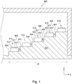
- As this type of semiconductor laser modules, there has heretofore been known a semiconductor laser module having a plurality of semiconductor laser devices mounted at different heights (see, e.g., Patent Literature 1). For example, as shown in
Fig. 1 , thissemiconductor laser module 900 includes a plurality ofsemiconductor laser devices 910 and astepped mount base 901 on which thosesemiconductor laser devices 910 are mounted. Each of thesemiconductor laser devices 910 includes asemiconductor chip 911 that emits a laser beam andelectrode pads 912 for supplying electric power to thesemiconductor chip 911. Themount base 901 includesmount surfaces 904 arranged at different heights for mounting a plurality ofsemiconductor laser devices 910 andstep side surfaces 905 that interconnect adjacent ones of themount surfaces 904. With this configuration, a plurality of laser beams can be emitted at different heights, and those laser beams can be condensed so as to output a high-power laser beam. - However, if distances G between the
electrode pads 912 and thestep side surfaces 905 are short in this configuration of thesemiconductor laser module 900, a dielectric breakdown may occur between theelectrode pads 912 and thestep side surfaces 905 when a voltage is applied to thesemiconductor laser module 900. Accordingly, in order to prevent a dielectric breakdown, the distances G need to be increased to some extent in thissemiconductor laser module 900. However, when the distances G are increased, the width L9 of themount base 901 problematically increases, resulting in an increased size of the module. - Patent Literature 1:
JP 2013-235943 A - The present invention has been made in view of the above drawbacks in the prior art. It is, therefore, a first object of the present invention to provide a semiconductor laser module that can achieve size reduction.
- It is a second object of the present invention to provide a method of manufacturing a semiconductor laser module that can achieve size reduction while generation of a dielectric breakdown is inhibited.
- According to a first aspect of the present invention, there is provided a semiconductor laser module that can achieve size reduction. This semiconductor laser module has an optical fiber that outputs a laser beam to an exterior of the semiconductor laser module and a plurality of semiconductor laser devices. Each of the plurality of semiconductor laser devices includes an emission portion that emits the laser beam, an electrically conductive portion that supplies electric power to the emission portion, and a mount on which the emission portion and the electrically conductive portion are mounted. The semiconductor laser module also has a mount base having a plurality of mount surfaces on which the mounts of the plurality of semiconductor laser devices are mounted and an optical system that optically couples the laser beams from the emission portions to an incident end face of the optical fiber, wherein the plurality of mount surfaces are formed in a stepped manner. The plurality of semiconductor laser devices include an upper semiconductor laser device and a lower semiconductor laser device disposed adjacent to each other in a step direction of the mount base. A portion of the upper semiconductor laser device protrudes from the mount surface toward the lower semiconductor laser device.
- According to such a semiconductor laser module, since a portion of the upper semiconductor laser device protrudes from the mount surface toward the lower semiconductor laser device, a distance between the lower semiconductor laser device and the upper semiconductor laser device is shortened. As a result, the mount base can be reduced in size, and hence the semiconductor laser module can be reduced in size.
- According to the present invention, the semiconductor laser module is thus reduced in size. Therefore, the optical path length of a laser beam emitted from the semiconductor laser device that is located farthest from the incident end face of the optical fiber (i.e., the maximum optical path length) is shortened.
- Meanwhile, the laser beam emitted from each of the semiconductor laser devices is collimated by a collimator lens. In practice, the laser beam that has passed through the collimator lens does not form completely parallel light and has a slight angle of divergence due to aberration and the like. Therefore, if the maximum optical path length increases, the "overall beam diameter" of a flux of laser beams from a plurality of semiconductor laser devices (overall laser beam) increases before the beam condensation. Thus, the overall beam diameter of the overall laser beam (spot diameter) also increases after the beam condensation. Accordingly, a portion of a laser beam component of the overall laser beam leaks out of a core of the optical fiber, resulting in coupling loss. In order to address such problems, it is conceivable that the curvature of a condenser lens is decreased to reduce the spot diameter. In such a case, a condensation angle of the condenser lens increases, so that coupling loss is caused by laser beam components that exceed the numerical aperture (NA) within which the optical fiber can receive light. As described above, as the maximum optical path length becomes longer, the coupling loss of the laser beam to the optical fiber increases.
- In contrast, according to the semiconductor laser module of the present invention, the maximum optical path length is shortened as described above. Accordingly, the coupling efficiency of the laser beam to the optical fiber can be improved.
- Preferably, an inhibition space is formed below the portion of the upper semiconductor laser device for inhibiting a dielectric breakdown from occurring between the mount base and the electrically conductive portion of the lower semiconductor laser device. The inhibition space may be formed such that the shortest separation distance from the mount base to the electrically conductive portion of the lower semiconductor laser device in the inhibition space is more than or equal to an inhibition distance with which a dielectric breakdown is inhibited from occurring between the electrically conductive portion and the mount base.
- In this case, the inhibition distance Lc (mm) may be calculated by

- Furthermore, when the inhibition space is formed by air, the inhibition distance Lc may be calculated by

- This configuration simultaneously achieves size reduction of the semiconductor laser module, improvement in coupling efficiency due to the size reduction, and inhibition of a dielectric breakdown in the module.
- The mount surface of the mount base preferably extends to at least a location right below the emission portion of the semiconductor laser device mounted on the mount surface. This configuration allows heat generated in the emission portion to be radiated to the mount base through the mount surface. Accordingly, the efficiency of heat dissipation of the semiconductor laser module is increased.
- Preferably, the mount base further has a positioning structure that allows the plurality of semiconductor laser devices to be positioned such that the inhibition space is formed. This configuration facilitates formation of the inhibition space. For example, such a positioning structure includes a protrusion portion projecting upward from the mount surface so that the mount abuts on the protrusion portion. The mount base may have an inclination surface extending obliquely upward from the mount surface, and a boundary between the mount surface and the inclination surface may be used for the positioning structure.
- According to a second aspect of the present invention, there is provided a method of manufacturing a semiconductor laser module that can achieve size reduction while generation of a dielectric breakdown is inhibited. In this manufacturing method, a mount base having a plurality of mount surfaces including an upper mount surface and a lower mount surface located adjacent to each other in a step direction is first prepared, wherein the plurality of mount surfaces are formed in a stepped manner. An upper semiconductor laser device to be mounted on the upper mount surface and a lower semiconductor laser device to be mounted on the lower mount surface are prepared. Then the lower semiconductor laser device is placed and fixed onto the lower mount surface so that an inhibition space is formed between the mount base and an electrically conductive portion of the lower semiconductor laser device for inhibiting a dielectric breakdown from occurring between the electrically conductive portion and the mount base. The upper semiconductor laser device is placed and fixed onto the upper mount surface so that a portion of the upper semiconductor laser device protrudes from the upper mount surface toward the lower semiconductor laser device.
- In the above manufacturing method, a positioning structure may be provided on the plurality of mount surfaces for positioning the plurality of semiconductor laser devices so that the inhibition space is formed. This configuration allows the semiconductor laser device to abut on the positioning structure. Accordingly, the inhibition space can readily be formed.
- After the upper semiconductor laser device is placed on the upper mount surface and the lower semiconductor laser device is placed on the lower mount surface, the mount base may be inclined so as to bring the upper semiconductor laser device and the lower semiconductor laser device into abutment on the positioning structure. While the abutment state is maintained, the upper semiconductor laser device and the lower semiconductor laser device may be fixed to the plurality of mount surfaces. This configuration allows a plurality of semiconductor laser devices to be positioned collectively and also to be fixed to the mount base simultaneously. Accordingly, a semiconductor laser module that can achieve size reduction while generation of a dielectric breakdown is inhibited can more readily be manufactured.
- According to the present invention, since a portion of the upper semiconductor laser device protrudes from the mount surface toward the lower semiconductor laser device, a distance between the upper semiconductor laser device and the lower semiconductor laser device is shortened, so that size reduction of the semiconductor laser module can be achieved.
-
-
Fig. 1 is a partial cross-sectional view showing a conventional semiconductor laser module. -
Fig. 2 is a partially cross-sectional plan view showing a semiconductor laser module according to a first embodiment of the present invention. -
Fig. 3 is a partially cross-sectional view taken along line A-A ofFig. 2 , which shows only the vicinity of a mount base of the semiconductor laser module illustrated inFig. 1 . -
Fig. 4 is an enlarged cross-sectional view showing a portion of the mount base illustrated inFig. 3 . -
Fig. 5 is a cross-sectional view showing a semiconductor laser module according to a second embodiment of the present invention, which corresponds toFig. 3 . -
Fig. 6 is a view showing a portion of a mount base of the semiconductor laser module illustrated inFig. 5 . -
Fig. 7 is a diagram showing a manufacturing method of the semiconductor laser module illustrated inFig. 2 . -
Fig. 8 is a diagram showing a manufacturing method of the semiconductor laser module illustrated inFig. 2 . - Embodiments of a semiconductor laser module according to the present invention will be described in detail below with reference to
Figs. 2 to 8 . InFigs. 2 to 8 , the same or corresponding components are denoted by the same or corresponding reference numerals and will not be described below repetitively. Furthermore, inFigs. 2 to 8 , the scales or dimensions of components may be exaggerated, or some components may be omitted. -
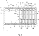
Fig. 2 is a partially cross-sectional plan view showing asemiconductor laser module 1 according to a first embodiment of the present invention, andFig. 3 is a partially cross-sectional view taken along line A-A ofFig. 2 , which shows only the vicinity of amount base 20 of thesemiconductor laser module 1. - As shown in
Figs. 2 and3 , thesemiconductor laser module 1 has a plurality ofsemiconductor laser devices 30A-30E (five semiconductor laser devices in this embodiment), fast-axis collimator lenses 40 and slow-axis collimator lenses 41, which are provided so as to correspond to the respectivesemiconductor laser devices 30A-30E, reflection mirrors 42 that reflect laser beams from thesemiconductor laser devices 30A-30E, acondenser lens 43 that condenses a plurality of laser beams reflected on the reflection mirrors 42, anoptical fiber 44 that outputs a laser beam condensed by thecondenser lens 43 to an exterior of thesemiconductor laser module 1, and ahousing 10 that houses the semiconductor laser devices, the lenses, and the mirrors therein. InFig. 3 , for the sake of clarity, the slow-axis collimator lenses 41, the reflection mirrors 42, and the like are omitted from the illustration. - As shown in
Figs. 2 and3 , thehousing 10 includes abottom plate 12 having a generally rectangular shape with longitudinal sides extending along the X-direction, aframe 11 fixed to a peripheral portion of thebottom plate 12, and acover body 16 fixed to a surface of theframe 11 on the +Z side. In the present embodiment, thebottom plate 12 is formed of a metal having a good thermal conductivity (e.g., copper). Theframe 11 and thecover body 16 are formed integrally with each other to constitute acover member 15. - Hereinafter, the +Z side, i.e., the side that is relatively farther from the
bottom plate 12, may be referred to as "upper," "upward," or "upper side." The -Z side, i.e., the side that is relatively closer to thebottom plate 12, may be referred to as "lower," "downward," or "lower side." - As shown in
Fig. 2 , theoptical fiber 44 is provided on the -X side of thebottom plate 12 and in the vicinity of an end of thebottom plate 12 along the +Y-direction. Thisoptical fiber 44 is fixed to afiber mount 45 mounted on thebottom plate 12 by, for example,solder 46. Theoptical fiber 44 extends to an exterior of thesemiconductor laser module 1 through awall 11A of theframe 11 of thehousing 10 on the -X side. - As shown in
Figs. 2 and3 , amount base 20 is formed over a substantially right half of the bottom plate 12 (+X side). The height of themount base 20 increases in a stepped manner toward the +X-direction. Thismount base 20 includes fivemount surfaces 21A-21E, which are parallel to the XY-plane. More specifically, as shown inFig. 3 , themount base 20 includes amount surface 21A that is located at the lowermost position in height from thebottom plate 12 along the Z-direction (step direction), amount surface 21B located adjacent to and on an upper side of themount surface 21A, amount surface 21C located adjacent to and on an upper side of themount surface 21B, amount surface 21D located adjacent to and on an upper side of themount surface 21C, and amount surface 21E located adjacent to and on an upper side of themount surface 21D. - Hereinafter, the +X side may be referred to as "right," or "right side," whereas the -X side may be referred to as "left," or "left side."
- As shown in
Fig. 2 , one of thesemiconductor laser devices 30A-30E, the fast-axis collimator lens 40, the slow-axis collimator lens 41, and thereflection mirror 42 are arranged from the -Y side to the +Y side and fixed on each of the mount surfaces 21A-21E (for example, thesemiconductor laser device 30A is fixed on themount surface 21A, and thesemiconductor laser device 30C is fixed on themount surface 21C). - As shown in
Fig. 3 , each of thesemiconductor laser devices 30A-30E includes a semiconductor chip 31 (emission portion) that emits a laser beam, a pair of electrode pads for supplying electric power to the semiconductor chip 31 (i.e., a left electrode pad 32 (electrically conductive portion) located on the left side of thesemiconductor chip 31 and a right electrode pad 33 (electrically conductive portion) located on the right side of the semiconductor chip 31), and amount 34 on which thesemiconductor chip 31 and theelectrode pads mount 34 is formed of a material having good insulation properties. In the present embodiment, themount 34 is formed of aluminum nitride. - The direction perpendicular to the pn junction of a semiconductor laser device is referred to as a fast axis, and the direction parallel to the pn junction of the semiconductor laser device is referred to as a slow axis. The degree of divergence of light from a semiconductor laser device is much greater along the fast axis than that along the slow axis. Therefore, laser beams emitted from the
semiconductor laser devices 30A-30E widely spread along the fast axis. In the present embodiment, the fast axis of the laser beams emitted from thesemiconductor laser devices 30A-30E extends along the Z-direction ofFig. 3 , and the slow axis of the laser beams extends along the X-direction. Accordingly, as shown inFig. 2 , the fast-axis collimator lenses 40 are provided adjacent to thesemiconductor laser devices 30A-30E. Thus, each of the fast-axis collimator lenses 40 collimates a laser beam originating from the adjacent semiconductor laser device and spreading along the fast axis (Z-direction). Meanwhile, each of the slow-axis collimator lenses 41 is provided between the fast-axis collimator lens 40 and thereflection mirror 42 in the laser emission direction (Y-direction). Thus, the laser beams that have been collimated along the fast axis are further collimated along the slow axis (X-direction) by the slow-axis collimator lenses 41. - As shown in
Fig. 2 , the five reflection mirrors 42 are arranged on the +Y side of the slow-axis collimator lenses 41 along a line extending in the X-direction. Each of those reflection mirrors 42 is arranged so as to change the direction of a laser beam propagating along the +Y-direction by 90°. Therefore, each of the laser beams emitted from the semiconductor chips 31 and collimated by thecollimator lenses reflection mirror 42 located frontward, so that the direction of the laser beam changes into the -X-direction. Thus, a plurality of laser beams are introduced into thecondenser lens 43 at different positions in the Z-direction. - The
condenser lens 43 serves to condense the laser beams in the Y-direction and the Z-direction and has an optical axis extending along the X-direction. Thiscondenser lens 43 is optically aligned in the X-direction, the Y-direction, and the Z-direction and positioned with high precision in the X-direction, the Y-direction, and the Z-direction. Therefore, a plurality of laser beams that have passed through thecondenser lens 43 are positioned with high precision in the X-direction, the Y-direction, and the Z-direction and are thus condensed onto anend face 44A (incident end face 44A) of theoptical fiber 44 on the +X side. As a result, a plurality of laser beams condensed onto theincident end face 44A of theoptical fiber 44 are optically coupled to theincident end face 44A of theoptical fiber 44 and outputted to an exterior of thesemiconductor laser module 1 through theoptical fiber 44. - As described above, according to the
semiconductor laser module 1, laser beams from a plurality ofsemiconductor laser devices 30A-30E can be condensed onto theincident end face 44A of theoptical fiber 44 by using an optical system including thecollimator lenses condenser lens 43. Thus, an output of thesemiconductor laser module 1 can be increased. However, if an optical path length from thesemiconductor chip 31 to the incident end face 44A increases, then coupling loss may be caused on the incident end face 44A to exert adverse influence on the output of thesemiconductor laser module 1. The present invention is to solve such a problem in an effective manner by reducing the size of the semiconductor laser module. Now the features of the present invention will be described in detail. - As shown in
Fig. 3 , themount base 20, on which a plurality ofsemiconductor laser devices 30A-30E (fivesemiconductor laser devices 30A-30E) are mounted, has fivemount surfaces 21A-21E on which the semiconductor laser devices 30 are fixed andprotrusion portions 22A-22E projecting upward from right edges of the respective mount surfaces 21A-21E. - As shown in
Fig. 3 , astep side surface 23A extends upward from the right edge of theprotrusion portion 22A and connects to themount surface 21B, which is located at the second lowermost position. Similarly, astep side surface 23B extends upward from the right edge of theprotrusion portion 22B and connects to themount surface 21C, which is located at the third lowermost position, and astep side surface 23C extends upward from the right edge of theprotrusion portion 22C and connects to themount surface 21D, which is located at the fourth lowermost position. Astep side surface 23D extends upward from the right edge of theprotrusion portion 22D and connects to themount surface 21E, which is located at the fifth lowermost position. Furthermore, the right edge of theprotrusion portion 22E forms a portion of the right edge of themount base 20 and abuts on theframe 11 of thehousing 10. -
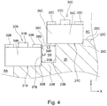
Fig. 4 is an enlarged cross-sectional view showing the vicinity of thesemiconductor laser devices Fig. 4 , thesemiconductor laser device 30B, which is mounted on themount surface 21B located at the second lowermost position, and thesemiconductor laser device 30C, which is mounted on themount surface 21C located adjacent to and on an upper side of themount surface 21B, are disposed adjacent to each other in the Z-direction (step direction). Specifically, thesemiconductor laser device 30B is referred to as a semiconductor laser device located on a relatively lower side in a pair ofsemiconductor laser devices semiconductor laser device 30C is referred to as a semiconductor laser device located on a relatively upper side in the pair ofsemiconductor laser devices - When an attention is directed to other pairs of semiconductor laser devices disposed adjacent to each other in the Z-direction, for example, when an attention is directed to a pair of
semiconductor laser devices Fig. 3 , thesemiconductor laser device 30C can be referred to as a lower semiconductor laser device, and thesemiconductor laser device 30D can be referred to as an upper semiconductor laser device. - As shown in
Fig. 4 , theprotrusion portion 22B has aside surface 26B that is parallel to the YZ-plane and abuts on themount 34B of the lowersemiconductor laser device 30B and anupper surface 25B that is parallel to the XY-plane and connects theside surface 26B and thestep side surface 23B to each other. Similarly, theprotrusion portion 22C has aside surface 26C that is parallel to the YZ-plane and abuts on themount 34C of the uppersemiconductor laser device 30C and anupper surface 25C that is parallel to the XY-plane and connects theside surface 26C and thestep side surface 23C (seeFig. 3 ) to each other. - As shown in
Fig. 4 , themount 34C of the uppersemiconductor laser device 30C abuts theside surface 26C of theprotrusion portion 22C, so that themount 34C of the uppersemiconductor laser device 30C is positioned in the X-direction. The length of themount surface 21C as measured in the X-direction, i.e., the length from theside surface 26C to thestep side surface 23B as measured in the X-direction, is shorter than the length of themount 34C of the uppersemiconductor laser device 30C as measured in the X-direction. Therefore, aleft portion 35C of themount 34C protrudes from themount surface 21C by a certain distance. Thus, theprotrusion portion 22C serves as a positioning structure that allows the uppersemiconductor laser device 30C to be positioned so as to protrude from themount surface 21C. - Furthermore, as shown in
Fig. 4 , themount 34B of the lowersemiconductor laser device 30B abuts on theside surface 26B of theprotrusion portion 22B, so that themount 34B of the lowersemiconductor laser device 30B is positioned in the X-direction. More specifically, the lowersemiconductor laser device 30B is positioned such that aright side surface 38B of theright electrode pad 33B of the lowersemiconductor laser device 30B is spaced from thestep side surface 23B in the X-direction by a distance L2 and that a bottom 39B of theright side surface 38B is spaced from theupper surface 25B of theprotrusion portion 22B in the Z-direction by a distance L3. Thus, theprotrusion portion 22B serves as a positioning structure that allows the lowersemiconductor laser device 30B to be positioned as described above. - As shown in
Fig. 4 , the distance L2 is the shortest separation distance from theright electrode pad 33B of the lowersemiconductor laser device 30B to thestep side surface 23B (mount base 20). The distance L3 is the shortest separation distance from theright electrode pad 33B to theupper surface 25B (mount base 20) of theprotrusion portion 22B. - With the configuration described above, as shown in
Fig. 4 , a space SB is defined right below the uppersemiconductor laser device 30C (theleft portion 35C of themount 34C) by abottom surface 36C of theleft portion 35C, thestep side surface 23B, theupper surface 25B of theprotrusion portion 22B, aright side surface 37B of themount 34B of the lowersemiconductor laser device 30B, and theright side surface 38B of theright electrode pad 33B of the lowersemiconductor laser device 30B. Theleft portion 35C of themount 34C of the uppersemiconductor laser device 30C protrudes above the space SB. In other words, theleft portion 35C as a portion of the uppersemiconductor laser device 30C protrudes from themount surface 21C toward the lowersemiconductor laser device 30B. - As shown in
Fig. 3 , spaces SA, SC, and SD are formed right below the upper semiconductor laser devices in the other pairs of semiconductor laser devices. Portions of thesemiconductor laser devices - As described above, since a portion of each of a plurality of upper semiconductor laser devices protrudes above the space SA-SD (i.e., it protrudes toward the lower semiconductor laser device), the separation distance between the upper semiconductor laser device and the lower semiconductor laser device as measured in the X-direction is reduced as compared to that of the conventional semiconductor laser module 900 (see
Fig. 1 ). Thus, according to the present embodiment, the width L1 of the mount base 20 (seeFig. 3 ) is smaller than the width L9 of themount base 901 of the conventional semiconductor laser module 900 (seeFig. 1 ). Accordingly, the semiconductor laser module can be reduced in size. - The size reduction of the semiconductor laser module shortens an optical path length of the laser beam from the
semiconductor laser device 30E that is located farthest from theincident end face 44A (maximum optical path length) as compared to that of the conventional semiconductor laser module (seeFig. 1 ). Therefore, the coupling efficiency of the laser beam to the optical fiber can be improved, so that the output of the semiconductor laser module can effectively be increased. - Meanwhile, referring again to
Fig. 4 , if a certain distance is not maintained between thestep side surface 23B and theright electrode pad 33B of the lowersemiconductor laser device 30B, then a dielectric breakdown may occur between theright electrode pad 33B and thestep side surface 23B of themount base 20. Accordingly, in the present embodiment, the shortest separation distance L2 between theright electrode pad 33B and thestep side surface 23B is set to be more than or equal to an inhibition distance with which a dielectric breakdown is inhibited from occurring between theright electrode pad 33B and thestep side surface 23B. - Similarly, if a certain distance is not maintained between the
upper surface 25B of theprotrusion portion 22B and theright electrode pad 33B, then a dielectric breakdown may occur between theright electrode pad 33B and theupper surface 25B of themount base 20. Accordingly, in the present embodiment, the shortest separation distance L3 between theright electrode pad 33B and theupper surface 25B is set to be more than or equal to an inhibition distance with which a dielectric breakdown is inhibited from occurring between theright electrode pad 33B and theupper surface 25B. - For example, such an inhibition distance Lc can be calculated by the following formula. Specifically, the inhibition distance Lc (mm) is calculated by

semiconductor laser module 1, and R (kV/mm) is an insulation resistance of the space SB (a voltage with which a dielectric breakdown occurs). - When the space SB is formed by air, the inhibition distance can be calculated by

- As a matter of course, the inhibition distance may be calculated by other formulas.
- In the present embodiment, the distances L2 and L3 are the same and are more than or equal to the inhibition distance Lc calculated by the formula (1) or (2). Accordingly, the space SB serves as an inhibition space for inhibiting a dielectric breakdown from occurring between the
right electrode pad 33B and thestep side surface 23B and for inhibiting a dielectric breakdown from occurring between theright electrode pad 33B and theupper surface 25B of theprotrusion portion 22B. In other words, the space SB serves as an inhibition space for inhibiting a dielectric breakdown from occurring between theright electrode pad 33B and themount base 20. - As shown in
Fig. 3 , the spaces SA, SC, and SD located right below the upper semiconductor laser devices in the other pairs of semiconductor laser devices serve as inhibition spaces with a similar configuration to the space SB. Thesemiconductor laser device 30E, which is located at the uppermost position, is positioned in the X-direction by theprotrusion portion 22E. Thus, a space SE formed between thesemiconductor laser device 30E and theframe 11 serves as an inhibition space. - As described above, according to the
semiconductor laser module 1 of the present embodiment, the inhibition spaces SA-SD are formed between the lower semiconductor laser devices and the step side surfaces (mount base) located adjacent to the lower semiconductor laser devices on the +X side. Accordingly, a dielectric breakdown is inhibited from occurring between the mount base and the electrode pads (seeFig. 3 ). - In this manner, according to the
semiconductor laser module 1 of the present embodiment, size reduction and increased output of the semiconductor laser module can be achieved while a dielectric breakdown is inhibited from occurring between the mount base and the semiconductor laser devices. - As shown in
Fig. 4 , themount surface 21C on which the uppersemiconductor laser device 30C is mounted preferably extends to at least a location right below thesemiconductor chip 31C of the uppersemiconductor laser device 30C. This configuration allows heat generated in thesemiconductor chip 31C to be radiated to the mount base 20 (copper) through themount surface 21C located right below thesemiconductor chip 31C. Accordingly, heat dissipation of thesemiconductor laser module 1 can be performed effectively. This holds true for the mount surfaces 21B, 21D, and 21E. - Furthermore, the positioning structure is not limited to the protrusion portion as described in the first embodiment and may be configured by a second embodiment as described below.
Fig. 5 is a cross-sectional view showing asemiconductor laser module 100 according to a second embodiment of the present invention, which corresponds toFig. 3 . - As shown in
Fig. 5 , thesemiconductor laser module 100 hassemiconductor laser devices 30A-30E and ahousing 110 that houses thesemiconductor laser devices 30A-30E and the like. Thehousing 110 includes abottom plate 112 having a generally rectangular shape with longitudinal sides extending along the X-direction and acover member 15 fixed to a peripheral portion of thebottom plate 112. Thebottom plate 112 is formed of copper as with the first embodiment. - A
mount base 120 is formed over a substantially right half of thebottom plate 112. The height of themount base 120 increases in a stepped manner toward the +X-direction. Thismount base 120 includes fivemount surfaces 21A-21E, which are parallel to the XY-plane. One of thesemiconductor laser devices 30A-30E, a fast-axis collimator lens 40, a slow-axis collimator lens 41, and areflection mirror 42 are fixed on each of the mount surfaces 21A-21E (seeFig. 2 ). - As shown in
Fig. 5 , themount base 120 includes fivemount surfaces 21A-21E on which thesemiconductor laser devices 30A-30E are fixed and inclination surfaces 123A-123E extending obliquely upward from respectiveright edges 122A-122E of the mount surfaces 21A-21E to the right side. More specifically, themount base 120 includes aninclination surface 123A extending obliquely upward from aright edge 122A of themount surface 21A to the right side, aninclination surface 123B extending obliquely upward from aright edge 122B of themount surface 21B to the right side, aninclination surface 123C extending obliquely upward from aright edge 122C of themount surface 21C to the right side, aninclination surface 123D extending obliquely upward from aright edge 122D of themount surface 21D to the right side, and aninclination surface 123E extending obliquely upward from aright edge 122E of themount surface 21E to the right side. - The
inclination surface 123A connects to a left edge of themount surface 21B that is located at the second lowermost position. Theinclination surface 123B connects to a left edge of themount surface 21C that is located at the third lowermost position. Theinclination surface 123C connects to a left edge of themount surface 21D that is located at the fourth lowermost position. Theinclination surface 123D connects to a left edge of themount surface 21E that is located at the uppermost position. Theinclination surface 123E extends to theframe 11, which is located adjacent to theinclination surface 123E. -
Fig. 6 is an enlarged view showing the vicinity of thesemiconductor laser device 30B (lower semiconductor laser device), which is mounted on the secondlowermost mount surface 21B, and thesemiconductor laser device 30C (upper semiconductor laser device), which is mounted on themount surface 21C located adjacent to and on an upper side of themount surface 21B. - As shown in
Fig. 6 , themount 34C of the uppersemiconductor laser device 30C is positioned in the X-direction by theright edge 122C of themount surface 21C (i.e., theboundary 122C between themount surface 21C and theinclination surface 123C). The length of themount surface 21C as measured in the X-direction, i.e., the length from theboundary 122C to theleft edge 128C, is shorter than the length of themount 34C as measured in the X-direction. Therefore, aleft portion 35C of themount 34C protrudes from themount surface 21C by a certain distance. Thus, theboundary 122C serves as a positioning structure that allows a portion (leftportion 35C) of the uppersemiconductor laser device 30C to be positioned so as to protrude from themount surface 21C. - Furthermore, as shown in
Fig. 6 , the lowersemiconductor laser device 30B (mount 34B) is positioned in the X-direction by theright edge 122B of themount surface 21B (i.e., theboundary 122B between themount surface 21B and theinclination surface 123B). More specifically, the lowersemiconductor laser device 30B is positioned such that the bottom 39B of theright side surface 38B of theright electrode pad 33B is spaced from theinclination surface 123B by a distance L4 as measured along a perpendicular line to theinclination surface 123B and that the bottom 39B is spaced from theboundary 122B in the Z-direction by a distance L5. Thus, theboundary 122B serves as a positioning structure that allows the lowersemiconductor laser device 30B to be positioned as described above. - As shown in
Fig. 6 , the distance L4 is the shortest separation distance from theright electrode pad 33B of the lowersemiconductor laser device 30B to theinclination surface 123B. The distance L5 is the shortest separation distance from theright electrode pad 33B to theboundary 122B. - With the configuration described above, as shown in
Fig. 6 , a space SB is defined right below the uppersemiconductor laser device 30C (theleft portion 35C of themount 34C) by thebottom surface 25C of theleft portion 35C, theinclination surface 123B, theright side surface 37B of themount 34B of the lowersemiconductor laser device 30B, and theright side surface 38B of theright electrode pad 33B of the lowersemiconductor laser device 30B. - In the present embodiment, the shortest separation distance L4 is set to be more than or equal to a length with which a dielectric breakdown is inhibited from occurring between the
right electrode pad 33B and theinclination surface 123B, i.e., an inhibition distance Lc calculated from the aforementioned formula (1) or (2). Furthermore, as shown inFig. 6 , the shortest separation distance L5 is longer than the shortest separation distance L4. - Accordingly, the space SB serves as an inhibition space for inhibiting a dielectric breakdown from occurring between the
right electrode pad 33B and theinclination surface 123B and for inhibiting a dielectric breakdown from occurring between theright electrode pad 33B and theboundary 122B. As shown inFig. 6 , according to the present embodiment, such an inhibition space SB is formed right below the uppersemiconductor laser device 30C. - As shown in
Fig. 5 , the spaces SA, SC, and SD also serve as inhibition spaces as with the space SB. Those spaces are formed right below the respective upper semiconductor laser devices. Thus, portions of the upper semiconductor laser devices protrude above the spaces SA, SC, and SD. Thesemiconductor laser device 30E is positioned by theboundary 122E. A space SE formed between theright electrode pad 33 of thesemiconductor laser device 30E and theframe 11 serves as an inhibition space. - With the aforementioned configuration, the width L6 of the mount base 120 (see
Fig. 5 ) can be made smaller than the width L9 of themount base 901 of the semiconductor laser module 900 (seeFig. 1 ) as with the first embodiment. Accordingly, the semiconductor laser module can be reduced in size. Thus, the second embodiment of the present invention also provides a small-sized, high-power semiconductor laser module in which a dielectric breakdown is unlikely to occur. - The positioning structures described in the aforementioned first and second embodiments may be used simultaneously. Alternatively, other positioning structures may be used. Rather, such positioning structures may not necessarily be provided in the mount base. Provision of a positioning structure facilitates production of a semiconductor laser module that can achieve both of size reduction and inhibition of a dielectric breakdown. This feature will be described below with an example in which a
semiconductor laser module 1 is manufactured. - In order to manufacture a
semiconductor laser module 1, as shown inFig. 7 , abottom plate 12 having amount base 20 formed thereon is prepared in the first place.Protrusion portions 22A-22E are formed as the aforementioned positioning structures in themount base 20. Then, as shown inFig. 7 , asolder sheet 70 is formed over a certain area of themount surface 21A that is adjacent to theprotrusion portion 22A. More specifically, thesolder sheet 70 is formed over an area sufficient to bond themount 34 of thesemiconductor laser device 30A to themount surface 21A.Solder sheets 70 are also formed on the mount surfaces 21B-21E as with themount surface 21A. Thereafter, as shown inFig. 7 , thesemiconductor laser devices 30A-30E are respectively placed on the mount surfaces 21A-21E on which thesolder sheets 70 have been formed. - After placement of the
semiconductor laser devices 30A-30E, as shown inFig. 8 , thebottom plate 12 is inclined downward on the right side. This operation causes thesemiconductor laser devices 30A-30E to move obliquely downward to the right side on the inclined mount surfaces 21A-21E, so that therespective mounts 34 abut on the left side surfaces of theprotrusion portions 22A-22E. Thus, thesemiconductor laser devices 30A-30E are positioned in a collective manner. As show inFig. 8 , while this state is maintained, thebottom plate 12 is heated to melt thesolder sheets 70. In this manner, thesemiconductor laser devices 30A-30E are collectively solder-bonded to themount base 20. Finally, a cover member 15 (seeFigs. 2 and3 ) is fixed to a peripheral portion of thebottom plate 12. Thus, thesemiconductor laser module 1 is completed. - As described above, according to a manufacturing method of the present embodiment, provision of the
protrusion portions 22A-22E in themount base 20 allows thesemiconductor laser devices 30A-30E to be positioned in a collective manner merely by inclination of themount base 20. In this state, thesemiconductor laser devices 30A-30E can be bonded collectively to themount base 20 by heating thebottom plate 12. Accordingly, a small-sized, high-power semiconductor laser module in which a dielectric breakdown is unlikely to occur can readily be manufactured. - In the above manufacturing method, the bottom plate (mount base) may not necessarily be inclined. Even of the mount base is inclined, the provision of the positioning structures (protrusion portions) allows the semiconductor laser devices to abut on the positioning structures so that the semiconductor laser devices can be positioned. Accordingly, an inhibition space can readily be formed.
- From the viewpoint of manufacturing a small-sized, high-power semiconductor laser module in which a dielectric breakdown is unlikely to occur, even the positioning structure may not necessarily be provided on the mount base. In this case, the lower semiconductor laser device is placed on and fixed (solder-bonded) to a mount surface (lower mount surface) on which the lower semiconductor laser device is mounted, such that an inhibition space is formed between the mount base and the electrically conductive portion of the lower semiconductor laser device. The upper semiconductor laser device is fixed (solder-bonded) to a mount surface (upper mount surface) on which the upper semiconductor laser device is mounted, such that a portion of the upper semiconductor laser device protrudes from the upper mount surface toward the lower semiconductor laser device.
- As a matter of course, the above manufacturing method can be applied to the
semiconductor laser module 100 and any semiconductor laser module having other positioning structures. - Although some preferred embodiments of the present invention have been described, the present invention is not limited to the aforementioned embodiments. It should be understood that various different forms may be applied to the present invention within the technical idea thereof.
- The terms "below," "above," "bottom," "upward," "downward," "upper," "lower," and other positional terms described herein are used in connection with the illustrated embodiments and may be varied depending on the relative positional relationship between components of the apparatus.
- This application claims the benefit of priority from
Japanese patent application No. 2018-000069 - The present invention is suitably used for a semiconductor laser module having a plurality of semiconductor laser devices.
-
- 1, 100
- Semiconductor laser module
- 10, 110
- Housing
- 11
- Frame
- 12, 112
- Bottom plate
- 15
- Cover member
- 16
- Cover body
- 20, 120
- Mount base
- 21A-21E
- Mount surface
- 22A-22E
- Protrusion portion (positioning structure)
- 23A-23D
- Step side surface
- 30A-30E
- Semiconductor laser device
- 31
- Semiconductor chip (emission portion)
- 32
- Left electrode pad (electrically conductive portion)
- 33
- Right electrode pad (electrically conductive portion)
- 34
- Mount
- 40
- Fast-axis collimator lens (optical system)
- 41
- Slow-axis collimator lens (optical system)
- 42
- Reflection mirror (optical system)
- 43
- Condenser lens (optical system)
- 44
- Optical fiber
- 44A
- Incident end face
- 45
- Fiber mount
- 46
- Solder
- 70
- Solder sheet
- 122B, 122C
- Boundary (positioning structure)
- 123A-123E
- Inclination surface
- SA-SE
- Inhibition space
Claims (12)
- A semiconductor laser module comprising:an optical fiber that outputs a laser beam to an exterior of the semiconductor laser module;a plurality of semiconductor laser devices each including an emission portion that emits the laser beam, an electrically conductive portion that supplies electric power to the emission portion, and a mount on which the emission portion and the electrically conductive portion are mounted;a mount base having a plurality of mount surfaces on which the mounts of the plurality of semiconductor laser devices are mounted, the plurality of mount surfaces being formed in a stepped manner; andan optical system that optically couples the laser beams from the emission portions to an incident end face of the optical fiber,wherein the plurality of semiconductor laser devices include an upper semiconductor laser device and a lower semiconductor laser device disposed adjacent to each other in a step direction of the mount base, anda portion of the upper semiconductor laser device protrudes from the mount surface toward the lower semiconductor laser device.
- The semiconductor laser module as recited in claim 1, wherein an inhibition space is formed below the portion of the upper semiconductor laser device for inhibiting a dielectric breakdown from occurring between the mount base and the electrically conductive portion of the lower semiconductor laser device.
- The semiconductor laser module as recited in claim 2, wherein the inhibition space is formed such that a shortest separation distance from the mount base to the electrically conductive portion of the lower semiconductor laser device in the inhibition space is more than or equal to an inhibition distance with which a dielectric breakdown is inhibited from occurring between the electrically conductive portion and the mount base.
- The semiconductor laser module as recited in claim 3, wherein the inhibition distance Lc (mm) is calculated by

- The semiconductor laser module as recited in claim 4, wherein the inhibition space is formed by air, and
the inhibition distance Lc is calculated by
- The semiconductor laser module as recited in any one of claims 2 to 5, wherein the mount base further has a positioning structure that allows the plurality of semiconductor laser devices to be positioned such that the inhibition space is formed.
- The semiconductor laser module as recited in claim 6, wherein the positioning structure includes a protrusion portion projecting upward from the mount surface so that the mount abuts on the protrusion portion.
- The semiconductor laser module as recited in claim 6 or 7, wherein the mount base has an inclination surface extending obliquely upward from the mount surface, and
the positioning structure includes a boundary between the mount surface and the inclination surface. - The semiconductor laser module as recited in any one of claims 1 to 8, wherein the mount surface of the mount base extends to at least a location right below the emission portion of the semiconductor laser device mounted on the mount surface.
- A method of manufacturing a semiconductor laser module, the method comprising:preparing a mount base having a plurality of mount surfaces including an upper mount surface and a lower mount surface located adjacent to each other in a step direction, the plurality of mount surfaces being formed in a stepped manner;preparing an upper semiconductor laser device to be mounted on the upper mount surface and a lower semiconductor laser device to be mounted on the lower mount surface;placing and fixing the lower semiconductor laser device onto the lower mount surface so that an inhibition space is formed between the mount base and an electrically conductive portion of the lower semiconductor laser device for inhibiting a dielectric breakdown from occurring between the electrically conductive portion and the mount base; andplacing and fixing the upper semiconductor laser device onto the upper mount surface so that a portion of the upper semiconductor laser device protrudes from the upper mount surface toward the lower semiconductor laser device.
- The method of manufacturing a semiconductor laser module as recited in claim 10, wherein a positioning structure is provided on the plurality of mount surfaces for positioning the plurality of semiconductor laser devices so that the inhibition space is formed.
- The method of manufacturing a semiconductor laser module as recited in claim 11, wherein, after placing the upper semiconductor laser device on the upper mount surface and placing the lower semiconductor laser device on the lower mount surface, the mount base is inclined so as to bring the upper semiconductor laser device and the lower semiconductor laser device into abutment on the positioning structure, and
while the abutment state is maintained, the upper semiconductor laser device and the lower semiconductor laser device are fixed to the plurality of mount surfaces.
Applications Claiming Priority (2)
| Application Number | Priority Date | Filing Date | Title |
|---|---|---|---|
| JP2018000069A JP6615238B2 (en) | 2018-01-04 | 2018-01-04 | Semiconductor laser module |
| PCT/JP2018/047911 WO2019135379A1 (en) | 2018-01-04 | 2018-12-26 | Semiconductor laser module and semiconductor laser module production method |
Publications (3)
| Publication Number | Publication Date |
|---|---|
| EP3736924A1 true EP3736924A1 (en) | 2020-11-11 |
| EP3736924A4 EP3736924A4 (en) | 2021-10-27 |
| EP3736924B1 EP3736924B1 (en) | 2024-01-31 |
Family
ID=67143645
Family Applications (1)
| Application Number | Title | Priority Date | Filing Date |
|---|---|---|---|
| EP18898328.2A Active EP3736924B1 (en) | 2018-01-04 | 2018-12-26 | Semiconductor laser module and method of manufacturing semiconductor laser module |
Country Status (5)
| Country | Link |
|---|---|
| US (1) | US11515689B2 (en) |
| EP (1) | EP3736924B1 (en) |
| JP (1) | JP6615238B2 (en) |
| CN (1) | CN111557066B (en) |
| WO (1) | WO2019135379A1 (en) |
Cited By (2)
| Publication number | Priority date | Publication date | Assignee | Title |
|---|---|---|---|---|
| US11557874B2 (en) * | 2021-05-18 | 2023-01-17 | Trumpf Photonics, Inc. | Double-sided cooling of laser diodes |
| US11876343B2 (en) | 2021-05-18 | 2024-01-16 | Trumpf Photonics, Inc. | Laser diode packaging platforms |
Families Citing this family (1)
| Publication number | Priority date | Publication date | Assignee | Title |
|---|---|---|---|---|
| JP2022069323A (en) * | 2020-10-23 | 2022-05-11 | 住友電気工業株式会社 | Optical device |
Family Cites Families (13)
| Publication number | Priority date | Publication date | Assignee | Title |
|---|---|---|---|---|
| JPS6063981A (en) * | 1984-07-27 | 1985-04-12 | Hitachi Ltd | Semiconductor light emitting device |
| JP3617116B2 (en) * | 1995-03-31 | 2005-02-02 | 住友電気工業株式会社 | Two-dimensional array type optical element module |
| US5987043A (en) * | 1997-11-12 | 1999-11-16 | Opto Power Corp. | Laser diode arrays with offset components |
| JP2000101182A (en) * | 1998-09-21 | 2000-04-07 | Sanyo Electric Co Ltd | Semiconductor laser |
| JP2004179607A (en) * | 2002-09-30 | 2004-06-24 | Fuji Photo Film Co Ltd | Laser device |
| US7724798B2 (en) | 2003-10-15 | 2010-05-25 | Sanyo Electric Co., Ltd. | Two-beam semiconductor laser apparatus |
| TWI340837B (en) * | 2007-08-01 | 2011-04-21 | Amtran Technology Co Ltd | Optical communication device |
| US7733932B2 (en) * | 2008-03-28 | 2010-06-08 | Victor Faybishenko | Laser diode assemblies |
| US8989530B2 (en) * | 2010-07-22 | 2015-03-24 | Avago Technologies General Ip (Singapore) Pte. Ltd. | Optoelectronic modules and submount for same and a method for manufacturing an array of optical devices |
| JP5730814B2 (en) * | 2012-05-08 | 2015-06-10 | 古河電気工業株式会社 | Semiconductor laser module |
| CN104112980A (en) | 2014-07-10 | 2014-10-22 | 北京凯普林光电科技有限公司 | Staggerly-laminated optical path module and multi-die semiconductor laser |
| US9413136B1 (en) * | 2015-07-08 | 2016-08-09 | Trumpf Photonics, Inc. | Stepped diode laser module with cooling structure |
| JP7002068B2 (en) | 2016-06-30 | 2022-01-20 | 日本製紙株式会社 | Ruminant breeding method |
-
2018
- 2018-01-04 JP JP2018000069A patent/JP6615238B2/en active Active
- 2018-12-26 EP EP18898328.2A patent/EP3736924B1/en active Active
- 2018-12-26 CN CN201880085252.5A patent/CN111557066B/en active Active
- 2018-12-26 WO PCT/JP2018/047911 patent/WO2019135379A1/en unknown
- 2018-12-26 US US16/958,355 patent/US11515689B2/en active Active
Cited By (2)
| Publication number | Priority date | Publication date | Assignee | Title |
|---|---|---|---|---|
| US11557874B2 (en) * | 2021-05-18 | 2023-01-17 | Trumpf Photonics, Inc. | Double-sided cooling of laser diodes |
| US11876343B2 (en) | 2021-05-18 | 2024-01-16 | Trumpf Photonics, Inc. | Laser diode packaging platforms |
Also Published As
| Publication number | Publication date |
|---|---|
| EP3736924B1 (en) | 2024-01-31 |
| EP3736924A4 (en) | 2021-10-27 |
| CN111557066B (en) | 2023-04-18 |
| WO2019135379A1 (en) | 2019-07-11 |
| US20210066891A1 (en) | 2021-03-04 |
| CN111557066A (en) | 2020-08-18 |
| JP2019121672A (en) | 2019-07-22 |
| JP6615238B2 (en) | 2019-12-04 |
| US11515689B2 (en) | 2022-11-29 |
Similar Documents
| Publication | Publication Date | Title |
|---|---|---|
| EP3736924B1 (en) | Semiconductor laser module and method of manufacturing semiconductor laser module | |
| US8475056B2 (en) | Semiconductor device assembly | |
| US7310457B2 (en) | Multi-chip module and method for mounting thereof | |
| EP2256880B1 (en) | Laser light source module | |
| CN107005022B (en) | Optical unit, fixing structure of optical unit, and semiconductor laser module | |
| JP6665666B2 (en) | Method for manufacturing light emitting device, method for manufacturing laser module, and light emitting device | |
| US11619365B2 (en) | Light source unit, illumination device, processing equipment, and deflection element | |
| US10522969B2 (en) | Light-emitting device and lid body used in light-emitting device | |
| US11432401B2 (en) | Electronic assembly and automotive luminous device | |
| JP2017069109A (en) | Light source device | |
| US11460166B2 (en) | Light emitting diode (LED) pad mount system | |
| JP5985899B2 (en) | Semiconductor laser device | |
| WO2016203789A1 (en) | Laser device and laser device manufacturing method | |
| JP3429190B2 (en) | Optical semiconductor device | |
| CN113467044A (en) | Reflector device and light source device having the same | |
| JP2001264590A (en) | Package for optical module | |
| JP2004146630A (en) | Optical module | |
| JP2019125726A (en) | Semiconductor laser module and manufacturing method thereof | |
| JP2000028870A (en) | Optical coupler | |
| JP2018170431A (en) | Semiconductor laser device and manufacturing method for the same | |
| US20220329041A1 (en) | Laser Engine Supporting Multiple Laser Sources | |
| EP3805833A1 (en) | Lighting device and method for manufacturing a lighting device | |
| JP2019053230A (en) | Optical module and manufacturing method thereof | |
| JP2020181997A (en) | Light-emitting module | |
| JP2019020623A (en) | Square lens component, and optical module using the same and manufacturing method thereof |
Legal Events
| Date | Code | Title | Description |
|---|---|---|---|
| STAA | Information on the status of an ep patent application or granted ep patent |
Free format text: STATUS: THE INTERNATIONAL PUBLICATION HAS BEEN MADE |
|
| PUAI | Public reference made under article 153(3) epc to a published international application that has entered the european phase |
Free format text: ORIGINAL CODE: 0009012 |
|
| STAA | Information on the status of an ep patent application or granted ep patent |
Free format text: STATUS: REQUEST FOR EXAMINATION WAS MADE |
|
| 17P | Request for examination filed |
Effective date: 20200803 |
|
| AK | Designated contracting states |
Kind code of ref document: A1 Designated state(s): AL AT BE BG CH CY CZ DE DK EE ES FI FR GB GR HR HU IE IS IT LI LT LU LV MC MK MT NL NO PL PT RO RS SE SI SK SM TR |
|
| AX | Request for extension of the european patent |
Extension state: BA ME |
|
| DAV | Request for validation of the european patent (deleted) | ||
| DAX | Request for extension of the european patent (deleted) | ||
| A4 | Supplementary search report drawn up and despatched |
Effective date: 20210928 |
|
| RIC1 | Information provided on ipc code assigned before grant |
Ipc: H01S 5/02375 20210101ALI20210922BHEP Ipc: H01S 5/02326 20210101ALI20210922BHEP Ipc: H01S 5/0233 20210101ALI20210922BHEP Ipc: H01S 5/02325 20210101ALI20210922BHEP Ipc: H01S 5/022 20210101ALI20210922BHEP Ipc: G02B 6/42 20060101ALI20210922BHEP Ipc: H01S 5/40 20060101AFI20210922BHEP |
|
| RIC1 | Information provided on ipc code assigned before grant |
Ipc: H01S 5/0239 20210101ALI20230908BHEP Ipc: H01S 5/024 20060101ALI20230908BHEP Ipc: H01S 5/02375 20210101ALI20230908BHEP Ipc: H01S 5/02326 20210101ALI20230908BHEP Ipc: H01S 5/0233 20210101ALI20230908BHEP Ipc: H01S 5/02325 20210101ALI20230908BHEP Ipc: H01S 5/022 20060101ALI20230908BHEP Ipc: G02B 6/42 20060101ALI20230908BHEP Ipc: H01S 5/40 20060101AFI20230908BHEP |
|
| GRAP | Despatch of communication of intention to grant a patent |
Free format text: ORIGINAL CODE: EPIDOSNIGR1 |
|
| STAA | Information on the status of an ep patent application or granted ep patent |
Free format text: STATUS: GRANT OF PATENT IS INTENDED |
|
| RIN1 | Information on inventor provided before grant (corrected) |
Inventor name: KASAI, YOHEI Inventor name: KATAGIRI, KEN |
|
| INTG | Intention to grant announced |
Effective date: 20231102 |
|
| GRAS | Grant fee paid |
Free format text: ORIGINAL CODE: EPIDOSNIGR3 |
|
| GRAA | (expected) grant |
Free format text: ORIGINAL CODE: 0009210 |
|
| STAA | Information on the status of an ep patent application or granted ep patent |
Free format text: STATUS: THE PATENT HAS BEEN GRANTED |
|
| AK | Designated contracting states |
Kind code of ref document: B1 Designated state(s): AL AT BE BG CH CY CZ DE DK EE ES FI FR GB GR HR HU IE IS IT LI LT LU LV MC MK MT NL NO PL PT RO RS SE SI SK SM TR |
|
| REG | Reference to a national code |
Ref country code: GB Ref legal event code: FG4D Ref country code: CH Ref legal event code: EP |
|
| REG | Reference to a national code |
Ref country code: DE Ref legal event code: R096 Ref document number: 602018064832 Country of ref document: DE |
|
| REG | Reference to a national code |
Ref country code: IE Ref legal event code: FG4D |