EP3736618A1 - Antenne à cristaux liquides plate et son procédé de fabrication - Google Patents
Antenne à cristaux liquides plate et son procédé de fabrication Download PDFInfo
- Publication number
- EP3736618A1 EP3736618A1 EP19863988.2A EP19863988A EP3736618A1 EP 3736618 A1 EP3736618 A1 EP 3736618A1 EP 19863988 A EP19863988 A EP 19863988A EP 3736618 A1 EP3736618 A1 EP 3736618A1
- Authority
- EP
- European Patent Office
- Prior art keywords
- metal film
- film layer
- substrate
- liquid crystal
- patterned
- Prior art date
- Legal status (The legal status is an assumption and is not a legal conclusion. Google has not performed a legal analysis and makes no representation as to the accuracy of the status listed.)
- Pending
Links
- 239000004973 liquid crystal related substance Substances 0.000 title claims abstract description 81
- 238000004519 manufacturing process Methods 0.000 title claims abstract description 38
- 229910052751 metal Inorganic materials 0.000 claims abstract description 236
- 239000002184 metal Substances 0.000 claims abstract description 236
- 239000000758 substrate Substances 0.000 claims abstract description 131
- 238000000059 patterning Methods 0.000 claims abstract description 32
- 210000002858 crystal cell Anatomy 0.000 claims abstract description 9
- 229920002120 photoresistant polymer Polymers 0.000 claims description 62
- 238000005530 etching Methods 0.000 claims description 40
- 239000000463 material Substances 0.000 claims description 20
- 238000000576 coating method Methods 0.000 claims description 11
- RYGMFSIKBFXOCR-UHFFFAOYSA-N Copper Chemical group [Cu] RYGMFSIKBFXOCR-UHFFFAOYSA-N 0.000 claims description 10
- 239000011248 coating agent Substances 0.000 claims description 10
- 229910052802 copper Inorganic materials 0.000 claims description 10
- 239000010949 copper Substances 0.000 claims description 10
- 230000005855 radiation Effects 0.000 claims description 9
- 230000000717 retained effect Effects 0.000 claims description 8
- 239000007788 liquid Substances 0.000 claims description 7
- 239000011521 glass Substances 0.000 claims description 4
- 238000000034 method Methods 0.000 abstract description 34
- 230000006872 improvement Effects 0.000 abstract description 4
- 230000008569 process Effects 0.000 description 27
- 239000004020 conductor Substances 0.000 description 10
- 239000007769 metal material Substances 0.000 description 10
- 239000000565 sealant Substances 0.000 description 8
- 230000002500 effect on skin Effects 0.000 description 7
- 229910052782 aluminium Inorganic materials 0.000 description 5
- XAGFODPZIPBFFR-UHFFFAOYSA-N aluminium Chemical compound [Al] XAGFODPZIPBFFR-UHFFFAOYSA-N 0.000 description 5
- PCHJSUWPFVWCPO-UHFFFAOYSA-N gold Chemical compound [Au] PCHJSUWPFVWCPO-UHFFFAOYSA-N 0.000 description 5
- 229910052737 gold Inorganic materials 0.000 description 5
- 239000010931 gold Substances 0.000 description 5
- 229910052709 silver Inorganic materials 0.000 description 5
- 239000004332 silver Substances 0.000 description 5
- BQCADISMDOOEFD-UHFFFAOYSA-N Silver Chemical compound [Ag] BQCADISMDOOEFD-UHFFFAOYSA-N 0.000 description 4
- 238000004891 communication Methods 0.000 description 4
- 238000005516 engineering process Methods 0.000 description 4
- 229910045601 alloy Inorganic materials 0.000 description 3
- 239000000956 alloy Substances 0.000 description 3
- 230000009286 beneficial effect Effects 0.000 description 3
- 230000005684 electric field Effects 0.000 description 3
- 230000035699 permeability Effects 0.000 description 3
- XEEYBQQBJWHFJM-UHFFFAOYSA-N Iron Chemical compound [Fe] XEEYBQQBJWHFJM-UHFFFAOYSA-N 0.000 description 2
- PXHVJJICTQNCMI-UHFFFAOYSA-N Nickel Chemical compound [Ni] PXHVJJICTQNCMI-UHFFFAOYSA-N 0.000 description 2
- 230000005540 biological transmission Effects 0.000 description 2
- 230000000694 effects Effects 0.000 description 2
- 239000007888 film coating Substances 0.000 description 2
- 238000009501 film coating Methods 0.000 description 2
- 238000001755 magnetron sputter deposition Methods 0.000 description 2
- VYZAMTAEIAYCRO-UHFFFAOYSA-N Chromium Chemical compound [Cr] VYZAMTAEIAYCRO-UHFFFAOYSA-N 0.000 description 1
- ZOKXTWBITQBERF-UHFFFAOYSA-N Molybdenum Chemical compound [Mo] ZOKXTWBITQBERF-UHFFFAOYSA-N 0.000 description 1
- 230000004308 accommodation Effects 0.000 description 1
- 230000009471 action Effects 0.000 description 1
- 239000003513 alkali Substances 0.000 description 1
- WYTGDNHDOZPMIW-RCBQFDQVSA-N alstonine Natural products C1=CC2=C3C=CC=CC3=NC2=C2N1C[C@H]1[C@H](C)OC=C(C(=O)OC)[C@H]1C2 WYTGDNHDOZPMIW-RCBQFDQVSA-N 0.000 description 1
- 229910052793 cadmium Inorganic materials 0.000 description 1
- BDOSMKKIYDKNTQ-UHFFFAOYSA-N cadmium atom Chemical compound [Cd] BDOSMKKIYDKNTQ-UHFFFAOYSA-N 0.000 description 1
- 239000000919 ceramic Substances 0.000 description 1
- 229910010293 ceramic material Inorganic materials 0.000 description 1
- 229910052804 chromium Inorganic materials 0.000 description 1
- 239000011651 chromium Substances 0.000 description 1
- 239000002131 composite material Substances 0.000 description 1
- 239000013078 crystal Substances 0.000 description 1
- 230000007123 defense Effects 0.000 description 1
- 238000010586 diagram Methods 0.000 description 1
- 230000005672 electromagnetic field Effects 0.000 description 1
- 238000003780 insertion Methods 0.000 description 1
- 230000037431 insertion Effects 0.000 description 1
- 238000009413 insulation Methods 0.000 description 1
- 229910052742 iron Inorganic materials 0.000 description 1
- 238000012986 modification Methods 0.000 description 1
- 230000004048 modification Effects 0.000 description 1
- 229910052750 molybdenum Inorganic materials 0.000 description 1
- 239000011733 molybdenum Substances 0.000 description 1
- 229910052759 nickel Inorganic materials 0.000 description 1
- 229910052758 niobium Inorganic materials 0.000 description 1
- 239000010955 niobium Substances 0.000 description 1
- GUCVJGMIXFAOAE-UHFFFAOYSA-N niobium atom Chemical compound [Nb] GUCVJGMIXFAOAE-UHFFFAOYSA-N 0.000 description 1
- 230000010363 phase shift Effects 0.000 description 1
- 239000010453 quartz Substances 0.000 description 1
- 238000007789 sealing Methods 0.000 description 1
- VYPSYNLAJGMNEJ-UHFFFAOYSA-N silicon dioxide Inorganic materials O=[Si]=O VYPSYNLAJGMNEJ-UHFFFAOYSA-N 0.000 description 1
- 239000002904 solvent Substances 0.000 description 1
- 238000006467 substitution reaction Methods 0.000 description 1
- -1 that is Substances 0.000 description 1
- 229920001187 thermosetting polymer Polymers 0.000 description 1
- 239000004634 thermosetting polymer Substances 0.000 description 1
Images
Classifications
-
- H—ELECTRICITY
- H01—ELECTRIC ELEMENTS
- H01Q—ANTENNAS, i.e. RADIO AERIALS
- H01Q3/00—Arrangements for changing or varying the orientation or the shape of the directional pattern of the waves radiated from an antenna or antenna system
- H01Q3/26—Arrangements for changing or varying the orientation or the shape of the directional pattern of the waves radiated from an antenna or antenna system varying the relative phase or relative amplitude of energisation between two or more active radiating elements; varying the distribution of energy across a radiating aperture
- H01Q3/30—Arrangements for changing or varying the orientation or the shape of the directional pattern of the waves radiated from an antenna or antenna system varying the relative phase or relative amplitude of energisation between two or more active radiating elements; varying the distribution of energy across a radiating aperture varying the relative phase between the radiating elements of an array
- H01Q3/34—Arrangements for changing or varying the orientation or the shape of the directional pattern of the waves radiated from an antenna or antenna system varying the relative phase or relative amplitude of energisation between two or more active radiating elements; varying the distribution of energy across a radiating aperture varying the relative phase between the radiating elements of an array by electrical means
- H01Q3/36—Arrangements for changing or varying the orientation or the shape of the directional pattern of the waves radiated from an antenna or antenna system varying the relative phase or relative amplitude of energisation between two or more active radiating elements; varying the distribution of energy across a radiating aperture varying the relative phase between the radiating elements of an array by electrical means with variable phase-shifters
-
- H—ELECTRICITY
- H01—ELECTRIC ELEMENTS
- H01Q—ANTENNAS, i.e. RADIO AERIALS
- H01Q1/00—Details of, or arrangements associated with, antennas
- H01Q1/36—Structural form of radiating elements, e.g. cone, spiral, umbrella; Particular materials used therewith
- H01Q1/38—Structural form of radiating elements, e.g. cone, spiral, umbrella; Particular materials used therewith formed by a conductive layer on an insulating support
-
- G—PHYSICS
- G02—OPTICS
- G02F—OPTICAL DEVICES OR ARRANGEMENTS FOR THE CONTROL OF LIGHT BY MODIFICATION OF THE OPTICAL PROPERTIES OF THE MEDIA OF THE ELEMENTS INVOLVED THEREIN; NON-LINEAR OPTICS; FREQUENCY-CHANGING OF LIGHT; OPTICAL LOGIC ELEMENTS; OPTICAL ANALOGUE/DIGITAL CONVERTERS
- G02F1/00—Devices or arrangements for the control of the intensity, colour, phase, polarisation or direction of light arriving from an independent light source, e.g. switching, gating or modulating; Non-linear optics
- G02F1/01—Devices or arrangements for the control of the intensity, colour, phase, polarisation or direction of light arriving from an independent light source, e.g. switching, gating or modulating; Non-linear optics for the control of the intensity, phase, polarisation or colour
- G02F1/13—Devices or arrangements for the control of the intensity, colour, phase, polarisation or direction of light arriving from an independent light source, e.g. switching, gating or modulating; Non-linear optics for the control of the intensity, phase, polarisation or colour based on liquid crystals, e.g. single liquid crystal display cells
- G02F1/133—Constructional arrangements; Operation of liquid crystal cells; Circuit arrangements
- G02F1/1333—Constructional arrangements; Manufacturing methods
-
- H—ELECTRICITY
- H01—ELECTRIC ELEMENTS
- H01P—WAVEGUIDES; RESONATORS, LINES, OR OTHER DEVICES OF THE WAVEGUIDE TYPE
- H01P1/00—Auxiliary devices
- H01P1/18—Phase-shifters
-
- H—ELECTRICITY
- H01—ELECTRIC ELEMENTS
- H01P—WAVEGUIDES; RESONATORS, LINES, OR OTHER DEVICES OF THE WAVEGUIDE TYPE
- H01P11/00—Apparatus or processes specially adapted for manufacturing waveguides or resonators, lines, or other devices of the waveguide type
-
- H—ELECTRICITY
- H05—ELECTRIC TECHNIQUES NOT OTHERWISE PROVIDED FOR
- H05K—PRINTED CIRCUITS; CASINGS OR CONSTRUCTIONAL DETAILS OF ELECTRIC APPARATUS; MANUFACTURE OF ASSEMBLAGES OF ELECTRICAL COMPONENTS
- H05K3/00—Apparatus or processes for manufacturing printed circuits
- H05K3/02—Apparatus or processes for manufacturing printed circuits in which the conductive material is applied to the surface of the insulating support and is thereafter removed from such areas of the surface which are not intended for current conducting or shielding
- H05K3/06—Apparatus or processes for manufacturing printed circuits in which the conductive material is applied to the surface of the insulating support and is thereafter removed from such areas of the surface which are not intended for current conducting or shielding the conductive material being removed chemically or electrolytically, e.g. by photo-etch process
- H05K3/061—Etching masks
- H05K3/064—Photoresists
-
- H—ELECTRICITY
- H05—ELECTRIC TECHNIQUES NOT OTHERWISE PROVIDED FOR
- H05K—PRINTED CIRCUITS; CASINGS OR CONSTRUCTIONAL DETAILS OF ELECTRIC APPARATUS; MANUFACTURE OF ASSEMBLAGES OF ELECTRICAL COMPONENTS
- H05K1/00—Printed circuits
- H05K1/02—Details
- H05K1/0213—Electrical arrangements not otherwise provided for
- H05K1/0237—High frequency adaptations
- H05K1/024—Dielectric details, e.g. changing the dielectric material around a transmission line
-
- H—ELECTRICITY
- H05—ELECTRIC TECHNIQUES NOT OTHERWISE PROVIDED FOR
- H05K—PRINTED CIRCUITS; CASINGS OR CONSTRUCTIONAL DETAILS OF ELECTRIC APPARATUS; MANUFACTURE OF ASSEMBLAGES OF ELECTRICAL COMPONENTS
- H05K1/00—Printed circuits
- H05K1/02—Details
- H05K1/0213—Electrical arrangements not otherwise provided for
- H05K1/0237—High frequency adaptations
- H05K1/0248—Skew reduction or using delay lines
-
- H—ELECTRICITY
- H05—ELECTRIC TECHNIQUES NOT OTHERWISE PROVIDED FOR
- H05K—PRINTED CIRCUITS; CASINGS OR CONSTRUCTIONAL DETAILS OF ELECTRIC APPARATUS; MANUFACTURE OF ASSEMBLAGES OF ELECTRICAL COMPONENTS
- H05K1/00—Printed circuits
- H05K1/02—Details
- H05K1/03—Use of materials for the substrate
- H05K1/0306—Inorganic insulating substrates, e.g. ceramic, glass
-
- H—ELECTRICITY
- H05—ELECTRIC TECHNIQUES NOT OTHERWISE PROVIDED FOR
- H05K—PRINTED CIRCUITS; CASINGS OR CONSTRUCTIONAL DETAILS OF ELECTRIC APPARATUS; MANUFACTURE OF ASSEMBLAGES OF ELECTRICAL COMPONENTS
- H05K2201/00—Indexing scheme relating to printed circuits covered by H05K1/00
- H05K2201/01—Dielectrics
- H05K2201/0137—Materials
- H05K2201/0141—Liquid crystal polymer [LCP]
-
- H—ELECTRICITY
- H05—ELECTRIC TECHNIQUES NOT OTHERWISE PROVIDED FOR
- H05K—PRINTED CIRCUITS; CASINGS OR CONSTRUCTIONAL DETAILS OF ELECTRIC APPARATUS; MANUFACTURE OF ASSEMBLAGES OF ELECTRICAL COMPONENTS
- H05K2201/00—Indexing scheme relating to printed circuits covered by H05K1/00
- H05K2201/01—Dielectrics
- H05K2201/0183—Dielectric layers
- H05K2201/0195—Dielectric or adhesive layers comprising a plurality of layers, e.g. in a multilayer structure
-
- H—ELECTRICITY
- H05—ELECTRIC TECHNIQUES NOT OTHERWISE PROVIDED FOR
- H05K—PRINTED CIRCUITS; CASINGS OR CONSTRUCTIONAL DETAILS OF ELECTRIC APPARATUS; MANUFACTURE OF ASSEMBLAGES OF ELECTRICAL COMPONENTS
- H05K2201/00—Indexing scheme relating to printed circuits covered by H05K1/00
- H05K2201/10—Details of components or other objects attached to or integrated in a printed circuit board
- H05K2201/10007—Types of components
- H05K2201/10098—Components for radio transmission, e.g. radio frequency identification [RFID] tag, printed or non-printed antennas
-
- H—ELECTRICITY
- H05—ELECTRIC TECHNIQUES NOT OTHERWISE PROVIDED FOR
- H05K—PRINTED CIRCUITS; CASINGS OR CONSTRUCTIONAL DETAILS OF ELECTRIC APPARATUS; MANUFACTURE OF ASSEMBLAGES OF ELECTRICAL COMPONENTS
- H05K2203/00—Indexing scheme relating to apparatus or processes for manufacturing printed circuits covered by H05K3/00
- H05K2203/15—Position of the PCB during processing
- H05K2203/1572—Processing both sides of a PCB by the same process; Providing a similar arrangement of components on both sides; Making interlayer connections from two sides
Definitions
- the present disclosure relates to the technical field of wireless communication, in particular to a flat panel liquid crystal antenna and a manufacturing method thereof.
- hotspot technologies comprise 5G and satellite mobile Internet communication technologies.
- Antenna as the core equipment for sending and receiving communication information, has become the key factor affecting the performance index of information networks and the application effect of users.
- phased array antenna has this performance index, but it is based on the national defense application background and chip manufacturing technology, and its expensive production cost and high power consumption make it unaffordable for consumers in the consumer market, thus causing obstacles to the popularization of consumer products.
- the traditional mechanical rotating paraboloid antenna has the problems of being large in size, bulky, prone to damage due to mechanical rotation and high in cost, thus being unable to meet the requirements of new applications such as vehicle-mounted/air-borne applications.
- new applications such as vehicle-mounted/air-borne applications.
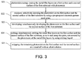
- the present disclosure provides a manufacturing method of a flat panel liquid crystal antenna, the manufacturing method including the following steps:
- the step of simultaneously patterning the metal on the two sides of the first substrate includes the following steps:
- the step of simultaneously patterning the metal on the two sides of the first substrate further includes the following step: stripping: rinsing off the remaining photoresist on the first surface and the second surface of the first substrate to obtain the patterned first metal film layer and the patterned third metal film layer.
- the photoresist coating is to coat the metal film layers on the first surface and the second surface of the first substrate with the photoresist.
- the exposure is to selectively expose the photoresist on the first surface and the second surface of the first substrate simultaneously.
- the exposure is to selectively expose the photoresist on the first surface and the second surface of the first substrate respectively.
- the manufacturing method of the flat panel liquid crystal antenna further includes:
- the present disclosure also provides a flat panel liquid crystal antenna, and the flat panel liquid crystal antenna includes a first substrate and a second substrate which are oppositely arranged and a liquid crystal layer positioned between the first substrate and the second substrate; a patterned first metal film layer is arranged on a first surface, facing the second substrate, of the first substrate; a patterned third metal film layer is arranged on a second surface, facing away from the second substrate, of the first substrate; a patterned second metal film layer is arranged on the side, facing the first substrate, of the second substrate; and the flat panel liquid crystal antenna is manufactured by the manufacturing method described above.
- the patterned first metal film layer includes a first electrode
- the patterned third metal film layer includes an antenna radiation unit
- the patterned second metal film layer includes a second electrode
- the first metal film layer and the third metal film layer are made of the same material.
- the first substrate is a glass substrate
- the material of the first metal film layer and the third metal film layer is copper
- the thickness of the first metal film layer is not less than 2.0 ⁇ m.
- the ratio of the thickness of the first metal film layer to the thickness of the third metal film layer is between 0.8 and 1.2.
- the flat panel liquid crystal antenna can be manufactured on a large scale, the manufacturing efficiency is improved, and the manufacturing cost is reduced.
- a flat panel liquid crystal antenna and a manufacturing method thereof according to the present disclosure will be further described below in conjunction with the drawings and embodiments.
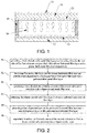
- Fig. 1 shows Embodiment 1 of the present disclosure, which provides a flat panel liquid crystal antenna.
- the flat panel liquid crystal antenna includes a first substrate 11 and a second substrate 12 which are oppositely arranged, and further includes a liquid crystal layer 30 positioned between the first substrate 11 and the second substrate 12.
- the first substrate 11 and the second substrate 12 are made of materials with good stability and insulation effect and extremely low dielectric loss.
- the first substrate 1 1 and the second substrate 12 are rigid substrates, which may be made of a glass material, molten quartz, a ceramic material and a ceramic thermosetting polymer composite.
- a first metal film layer 21 is arranged on a first surface, facing the second substrate 12, of the first substrate 11.
- the first metal film layer 21 is a patterned first metal film layer.
- the patterned first metal film layer 21 includes a first electrode.
- a patterned third metal film layer 23 is arranged on a second surface, facing away from the second substrate 12, of the first substrate 11. Specifically, the third metal film layer 23 is a patterned third metal film layer.
- the third metal film layer 23 includes an antenna radiation unit.
- the antenna radiation unit is used for radiating microwave signals to realize the feed-in and feed-out of microwave signals.
- a patterned second metal film layer 22 is arranged on the side, facing the first substrate 11, of the second substrate 12, and specifically, the second metal film layer 22 is a patterned second metal film layer.
- the second metal film layer 22 includes a second electrode.
- a metal pattern of each patterned metal film layer is obtained by first fabricating a metal film layer on the corresponding substrate and then patterning the metal film layer.
- the fabrication of the metal film layer on the corresponding substrate can be achieved by film coating, that is, coating the substrate with a metal film and forming a planar metal film layer on a surface of the substrate. After film coating, the entire surface of the substrate is coated with the metal film layer which has a structure similar to a plane, so it is referred to herein as a planar metal film layer.
- the patterning process generally includes etching. During etching, the parts, not covered by photoresist, of the metal are etched away by using etching liquid to obtain a metal electrode pattern.
- the patterned first metal film layer and the patterned third metal film layer are obtained by synchronously patterning the first metal film layer and the third metal film layer of the first substrate.
- first metal film layer 21 and the third metal film layer 23 are etched first and then the other is etched according to the conventional process, an etched metal pattern may be destroyed in the subsequent etching process. If the protection for the etched metal pattern is added in the subsequent etching process, an obvious decrease in efficiency may be caused.
- the materials of the first metal film layer 21 and the third metal film layer 23 may be different, but in the present embodiment, the first metal film layer 21 and the third metal film layer 23 are made of the same material.
- the parts, not covered by the photoresist, of the metal film layer need to be etched away in the etching process.
- the etching liquid and the specific parameters of the etching process are generally set according to the metal material and the thickness of the metal film layer.
- the materials of the first metal film layer 21 and the third metal film layer 23 are different, different kinds of etching liquid and different parameters of the etching process are adopted, making simultaneous etching hard to realize.
- the planar first metal film layer 21 and the planar third metal film layer 23 can be simultaneously patterned later. More specifically, it is conducive to simultaneous etching in the later process.
- the thickness of the first metal film layer 21 and the thickness of the third metal film layer 23 are approximately equal. Specifically, the ratio of the thickness of the first metal film layer 21 to the thickness of the third metal film layer 23 is between 0.8 and 1.2. More preferably, the thickness of the first metal film layer 21 and the thickness of the third metal film layer 23 are the same.
- the patterning process generally includes etching. During etching, the parts, not covered by the photoresist, of the metal need to be etched away by using etching liquid to obtain a metal electrode pattern.
- the process of simultaneously patterning the planar first metal film layer 21 and the planar third metal film layer 23 can be made simpler, and the situation that one of the first metal film layer 21 and the third metal film layer 23 is overetched or insufficiently etched is avoided.
- the first substrate 11 is preferably a glass substrate.
- the first metal film layer 21 and the second metal film layer 22 are made of a metal material with high conductivity and magnetic permeability, such as aluminum, copper, silver, gold, cadmium, chromium, molybdenum, niobium, nickel and iron, preferably silver, copper, gold, aluminum and alloys thereof.
- the metal material of the third metal film layer 23 is silver, copper, gold, aluminum, or alloys thereof.
- the material of the first metal film layer 21 and the third metal film layer 23 is copper. It should be understood that the material of the second metal film layer 22 is also preferably copper.
- the skin effect indirectly increases the resistance of a conductor, and its energy heat loss also increases. In high-frequency bands such as microwave, the skin effect is very obvious. Different metal materials have different skin depths.
- Skin effect when there is alternating current or alternating electromagnetic field in the conductor, the current distribution inside the conductor is not uniform, and the current is concentrated on the outer skin part of the conductor; and the closer to the surface of the conductor is, the greater the current density is, and the actual current inside the conductor is very small. As a result, the resistance of the conductor increases and its loss power also increases. This phenomenon is called skin effect.
- the thickness of the metal film layer 21 is of the ⁇ m grade, which can well ensure the performance of the flat panel liquid crystal antenna.
- the thickness of the metal film layer is not less than 2.0 ⁇ m. Therefore, the thickness of the first metal film layer 21 is not less than 2.0 ⁇ m.
- sealant 40 between the first substrate 11 and the second substrate 12.
- the sealant 40 is located at the edges of the first substrate 11 and the second substrate 12 and is used for sealing the liquid crystal layer 30.
- a support material is distributed in the liquid crystal layer 30.
- the flat panel liquid crystal antenna further includes a first alignment layer and a second alignment layer disposed on the two sides of the liquid crystal layer 30 respectively.
- the first alignment layer is prepared on the patterned first metal film layer 21 of the first substrate 11, and the second alignment layer is prepared on the patterned second metal film layer 22 of the second substrate 12.
- the alignment layers are used to define the initial deflection angle of crystal molecules of the liquid crystal layer 30.
- the first substrate 11, the second substrate 12, the liquid crystal layer 30, a first conductive layer, and a second conductive layer constitute a liquid crystal phase shifter.
- the antenna radiation unit is disposed on the side, away from the second substrate 12, of the first substrate 11.
- the antenna radiation unit may be rectangular, circular, or square.
- the antenna radiation unit attaches a patch to the liquid crystal phase shifter through a patch attaching process.
- the antenna radiation unit is obtained by patterning the third metal film layer 23 disposed on the side, away from the second substrate 12, of the first substrate 11.
- a microstrip line is arranged on the second electrode.
- the shape of the microstrip line may be serpentine or spiral, which is not limited, as along as the transmission of the microwave signals can be realized.
- the first electrode is a grounding electrode. By applying a voltage between the microstrip line and the grounding electrode, the dielectric constant of liquid crystal can be changed.
- the liquid crystal molecules are arranged in a preset direction under the action of the first alignment layer and the second alignment layer.
- the electric field drives deflection of the liquid crystal molecules in the liquid crystal layer 30.
- the microwave signals are transmitted between the microstrip line and the grounding electrode. During the transmission of the microwave signals, the phase will be changed due to the deflection of the liquid crystal molecules, thus realizing the phase shift function of the microwave signals.
- the deflection angle of liquid crystals in the liquid crystal layer 30 can be controlled, and further the phase adjusted in the phase shifting process can be controlled.
- the patterning process is made simpler, and the situation that one of the first metal film layer and the third metal film layer is overetched or insufficiently etched is avoided.
- the specific embodiment provides a manufacturing method of a flat panel liquid crystal antenna.
- the manufacturing method is used for manufacturing the flat panel liquid crystal antenna described in the Embodiment 1.
- the manufacturing method includes the following steps:
- the step of simultaneously patterning the metal on the two sides in S2 includes the following steps:
- first metal film layer 21 and the third metal film layer 23 are etched first and then the other is etched according to the conventional process, an etched metal pattern may be destroyed in the subsequent etching process. If the protection for the etched metal pattern is added in the subsequent etching process, an obvious decrease in efficiency may be caused.
- the materials of the first metal film layer 21 and the third metal film layer 23 may be different, but in the present embodiment, the materials of the first metal film layer 21 and the third metal film layer 23 are the same, preferably copper.
- the thickness of the first metal film layer 21 and the thickness of the third metal film layer 23 are approximately equal.
- step S2 of patterning the metal film layer When step S2 of patterning the metal film layer is performed, the parts, not covered by the photoresist, of the metal film layer need to be etched away in the etching process.
- the specific parameters of the etching process are generally set according to the metal material and the thickness of the metal film layer.
- the materials of the first metal film layer 21 and the third metal film layer 23 are different or the materials are the same but the thicknesses of the film layers differ greatly when the first metal film layer 21 and the third metal film layer 23 are etched simultaneously, the result is the etching of one of the first metal film layer 21 and the third metal film layer 23 is finished before the other.
- the first metal film layer 21 and the third metal film layer 23 are made of the same material and have approximately equal thickness, which is advantageous for simultaneous patterning of the planar first metal film layer 21 and the planar third metal film layer 23 later, and more specifically, advantageous for simultaneous etching later.
- the thicknesses are approximately equal, it means that the ratio of the thickness of the first metal film layer 21 to the thickness of the third metal film layer 23 is between 0.8 and 1.2. More preferably, the thickness of the first metal film layer 21 and the thickness of the third metal film layer 23 are the same.
- the patterning process is simpler, and the situation that one of the first metal film layer 21 and the third metal film layer 23 is overetched or insufficiently etched is avoided.
- the entire surface of the metal film layer on the first surface or the metal film layer on the second surface may be coated with the photoresist.
- the photoresist is an exposure medium for etching patterns in subsequent processes. After being coated with the photoresist, one metal film layer is pre-cured. Then the entire surface of the other metal film layer is coated with the photoresist, and then pre-cured. Pre-curing generally involves baking the substrate coated with the photoresist to volatilize a solvent of the photoresist and increase the adhesion between the photoresist and the substrate surface.
- the photoresist on the first surface and the second surface of the first substrate 11 may be exposed simultaneously, or the photoresist on the first surface and the second surface of the first substrate 11 may be exposed in sequence.
- the photoresist is exposed by using the mask plate, so as to form a photoresist non-retained area and a photoresist retained area.
- the photoresist retained area on the first metal film layer 21 corresponds to the area where a pattern of the first electrode is located, and the photoresist non-retained area corresponds to the area other than the pattern.
- ultraviolet light UV
- UV ultraviolet light
- the developed substrate is subjected to high-temperature hard-baking to make the photoresist firmer.
- the parts, not covered by the photoresist, of the metal film layer are etched away, and the parts, covered by the photoresist, of the metal film layer are protected by the photoresist to form a metal pattern structure.
- a pattern of the first electrode is formed on the first metal film layer 21, and a pattern of the antenna radiation unit is formed on the third metal film layer 23.
- step S2 of simultaneously patterning the metal on the two sides further includes the following step: S25: stripping: as the etched metal film layer is still covered with the photoresist on the metal pattern, by stripping, the remaining photoresist on the first surface and the second surface are rinsed off with an alkali solution, so as to obtain the patterned first metal film layer 21 and the patterned third metal film layer 23.
- the first surface and the second surface of the first substrate 11 may be stripped one by one. Alternatively, the first surface and the second surface of the first substrate 11 may be simultaneously stripped.
- the specific step of patterning the second metal film layer 22 can be performed with reference to the above process step of patterning the first metal film layer 21.
- the manufacturing method of the flat panel liquid crystal antenna also includes the following steps:
- the alignment layers may be made by PI friction process in the prior art so as to form orientation grooves on the surfaces, which will not be detailed here.
- the first substrate 11 and the second substrate 12 may be first aligned and assembled to form the liquid crystal cell, which is then filled with the liquid crystal layer 30. It is known that before the first substrate 11 and the second substrate 12 are aligned and assembled, sealant 40 is also prepared on one of the substrates, and the sealant 40 defines an accommodation space between the first substrate 11 and the second substrate 12 for accommodating liquid crystals. After the liquid crystal cell is filled with the liquid crystal layer 30, the liquid crystal cell is sealed and the sealant 40 is cured.
- the order of oppositely bonding to form the liquid crystal cell and preparing the liquid crystal layer 30 is not limited to the above, but may also be: after coating one of the substrates with the sealant 40, dripping liquid crystals onto the substrate to form the liquid crystal layer 30, oppositely bonding the first substrate 11 and the second substrate 12 to form the liquid crystal cell, and then curing the sealant 40.
- the present disclosure has the following beneficial effects: Through simultaneous patterning of the metal on the two sides of the first substrate, patterns on two sides can be produced at one time, most low-efficiency yellow-light procedures are omitted, and time for busy waiting, model switching, etc. is saved.
- the flat panel liquid crystal antenna can be manufactured on a large scale, the manufacturing efficiency is improved, and the manufacturing cost is reduced.
- the present disclosure avoids the situation occurring in the traditional process that as the first metal film layer and the third metal film layer are etched one by one, an etched metal pattern may be destroyed in the subsequent etching process, and in order to avoid damaging the etched metal pattern, a significant decrease in efficiency may be caused.
Landscapes
- Physics & Mathematics (AREA)
- Engineering & Computer Science (AREA)
- Manufacturing & Machinery (AREA)
- Nonlinear Science (AREA)
- Mathematical Physics (AREA)
- Crystallography & Structural Chemistry (AREA)
- Chemical & Material Sciences (AREA)
- General Physics & Mathematics (AREA)
- Optics & Photonics (AREA)
- Microelectronics & Electronic Packaging (AREA)
- Liquid Crystal (AREA)
- Details Of Aerials (AREA)
- Variable-Direction Aerials And Aerial Arrays (AREA)
Applications Claiming Priority (2)
| Application Number | Priority Date | Filing Date | Title |
|---|---|---|---|
| CN201910185143.7A CN109830806A (zh) | 2019-03-12 | 2019-03-12 | 一种平板液晶天线及其制作方法 |
| PCT/CN2019/078172 WO2020181556A1 (fr) | 2019-03-12 | 2019-03-14 | Antenne à cristaux liquides plate et son procédé de fabrication |
Publications (2)
| Publication Number | Publication Date |
|---|---|
| EP3736618A1 true EP3736618A1 (fr) | 2020-11-11 |
| EP3736618A4 EP3736618A4 (fr) | 2021-03-24 |
Family
ID=66869147
Family Applications (1)
| Application Number | Title | Priority Date | Filing Date |
|---|---|---|---|
| EP19863988.2A Pending EP3736618A4 (fr) | 2019-03-12 | 2019-03-14 | Antenne à cristaux liquides plate et son procédé de fabrication |
Country Status (7)
| Country | Link |
|---|---|
| US (1) | US11557837B2 (fr) |
| EP (1) | EP3736618A4 (fr) |
| JP (1) | JP7042342B2 (fr) |
| KR (1) | KR102326747B1 (fr) |
| CN (1) | CN109830806A (fr) |
| TW (1) | TWI742561B (fr) |
| WO (1) | WO2020181556A1 (fr) |
Families Citing this family (8)
| Publication number | Priority date | Publication date | Assignee | Title |
|---|---|---|---|---|
| CN112394609A (zh) * | 2019-08-16 | 2021-02-23 | 合肥晶合集成电路股份有限公司 | 掩模板及曝光方法 |
| CN111525264B (zh) * | 2020-05-21 | 2022-01-18 | 信利(仁寿)高端显示科技有限公司 | 一种液晶天线 |
| CN114447586B (zh) * | 2020-10-30 | 2025-06-13 | 京东方科技集团股份有限公司 | 可重构天线及其制备方法 |
| US11990680B2 (en) * | 2021-03-18 | 2024-05-21 | Seoul National University R&Db Foundation | Array antenna system capable of beam steering and impedance control using active radiation layer |
| CN114284714B (zh) * | 2021-12-31 | 2023-12-15 | 成都天马微电子有限公司 | 液晶天线及其制备方法 |
| CN116830383A (zh) | 2022-01-27 | 2023-09-29 | 京东方科技集团股份有限公司 | 移相器及天线 |
| CN116514406A (zh) * | 2023-04-26 | 2023-08-01 | 深圳市志凌伟业技术股份有限公司 | 一种玻璃基透明导电片的制备方法 |
| KR102886770B1 (ko) * | 2023-09-27 | 2025-12-26 | 대한민국(방위사업청장) | 액정 기반 배열 안테나의 액정 물성 추출 방법 |
Family Cites Families (20)
| Publication number | Priority date | Publication date | Assignee | Title |
|---|---|---|---|---|
| JPH02162804A (ja) * | 1988-12-16 | 1990-06-22 | Nissan Motor Co Ltd | 平板型アンテナ |
| CN102541368A (zh) * | 2011-03-14 | 2012-07-04 | 烟台正海电子网板股份有限公司 | 一种电容式触控面板及其制造方法 |
| CN102339402B (zh) * | 2011-09-15 | 2014-02-05 | 哈尔滨大东方新材料科技股份有限公司 | 利用热、冷烫印技术制作射频标签的方法 |
| EP2575211B1 (fr) * | 2011-09-27 | 2014-11-05 | Technische Universität Darmstadt | Antenne de réseau phasée planaire orientable électroniquement |
| CN102751584B (zh) * | 2012-06-12 | 2014-08-06 | 西安电子科技大学 | 基于两层基板的小型化人工电磁材料及制备方法 |
| CN102931199A (zh) * | 2012-11-02 | 2013-02-13 | 京东方科技集团股份有限公司 | 一种显示面板及制作方法、显示装置 |
| EP2784181B1 (fr) | 2013-03-27 | 2015-12-09 | ATOTECH Deutschland GmbH | Solution de dépôt de cuivre chimique |
| JP6070675B2 (ja) | 2014-10-27 | 2017-02-01 | 大日本印刷株式会社 | 透明導電基材の製造方法およびタッチパネルセンサ |
| JP2017106984A (ja) * | 2015-12-07 | 2017-06-15 | 大日本印刷株式会社 | 調光パネル及び調光パネルを備えた窓 |
| JP6589058B2 (ja) * | 2016-05-30 | 2019-10-09 | シャープ株式会社 | 走査アンテナ |
| US10720708B2 (en) * | 2016-07-25 | 2020-07-21 | Innolux Corporation | Antenna device |
| CN108321503B (zh) * | 2017-01-16 | 2020-05-15 | 群创光电股份有限公司 | 液晶天线装置 |
| CN108321504B (zh) * | 2017-01-16 | 2020-11-10 | 群创光电股份有限公司 | 可调制微波装置 |
| CN206602182U (zh) * | 2017-04-06 | 2017-10-31 | 京东方科技集团股份有限公司 | 一种天线结构及通讯设备 |
| CN106932933B (zh) | 2017-05-09 | 2019-08-27 | 京东方科技集团股份有限公司 | 一种液晶天线及其制作方法 |
| DE102017212887A1 (de) * | 2017-07-26 | 2019-01-31 | Gebr. Schmid Gmbh | Verfahren, Vorrichtung und Anlage zur Leiterplattenherstellung |
| CN208589535U (zh) * | 2018-04-02 | 2019-03-08 | 武汉光谷创元电子有限公司 | Lcp单层或多层板天线 |
| CN108490706B (zh) | 2018-04-13 | 2024-04-02 | 京东方科技集团股份有限公司 | 液晶移相器及其制造方法、液晶天线及电子装置 |
| CN108615966B (zh) * | 2018-05-28 | 2020-06-30 | 京东方科技集团股份有限公司 | 一种天线及其制作方法 |
| CN108963402B (zh) * | 2018-08-16 | 2023-09-26 | 北京华镁钛科技有限公司 | 一种用于制作射频微波器件及天线的传输结构及制作方法 |
-
2019
- 2019-03-12 CN CN201910185143.7A patent/CN109830806A/zh active Pending
- 2019-03-14 JP JP2020531664A patent/JP7042342B2/ja active Active
- 2019-03-14 KR KR1020207016582A patent/KR102326747B1/ko active Active
- 2019-03-14 US US16/770,078 patent/US11557837B2/en active Active
- 2019-03-14 WO PCT/CN2019/078172 patent/WO2020181556A1/fr not_active Ceased
- 2019-03-14 EP EP19863988.2A patent/EP3736618A4/fr active Pending
-
2020
- 2020-03-12 TW TW109108211A patent/TWI742561B/zh active
Also Published As
| Publication number | Publication date |
|---|---|
| WO2020181556A1 (fr) | 2020-09-17 |
| JP7042342B2 (ja) | 2022-03-25 |
| TWI742561B (zh) | 2021-10-11 |
| US11557837B2 (en) | 2023-01-17 |
| KR102326747B1 (ko) | 2021-11-15 |
| CN109830806A (zh) | 2019-05-31 |
| EP3736618A4 (fr) | 2021-03-24 |
| US20210210852A1 (en) | 2021-07-08 |
| TW202103375A (zh) | 2021-01-16 |
| KR20200110307A (ko) | 2020-09-23 |
| JP2021517746A (ja) | 2021-07-26 |
Similar Documents
| Publication | Publication Date | Title |
|---|---|---|
| US11557837B2 (en) | Flat panel liquid crystal antenna and manufacturing method thereof | |
| EP3745527B1 (fr) | Déphaseur à cristaux liquides, antenne à cristaux liquides, et procédé de fabrication de déphaseur à cristaux liquides | |
| EP3736626B1 (fr) | Antenne à cristaux liquides et son procédé de fabrication | |
| CN210720940U (zh) | 一种液晶盒、液晶天线单元和液晶相控阵天线 | |
| EP3736625B1 (fr) | Déphaseur à cristaux liquides et son procédé de fabrication | |
| CN209544568U (zh) | 一种液晶移相器和液晶天线 | |
| US11646488B2 (en) | Liquid crystal phase shifter having a delay line with line spacing and/or line width that provides a specified cell thickness and an antenna formed therefrom | |
| CN113950772B (zh) | 移相器及其制备方法、天线 | |
| US20210215956A1 (en) | Liquid crystal antenna substrate and manufacturing method thereof, and liquid crystal antenna and manufacturing method thereof | |
| CN209786195U (zh) | 一种液晶天线 | |
| CN209544616U (zh) | 一种平板液晶天线 | |
| CN215578989U (zh) | 移相器和天线 | |
| Martynyuk et al. | 2-bit $ X $-band reflective waveguide phase shifter with BCB-based bias circuits | |
| CN115051156B (zh) | 天线及其制作方法 | |
| CN115882222A (zh) | 一种基于微金属线结构的高透光率宽带透射阵天线 | |
| CN113871864A (zh) | 液晶天线及其制作方法 | |
| CN120073255A (zh) | 一种移相器、其制作方法及电子设备 | |
| CN113917742A (zh) | 一种叠层液晶天线及其制造方法 |
Legal Events
| Date | Code | Title | Description |
|---|---|---|---|
| STAA | Information on the status of an ep patent application or granted ep patent |
Free format text: STATUS: UNKNOWN |
|
| STAA | Information on the status of an ep patent application or granted ep patent |
Free format text: STATUS: THE INTERNATIONAL PUBLICATION HAS BEEN MADE |
|
| PUAI | Public reference made under article 153(3) epc to a published international application that has entered the european phase |
Free format text: ORIGINAL CODE: 0009012 |
|
| STAA | Information on the status of an ep patent application or granted ep patent |
Free format text: STATUS: REQUEST FOR EXAMINATION WAS MADE |
|
| 17P | Request for examination filed |
Effective date: 20200331 |
|
| AK | Designated contracting states |
Kind code of ref document: A1 Designated state(s): AL AT BE BG CH CY CZ DE DK EE ES FI FR GB GR HR HU IE IS IT LI LT LU LV MC MK MT NL NO PL PT RO RS SE SI SK SM TR |
|
| AX | Request for extension of the european patent |
Extension state: BA ME |
|
| A4 | Supplementary search report drawn up and despatched |
Effective date: 20210222 |
|
| RIC1 | Information provided on ipc code assigned before grant |
Ipc: H01P 1/18 20060101ALI20210216BHEP Ipc: G02F 1/13 20060101AFI20210216BHEP Ipc: H01Q 3/36 20060101ALI20210216BHEP Ipc: H01P 11/00 20060101ALI20210216BHEP Ipc: H05K 3/06 20060101ALI20210216BHEP |
|
| DAV | Request for validation of the european patent (deleted) | ||
| DAX | Request for extension of the european patent (deleted) | ||
| STAA | Information on the status of an ep patent application or granted ep patent |
Free format text: STATUS: EXAMINATION IS IN PROGRESS |
|
| 17Q | First examination report despatched |
Effective date: 20230217 |