EP3732671B1 - Écran d'affichage à diodes électroluminescentes - Google Patents
Écran d'affichage à diodes électroluminescentes Download PDFInfo
- Publication number
- EP3732671B1 EP3732671B1 EP18811319.5A EP18811319A EP3732671B1 EP 3732671 B1 EP3732671 B1 EP 3732671B1 EP 18811319 A EP18811319 A EP 18811319A EP 3732671 B1 EP3732671 B1 EP 3732671B1
- Authority
- EP
- European Patent Office
- Prior art keywords
- signal
- transistor
- display screen
- circuit
- display
- Prior art date
- Legal status (The legal status is an assumption and is not a legal conclusion. Google has not performed a legal analysis and makes no representation as to the accuracy of the status listed.)
- Active
Links
Images
Classifications
-
- G—PHYSICS
- G09—EDUCATION; CRYPTOGRAPHY; DISPLAY; ADVERTISING; SEALS
- G09G—ARRANGEMENTS OR CIRCUITS FOR CONTROL OF INDICATING DEVICES USING STATIC MEANS TO PRESENT VARIABLE INFORMATION
- G09G3/00—Control arrangements or circuits, of interest only in connection with visual indicators other than cathode-ray tubes
- G09G3/20—Control arrangements or circuits, of interest only in connection with visual indicators other than cathode-ray tubes for presentation of an assembly of a number of characters, e.g. a page, by composing the assembly by combination of individual elements arranged in a matrix no fixed position being assigned to or needed to be assigned to the individual characters or partial characters
- G09G3/22—Control arrangements or circuits, of interest only in connection with visual indicators other than cathode-ray tubes for presentation of an assembly of a number of characters, e.g. a page, by composing the assembly by combination of individual elements arranged in a matrix no fixed position being assigned to or needed to be assigned to the individual characters or partial characters using controlled light sources
- G09G3/30—Control arrangements or circuits, of interest only in connection with visual indicators other than cathode-ray tubes for presentation of an assembly of a number of characters, e.g. a page, by composing the assembly by combination of individual elements arranged in a matrix no fixed position being assigned to or needed to be assigned to the individual characters or partial characters using controlled light sources using electroluminescent panels
- G09G3/32—Control arrangements or circuits, of interest only in connection with visual indicators other than cathode-ray tubes for presentation of an assembly of a number of characters, e.g. a page, by composing the assembly by combination of individual elements arranged in a matrix no fixed position being assigned to or needed to be assigned to the individual characters or partial characters using controlled light sources using electroluminescent panels semiconductive, e.g. using light-emitting diodes [LED]
-
- G—PHYSICS
- G09—EDUCATION; CRYPTOGRAPHY; DISPLAY; ADVERTISING; SEALS
- G09G—ARRANGEMENTS OR CIRCUITS FOR CONTROL OF INDICATING DEVICES USING STATIC MEANS TO PRESENT VARIABLE INFORMATION
- G09G3/00—Control arrangements or circuits, of interest only in connection with visual indicators other than cathode-ray tubes
- G09G3/20—Control arrangements or circuits, of interest only in connection with visual indicators other than cathode-ray tubes for presentation of an assembly of a number of characters, e.g. a page, by composing the assembly by combination of individual elements arranged in a matrix no fixed position being assigned to or needed to be assigned to the individual characters or partial characters
- G09G3/2007—Display of intermediate tones
- G09G3/2014—Display of intermediate tones by modulation of the duration of a single pulse during which the logic level remains constant
-
- G—PHYSICS
- G09—EDUCATION; CRYPTOGRAPHY; DISPLAY; ADVERTISING; SEALS
- G09G—ARRANGEMENTS OR CIRCUITS FOR CONTROL OF INDICATING DEVICES USING STATIC MEANS TO PRESENT VARIABLE INFORMATION
- G09G3/00—Control arrangements or circuits, of interest only in connection with visual indicators other than cathode-ray tubes
- G09G3/20—Control arrangements or circuits, of interest only in connection with visual indicators other than cathode-ray tubes for presentation of an assembly of a number of characters, e.g. a page, by composing the assembly by combination of individual elements arranged in a matrix no fixed position being assigned to or needed to be assigned to the individual characters or partial characters
- G09G3/22—Control arrangements or circuits, of interest only in connection with visual indicators other than cathode-ray tubes for presentation of an assembly of a number of characters, e.g. a page, by composing the assembly by combination of individual elements arranged in a matrix no fixed position being assigned to or needed to be assigned to the individual characters or partial characters using controlled light sources
- G09G3/30—Control arrangements or circuits, of interest only in connection with visual indicators other than cathode-ray tubes for presentation of an assembly of a number of characters, e.g. a page, by composing the assembly by combination of individual elements arranged in a matrix no fixed position being assigned to or needed to be assigned to the individual characters or partial characters using controlled light sources using electroluminescent panels
- G09G3/32—Control arrangements or circuits, of interest only in connection with visual indicators other than cathode-ray tubes for presentation of an assembly of a number of characters, e.g. a page, by composing the assembly by combination of individual elements arranged in a matrix no fixed position being assigned to or needed to be assigned to the individual characters or partial characters using controlled light sources using electroluminescent panels semiconductive, e.g. using light-emitting diodes [LED]
- G09G3/3208—Control arrangements or circuits, of interest only in connection with visual indicators other than cathode-ray tubes for presentation of an assembly of a number of characters, e.g. a page, by composing the assembly by combination of individual elements arranged in a matrix no fixed position being assigned to or needed to be assigned to the individual characters or partial characters using controlled light sources using electroluminescent panels semiconductive, e.g. using light-emitting diodes [LED] organic, e.g. using organic light-emitting diodes [OLED]
- G09G3/3225—Control arrangements or circuits, of interest only in connection with visual indicators other than cathode-ray tubes for presentation of an assembly of a number of characters, e.g. a page, by composing the assembly by combination of individual elements arranged in a matrix no fixed position being assigned to or needed to be assigned to the individual characters or partial characters using controlled light sources using electroluminescent panels semiconductive, e.g. using light-emitting diodes [LED] organic, e.g. using organic light-emitting diodes [OLED] using an active matrix
- G09G3/3233—Control arrangements or circuits, of interest only in connection with visual indicators other than cathode-ray tubes for presentation of an assembly of a number of characters, e.g. a page, by composing the assembly by combination of individual elements arranged in a matrix no fixed position being assigned to or needed to be assigned to the individual characters or partial characters using controlled light sources using electroluminescent panels semiconductive, e.g. using light-emitting diodes [LED] organic, e.g. using organic light-emitting diodes [OLED] using an active matrix with pixel circuitry controlling the current through the light-emitting element
-
- G—PHYSICS
- G09—EDUCATION; CRYPTOGRAPHY; DISPLAY; ADVERTISING; SEALS
- G09G—ARRANGEMENTS OR CIRCUITS FOR CONTROL OF INDICATING DEVICES USING STATIC MEANS TO PRESENT VARIABLE INFORMATION
- G09G3/00—Control arrangements or circuits, of interest only in connection with visual indicators other than cathode-ray tubes
- G09G3/20—Control arrangements or circuits, of interest only in connection with visual indicators other than cathode-ray tubes for presentation of an assembly of a number of characters, e.g. a page, by composing the assembly by combination of individual elements arranged in a matrix no fixed position being assigned to or needed to be assigned to the individual characters or partial characters
- G09G3/22—Control arrangements or circuits, of interest only in connection with visual indicators other than cathode-ray tubes for presentation of an assembly of a number of characters, e.g. a page, by composing the assembly by combination of individual elements arranged in a matrix no fixed position being assigned to or needed to be assigned to the individual characters or partial characters using controlled light sources
- G09G3/30—Control arrangements or circuits, of interest only in connection with visual indicators other than cathode-ray tubes for presentation of an assembly of a number of characters, e.g. a page, by composing the assembly by combination of individual elements arranged in a matrix no fixed position being assigned to or needed to be assigned to the individual characters or partial characters using controlled light sources using electroluminescent panels
- G09G3/32—Control arrangements or circuits, of interest only in connection with visual indicators other than cathode-ray tubes for presentation of an assembly of a number of characters, e.g. a page, by composing the assembly by combination of individual elements arranged in a matrix no fixed position being assigned to or needed to be assigned to the individual characters or partial characters using controlled light sources using electroluminescent panels semiconductive, e.g. using light-emitting diodes [LED]
- G09G3/3208—Control arrangements or circuits, of interest only in connection with visual indicators other than cathode-ray tubes for presentation of an assembly of a number of characters, e.g. a page, by composing the assembly by combination of individual elements arranged in a matrix no fixed position being assigned to or needed to be assigned to the individual characters or partial characters using controlled light sources using electroluminescent panels semiconductive, e.g. using light-emitting diodes [LED] organic, e.g. using organic light-emitting diodes [OLED]
- G09G3/3275—Details of drivers for data electrodes
- G09G3/3291—Details of drivers for data electrodes in which the data driver supplies a variable data voltage for setting the current through, or the voltage across, the light-emitting elements
-
- G—PHYSICS
- G09—EDUCATION; CRYPTOGRAPHY; DISPLAY; ADVERTISING; SEALS
- G09G—ARRANGEMENTS OR CIRCUITS FOR CONTROL OF INDICATING DEVICES USING STATIC MEANS TO PRESENT VARIABLE INFORMATION
- G09G2300/00—Aspects of the constitution of display devices
- G09G2300/08—Active matrix structure, i.e. with use of active elements, inclusive of non-linear two terminal elements, in the pixels together with light emitting or modulating elements
- G09G2300/0809—Several active elements per pixel in active matrix panels
- G09G2300/0842—Several active elements per pixel in active matrix panels forming a memory circuit, e.g. a dynamic memory with one capacitor
- G09G2300/0861—Several active elements per pixel in active matrix panels forming a memory circuit, e.g. a dynamic memory with one capacitor with additional control of the display period without amending the charge stored in a pixel memory, e.g. by means of additional select electrodes
-
- G—PHYSICS
- G09—EDUCATION; CRYPTOGRAPHY; DISPLAY; ADVERTISING; SEALS
- G09G—ARRANGEMENTS OR CIRCUITS FOR CONTROL OF INDICATING DEVICES USING STATIC MEANS TO PRESENT VARIABLE INFORMATION
- G09G2320/00—Control of display operating conditions
- G09G2320/06—Adjustment of display parameters
- G09G2320/0626—Adjustment of display parameters for control of overall brightness
- G09G2320/064—Adjustment of display parameters for control of overall brightness by time modulation of the brightness of the illumination source
-
- G—PHYSICS
- G09—EDUCATION; CRYPTOGRAPHY; DISPLAY; ADVERTISING; SEALS
- G09G—ARRANGEMENTS OR CIRCUITS FOR CONTROL OF INDICATING DEVICES USING STATIC MEANS TO PRESENT VARIABLE INFORMATION
- G09G2330/00—Aspects of power supply; Aspects of display protection and defect management
- G09G2330/02—Details of power systems and of start or stop of display operation
- G09G2330/025—Reduction of instantaneous peaks of current
Definitions
- the present application relates to a display screen whose display pixels comprise light-emitting diodes, whatever their type of technology (2D, 3D light-emitting diode, organic light-emitting diode, etc.)
- the display pixels of an LED display panel may include, for each display pixel, an LED driver circuit or LEDs of the display pixel.
- PWM pulse width modulation
- An object of an embodiment is to provide a light-emitting diode display screen overcoming all or part of the drawbacks of existing light-emitting diode display screens.
- Another object of an embodiment is for the display screen driver circuitry to implement pulse width modulation.
- Another object of an embodiment is that the display pixels have dimensions less than 200 ⁇ m.
- a “binary signal” is a signal which alternates between a first constant state, for example a low state, denoted “0”, and a second constant state, for example a high state, denoted “1”.
- the high and low states of different binary signals of the same electronic circuit can be different.
- binary signals may correspond to voltages or currents which may not be perfectly constant in the high or low state.
- the term “power terminals” of an insulated-gate field-effect transistor, or MOS transistor refers to the source and the drain of the MOS transistor.
- a first binary signal is said to be "synchronous" with a second binary signal when the rising and/or falling edges of the first signal occur at the same time as the rising and/or falling edges of the second signal or occur at regular intervals relative to the rising and/or falling edges of the second signal.
- synchronous binary signals derive from a common clock.
- first and second binary signals are said to be “asynchronous” or “non-synchronous” when the rising and/or falling edges of the first signal occur neither at the same time as the rising and/or falling edges of the second signal nor at intervals regular with respect to the rising and/or falling edges of the second signal.
- asynchronous binary signals do not derive from the same clock.
- a pixel of an image corresponds to the unitary element of the image displayed by a display screen.
- the display screen is a color image display screen, it generally comprises for the display of each pixel of the image at least three emission and/or light intensity regulation components , also called display sub-pixels, which each emit light radiation substantially in a single color (for example, red, green, and blue). The superposition of the radiation emitted by these three display sub-pixels provides the observer with the colored sensation corresponding to the pixel of the displayed image.
- the display screen is a monochrome image display screen
- the display screen generally comprises a single light source for displaying each pixel of the image.
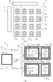
- the figure 1 partially and schematically represents an embodiment of a display screen 10.
- the display screen 10 comprises display circuits 12 i,j for example arranged in M rows and in N columns, M being an integer varying from 1 to 16000 and N being an integer varying from 1 to 8000, i being an integer varying from 1 to M and j being an integer varying from 1 to N.
- M and N are equal to 4.
- Each display circuit 12 i,j comprises a control circuit 14 i,j and a display sub-pixel 16 i,j .
- Each display sub-pixel 16 i,j comprises at least one light-emitting diode, not shown.
- control circuits 14 i,j of the display circuits 12 i,j of the row are connected to a row electrode 18 i .
- control circuits 14 i,j of the display circuits 12 i,j of the column are connected to a column electrode 20 j .
- the display screen 10 comprises a selection circuit 22 connected to the row electrodes 18 i and adapted to provide a selection signal VSelect i on each row electrode 18 i .
- the display screen 10 comprises a control circuit 24 connected to the column electrodes 20 j and adapted to supply a data signal Data j,j on each column electrode 20 j .
- the figure 2 represents a more detailed embodiment of two display circuits 12 i,j and 12 i+1,j of the display screen 10.
- the display screen 10 comprises oscillating circuits OSC for supplying oscillating and periodic signals ST connected to the display circuits 12 i,j and 12 i+1,j .
- Each display sub-pixel 16 i,j comprises a light-emitting diode LED i,j connected in series to a controllable current source CS i,j .
- Each control circuit 14 i,j comprises a memory circuit 26 i,j connected to the row electrode 18 i and to the column electrode 20 j .
- the memory circuit 26 i,j is controlled by the signal VSelect i supplied by the row electrode 18 i and is adapted to store the signal Data i,j supplied by the column electrode 20 j .
- the memory circuit 26 i,j comprises a switch SW i,j controlled by the signal VSelect i and a capacitor C1 i,j .
- the first terminal of switch SW i,j is connected to column electrode 20 j and the second terminal of switch SW i,j is connected to the first electrode of capacitor C1 i,j , the second electrode of capacitor C1 i,j being connected to a source GND of a low reference potential, eg ground.
- Each control circuit 14 i,j further comprises a comparison circuit COMP i,j connected to a first input (+) to the oscillating circuit OSC and connected to a second input (-) to the first electrode of the capacitor C1 i ,j .
- the comparison circuit COMP i,j supplies a signal PWM i,j for controlling the current source CS i,j .
- the Vselect i signal is a binary signal.
- the switch SW i,j When the signal Vselect i is in a first state, for example the low state, the switch SW i,j is open and when the signal Vselect i is in a second state, for example the high state, the switch SW i,j is closed.
- the Data i,j signals are analog signals representative of the desired light intensities to be emitted by the light-emitting diodes LED i,j .
- switch SW i,j is closed, the voltage across capacitor C1 i,j becomes substantially equal to signal Data i,j .
- the PWM signal i,j is a binary signal which depends on the comparison between the signal ST and the voltage across the terminals of the capacitor C1 i,j , that is to say the signal Data i,j .
- the PWM i,j signal is in a first state, for example the high state, when the ST signal is greater than the Data i,j signal and the PWM i,j signal is in a second state, for example the low state, when the signal ST is lower than the signal Data i,j .
- the signal ST is a periodic signal which, over each period, continuously increases or decreases continuously over substantially the entire period.
- the signal ST is a sawtooth signal which, over each period, increases or decreases at a substantially constant slope.
- the PWM signal i,j obtained is then a cyclic signal modulated in pulse width, the duration of the PWM signal i,j in the high state over one cycle being proportional to the signal Data i,j .
- the current source CS i,j is controlled by the signal PMM i,j .
- the current source CS i,j is activated, that is to say that it supplies the light-emitting diode LED i,j with current, when the PWM signal i,j is in the first state , for example the high state, and the current source CS i,j is deactivated, that is to say that the light-emitting diode LED i,j is not traversed by a current, when the PWM signal i,j is in the second state, for example the low state.
- the current supplied by the current source CS i,j is preferably substantially constant and equal to the current for which the efficiency of the light-emitting diode LED i,j is maximum.
- the light-emitting diode LED i,j is therefore either supplied at constant current or switched off. Control of the light-emitting diode LED i,j by pulse width modulation is thus obtained.
- the oscillating circuit OSC is by way of example connected to two display circuits 12 i,j and 12 i+1,j , which is not part of the invention and is present by way of example only.
- the display screen 10 comprises several oscillating circuits OSC, each oscillating circuit OSC being connected to a display circuit 12 i,j .
- the display screen 10 comprises an oscillating circuit OSC for each display circuit 12 i,j .
- the rows of display sub-pixels are activated successively.
- the signals Vselect 1 to VSelect M are then successively set to the high state for a duration ⁇ T, the signals Vselect 1 to VSelect i-1 and Vselect i+1 to VSelect M being in the low state when the signal Vselect i is in the high state.
- F the refresh rate of the display screen.
- the frequency F is equal to 1/ ⁇ T.
- the frequency F varies from 25 Hz to 120 Hz.
- the frequency F' of the signal ST is greater than 2 times the frequency F, preferably greater than 10 times the frequency F, more preferably greater than 100 times the frequency F.
- the frequency F′ is greater than 1 kHz, preferably greater than 10 kHz, even more preferably greater than 100 kHz.
- the frequency F' of the signal ST is preferably less than 1 MHz.
- the structure of the oscillating circuit OSC can then be simple. Furthermore, when the oscillating circuit OSC implements switches, the losses due to the switching of the switches are low.
- the signal ST is not synchronous with the signals VSelect i and Data i,j . This means that the start of each period of the signal ST is not synchronous with the instants at which the signals Vselect i change state.
- the signals ST supplied by the oscillating circuits OSC are not mutually synchronous.
- the design of the display screen 10 is then simplified since there is no need to keep the signals ST synchronous with each other and with the signals VSelect i and Data i,j .
- the current surges during the operation of the display screen 10 are advantageously spread over time.
- the number of conductive tracks connecting the oscillating circuit OSC and the associated control circuit 14 i,j is reduced.
- the distance traveled by the signal ST between each oscillating circuit OSC and the display circuit 12 i,j to which the oscillating circuit OSC is connected can be reduced compared to the case where a clock signal must be supplied to each circuit of display 12 i,j .
- the display sub-pixels 16 i,j can be formed on a first electronic circuit and the control circuits 14 i,j and the oscillating circuits OSC can be formed on a second electronic circuit, the first and second electronic circuits being fixed to one another.
- the control circuits 14 i,j and the oscillating circuits OSC can be formed using CMOS technology.
- the control circuits 14 i,j and the oscillating circuits OSC can be formed with thin film transistors.
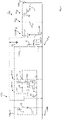
- the picture 3 represents an embodiment of an oscillating circuit OSC and of a display circuit 12 i,j of the display screen 10 of the figure 1 .
- the switch SW i,j of the memory circuit 26 i,j of the control circuit 14 i,j corresponds to an MOS transistor T1, for example with N channel, whose gate receives the signal Vselect i , whose first bound power receives the signal Data i,j and whose second power terminal is connected to a first electrode of the capacitor C1 i,j .
- the comparison circuit COMP i,j comprises a MOS transistor T2, for example with a P channel, whose gate is connected to the first electrode of the capacitor C1 i,j , whose first power terminal receives the signal ST and whose second power terminal is connected to the source GND of the low reference potential via a resistor R1.
- the PWM signal i,j supplied by the comparison circuit COMP i,j corresponds to the voltage at the second power terminal of the transistor T2.
- the controllable current source CS i,j comprises two series MOS transistors T3 and T4, for example N-channel transistors.
- the gate of transistor T3 is connected to the second power terminal of transistor T2.
- the first power terminal of transistor T3 is connected to the cathode of light-emitting diode LED i,j and the second power terminal of transistor T3 is connected to the first power terminal of transistor T4.
- the gate of transistor T3 receives signal PMM i,j .
- the anode of the light-emitting diode LED i,j is connected to a source VREF1 of a first high reference potential, for example the supply voltage of the display screen 10.
- the gate of the transistor T4 is connected to a source VREF2 of a second high reference potential.
- the second power terminal of transistor T4 is connected to the source GND of the low reference potential.
- the controllable current source created by transistors T4 and T3 is designed to draw current from the cathode of the LED to ground GND, the anode of the LED being connected to the high supply potential VREF1 .
- This structure is particularly suitable for an LED technology whose equivalent electrical representation of the pixels would be a structure with a common anode.
- Those skilled in the art can easily modify the structure of the current source as well as its control to adapt it to a technology of LED/OLED whose electrical representation would be a common cathode type structure or more generally a structure where the cathode of the LED would be connected to ground.
- the current source should then be placed between the anode of the LED and a high potential (VREF1 for example)
- the oscillating circuit OSC comprises an MOS transistor T5, for example with P channel, whose first power terminal is connected to the source VREF1 of the first high reference potential and whose second power terminal is connected to a node Q supplying the signal ST.
- Oscillating circuit OSC further comprises a capacitor C2 whose first electrode is connected to node Q and whose second electrode is connected to source GND of the low reference potential.
- Oscillating circuit OSC further comprises an N-channel MOS transistor T6, for example, whose first power terminal is connected to node Q and whose second power terminal is connected to source GND of the low reference potential.
- the oscillating circuit OSC further comprises a first inverter INV1 whose input is connected to the node Q and whose output is connected to a node R.
- the first inverter INV1 may include a MOS transistor T7, for example with a P channel, in series with an N-channel MOS transistor T8, for example.
- the first power terminal of transistor T7 is connected to source VREF1 of the first high reference potential and the second power terminal of transistor T7 is connected to node R.
- first power terminal of transistor T8 is connected to node R and the second power terminal of transistor T8 is connected to source GND of the low reference potential.
- the gates of transistors T7 and T8 are connected to node Q.
- Oscillating circuit OSC further comprises a second inverter INV2 whose input is connected to node R and whose output is connected to a node S.
- Second inverter INV2 may comprise a P-channel MOS transistor T9, for example, in series with an N-channel MOS transistor T10, for example.
- the first power terminal of the transistor T9 is connected to the source VREF1 of the first high reference potential and the second power of transistor T9 is connected at node S.
- the first power terminal of transistor T10 is connected to node S and the second power terminal of transistor T10 is connected to source GND of the low reference potential.
- the gates of transistors T9 and T10 are connected to node S.
- Oscillating circuit OSC further comprises an N-channel MOS transistor T11, for example, whose first power terminal is connected to node R and whose second power is connected to the source GND of the low reference potential and an MOS transistor T12, for example N-channel, whose first power terminal is connected to the node R and whose second power terminal is connected to the source GND of the potential low reference.
- the gates of transistors T5, T6, T11 and T12 are connected to node S.
- the source VREF1 of the first high reference potential is common to all of the display circuits 12 i,j and the oscillating circuits OSC of the display screen 10.
- the source VREF2 of the second high reference potential is common to all of the display circuits 12 i,j of the display screen 10.
- the display screen 10 comprises several sources VREF2 of the second high reference potential which are common to the display circuits 12 i,j emitting the same color.
- the display screen 10 comprises a first source VREF2 of the second high reference potential for the display circuits 12 i,j emitting red light, a second source VREF2 of the second high reference potential for the display circuits 12 i,j emitting blue light and a third source VREF2 of the second high reference potential for the display circuits 12 i,j emitting green light.
- a first source VREF2 of the second high reference potential for the display circuits 12 i,j emitting red light
- a third source VREF2 of the second high reference potential for the display circuits 12 i,j emitting green light notably makes it possible to vary the second high reference potentials differently according to the color of the light emitted by the display circuits 12 i,j .
- the sources VREF1 and VREF2 can be confused.
- control circuit 14 i,j shown in picture 3 has the advantage that the structure of the comparison circuit COMP i,j is particularly simple since it only comprises a single MOS transistor.
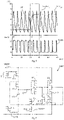
- the figure 4 represents a timing diagram obtained by simulation of the voltages ST, Vselect i , of the voltage VC1 i,j at the terminals of the capacitor C1 i,j and of the current I LED flowing in the light-emitting diode LED i,j illustrating the operation of the oscillating circuit OSC and of the display circuit 12 i,j shown in picture 3 .
- the instants t0, t1 and t2 are successive.
- the ST signal frequency is 230 kHz and the display screen refresh rate is 20 ms.
- the signal Vselect i is in the low state (0 V) from instant t0 to instant t1.
- MOS transistor T1 is therefore off and voltage VC1 i,j across capacitor C1 i,j is constant at a first level (2 V) corresponding to the last stored level of signal Data i,j . From time t1 to time t2, signal Vselect i is in the high state (12 V). MOS transistor T1 is therefore on and voltage VC1 i,j across capacitor C1 i,j changes to a second level (8 V) equal to voltage Data i,j supplied to display circuit 12 i, j . After time t2, signal Vselect i is low. MOS transistor T1 is therefore off and voltage VC1 i,j across capacitor C1 i,j remains constant at the second level.
- the current I LED flowing in the light-emitting diode LED i,j has substantially the form of a square-wave signal, alternating between a first level at approximately 12 mA and a second level at approximately 0 mA, which is periodic from instant t0 at time t1 and after time t2, with a duty cycle equal to the ratio between the duration at the first level and the duration of the period, which depends on the voltage VC1 i,j .
- the first intensity level of current I LED is determined in particular by the level of the second high reference potential and the characteristics of transistor T4.
- the oscillating circuit OSC supplies an oscillating and periodic signal ST, which preferably evolves in a substantially monotonous manner over each period.
- An embodiment of the oscillating circuit OSC is shown in picture 3 .
- any type of oscillating circuit OSC adapted to provide an oscillating and periodic signal ST, which preferably evolves in a substantially monotonous manner over each period can be used.
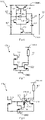
- the figure 5 represents another embodiment of the oscillating circuit OSC.
- the oscillating circuit OSC represented in figure 5 includes all the elements of the oscillating circuit OSC represented in picture 3 with the difference that the transistor T5 is connected in series with a MOS transistor T13, for example with P channel, whose first power terminal is connected to the source VREF1 of the first high reference potential and whose second power terminal is connected to the first power terminal of transistor T5 and with the difference that transistor T6 is connected in series with an N-channel MOS transistor T14, for example, the first power terminal of which is connected to the second power terminal of transistor T6 , whose second power terminal is connected to the source GND of the low reference potential and whose gate is connected to a source VREF3 of a third high reference potential.
- the oscillating circuit OSC represented in figure 5 further comprises a MOS transistor T15, for example P-channel, in series with a MOS transistor T16, for example N-channel.
- the first power terminal of the transistor T15 is connected to the source VREF1 of the first high reference potential .
- the second power terminal of transistor T15 is connected to the first power terminal of transistor T16 and the second power terminal of transistor T16 is connected to source GND of the low reference potential.
- the gate of transistor T15 is connected to the gate of transistor T13 and the gate of transistor T16 is connected to source VREF3 of the third high reference potential.
- the embodiment of the oscillating circuit OSC represented in figure 5 has the advantage of a better linearization of the charging and discharging of the capacitor C2 compared to the embodiment of the oscillating circuit OSC represented in picture 3 .
- the figure 6 represents another embodiment of the oscillating circuit OSC.
- the oscillating circuit OSC represented in figure 6 comprises two MOS transistors T17 and T18, for example P-channel transistors, the first power terminals of which are connected to the source VREF1 of the first high reference potential and the gates of which are connected to each other.
- the oscillating circuit OSC represented in figure 6 further comprises MOS transistors T19, T20 and T21, for example N-channel transistors.
- the first power terminal of transistor T19 is connected to the second power terminal of transistor T17 as well as to the gate of transistor T17.
- the first power terminal of transistor T20 is connected to the second power terminal of transistor T18.
- the first power terminal of transistor T21 is connected to the second power terminals of transistors T19 and T20.
- the second power terminal of transistor T21 is connected to the source GND of the low reference potential.
- the gate of transistor T21 is connected to a source VREF4 of a fourth high reference potential.
- the oscillating circuit OSC represented in figure 6 further includes four resistors R2, R3, R4 and R5.
- Resistor R2 is connected between source VREF1 of the first high reference potential and the gate of transistor T19.
- Resistor R3 is connected between the gate of transistor T19 and source GND of the low reference potential.
- Resistor R4 is connected between the gate of transistor T19 and the first power terminal of transistor T20.
- Resistor R5 is connected between the first power terminal of transistor T20 and the gate of transistor T20.
- the oscillating circuit OSC represented in figure 6 further comprises a capacitor C3 whose first electrode is connected to the gate of transistor T20 and whose second electrode is connected to the source GND of the low reference potential.
- the oscillating signal ST corresponds for example to the voltage across the terminals of the assembly formed by resistor R5 and capacitor C3.
- the controllable current source CS i,j supplies, when it is activated, a substantially constant current which supplies the light-emitting diode LED i,j .
- An embodiment of a controllable current source CS i,j is shown in picture 3 .
- any type of controllable current source CS i,j is suitable for supplying a substantially constant current which supplies the light-emitting diode LED i,j can be used.
- the figure 7 represents another embodiment of the controllable current source CS i,j .
- the controllable current source CS i,j represented in figure 7 comprises all the elements of the controllable current source CS i,j represented in picture 3 except that the gate of transistor T4 is connected to the gate of an N-channel MOS transistor T22, for example.
- the controllable current source CS i,j shown in figure 7 further comprises a resistor R6, one terminal of which is connected to the source VREF1 of the first high reference potential and the second terminal of which is connected to the first power terminal of the transistor T22.
- the second power terminal of transistor T22 is connected to the source GND of the low reference potential.
- the first power terminal of transistor T22 is also connected to the gate of transistor T22.
- the figure 8 represents another embodiment of the controllable current source CS i,j .
- the controllable current source CS i,j represented in figure 8 comprises MOS transistors T23, T24, T25 and T26, for example N-channel transistors.
- the first power terminal of transistor T23 is connected to the cathode of light-emitting diode LED i,j , not shown.
- the second power terminal of transistor T23 is connected to the source GND of the low reference potential.
- the first power terminal of transistor T24 is connected to the gate of transistor T23.
- the second power terminal of transistor T24 is connected to the source GND of the reference potential low.
- the first power terminal of transistor T25 is connected to the gate of transistor T23.
- the gate of transistor T25 receives the PWM signal i,j .
- the controllable current source CS i,j represented in figure 8 further comprises a resistor R7, one terminal of which is connected to the source VREF1 of the first high reference potential and the second terminal of which is connected to the first power terminal of the transistor T26.
- the second power terminal of transistor T26 is connected to the source GND of the low reference potential.
- the first power terminal of transistor T26 is also connected to the gate of transistor T26.
- the gate of transistor T26 is connected to the second power terminal of transistor T25.
- the controllable current source CS i,j represented in figure 8 further comprises an inverter INV3 whose input is connected to the gate of transistor T25 and whose output is connected to the gate of transistor T24.
- controllable current source CS i,j represented on the figures 7 or 8 can be implemented with the oscillating circuit OSC represented on the figure 5 Where 6 .
Landscapes
- Engineering & Computer Science (AREA)
- Physics & Mathematics (AREA)
- Computer Hardware Design (AREA)
- General Physics & Mathematics (AREA)
- Theoretical Computer Science (AREA)
- Control Of Indicators Other Than Cathode Ray Tubes (AREA)
- Control Of El Displays (AREA)
- Devices For Indicating Variable Information By Combining Individual Elements (AREA)
- Led Devices (AREA)
Description
- La présente demande de brevet revendique la priorité de la demande de brevet français
FR17/63313 - La présente demande concerne un écran d'affichage dont les pixels d'affichage comprennent des diodes électroluminescentes, quel que soit leur type de technologie (diode électroluminescente 2D, 3D, diode électroluminescente organique, etc...)
- Les pixels d'affichage d'un écran d'affichage à diodes électroluminescentes peuvent comprendre, pour chaque pixel d'affichage, un circuit de commande de la diode électroluminescente ou des diodes électroluminescentes du pixel d'affichage.
- Il est connu de commander une diode électroluminescente par modulation de largeur d'impulsions, appelée également PWM. Ce type de commande consiste à faire circuler des impulsions successives de courant constant dans la diode électroluminescente, les impulsions étant répétées de façon cyclique, le rapport cyclique déterminant l'intensité lumineuse émise par la diode électroluminescente. Une telle commande permet de façon avantageuse de faire fonctionner la diode électroluminescente à son point de fonctionnement optimum où l'efficacité de la diode électroluminescente, égale au rapport entre la puissance lumineuse émise par la diode électroluminescente et la puissance électrique consommée par la diode électroluminescente, est maximale.
- La tendance est à la réduction des dimensions des pixels d'affichage des écrans d'affichage à diodes électroluminescentes. Ceci entraîne une réduction de la place disponible pour la réalisation des circuits de commande des pixels d'affichage. Un inconvénient est que les circuits de commande mettant en oeuvre une modulation de largeur d'impulsions occupent généralement plus de place que d'autres types de circuits de commande. Les documents
US 2017/039935 ,US 2010/245401 ,US 7 187 355 etUS 2005/067968 décrivent chacun des écrans d'affichage dont les pixels d'affichage comprennent des diodes électroluminescentes commandées par PWM. - Un objet d'un mode de réalisation est de prévoir un écran d'affichage à diodes électroluminescentes palliant tout ou partie des inconvénients des écrans d'affichage à diodes électroluminescentes existants.
- Un autre objet d'un mode de réalisation est que les circuits de commande de l'écran d'affichage mettent en oeuvre une modulation de largeur d'impulsions.
- Un autre objet d'un mode de réalisation est que les pixels d'affichage ont des dimensions inférieures à 200 µm.
- La présente invention est exposée dans le jeu de revendications joint.
- Ces caractéristiques et avantages, ainsi que d'autres, seront exposés en détail dans la description suivante de modes de réalisation particuliers faite à titre non limitatif en relation avec les figures jointes parmi lesquelles :
- la
figure 1 représente, de façon partielle et schématique, un mode de réalisation d'un écran d'affichage ; - la
figure 2 représente un mode de réalisation plus détaillé d'une partie de l'écran d'affichage de lafigure 1 ; - la
figure 3 représente un mode de réalisation d'un circuit oscillant et d'un circuit d'affichage de l'écran d'affichage de lafigure 1 ; - la
figure 4 représente un chronogramme de signaux obtenus lors du fonctionnement du circuit oscillant et du circuit d'affichage représentés enfigure 3 ; - les
figures 5 et6 représentent d'autres modes de réalisation du circuit oscillant de lafigure 2 ; et - les
figures 7 et 8 représentent d'autres modes de réalisation de la source de courant du circuit d'affichage de lafigure 2 . - De mêmes éléments ont été désignés par de mêmes références dans les différentes figures et, de plus, les diverses figures ne sont pas tracées à l'échelle. Par souci de clarté, seuls les éléments utiles à la compréhension des modes de réalisation décrits ont été représentés et sont détaillés. Sauf précision contraire, les expressions "approximativement", "sensiblement", "environ" et "de l'ordre de" signifient à 10 % près, de préférence à 5 % près.
- De plus, on appelle "signal binaire" un signal qui alterne entre un premier état constant, par exemple un état bas, noté "0", et un deuxième état constant, par exemple un état haut, noté "1". Les états haut et bas de signaux binaires différents d'un même circuit électronique peuvent être différents. En pratique, les signaux binaires peuvent correspondre à des tensions ou à des courants qui peuvent ne pas être parfaitement constants à l'état haut ou bas. En outre, dans la suite de la description, on appelle "bornes de puissance" d'un transistor à effet de champ à grille isolée, ou transistor MOS, la source et le drain du transistor MOS. De plus, dans la présente description, on utilise le terme "relié", pour désigner soit une liaison électrique directe sans composant électronique intermédiaire, par exemple au moyen d'une piste conductrice (le terme "relié" signifiant alors "connecté") soit une liaison via un ou plusieurs composants intermédiaires (résistance, condensateur, etc.). En outre, un premier signal binaire est dit "synchrone" avec un deuxième signal binaire lorsque les fronts montants et/ou descendants du premier signal se produisent au même moment que les fronts montants et/ou descendants du deuxième signal ou se produisent à intervalles réguliers par rapport aux fronts montants et/ou descendants du deuxième signal. En particulier, des signaux binaires synchrones dérivent d'une horloge commune. Inversement, des premier et deuxième signaux binaires sont dits "asynchrones" ou "non synchrones" lorsque les fronts montants et/ou descendants du premier signal ne se produisent ni au même moment que les fronts montants et/ou descendants du deuxième signal ni à intervalles réguliers par rapport aux fronts montants et/ou descendants du deuxième signal. En particulier, des signaux binaires asynchrones ne dérivent pas d'une même horloge.
- Un pixel d'une image correspond à l'élément unitaire de l'image affichée par un écran d'affichage. Lorsque l'écran d'affichage est un écran d'affichage d'images couleur, il comprend en général pour l'affichage de chaque pixel de l'image au moins trois composants d'émission et/ou de régulation de l'intensité lumineuse, également appelées sous-pixels d'affichage, qui émettent chacun un rayonnement lumineux sensiblement dans une seule couleur (par exemple, le rouge, le vert et le bleu). La superposition des rayonnements émis par ces trois sous-pixels d'affichage fournit à l'observateur la sensation colorée correspondant au pixel de l'image affichée. Lorsque l'écran d'affichage est un écran d'affichage d'images monochromes, l'écran d'affichage comprend en général une seule source lumineuse pour l'affichage de chaque pixel de l'image.
- La
figure 1 représente, de façon partielle et schématique, un mode de réalisation d'un écran d'affichage 10. L'écran d'affichage 10 comprend des circuits d'affichage 12i,j par exemple agencés en M rangées et en N colonnes, M étant un nombre entier variant de 1 à 16000 et N étant un nombre entier variant de 1 à 8000, i étant un nombre entier variant de 1 à M et j étant un nombre entier variant de 1 à N. A titre d'exemple, enfigure 1 , M et N sont égaux à 4. Chaque circuit d'affichage 12i,j comprend un circuit de commande 14i,j et un sous-pixel d'affichage 16i,j. Chaque sous-pixel d'affichage 16i,j comprend au moins une diode électroluminescente, non représentée. - Pour chaque rangée, les circuits de commande 14i,j des circuits d'affichage 12i,j de la rangée sont reliées à une électrode de rangée 18i. Pour chaque colonne, les circuits de commande 14i,j des circuits d'affichage 12i,j de la colonne sont reliées à une électrode de colonne 20j.
- L'écran d'affichage 10 comprend un circuit de sélection 22 reliée aux électrodes de rangée 18i et adapté à fournir un signal de sélection VSelecti sur chaque électrode de rangée 18i. L'écran d'affichage 10 comprend un circuit de commande 24 reliée aux électrodes de colonne 20j et adapté à fournir un signal de données Dataj,j sur chaque électrode de colonne 20j.
- La
figure 2 représente un mode de réalisation plus détaillé de deux circuits d'affichage 12i,j et 12i+1,j de l'écran d'affichage 10. - Selon un mode de réalisation, l'écran d'affichage 10 comprend des circuits oscillants OSC de fourniture de signaux oscillants et périodiques ST reliés aux circuits d'affichage 12i,j et 12i+1,j. Chaque sous-pixel d'affichage 16i,j comprend une diode électroluminescente LEDi,j reliée en série à une source de courant commandable CSi,j. Chaque circuit de commande 14i,j comprend un circuit de mémorisation 26i,j reliée à l'électrode de rangée 18i et à l'électrode de colonne 20j. Le circuit de mémorisation 26i,j est commandé par le signal VSelecti fourni par l'électrode de rangée 18i et est adapté à stocker le signal Datai,j fourni par l'électrode de colonne 20j. Selon un mode de réalisation, le circuit de mémorisation 26i,j comprend un interrupteur SWi,j commandé par le signal VSelecti et un condensateur C1i,j. La première borne de l'interrupteur SWi,j est reliée à l'électrode de colonne 20j et la deuxième borne de l'interrupteur SWi,j est reliée à la première électrode du condensateur C1i,j, la deuxième électrode du condensateur C1i,j étant reliée à une source GND d'un potentiel de référence bas, par exemple la masse. Chaque circuit de commande 14i,j comprend, en outre, un circuit de comparaison COMPi,j relié à une première entrée (+) au circuit oscillant OSC et relié à une deuxième entrée (-) à la première électrode du condensateur C1i,j. Le circuit de comparaison COMPi,j fournit un signal PWMi,j de commande de la source de courant CSi,j.
- Un mode de réalisation d'un procédé de fonctionnement de l'écran d'affichage 10 va maintenant être décrit. Le signal Vselecti est un signal binaire. Lorsque le signal Vselecti est dans un premier état, par exemple l'état bas, l'interrupteur SWi,j est ouvert et lorsque le signal Vselecti est dans un deuxième état, par exemple l'état haut, l'interrupteur SWi,j est fermé. Les signaux Datai,j sont des signaux analogiques représentatifs des intensités lumineuses souhaitées devant être émises par les diodes électroluminescentes LEDi,j. Lorsque l'interrupteur SWi,j est fermé, la tension aux bornes du condensateur C1i,j devient sensiblement égale au signal Datai,j. Le signal PWMi,j est un signal binaire qui dépend de la comparaison entre le signal ST et la tension aux bornes du condensateur C1i,j, c'est-à-dire le signal Datai,j. A titre d'exemple, le signal PWMi,j est à un premier état, par exemple l'état haut, lorsque le signal ST est supérieur au signal Datai,j et le signal PWMi,j est à un deuxième état, par exemple l'état bas, lorsque le signal ST est inférieur au signal Datai,j. De préférence, le signal ST est un signal périodique qui, sur chaque période, croît de façon continue ou décroît de façon continue sensiblement sur la totalité de la période. A titre d'exemple, le signal ST est un signal en dents de scie qui, sur chaque période, croît ou décroît à pente sensiblement constante. Le signal PWMi,j obtenu est alors un signal cyclique modulé en largeur d'impulsions, la durée du signal PWMi,j à l'état haut sur un cycle étant proportionnelle au signal Datai,j.
- La source de courant CSi,j est commandée par le signal PMMi,j. A titre d'exemple, la source de courant CSi,j est activée, c'est-à-dire qu'elle alimente la diode électroluminescente LEDi,j en courant, lorsque le signal PWMi,j est dans le premier état, par exemple l'état haut, et la source de courant CSi,j est désactivée, c'est-à-dire que la diode électroluminescente LEDi,j n'est pas traversée par un courant, lorsque le signal PWMi,j est dans le deuxième état, par exemple l'état bas. Lorsqu'elle est activée, le courant fourni par la source de courant CSi,j est de préférence sensiblement constant et égal au courant pour lequel l'efficacité de la diode électroluminescente LEDi,j est maximale. La diode électroluminescente LEDi,j est donc soit alimentée à courant constant soit éteinte. Une commande de la diode électroluminescente LEDi,j par modulation de largeur d'impulsions est ainsi obtenue.
- Dans le mode de réalisation illustré en
figure 2 , le circuit oscillant OSC est à titre d'exemple relié à deux circuits d'affichage 12i,j et 12i+1,j, ce qui ne fait pas partie de l'invention et est présent à titre d'exemple seulement. De façon générale, l'écran d'affichage 10 comprend plusieurs circuits oscillants OSC, chaque circuit oscillant OSC étant relié à un circuit d'affichage 12i,j. L'écran d'affichage 10 comprend un circuit oscillant OSC pour chaque circuit d'affichage 12i,j. - Selon un mode de réalisation, les rangées de sous-pixels d'affichage sont activées successivement. Les signaux Vselect1 à VSelectM sont alors successivement mis à l'état haut pendant une durée ΔT, les signaux Vselect1 à VSelecti-1 et Vselecti+1 à VSelectM étant à l'état bas lorsque le signal Vselecti est à l'état haut. On appelle F la fréquence de rafraîchissement de l'écran d'affichage. La fréquence F est égale à 1/ΔT. A titre d'exemple, la fréquence F varie de 25 Hz à 120 Hz. La fréquence F' du signal ST est supérieure à 2 fois la fréquence F, de préférence supérieure à 10 fois la fréquence F, plus préférentiellement supérieure à 100 fois la fréquence F. A titre d'exemple, la fréquence F' est supérieure à 1 kHz, de préférence supérieure à 10 kHz, encore plus préférentiellement supérieure à 100 kHz. La fréquence F' du signal ST est de préférence inférieure à 1 MHz. De façon avantageuse, la structure du circuit oscillant OSC peut alors être simple. En outre, lorsque le circuit oscillant OSC met en oeuvre des interrupteurs, les pertes dues aux commutations des interrupteurs sont faibles.
- Selon un mode de réalisation, le signal ST n'est pas synchrone par rapport aux signaux VSelecti et Datai,j. Ceci signifie que le début de chaque période du signal ST n'est pas synchrone avec les instants auxquels les signaux Vselecti changent d'état. Les signaux ST fournis par les circuits oscillants OSC ne sont pas synchrones entre eux. La conception de l'écran d'affichage 10 est alors simplifiée puisqu'il n'y a pas à maintenir les signaux ST synchrones entre eux et avec les signaux VSelecti et Datai,j. En outre, les appels de courant lors du fonctionnement de l'écran d'affichage 10 sont de façon avantageuse étalés dans le temps.
- En outre, les nombre de pistes conductrices reliant le circuit oscillant OSC et le circuit de commande 14i,j associé est réduit. La distance parcourue par le signal ST entre chaque circuit oscillant OSC et le circuit d'affichage 12i,j auquel le circuit oscillant OSC est relié peut être réduite par rapport au cas où un signal d'horloge doit être fourni à chaque circuit d'affichage 12i,j.
- Les sous-pixels d'affichage 16i,j peuvent être formés sur un premier circuit électronique et les circuits de commande 14i,j et les circuits oscillants OSC peuvent être formés sur un deuxième circuit électronique, les premier et deuxième circuits électroniques étant fixés l'un à l'autre. Les circuits de commande 14i,j et les circuits oscillants OSC peuvent être formés selon une technologie CMOS. A titre de variante, les circuits de commande 14i,j et les circuits oscillants OSC peuvent être formés avec des transistors en couches minces.
- La
figure 3 représente un mode de réalisation d'un circuit oscillant OSC et d'un circuit d'affichage 12i,j de l'écran d'affichage 10 de lafigure 1 . - Dans le présent mode de réalisation, l'interrupteur SWi,j du circuit de mémorisation 26i,j du circuit de commande 14i,j correspond à un transistor MOS T1, par exemple à canal N, dont la grille reçoit le signal Vselecti, dont la première borne de puissance reçoit le signal Datai,j et dont la deuxième borne de puissance est reliée à une première électrode du condensateur C1i,j.
- Dans le présent mode de réalisation, le circuit de comparaison COMPi,j comprend un transistor MOS T2, par exemple à canal P, dont la grille est reliée à la première électrode du condensateur C1i,j, dont la première borne de puissance reçoit le signal ST et dont la deuxième borne de puissance est reliée à la source GND du potentiel de référence bas par l'intermédiaire d'une résistance R1. Le signal PWMi,j fourni par le circuit de comparaison COMPi,j correspond à la tension à la deuxième borne de puissance du transistor T2.
- Dans le présent mode de réalisation, la source de courant commandable CSi,j comprend deux transistors MOS en série T3 et T4, par exemple à canal N. La grille du transistor T3 est reliée à la deuxième borne de puissance du transistor T2. La première borne de puissance du transistor T3 est reliée à la cathode de la diode électroluminescente LEDi,j et la deuxième borne de puissance du transistor T3 est reliée à la première borne de puissance du transistor T4. La grille du transistor T3 reçoit le signal PMMi,j. L'anode de la diode électroluminescente LEDi,j est reliée à une source VREF1 d'un premier potentiel de référence haut, par exemple la tension d'alimentation de l'écran d'affichage 10. La grille du transistor T4 est reliée à une source VREF2 d'un deuxième potentiel de référence haut. La deuxième borne de puissance du transistor T4 est reliée à la source GND du potentiel de référence bas.
- Dans ce mode de réalisation, la source de courant commandable créée par les transistors T4 et T3 est conçue pour tirer un courant depuis la cathode de la LED vers la masse GND, l'anode de la LED étant connectée au potentiel haut d'alimentation VREF1. Cette structure est particulièrement adaptée à une technologie de LED dont la représentation électrique équivalente des pixels serait une structure à anode commune. L'homme de l'art pourra aisément modifier la structure de la source de courant ainsi que de son pilotage pour l'adapter à une technologie de LED/OLED dont la représentation électrique serait une structure de type cathode commune ou plus généralement une structure où la cathode de la LED serait connectée à la masse. La source de courant devrait alors être placée entre l'anode de la LED et un potentiel haut (VREF1 par exemple)
- Dans le présent mode de réalisation, le circuit oscillant OSC comprend un transistor MOS T5, par exemple à canal P, dont la première borne de puissance est reliée à la source VREF1 du premier potentiel de référence haut et dont la deuxième borne de puissance est reliée à un noeud Q fournissant le signal ST. Le circuit oscillant OSC comprend, en outre, un condensateur C2 dont la première électrode est reliée au noeud Q et dont la deuxième électrode est reliée à la source GND du potentiel de référence bas. Le circuit oscillant OSC comprend, en outre, un transistor MOS T6, par exemple à canal N, dont la première borne de puissance est reliée au noeud Q et dont la deuxième borne de puissance est reliée à la source GND du potentiel de référence bas. Le circuit oscillant OSC comprend, en outre, un premier inverseur INV1 dont l'entrée est reliée au noeud Q et dont la sortie est reliée à un noeud R. Le premier inverseur INV1 peut comprendre un transistor MOS T7, par exemple à canal P, en série avec un transistor MOS T8, par exemple à canal N. La première borne de puissance du transistor T7 est reliée à la source VREF1 du premier potentiel de référence haut et la deuxième borne de puissance du transistor T7 est reliée au noeud R. La première borne de puissance du transistor T8 est reliée au noeud R et la deuxième borne de puissance du transistor T8 est reliée à la source GND du potentiel de référence bas. Les grilles des transistors T7 et T8 sont reliées au noeud Q. Le circuit oscillant OSC comprend en outre un deuxième inverseur INV2 dont l'entrée est reliée au noeud R et dont la sortie est reliée à un noeud S. Le deuxième inverseur INV2 peut comprendre un transistor MOS T9, par exemple à canal P, en série avec un transistor MOS T10, par exemple à canal N. La première borne de puissance du transistor T9 est reliée à la source VREF1 du premier potentiel de référence haut et la deuxième borne de puissance du transistor T9 est reliée au noeud S. La première borne de puissance du transistor T10 est reliée au noeud S et la deuxième borne de puissance du transistor T10 est reliée à la source GND du potentiel de référence bas. Les grilles des transistors T9 et T10 sont reliées au noeud S. Le circuit oscillant OSC comprend, en outre, un transistor MOS T11, par exemple à canal N, dont la première borne de puissance est reliée au noeud R et dont la deuxième borne de puissance est reliée à la source GND du potentiel de référence bas et un transistor MOS T12, par exemple à canal N, dont la première borne de puissance est reliée au noeud R et dont la deuxième borne de puissance est reliée à la source GND du potentiel de référence bas. Les grilles des transistors T5, T6, T11 et T12 sont reliées au noeud S.
- Selon un mode de réalisation, la source VREF1 du premier potentiel de référence haut est commune à l'ensemble des circuits d'affichage 12i,j et des circuits oscillants OSC de l'écran d'affichage 10. Selon un mode de réalisation, la source VREF2 du deuxième potentiel de référence haut est commune à l'ensemble des circuits d'affichage 12i,j de l'écran d'affichage 10. Selon un autre mode de réalisation, l'écran d'affichage 10 comprend plusieurs sources VREF2 du deuxième potentiel de référence haut qui sont communes aux circuits d'affichage 12i,j émettant la même couleur. A titre d'exemple, l'écran d'affichage 10 comprend une première source VREF2 du deuxième potentiel de référence haut pour les circuits d'affichage 12i,j émettant de la lumière rouge, une deuxième source VREF2 du deuxième potentiel de référence haut pour les circuits d'affichage 12i,j émettant de la lumière bleue et une troisième source VREF2 du deuxième potentiel de référence haut pour les circuits d'affichage 12i,j émettant de la lumière verte. Ceci permet notamment de faire varier différemment les deuxièmes potentiels de référence haut selon la couleur de la lumière émise par les circuits d'affichage 12i,j. Selon un mode de réalisation, les sources VREF1 et VREF2 peuvent être confondues.
- Le mode de réalisation du circuit de commande 14i,j représenté en
figure 3 présente l'avantage que la structure du circuit de comparaison COMPi,j est particulièrement simple puisqu'elle ne comprend qu'un seul transistor MOS. - La
figure 4 représente un chronogramme obtenu par simulation des tensions ST, Vselecti, de la tension VC1i,j aux bornes du condensateur C1i,j et du courant ILED circulant dans la diode électroluminescente LEDi,j illustrant le fonctionnement du circuit oscillant OSC et du circuit d'affichage 12i,j représentés enfigure 3 . Les instants t0, t1 et t2 sont successifs. Dans le présent exemple, la fréquence du signal ST est de 230 kHz et la fréquence de rafraichissement de l'écran d'affichage est de 20 ms. Dans le présent exemple, le signal Vselecti est à l'état bas (0 V) de l'instant t0 à l'instant t1. Le transistor MOS T1 est donc non passant et la tension VC1i,j aux bornes du condensateur C1i,j est constante à un premier niveau (2 V) correspondant au dernier niveau mémorisé du signal Datai,j. De l'instant t1 à l'instant t2, le signal Vselecti est à l'état haut (12 V). Le transistor MOS T1 est donc passant et la tension VC1i,j aux bornes du condensateur C1i,j évolue jusqu'à un deuxième niveau (8 V) égal à la tension Datai,j fournie au circuit d'affichage 12i,j. Après l'instant t2, le signal Vselecti est à l'état bas. Le transistor MOS T1 est donc non passant et la tension VC1i,j aux bornes du condensateur C1i,j reste constante au deuxième niveau. - Le courant ILED circulant dans la diode électroluminescente LEDi,j a sensiblement la forme d'un signal en créneaux, alternant entre un premier niveau à environ 12 mA et un deuxième niveau à environ 0 mA, qui est périodique de l'instant t0 à l'instant t1 et après l'instant t2, avec un rapport cyclique, égal au rapport entre la durée au premier niveau et la durée de la période, qui dépend de la tension VC1i,j. Le premier niveau d'intensité du courant ILED est déterminé notamment par le niveau du deuxième potentiel de référence haut et les caractéristiques du transistor T4.
- Le circuit oscillant OSC fournit un signal ST oscillant et périodique, qui de préférence évolue de façon sensiblement monotone sur chaque période. Un mode de réalisation du circuit oscillant OSC est représenté en
figure 3 . Toutefois, tout type de circuit oscillant OSC adapté à fournir un signal ST oscillant et périodique, qui évolue de préférence de façon sensiblement monotone sur chaque période, peut être utilisé. - La
figure 5 représente un autre mode de réalisation du circuit oscillant OSC. - Le circuit oscillant OSC représenté en
figure 5 comprend l'ensemble des éléments du circuit oscillant OSC représenté enfigure 3 à la différence que le transistor T5 est monté en série avec un transistor MOS T13, par exemple à canal P, dont la première borne de puissance est reliée à la source VREF1 du premier potentiel de référence haut et dont la deuxième borne de puissance est reliée à la première borne de puissance du transistor T5 et à la différence que le transistor T6 est monté en série avec un transistor MOS T14, par exemple à canal N, dont la première borne de puissance est reliée à la deuxième borne de puissance du transistor T6, dont la deuxième borne de puissance est reliée à la source GND du potentiel de référence bas et dont la grille est reliée à une source VREF3 d'un troisième potentiel de référence haut. - Le circuit oscillant OSC représenté en
figure 5 comprend, en outre, un transistor MOS T15, par exemple à canal P, en série avec un transistor MOS T16, par exemple à canal N. La première borne de puissance du transistor T15 est reliée à la source VREF1 du premier potentiel de référence haut. La deuxième borne de puissance du transistor T15 est reliée à la première borne de puissance du transistor T16 et la deuxième borne de puissance du transistor T16 est reliée à la source GND du potentiel de référence bas. La grille du transistor T15 est reliée à la grille du transistor T13 et la grille du transistor T16 est reliée à la source VREF3 du troisième potentiel de référence haut. - Le mode de réalisation du circuit oscillant OSC représenté en
figure 5 présente l'avantage d'une meilleure linéarisation de la charge et de la décharge du condensateur C2 par rapport au mode de réalisation du circuit oscillant OSC représenté enfigure 3 . - La
figure 6 représente un autre mode de réalisation du circuit oscillant OSC. - Le circuit oscillant OSC représenté en
figure 6 comprend deux transistors MOS T17 et T18, par exemple à canal P, dont les premières bornes de puissance sont reliées à la source VREF1 du premier potentiel de référence haut et dont les grilles sont reliées l'une à l'autre. Le circuit oscillant OSC représenté enfigure 6 comprend, en outre, des transistors MOS T19, T20 et T21, par exemple à canal N. La première borne de puissance du transistor T19 est reliée à la deuxième borne de puissance du transistor T17 ainsi qu'à la grille du transistor T17. La première borne de puissance du transistor T20 est reliée à la deuxième borne de puissance du transistor T18. La première borne de puissance du transistor T21 est reliée aux deuxièmes bornes de puissance des transistors T19 et T20. La deuxième borne de puissance du transistor T21 est reliée à la source GND du potentiel de référence bas. La grille du transistor T21 est reliée à une source VREF4 d'un quatrième potentiel de référence haut. Le circuit oscillant OSC représenté enfigure 6 comprend, en outre, quatre résistances R2, R3, R4 et R5. La résistance R2 est reliée entre la source VREF1 du premier potentiel de référence haut et la grille du transistor T19. La résistance R3 est reliée entre la grille du transistor T19 et la source GND du potentiel de référence bas. La résistance R4 est reliée entre la grille du transistor T19 et la première borne de puissance du transistor T20. La résistance R5 est reliée entre la première borne de puissance du transistor T20 et la grille du transistor T20. Le circuit oscillant OSC représenté enfigure 6 comprend, en outre, un condensateur C3 dont la première électrode est reliée à la grille du transistor T20 et dont la deuxième électrode est reliée à la source GND du potentiel de référence bas. Le signal ST oscillant correspond par exemple à la tension aux bornes de l'ensemble formé par la résistance R5 et le condensateur C3. Un avantage du circuit oscillant OSC représenté enfigure 6 est que les instants de commutation peuvent être commandés avec une précision améliorée. - La source de courant commandable CSi,j fournit, lorsqu'elle est activée, un courant sensiblement constant qui alimente la diode électroluminescente LEDi,j. Un mode de réalisation de source de courant commandable CSi,j est représenté en
figure 3 . Toutefois, tout type de source de courant commandable CSi,j est adapté à fournir un courant sensiblement constant qui alimente la diode électroluminescente LEDi,j peut être utilisé. - La
figure 7 représente un autre mode de réalisation de la source de courant commandable CSi,j. - La source de courant commandable CSi,j représentée en
figure 7 comprend l'ensemble des éléments de la source de courant commandable CSi,j représentée enfigure 3 à la différence que la grille du transistor T4 est reliée à la grille d'un transistor MOS T22, par exemple à canal N. La source de courant commandable CSi,j représentée enfigure 7 comprend, en outre, une résistance R6 dont une borne est reliée à la source VREF1 du premier potentiel de référence haut et dont la deuxième borne est reliée à la première borne de puissance du transistor T22. La deuxième borne de puissance du transistor T22 est reliée à la source GND du potentiel de référence bas. La première borne de puissance du transistor T22 est, en outre, reliée à la grille du transistor T22. Un avantage de la source de courant représentée enfigure 7 est qu'elle ne nécessite pas l'utilisation de la source VREF2 du deuxième potentiel de référence haut. Elle peut donc facilement être réalisée au niveau du circuit d'affichage 12i,j. - La
figure 8 représente un autre mode de réalisation de la source de courant commandable CSi,j. - La source de courant commandable CSi,j représentée en
figure 8 comprend des transistors MOS T23, T24, T25 et T26, par exemple à canal N. La première borne de puissance du transistor T23 est reliée à la cathode de la diode électroluminescente LEDi,j, non représentée. La deuxième borne de puissance du transistor T23 est reliée à la source GND du potentiel de référence bas. La première borne de puissance du transistor T24 est reliée à la grille du transistor T23. La deuxième borne de puissance du transistor T24 est reliée à la source GND du potentiel de référence bas. La première borne de puissance du transistor T25 est reliée à la grille du transistor T23. La grille du transistor T25 reçoit le signal PWMi,j. La source de courant commandable CSi,j représentée enfigure 8 comprend, en outre, une résistance R7 dont une borne est reliée à la source VREF1 du premier potentiel de référence haut et dont la deuxième borne est reliée à la première borne de puissance du transistor T26. La deuxième borne de puissance du transistor T26 est reliée à la source GND du potentiel de référence bas. La première borne de puissance du transistor T26 est, en outre, reliée à la grille du transistor T26. La grille du transistor T26 est reliée à la deuxième borne de puissance du transistor T25. La source de courant commandable CSi,j représentée enfigure 8 comprend, en outre, un inverseur INV3 dont l'entrée est reliée à la grille du transistor T25 et dont la sortie est reliée à la grille du transistor T24. - Des modes de réalisation particuliers ont été décrits. Diverses modifications apparaîtront à l'homme de l'art. En outre, divers modes de réalisation avec diverses variantes ont été décrits ci-dessus. On note que divers éléments de ces divers modes de réalisation peuvent être combinés. A titre d'exemple, le mode de réalisation de la source de courant commandable CSi,j représenté sur les
figures 7 ou 8 peut être mis en oeuvre avec le circuit oscillant OSC représenté sur lesfigures 5 ou6 .
Claims (5)
- Ecran d'affichage (10) comprenant au moins mille circuits d'affichage (12i,j), chaque circuit d'affichage comprenant :- une diode électroluminescente (LEDi,j) ;- une source de courant commandable (CSi,j) alimentant la diode électroluminescente ; et- un circuit de commande (14i,j) adapté à fournir un signal (PWMi,j), modulé en largeur d'impulsions, de commande de la source de courant à partir d'un signal périodique (ST),l'écran d'affichage comprenant, en outre :- des électrodes (18i) de rangée, chacune étant reliée aux circuits de commande (14i,j) de la rangée ;- des électrodes de colonne (20j), chacune étant reliée aux circuits de commande (14i,j) de la colonne ;- un circuit (22) de sélection relié aux électrodes de rangée et adapté à fournir un signal de sélection (Vselecti) successivement sur chaque électrode de rangée (18i) ;- un circuit de fourniture (24) relié aux électrodes de colonne et adapté à fournir un signal de données (Dataj) sur chaque électrode de colonne (20j),caractérisé en que l'écran d'affichage comprend, en outre, des circuits oscillants (OSC) adaptés à fournir les signaux périodiques (ST) aux circuits de commande (14i,j), les signaux périodiques n'étant pas synchrones avec les signaux de sélection (Vselecti) des circuits d'affichage et n'étant pas synchrones entre eux, chacun desdits circuits oscillants (OSC) étant relié à un seul desdits circuits de commande (14i,j).
- Ecran d'affichage selon la revendication 1, dans lequel le circuit de commande (14i,j) de chaque circuit d'affichage (12i,j) comprend un circuit de mémorisation (26i,j) du signal de données reçu par le circuit de commande et un circuit de comparaison (COMPi,j) du signal de données et du signal périodique (ST) adapté à fournir le signal de commande (PWMi,j) modulé en largeur d'impulsions.
- Ecran d'affichage selon la revendication 1 ou 2, dans lequel la fréquence de chaque signal périodique (ST) est supérieure à deux fois la fréquence du signal de sélection (Vselecti) sur l'une des premières électrodes (18i).
- Ecran d'affichage selon l'une quelconque des revendications 1 à 3, dans lequel la fréquence de chaque signal périodique (ST) est supérieure à dix fois la fréquence du signal de sélection (Vselecti) sur l'une des premières électrodes (18i).
- Ecran d'affichage selon l'une quelconque des revendications 1 à 4, dans lequel la fréquence de chaque signal périodique (ST) est inférieure à 1 MHz.
Priority Applications (1)
| Application Number | Priority Date | Filing Date | Title |
|---|---|---|---|
| EP22157934.5A EP4020442A1 (fr) | 2017-12-28 | 2018-12-06 | Écran d'affichage à diodes électroluminescentes |
Applications Claiming Priority (2)
| Application Number | Priority Date | Filing Date | Title |
|---|---|---|---|
| FR1763313A FR3076396B1 (fr) | 2017-12-28 | 2017-12-28 | Ecran d'affichage a diodes electroluminescentes |
| PCT/EP2018/083891 WO2019129474A1 (fr) | 2017-12-28 | 2018-12-06 | Ecran d'affichage a diodes electroluminescentes |
Related Child Applications (2)
| Application Number | Title | Priority Date | Filing Date |
|---|---|---|---|
| EP22157934.5A Division EP4020442A1 (fr) | 2017-12-28 | 2018-12-06 | Écran d'affichage à diodes électroluminescentes |
| EP22157934.5A Division-Into EP4020442A1 (fr) | 2017-12-28 | 2018-12-06 | Écran d'affichage à diodes électroluminescentes |
Publications (2)
| Publication Number | Publication Date |
|---|---|
| EP3732671A1 EP3732671A1 (fr) | 2020-11-04 |
| EP3732671B1 true EP3732671B1 (fr) | 2022-05-04 |
Family
ID=61913334
Family Applications (2)
| Application Number | Title | Priority Date | Filing Date |
|---|---|---|---|
| EP22157934.5A Pending EP4020442A1 (fr) | 2017-12-28 | 2018-12-06 | Écran d'affichage à diodes électroluminescentes |
| EP18811319.5A Active EP3732671B1 (fr) | 2017-12-28 | 2018-12-06 | Écran d'affichage à diodes électroluminescentes |
Family Applications Before (1)
| Application Number | Title | Priority Date | Filing Date |
|---|---|---|---|
| EP22157934.5A Pending EP4020442A1 (fr) | 2017-12-28 | 2018-12-06 | Écran d'affichage à diodes électroluminescentes |
Country Status (8)
| Country | Link |
|---|---|
| US (1) | US11443686B2 (fr) |
| EP (2) | EP4020442A1 (fr) |
| JP (1) | JP7223009B2 (fr) |
| KR (1) | KR102607953B1 (fr) |
| CN (1) | CN111527537B (fr) |
| FR (1) | FR3076396B1 (fr) |
| TW (1) | TWI780276B (fr) |
| WO (1) | WO2019129474A1 (fr) |
Families Citing this family (3)
| Publication number | Priority date | Publication date | Assignee | Title |
|---|---|---|---|---|
| US11710445B2 (en) * | 2019-01-24 | 2023-07-25 | Google Llc | Backplane configurations and operations |
| FR3120988B1 (fr) | 2021-03-18 | 2023-03-24 | Commissariat Energie Atomique | Dispositif d'affichage émissif à LED |
| FR3137485B1 (fr) * | 2022-06-29 | 2024-12-06 | Aledia | Pixel d'affichage comprenant des sources électroluminescentes |
Family Cites Families (13)
| Publication number | Priority date | Publication date | Assignee | Title |
|---|---|---|---|---|
| GB2367413A (en) | 2000-09-28 | 2002-04-03 | Seiko Epson Corp | Organic electroluminescent display device |
| KR100513318B1 (ko) | 2003-06-24 | 2005-09-09 | 삼성전기주식회사 | 비동기 pwm 구동방식의 lcd 패널용 백라이트 인버터 |
| JP3935891B2 (ja) * | 2003-09-29 | 2007-06-27 | 三洋電機株式会社 | ランプ電圧発生装置及びアクティブマトリクス駆動型表示装置 |
| US20080100224A1 (en) * | 2006-10-31 | 2008-05-01 | Felder Matthew D | System on a chip with backlight controller |
| GB2453375A (en) * | 2007-10-05 | 2009-04-08 | Cambridge Display Tech Ltd | Driving a display using an effective analogue drive signal generated from a modulated digital signal |
| TW201106798A (en) * | 2009-08-12 | 2011-02-16 | Novatek Microelectronics Corp | Light emitting diode module and driving method thereof |
| JP5595126B2 (ja) * | 2010-06-03 | 2014-09-24 | ローム株式会社 | Led駆動装置およびこれを備えた電子機器 |
| KR101712676B1 (ko) * | 2011-02-18 | 2017-03-07 | 매그나칩 반도체 유한회사 | Pwm 제어 회로 및 이를 이용한 led 구동회로 |
| US8803445B2 (en) * | 2012-09-07 | 2014-08-12 | Infineon Technologies Austria Ag | Circuit and method for driving LEDs |
| JP6157178B2 (ja) * | 2013-04-01 | 2017-07-05 | ソニーセミコンダクタソリューションズ株式会社 | 表示装置 |
| US10186187B2 (en) * | 2015-03-16 | 2019-01-22 | Apple Inc. | Organic light-emitting diode display with pulse-width-modulated brightness control |
| JP2016212239A (ja) | 2015-05-08 | 2016-12-15 | ソニー株式会社 | 表示装置、表示方法、および電子機器 |
| TW201706978A (zh) * | 2015-08-04 | 2017-02-16 | 啟耀光電股份有限公司 | 顯示面板和畫素電路 |
-
2017
- 2017-12-28 FR FR1763313A patent/FR3076396B1/fr active Active
-
2018
- 2018-12-06 WO PCT/EP2018/083891 patent/WO2019129474A1/fr not_active Ceased
- 2018-12-06 KR KR1020207016742A patent/KR102607953B1/ko active Active
- 2018-12-06 EP EP22157934.5A patent/EP4020442A1/fr active Pending
- 2018-12-06 US US16/766,636 patent/US11443686B2/en active Active
- 2018-12-06 JP JP2020535179A patent/JP7223009B2/ja active Active
- 2018-12-06 EP EP18811319.5A patent/EP3732671B1/fr active Active
- 2018-12-06 CN CN201880084383.1A patent/CN111527537B/zh active Active
- 2018-12-10 TW TW107144301A patent/TWI780276B/zh active
Also Published As
| Publication number | Publication date |
|---|---|
| US20200365075A1 (en) | 2020-11-19 |
| US11443686B2 (en) | 2022-09-13 |
| JP7223009B2 (ja) | 2023-02-15 |
| KR20200094753A (ko) | 2020-08-07 |
| WO2019129474A1 (fr) | 2019-07-04 |
| CN111527537A (zh) | 2020-08-11 |
| TWI780276B (zh) | 2022-10-11 |
| FR3076396B1 (fr) | 2021-12-03 |
| KR102607953B1 (ko) | 2023-11-29 |
| TW201931348A (zh) | 2019-08-01 |
| EP4020442A1 (fr) | 2022-06-29 |
| CN111527537B (zh) | 2023-06-27 |
| EP3732671A1 (fr) | 2020-11-04 |
| FR3076396A1 (fr) | 2019-07-05 |
| JP2021508847A (ja) | 2021-03-11 |
Similar Documents
| Publication | Publication Date | Title |
|---|---|---|
| KR102281222B1 (ko) | 하이브리드 픽셀 내 및 외부 보상을 갖는 전자 디스플레이 | |
| CN110322829B (zh) | 发光二极管的脉宽调制控制 | |
| KR102629873B1 (ko) | 표시 장치 | |
| US8384631B2 (en) | Method and device for driving an active matrix display panel | |
| US9336897B2 (en) | Shift register circuit | |
| CN100561555C (zh) | 电子电路、电光学装置及驱动方法、电子元件的控制方法 | |
| JP4626660B2 (ja) | 電気光学装置、電子機器、及び電気光学装置の駆動方法 | |
| EP4020442A1 (fr) | Écran d'affichage à diodes électroluminescentes | |
| JP2005017979A (ja) | 電流生成供給回路及びその制御方法並びに該電流生成供給回路を備えた表示装置 | |
| EP2278696A1 (fr) | Convertisseur élévateur-inverseur et son procédé de commande | |
| US20110080441A1 (en) | Method of driving an organic light emitting diode (oled) pixel, a system for driving an oled pixel and a computer-readable medium | |
| CN103383832A (zh) | 显示装置、显示装置的驱动方法以及电子设备 | |
| KR101746634B1 (ko) | 시프트 레지스터 유닛, 시프트 레지스터, 게이트 구동 회로 및 디스플레이 장치 | |
| WO2016027425A1 (fr) | Dispositif d'affichage et procédé de commande associé | |
| JP4232193B2 (ja) | 電流生成供給回路及び電流生成供給回路を備えた表示装置 | |
| WO2023117605A1 (fr) | Ecran d'affichage comprenant des pixels d'affichage a diodes electroluminescentes | |
| US20250316209A1 (en) | Display pixel comprising light-emitting diodes and display screen having such display pixels | |
| KR102333142B1 (ko) | 화소 및 상기 화소를 포함하는 유기발광 표시장치 | |
| CN107331339B (zh) | 显示装置及其控制方法 | |
| JP4103139B2 (ja) | 電流生成供給回路及び該電流生成供給回路を備えた表示装置 | |
| JP4941426B2 (ja) | 表示装置 | |
| FR3140471A1 (fr) | Dispositif optoélectronique | |
| JP2007322795A (ja) | 発光ダイオード駆動回路およびそれを使用した表示装置 | |
| FR3150040A1 (fr) | Pixel d'affichage comprenant des diodes électroluminescentes pour un écran d'affichage | |
| FR3136883A1 (fr) | Pixel d'affichage comprenant des sources électroluminescentes |
Legal Events
| Date | Code | Title | Description |
|---|---|---|---|
| STAA | Information on the status of an ep patent application or granted ep patent |
Free format text: STATUS: UNKNOWN |
|
| STAA | Information on the status of an ep patent application or granted ep patent |
Free format text: STATUS: THE INTERNATIONAL PUBLICATION HAS BEEN MADE |
|
| PUAI | Public reference made under article 153(3) epc to a published international application that has entered the european phase |
Free format text: ORIGINAL CODE: 0009012 |
|
| STAA | Information on the status of an ep patent application or granted ep patent |
Free format text: STATUS: REQUEST FOR EXAMINATION WAS MADE |
|
| 17P | Request for examination filed |
Effective date: 20200515 |
|
| AK | Designated contracting states |
Kind code of ref document: A1 Designated state(s): AL AT BE BG CH CY CZ DE DK EE ES FI FR GB GR HR HU IE IS IT LI LT LU LV MC MK MT NL NO PL PT RO RS SE SI SK SM TR |
|
| AX | Request for extension of the european patent |
Extension state: BA ME |
|
| RAP1 | Party data changed (applicant data changed or rights of an application transferred) |
Owner name: ALEDIA |
|
| DAV | Request for validation of the european patent (deleted) | ||
| DAX | Request for extension of the european patent (deleted) | ||
| STAA | Information on the status of an ep patent application or granted ep patent |
Free format text: STATUS: EXAMINATION IS IN PROGRESS |
|
| 17Q | First examination report despatched |
Effective date: 20211011 |
|
| GRAP | Despatch of communication of intention to grant a patent |
Free format text: ORIGINAL CODE: EPIDOSNIGR1 |
|
| STAA | Information on the status of an ep patent application or granted ep patent |
Free format text: STATUS: GRANT OF PATENT IS INTENDED |
|
| INTG | Intention to grant announced |
Effective date: 20211203 |
|
| GRAS | Grant fee paid |
Free format text: ORIGINAL CODE: EPIDOSNIGR3 |
|
| GRAA | (expected) grant |
Free format text: ORIGINAL CODE: 0009210 |
|
| STAA | Information on the status of an ep patent application or granted ep patent |
Free format text: STATUS: THE PATENT HAS BEEN GRANTED |
|
| AK | Designated contracting states |
Kind code of ref document: B1 Designated state(s): AL AT BE BG CH CY CZ DE DK EE ES FI FR GB GR HR HU IE IS IT LI LT LU LV MC MK MT NL NO PL PT RO RS SE SI SK SM TR |
|
| REG | Reference to a national code |
Ref country code: GB Ref legal event code: FG4D Free format text: NOT ENGLISH |
|
| REG | Reference to a national code |
Ref country code: CH Ref legal event code: EP |
|
| REG | Reference to a national code |
Ref country code: AT Ref legal event code: REF Ref document number: 1489951 Country of ref document: AT Kind code of ref document: T Effective date: 20220515 |
|
| REG | Reference to a national code |
Ref country code: IE Ref legal event code: FG4D Free format text: LANGUAGE OF EP DOCUMENT: FRENCH Ref country code: DE Ref legal event code: R096 Ref document number: 602018035098 Country of ref document: DE |
|
| REG | Reference to a national code |
Ref country code: LT Ref legal event code: MG9D |
|
| REG | Reference to a national code |
Ref country code: NL Ref legal event code: MP Effective date: 20220504 |
|
| REG | Reference to a national code |
Ref country code: AT Ref legal event code: MK05 Ref document number: 1489951 Country of ref document: AT Kind code of ref document: T Effective date: 20220504 |
|
| PG25 | Lapsed in a contracting state [announced via postgrant information from national office to epo] |
Ref country code: SE Free format text: LAPSE BECAUSE OF FAILURE TO SUBMIT A TRANSLATION OF THE DESCRIPTION OR TO PAY THE FEE WITHIN THE PRESCRIBED TIME-LIMIT Effective date: 20220504 Ref country code: PT Free format text: LAPSE BECAUSE OF FAILURE TO SUBMIT A TRANSLATION OF THE DESCRIPTION OR TO PAY THE FEE WITHIN THE PRESCRIBED TIME-LIMIT Effective date: 20220905 Ref country code: NO Free format text: LAPSE BECAUSE OF FAILURE TO SUBMIT A TRANSLATION OF THE DESCRIPTION OR TO PAY THE FEE WITHIN THE PRESCRIBED TIME-LIMIT Effective date: 20220804 Ref country code: NL Free format text: LAPSE BECAUSE OF FAILURE TO SUBMIT A TRANSLATION OF THE DESCRIPTION OR TO PAY THE FEE WITHIN THE PRESCRIBED TIME-LIMIT Effective date: 20220504 Ref country code: LT Free format text: LAPSE BECAUSE OF FAILURE TO SUBMIT A TRANSLATION OF THE DESCRIPTION OR TO PAY THE FEE WITHIN THE PRESCRIBED TIME-LIMIT Effective date: 20220504 Ref country code: HR Free format text: LAPSE BECAUSE OF FAILURE TO SUBMIT A TRANSLATION OF THE DESCRIPTION OR TO PAY THE FEE WITHIN THE PRESCRIBED TIME-LIMIT Effective date: 20220504 Ref country code: GR Free format text: LAPSE BECAUSE OF FAILURE TO SUBMIT A TRANSLATION OF THE DESCRIPTION OR TO PAY THE FEE WITHIN THE PRESCRIBED TIME-LIMIT Effective date: 20220805 Ref country code: FI Free format text: LAPSE BECAUSE OF FAILURE TO SUBMIT A TRANSLATION OF THE DESCRIPTION OR TO PAY THE FEE WITHIN THE PRESCRIBED TIME-LIMIT Effective date: 20220504 Ref country code: BG Free format text: LAPSE BECAUSE OF FAILURE TO SUBMIT A TRANSLATION OF THE DESCRIPTION OR TO PAY THE FEE WITHIN THE PRESCRIBED TIME-LIMIT Effective date: 20220804 Ref country code: AT Free format text: LAPSE BECAUSE OF FAILURE TO SUBMIT A TRANSLATION OF THE DESCRIPTION OR TO PAY THE FEE WITHIN THE PRESCRIBED TIME-LIMIT Effective date: 20220504 |
|
| PG25 | Lapsed in a contracting state [announced via postgrant information from national office to epo] |
Ref country code: RS Free format text: LAPSE BECAUSE OF FAILURE TO SUBMIT A TRANSLATION OF THE DESCRIPTION OR TO PAY THE FEE WITHIN THE PRESCRIBED TIME-LIMIT Effective date: 20220504 Ref country code: PL Free format text: LAPSE BECAUSE OF FAILURE TO SUBMIT A TRANSLATION OF THE DESCRIPTION OR TO PAY THE FEE WITHIN THE PRESCRIBED TIME-LIMIT Effective date: 20220504 Ref country code: LV Free format text: LAPSE BECAUSE OF FAILURE TO SUBMIT A TRANSLATION OF THE DESCRIPTION OR TO PAY THE FEE WITHIN THE PRESCRIBED TIME-LIMIT Effective date: 20220504 Ref country code: IS Free format text: LAPSE BECAUSE OF FAILURE TO SUBMIT A TRANSLATION OF THE DESCRIPTION OR TO PAY THE FEE WITHIN THE PRESCRIBED TIME-LIMIT Effective date: 20220904 |
|
| PG25 | Lapsed in a contracting state [announced via postgrant information from national office to epo] |
Ref country code: SM Free format text: LAPSE BECAUSE OF FAILURE TO SUBMIT A TRANSLATION OF THE DESCRIPTION OR TO PAY THE FEE WITHIN THE PRESCRIBED TIME-LIMIT Effective date: 20220504 Ref country code: SK Free format text: LAPSE BECAUSE OF FAILURE TO SUBMIT A TRANSLATION OF THE DESCRIPTION OR TO PAY THE FEE WITHIN THE PRESCRIBED TIME-LIMIT Effective date: 20220504 Ref country code: RO Free format text: LAPSE BECAUSE OF FAILURE TO SUBMIT A TRANSLATION OF THE DESCRIPTION OR TO PAY THE FEE WITHIN THE PRESCRIBED TIME-LIMIT Effective date: 20220504 Ref country code: ES Free format text: LAPSE BECAUSE OF FAILURE TO SUBMIT A TRANSLATION OF THE DESCRIPTION OR TO PAY THE FEE WITHIN THE PRESCRIBED TIME-LIMIT Effective date: 20220504 Ref country code: EE Free format text: LAPSE BECAUSE OF FAILURE TO SUBMIT A TRANSLATION OF THE DESCRIPTION OR TO PAY THE FEE WITHIN THE PRESCRIBED TIME-LIMIT Effective date: 20220504 Ref country code: DK Free format text: LAPSE BECAUSE OF FAILURE TO SUBMIT A TRANSLATION OF THE DESCRIPTION OR TO PAY THE FEE WITHIN THE PRESCRIBED TIME-LIMIT Effective date: 20220504 Ref country code: CZ Free format text: LAPSE BECAUSE OF FAILURE TO SUBMIT A TRANSLATION OF THE DESCRIPTION OR TO PAY THE FEE WITHIN THE PRESCRIBED TIME-LIMIT Effective date: 20220504 |
|
| REG | Reference to a national code |
Ref country code: DE Ref legal event code: R097 Ref document number: 602018035098 Country of ref document: DE |
|
| PLBE | No opposition filed within time limit |
Free format text: ORIGINAL CODE: 0009261 |
|
| STAA | Information on the status of an ep patent application or granted ep patent |
Free format text: STATUS: NO OPPOSITION FILED WITHIN TIME LIMIT |
|
| PG25 | Lapsed in a contracting state [announced via postgrant information from national office to epo] |
Ref country code: AL Free format text: LAPSE BECAUSE OF FAILURE TO SUBMIT A TRANSLATION OF THE DESCRIPTION OR TO PAY THE FEE WITHIN THE PRESCRIBED TIME-LIMIT Effective date: 20220504 |
|
| 26N | No opposition filed |
Effective date: 20230207 |
|
| PG25 | Lapsed in a contracting state [announced via postgrant information from national office to epo] |
Ref country code: SI Free format text: LAPSE BECAUSE OF FAILURE TO SUBMIT A TRANSLATION OF THE DESCRIPTION OR TO PAY THE FEE WITHIN THE PRESCRIBED TIME-LIMIT Effective date: 20220504 |
|
| REG | Reference to a national code |
Ref country code: CH Ref legal event code: PL |
|
| REG | Reference to a national code |
Ref country code: BE Ref legal event code: MM Effective date: 20221231 |
|
| PG25 | Lapsed in a contracting state [announced via postgrant information from national office to epo] |
Ref country code: LU Free format text: LAPSE BECAUSE OF NON-PAYMENT OF DUE FEES Effective date: 20221206 |
|
| PG25 | Lapsed in a contracting state [announced via postgrant information from national office to epo] |
Ref country code: LI Free format text: LAPSE BECAUSE OF NON-PAYMENT OF DUE FEES Effective date: 20221231 Ref country code: IE Free format text: LAPSE BECAUSE OF NON-PAYMENT OF DUE FEES Effective date: 20221206 Ref country code: CH Free format text: LAPSE BECAUSE OF NON-PAYMENT OF DUE FEES Effective date: 20221231 |
|
| PG25 | Lapsed in a contracting state [announced via postgrant information from national office to epo] |
Ref country code: BE Free format text: LAPSE BECAUSE OF NON-PAYMENT OF DUE FEES Effective date: 20221231 |
|
| PG25 | Lapsed in a contracting state [announced via postgrant information from national office to epo] |
Ref country code: IT Free format text: LAPSE BECAUSE OF FAILURE TO SUBMIT A TRANSLATION OF THE DESCRIPTION OR TO PAY THE FEE WITHIN THE PRESCRIBED TIME-LIMIT Effective date: 20220504 |
|
| PG25 | Lapsed in a contracting state [announced via postgrant information from national office to epo] |
Ref country code: CY Free format text: LAPSE BECAUSE OF FAILURE TO SUBMIT A TRANSLATION OF THE DESCRIPTION OR TO PAY THE FEE WITHIN THE PRESCRIBED TIME-LIMIT Effective date: 20220504 |
|
| PG25 | Lapsed in a contracting state [announced via postgrant information from national office to epo] |
Ref country code: MK Free format text: LAPSE BECAUSE OF FAILURE TO SUBMIT A TRANSLATION OF THE DESCRIPTION OR TO PAY THE FEE WITHIN THE PRESCRIBED TIME-LIMIT Effective date: 20220504 Ref country code: HU Free format text: LAPSE BECAUSE OF FAILURE TO SUBMIT A TRANSLATION OF THE DESCRIPTION OR TO PAY THE FEE WITHIN THE PRESCRIBED TIME-LIMIT; INVALID AB INITIO Effective date: 20181206 |
|
| PG25 | Lapsed in a contracting state [announced via postgrant information from national office to epo] |
Ref country code: MC Free format text: LAPSE BECAUSE OF FAILURE TO SUBMIT A TRANSLATION OF THE DESCRIPTION OR TO PAY THE FEE WITHIN THE PRESCRIBED TIME-LIMIT Effective date: 20220504 |
|
| PG25 | Lapsed in a contracting state [announced via postgrant information from national office to epo] |
Ref country code: TR Free format text: LAPSE BECAUSE OF FAILURE TO SUBMIT A TRANSLATION OF THE DESCRIPTION OR TO PAY THE FEE WITHIN THE PRESCRIBED TIME-LIMIT Effective date: 20220504 Ref country code: MC Free format text: LAPSE BECAUSE OF FAILURE TO SUBMIT A TRANSLATION OF THE DESCRIPTION OR TO PAY THE FEE WITHIN THE PRESCRIBED TIME-LIMIT Effective date: 20220504 |
|
| PG25 | Lapsed in a contracting state [announced via postgrant information from national office to epo] |
Ref country code: MT Free format text: LAPSE BECAUSE OF FAILURE TO SUBMIT A TRANSLATION OF THE DESCRIPTION OR TO PAY THE FEE WITHIN THE PRESCRIBED TIME-LIMIT Effective date: 20220504 |
|
| PG25 | Lapsed in a contracting state [announced via postgrant information from national office to epo] |
Ref country code: BG Free format text: LAPSE BECAUSE OF FAILURE TO SUBMIT A TRANSLATION OF THE DESCRIPTION OR TO PAY THE FEE WITHIN THE PRESCRIBED TIME-LIMIT Effective date: 20220504 |
|
| PG25 | Lapsed in a contracting state [announced via postgrant information from national office to epo] |
Ref country code: BG Free format text: LAPSE BECAUSE OF FAILURE TO SUBMIT A TRANSLATION OF THE DESCRIPTION OR TO PAY THE FEE WITHIN THE PRESCRIBED TIME-LIMIT Effective date: 20220504 |
|
| PGFP | Annual fee paid to national office [announced via postgrant information from national office to epo] |
Ref country code: DE Payment date: 20251211 Year of fee payment: 8 |
|
| PGFP | Annual fee paid to national office [announced via postgrant information from national office to epo] |
Ref country code: GB Payment date: 20251219 Year of fee payment: 8 |
|
| PGFP | Annual fee paid to national office [announced via postgrant information from national office to epo] |
Ref country code: FR Payment date: 20251229 Year of fee payment: 8 |