EP3731422B1 - Ic chip - Google Patents
Ic chip Download PDFInfo
- Publication number
- EP3731422B1 EP3731422B1 EP18892943.4A EP18892943A EP3731422B1 EP 3731422 B1 EP3731422 B1 EP 3731422B1 EP 18892943 A EP18892943 A EP 18892943A EP 3731422 B1 EP3731422 B1 EP 3731422B1
- Authority
- EP
- European Patent Office
- Prior art keywords
- reception
- chip
- circuit
- input unit
- arrangement
- Prior art date
- Legal status (The legal status is an assumption and is not a legal conclusion. Google has not performed a legal analysis and makes no representation as to the accuracy of the status listed.)
- Active
Links
- 230000005540 biological transmission Effects 0.000 claims description 64
- 239000003990 capacitor Substances 0.000 claims description 51
- 238000010586 diagram Methods 0.000 description 43
- ATJFFYVFTNAWJD-UHFFFAOYSA-N Tin Chemical compound [Sn] ATJFFYVFTNAWJD-UHFFFAOYSA-N 0.000 description 8
- 229910052718 tin Inorganic materials 0.000 description 8
- 239000008186 active pharmaceutical agent Substances 0.000 description 5
- 230000015556 catabolic process Effects 0.000 description 5
- 238000006731 degradation reaction Methods 0.000 description 5
- 230000000694 effects Effects 0.000 description 4
- 230000003071 parasitic effect Effects 0.000 description 4
- 238000004088 simulation Methods 0.000 description 3
- 238000004891 communication Methods 0.000 description 2
- 238000000034 method Methods 0.000 description 2
- 238000012546 transfer Methods 0.000 description 2
- 230000000903 blocking effect Effects 0.000 description 1
- 230000001427 coherent effect Effects 0.000 description 1
- 230000000593 degrading effect Effects 0.000 description 1
- 230000001419 dependent effect Effects 0.000 description 1
- 238000004100 electronic packaging Methods 0.000 description 1
- 238000011156 evaluation Methods 0.000 description 1
- 230000005669 field effect Effects 0.000 description 1
- 238000003780 insertion Methods 0.000 description 1
- 230000037431 insertion Effects 0.000 description 1
- 238000004519 manufacturing process Methods 0.000 description 1
- 230000003287 optical effect Effects 0.000 description 1
- 239000004065 semiconductor Substances 0.000 description 1
- 230000008054 signal transmission Effects 0.000 description 1
- 230000008685 targeting Effects 0.000 description 1
Images


Classifications
-
- H—ELECTRICITY
- H02—GENERATION; CONVERSION OR DISTRIBUTION OF ELECTRIC POWER
- H02H—EMERGENCY PROTECTIVE CIRCUIT ARRANGEMENTS
- H02H9/00—Emergency protective circuit arrangements for limiting excess current or voltage without disconnection
- H02H9/04—Emergency protective circuit arrangements for limiting excess current or voltage without disconnection responsive to excess voltage
- H02H9/045—Emergency protective circuit arrangements for limiting excess current or voltage without disconnection responsive to excess voltage adapted to a particular application and not provided for elsewhere
- H02H9/046—Emergency protective circuit arrangements for limiting excess current or voltage without disconnection responsive to excess voltage adapted to a particular application and not provided for elsewhere responsive to excess voltage appearing at terminals of integrated circuits
-
- H—ELECTRICITY
- H01—ELECTRIC ELEMENTS
- H01L—SEMICONDUCTOR DEVICES NOT COVERED BY CLASS H10
- H01L23/00—Details of semiconductor or other solid state devices
- H01L23/58—Structural electrical arrangements for semiconductor devices not otherwise provided for, e.g. in combination with batteries
- H01L23/60—Protection against electrostatic charges or discharges, e.g. Faraday shields
-
- H—ELECTRICITY
- H01—ELECTRIC ELEMENTS
- H01L—SEMICONDUCTOR DEVICES NOT COVERED BY CLASS H10
- H01L23/00—Details of semiconductor or other solid state devices
- H01L23/58—Structural electrical arrangements for semiconductor devices not otherwise provided for, e.g. in combination with batteries
- H01L23/64—Impedance arrangements
-
- H—ELECTRICITY
- H03—ELECTRONIC CIRCUITRY
- H03H—IMPEDANCE NETWORKS, e.g. RESONANT CIRCUITS; RESONATORS
- H03H7/00—Multiple-port networks comprising only passive electrical elements as network components
- H03H7/01—Frequency selective two-port networks
- H03H7/0138—Electrical filters or coupling circuits
-
- H—ELECTRICITY
- H04—ELECTRIC COMMUNICATION TECHNIQUE
- H04B—TRANSMISSION
- H04B3/00—Line transmission systems
- H04B3/02—Details
Definitions
- the present invention relates to an IC chip which includes a compact wideband DC-blocking circuit.
- the ICs When high-speed electrical signal communication is performed between ICs (Integrated Circuits), the ICs are generally connected by a transmission line (transmission medium) in which a characteristic impedance Z0 is 50 ⁇ .
- a 50- ⁇ resistor for impedance matching is arranged on each of the transmission-end side and the reception-end side of the transmission line.
- a DC-blocking capacitor that cuts off the DC component of a signal is arranged between the ICs.
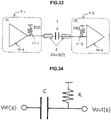
- Fig. 33 shows an example of a general signal transmission/reception arrangement which includes a DC-blocking capacitor.
- a transmission-side circuit 10-1 and a 50- ⁇ resistor 11-1 for impedance matching are arranged in a transmission-side IC 1-1
- a reception-side circuit 10-2 and a 50- ⁇ resistor 11-2 for impedance matching are arranged in a transmission-side IC 1-2.
- the IC 1-1 and the IC 1-2 are connected by a transmission line 101, and a DC-blocking capacitor 3 is arranged in the middle of the transmission line 101.
- the capacitor C needs to be set to about 5 nF or more (nF order) to implement a cutoff frequency of about 1 MHz. It is difficult, in terms of the dedicated area, to manufacture an nF-order capacitor on a chip by a general semiconductor process, and a DC-blocking capacitor needs to be mounted externally (off the chip) (see non-patent literature 1).
- US 2013/002347 A1 discloses an integrated circuit according to the preamble of claim 1.
- Non-Patent Literature 1 H. Wakita, et al., "36-GHz-Bandwidth Quad-channel Driver Module using Compact QFN Package for Optical Coherent Systems", Electrical Performance of Electronic Packaging and Systems (EPEPS), 2015
- the present invention has been made to solve the above-described problem and has as its object to implement a compact wideband DC-blocking circuit that can be mounted on an IC chip while ensuring impedance matching.
- the present application discloses a IC chip comprising: a pad (15) connected to a first transmission line (2) outside the chip; a signal line (16), one end of which is connected to the pad; a termination resistor (11) connected to the other end of the signal line and configured to terminate the first transmission line; a reception-side input unit circuit (10) configured to receive a signal transmitted from a transmission-side via the first transmission line; and a capacitor (12) inserted between a node (A) of the signal line and the termination resistor and an input terminal of the reception-side input unit circuit, characterized in that a length (L) from the node of the signal line and the termination resistor to the input terminal of the reception-side input unit circuit is shorter than a wavelength of a maximum frequency component of a signal handled by the reception-side input unit circuit.
- the present invention provides a compact wideband DC-blocking circuit that can be mounted on an IC chip while ensuring 50- ⁇ impedance matching.
- a blocking capacitor which is conventionally arranged on a transmission line between a transmission-side IC chip and a reception-side IC chip, is arranged on the reception-side IC chip.
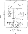
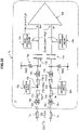
- FIG. 1 is a circuit diagram showing a reception-side IC chip according to the first embodiment of the present invention.
- a reception-side IC chip 1a at least includes a pad 15 connected to a transmission line 2 whose characteristic impedance Z0 from outside the chip is 50 ⁇ , a signal line 16, one end of which is connected to the pad 15, a reception-side input unit circuit 10 that receives a signal S transmitted from a transmission-side IC chip (not shown) via the transmission line 2, a 50- ⁇ termination resistor 11 for impedance matching that is connected between a predetermined voltage and the other end of the signal line 16 and terminates the transmission line 2, and a capacitor 12 inserted between a node A of the signal line 16 and the termination resistor 11 and an input terminal In of the reception-side input unit circuit 10.
- an on-chip DC-blocking circuit is formed by the capacitor 12.
- an input impedance Zin of the reception-side input unit circuit 10 needs to be increased to make the capacitor 12 be of a size that can be mounted on a chip.
- the degree to which the input impedance Zin is to be set will be described later.
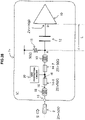
- FIG. 2 is a circuit diagram showing the arrangement of a reception-side IC chip according to the second embodiment of the present invention.
- a reception-side IC chip 1b according to this embodiment has the same arrangement as the first embodiment, but is characterized in that a length L from a node A of a signal line 16 and a termination resistor 11 to an input terminal In of a reception-side input unit circuit 10 is sufficiently shorter than the wavelength of a maximum frequency component of a signal S handled by the reception-side IC chip 1b (reception-side input unit circuit 10).
- the length L can be set to be less than 1/20 of the wavelength of the maximum frequency component of the signal S handled by the reception-side IC chip 1b (reception-side input unit circuit 10).
- a circuit whose length L is of a size less than 1/20 of a signal wavelength can be handled as a lumped constant circuit. That is, as long as the size is less than 1/20 of the signal wavelength, the signal waveform will not be influenced even under a state in which a reflected wave or the like will occur.
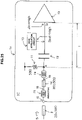
- FIG. 3 is a circuit diagram showing the arrangement of a reception-side IC chip according to the third embodiment of the present invention.
- a reception-side IC chip 1c according to this embodiment is obtained by adding, to the arrangement of the first embodiment, a bias application circuit 13 that applies a DC bias voltage to an input terminal In of a reception-side input unit circuit 10.
- an input impedance Zin of the reception-side input unit circuit 10 and an output impedance Zout of the bias application circuit 13 need to be increased.
- the degrees to which the input impedance Zin and the output impedance Zout are to be set will be described later.
- FIG. 4 is a circuit diagram showing the arrangement of a reception-side IC chip according to the fourth embodiment of the present invention.
- a reception-side IC chip 1d according to this embodiment has the same arrangement as the third embodiment, but is characterized in that a length L from a node A of a signal line 16 and a termination resistor 11 to an input terminal In of a reception-side input unit circuit 10 is sufficiently shorter than the wavelength of a maximum frequency component of a signal S handled by the reception-side IC chip 1d (reception-side input unit circuit 10).
- the length L can be set to be less than 1/20 of the wavelength of the maximum frequency component of the signal S handled by the reception-side IC chip 1d (reception-side input unit circuit 10).
- a DC-blocking circuit arrangement that has the characteristics described in the first to fourth embodiments, impedance matching by the 50- ⁇ termination resistor 11 arranged before a capacitor 12 can be ensured and a resistance value R, as indicated in the circuit shown in Fig. 34 , can be designed to be sufficiently large when the reception-side input unit circuit 10 is viewed from the node A of the signal line 16 and the termination resistor 11. As a result, the cutoff frequency of a high-pass filter can be extended to a low frequency range even if the value of the capacitor 12 is reduced.
- a high-pass filter is formed by the capacitor 12 and an input impedance Zin of the reception-side input unit circuit 10.
- the input impedance Zin (the value of the resistor R) can be set based on equation (1) so that the cutoff frequency of the high-pass filter and the capacitance of the capacitor 12 become desired values, respectively.
- a high-pass filter is formed by the capacitor 12 and a combined resistance of the input impedance Zin of the reception-side input unit circuit 10 and an output impedance Zout of a bias application circuit 13.
- the input impedance Zin and the output impedance Zout can be set so that the cutoff frequency of the high-pass filter and the capacitance of the capacitor 12 become desired values, respectively.
- the capacitance value of the capacitor 12 necessary to implement a cutoff frequency of 1 MHz can be 1 pF or less. That is, the capacitor 12 will be of a size that can be mounted on a chip.
- the length L from the node A of the signal line 16 and the termination resistor 11 to the input terminal In of the reception-side input unit circuit 10 to be sufficiently shorter than the wavelength of the maximum frequency component of the signal S to be handled, characteristic degradation (the influence from the reflection due to impedance mismatch between the node A and the reception-side input unit circuit 10) at the high-frequency range can be suppressed.
- a compact wideband DC-blocking circuit which is mountable on an IC chip can be implemented while ensuring 50- ⁇ impedance matching.
- FIG. 5 is a circuit diagram showing the arrangement of a reception-side IC chip according to the fifth embodiment of the present invention.
- a reception-side IC chip 1e at least includes a pad 15p connected to a non-inverting-side transmission line 2p whose characteristic impedance Z0 is 50 ⁇ , a pad 15n connected to an inverting-side transmission line 2n whose characteristic impedance z0 is 50 ⁇ , a signal line 16p, one end of which is connected to the pad 15p, a signal line 16n, one end of which is connected to the pad 15n, a reception-side input unit circuit 10e which receives a differential signal DS from a transmission-side IC chip (not shown) via the transmission lines 2p and 2n having a differential arrangement, a 50- ⁇ termination resistor 11p for impedance matching which is connected between a predetermined voltage and the other end of the signal line 16p and terminates the transmission line 2p, a 50- ⁇ termination resistor 11n for impedance matching which is connected between a predetermined voltage and the other end of the signal line 16n and terminates the transmission line 2n, a capacitor 12p inserted
- an on-chip DC-blocking circuit is formed by the capacitors 12p and 12n.
- each of the capacitors 12p and 12n be of a size that can be mounted on a chip
- the non-inverting-side input impedance Zinp and the inverting-side input impedance Zinn of the reception-side input unit circuit 10e need to be increased.
- the degrees to which the input impedances Zinp and Zinn are to be set will be described later.
- the termination resistors 11p and 11n for impedance matching in the differential circuit can be arranged in several kinds of ways, and may be arranged as a T-shaped termination, as shown in Fig. 5 , as a measure against common mode noise or may be arranged as a ⁇ -shaped termination as a reception-side IC chip 1f as shown in Fig.6 .
- FIG. 7 is a circuit diagram showing the arrangement of a reception-side IC chip according to the sixth embodiment of the present invention.
- a reception-side IC chip 1g according to this embodiment has the same arrangement as the fifth embodiment, but is characterized in that a length Lp, from a node Ap of a non-inverting-side signal line 16p and a termination resistor 11p to a non-inverting input terminal Inp of a reception-side input unit circuit 10e, and a length Ln, from a node An of an inverting-side signal line 16n and a termination resistor 11n to an inverting input terminal Inn of the reception-side input unit circuit 10e will be sufficiently shorter than the wavelength of the maximum frequency component of a signal DS handled by the reception-side IC chip 1g (reception-side input unit circuit 10e).
- the lengths Lp and Ln can be set to be less than 1/20 of the wavelength of the maximum frequency component of the signal DS handled by the reception-side IC chip 1g (reception-side input unit circuit 10e).
- a T-shaped termination as shown in Fig. 7 , may be arranged as a measure against common mode noise or a ⁇ -shaped termination as that of a reception-side IC chip 1h shown in Fig. 8 may be arranged.
- FIG. 9 is a circuit diagram showing the arrangement of a reception-side IC chip according to the seventh embodiment of the present invention.
- a reception-side IC chip 1i according to the embodiment is obtained by adding, to the arrangement of the fifth embodiment, a bias application circuit 13p, which applies a DC bias voltage to a non-inverting input terminal Inp of the reception-side input unit circuit 10e, and a bias application circuit 13n, which applies a DC bias voltage to a inverting input terminal Inn of the reception-side input unit circuit 10e.
- capacitors 12p and 12n be of a size that can be mounted on a chip
- input impedances Zinp and Zinn of the reception-side input unit circuit 10e and output impedances Zoutp and Zoutn of the bias application circuits 13p and 13n need to be increased.
- the degrees to which the input impedances Zinp and Zinn and the output impedances Zoutp and Zoutn are to be set will be described later.
- a T-shaped terminal arrangement as shown in Fig. 9 , may be used as a measure against common mode noise or a ⁇ -shaped terminal arrangement as that of a reception-side IC chip 1j shown in Fig. 10 may be used.
- FIG. 11 is a circuit diagram showing the arrangement of a reception-side IC chip according to the eighth embodiment of the present invention.
- a reception-side IC chip 1k according to the embodiment has the same arrangement as the seventh embodiment, but is characterized in that a length Lp, from a node Ap of a non-inverting-side signal line 16p and a termination resistor 11p to a non-inverting input terminal Inp of a reception-side input unit circuit 10e, and a length Ln, from a node An of an inverting-side signal line 16n and a termination resistor 11n to an inverting input terminal Inn of the reception-side input unit circuit 10e will be sufficiently shorter than the wavelength of the maximum frequency component of a differential signal DS handled by the reception-side IC chip 1k (reception-side input unit circuit 10e).
- the lengths Lp and Ln can be set to be less than 1/20 of the wavelength of the maximum frequency component
- a T-shaped termination as shown in Fig. 11 , may be arranged as a measure against common mode noise or a ⁇ -shaped termination as that of a reception-side IC chip 11 shown in Fig. 12 may be arranged.
- a high-pass filter is formed by a capacitor 12p and a non-inverting-side input impedance Zinp of the reception-side input unit circuit 10e.
- the input impedance Zinp (the value of a resistor R) can be set based on equation (1) so that the cutoff frequency of the high-pass filter and the capacitance of the capacitor 12p become desired values, respectively.
- the input impedance Zinn (the value of the resistor R) can be set so that the cutoff frequency of the high-pass filter and the capacitance of the capacitor 12n become desired values, respectively.
- a high-pass filter is formed by the capacitor 12p and a combined resistance of the non-inverting-side input impedance Zinp of the reception-side input unit circuit 10e and an output impedance Zoutp of a bias application circuit 13p.
- the input impedance Zinp and the output impedance Zoutp can be set so that the cutoff frequency of the high-pass filter and the capacitance of the capacitor 12p become desired values, respectively.
- the input impedance Zinn and the output impedance Zoutn can be set so that the cutoff frequency of the high-pass filter and the capacitance of the capacitor 12n become desired values, respectively.
- reception-side input unit circuit 10 that has a high input impedance needs to be arranged to implement the IC chip according to each of the first to fourth embodiments.
- a circuit which uses the base as an input is suitable in a case in which a bipolar transistor is to be used, and a circuit which uses the gate as an input is suitable in a case in which an FET (field effect transistor) is to be used.
- a bipolar transistor it is preferable to use an emitter follower formed by a bipolar transistor Q1 and a current source IS1, as shown in Fig. 13A , as the arrangement of an input stage of the reception-side input unit circuit 10.
- a source follower formed by an FET Q2 and a current source IS2 as shown in Fig. 13B , as the arrangement of the input stage of the reception-side input unit circuit 10.
- reception-side input unit circuit 10e An example of the arrangement of a reception-side input unit circuit 10e according to each of the fifth to eighth embodiments will be described next.
- the reception-side input unit circuit 10e that has a high input impedance needs to be arranged to implement the IC chip according to each of the fifth to eighth embodiments.
- a bipolar transistor it is preferable to use, as the arrangement of an input stage of the reception-side input unit circuit 10e, a differential circuit formed by bipolar transistors Q3 and Q4, resistors R1 and R2, and a current source IS3 as shown in Fig. 14A .
- a differential circuit formed by bipolar transistors Q3 and Q4, resistors R1 and R2, and a current source IS3 as shown in Fig. 14A .
- FET it is preferable to use, as the arrangement of the input stage of the reception-side input unit circuit 10e, a differential circuit formed by FETs Q5 and Q6, resistors R3 and R4, and a current source IS4 as shown in Fig. 14B .
- bias application circuit 13 can be implemented by a voltage divider circuit that is formed, for example, as shown in Fig.
- a resistor R5 in which one terminal is connected to a positive power supply voltage VCC (VDD in a case in which a reception-side input unit circuit 10 is formed by an FET) and the other terminal is connected to an output terminal of the bias application circuit 13, and a resistor R6 in which one terminal is connected to the output terminal of the bias application circuit 13 and the other terminal is connected to a negative power supply voltage VEE (VSS in the case in which the reception-side input unit circuit 10 is formed by an FET).
- VCC positive power supply voltage
- VEE negative power supply voltage
- bias application circuits 13p and 13n according to the seventh and eighth embodiments can also be implemented in the same manner by a voltage divider circuit.
- the resistance values of the resistors R5 and R6 need to be increased to increase output impedances Zout, Zoutp, and Zoutn of the bias application circuits 13, 13p, and 13n, respectively. More specifically, the values of the resistors R5 and R6 can be set in accordance with the respective bias voltages output from the bias application circuit 13, 13p, and 13n and the respective required output impedances Zout, Zoutp, and Zoutn.
- FIG. 16 is a circuit diagram showing the arrangement of a reception-side IC chip according to the 12th embodiment of the present invention.
- a reception-side IC chip 1m according to this embodiment is characterized in that a transmission line 14 having a characteristic impedance z0 of 50 ⁇ or more has been inserted in series to a signal line 16 of the arrangement according to the first embodiment or the second embodiment.
- the insertion of the transmission line 14 can suppress, in an input unit of the reception-side IC chip 1m, the influence of a parasitic capacitance from an input port (a signal input pad connected to a transmission line 2 or the like) to a termination resistor 11.
- the transmission line 14 can be applied to any of the first to eighth embodiments. If it is to be applied to the fifth to eighth embodiments, transmission lines 14p and 14n each having the characteristic impedance Z0 of 50 ⁇ or more can be inserted to signal lines 16p and 16n, respectively, as shown in Fig. 17 . Although the arrangement of Fig. 17 shows a case in which the transmission lines 14p and 14n are applied to Fig. 5 , they can also be applied to each of Figs. 6 to 12 in the same manner.
- the conventional arrangement uses an arrangement in which a capacitor 120 of 2.5 pF is inserted between the terminal of the transmission line 2 and a node of the termination resistor 11 and an input terminal of a reception-side input unit circuit 10.
- the arrangement of the present invention uses an arrangement in which the capacitance of a capacitor 12 in a reception-side IC chip 1d according to the fourth embodiment shown in Fig. 4 is 2.5 pF.
- Fig. 19 is a graph showing a frequency characteristic simulation results of the conventional reception-side IC chip and the reception-side IC chip of the present invention.
- reference numeral 180 indicates the frequency characteristic of the conventional reception-side IC chip
- reference numeral 181 indicates the frequency characteristic of the reception-side IC chip of the present invention.
- Fig. 19 it can be seen in Fig. 19 that using the arrangement of the present invention allows the cutoff frequency of a low frequency range to be extended from 600 MHz to 20 kHz without degrading high frequency characteristics.
- the present invention can be used to implement a compact wideband DC-blocking circuit that can be mounted on an IC chip.
- FIG. 20 is a circuit diagram showing the arrangement of a reception-side IC chip according to the 13th embodiment of the present invention.
- a reception-side IC chip 1n according to this embodiment is characterized in that an inductor 17 is inserted in series to a signal line 16 in the arrangement of the first embodiment or the second embodiment.
- the inductor 17 can be inserted as shown in Fig. 20 to suppress the degradation of the reflection characteristic.
- the inductor 17 since the inductor 17 has an inductance value of a small pH order, it can be regarded to be short-circuited in the low frequency range. Hence, the inductor 17 will not greatly influence the cutoff frequency of the low frequency range that needs to be ensured in the present invention.
- Fig. 21 shows the arrangement of a reception-side IC chip 1o obtained in a case in which the inductor 17 is applied to Fig. 3 according to the third embodiment or Fig. 4 according to the fourth embodiment.
- Fig. 22 shows the arrangement of a reception-side IC chip 1p obtained in a case in which inductors 17p and 17n are inserted in series to signal lines 16p and 16n, respectively, shown in Fig. 5 according to the fifth embodiment.
- the arrangement of Fig. 22 shows a case in which the inductors 17p and 17n are applied to Fig. 5
- the arrangement can be applied in the same manner to each of Figs. 6 to 8 .
- Fig. 23 shows the arrangement of a reception-side IC chip 1q obtained in a case in which the inductors 17p and 17n are inserted in series to the signal lines 16p and 16n, respectively, shown in Fig. 9 according to the seventh embodiment.
- the arrangement of Fig. 23 shows a case in which the inductors 17p and 17n are applied to Fig. 9
- the arrangement can be applied in the same manner to each of Figs. 10 to 12 .
- FIG. 24 is a circuit diagram showing the arrangement of a reception-side IC chip according to the 14th embodiment of the present invention.
- a reception-side IC chip 1r according to this embodiment is characterized in that an inductor 18 is inserted in series to a signal line 16 between a pad 15 and a transmission line 14 and an inductor 19 is inserted in series to the signal line 16 between the transmission line 14 and a node A of the signal line 16 and a termination resistor 11 in the arrangement according to the 12th embodiment.
- Fig. 25 shows the arrangement of a reception-side IC chip 1s obtained in a case in which the inductors 18 and 19 are applied to Fig. 3 according to the third embodiment or Fig. 4 according to the fourth embodiment.
- Fig. 26 shows the arrangement of a reception-side IC chip 1t obtained in a case in which inductors 18p and 19p and inductors 18n and 19n are inserted in series to signal lines 16p and 16n, respectively, shown in Fig. 17 according to the 12th embodiment.
- the arrangement of Fig. 26 shows a case in which the inductors 18p, 19p, 18n, and 19n are applied to Fig. 17
- the arrangement can be applied in the same manner to an arrangement obtained by serially inserting transmission lines 14p and 14n to the signal lines 16p and 16n, respectively, of each of Figs. 6 to 8 .
- Fig. 27 shows the arrangement of a reception-side IC chip 1u obtained in a case in which the transmission lines 14p and 14n are inserted in series to the signal lines 16p and 16n, respectively, and the inductors 18p and 19p and inductors 18n and 19n are inserted in series to the signal lines 16p and 16n, respectively, shown in Fig. 9 according to the seventh embodiment.
- the arrangement of Fig. 27 shows a case in which the inductors 18p, 19p, 18n, and 19n are applied to Fig. 9
- the arrangement can be applied in the same manner to an arrangement obtained by serially inserting the transmission lines 14p and 14n to the signal lines 16p and 16n, respectively, of each of Figs. 10 to 12 .
- Fig. 28 is a circuit diagram showing the arrangement of a reception-side IC chip according to the 15th embodiment of the present invention.
- a reception-side IC chip 1v according to this embodiment is characterized in that a transmission line 14 is formed by two transmission lines 14-1 and 14-2, which are connected in series, and an ESD (ElectroStatic Discharge) protection circuit 20, which is connected to a signal line 16 between the two transmission lines 14-1 and 14-2, are included in the arrangement according to the 14th embodiment shown in Fig. 24 .
- ESD ElectroStatic Discharge
- the ESD protection circuit 20 is arranged in the IC chip to improve ESD resistance.
- the two transmission lines 14-1 and 14-2 having a characteristic impedance Z0 of 50 ⁇ or more are arranged, and the ESD protection circuit 20 is arranged at the node of these two transmission lines 14-1 and 14-2.
- Fig. 29 shows the arrangement of the ESD protection circuit 20.
- the ESD protection circuit 20 is formed by N diodes D1, which are connected to set a reverse bias state between a positive power supply voltage VCC (VDD in a case in which a reception-side input unit circuit 10 is formed by an FET) and the signal line 16, and M diodes D2, which are connected to set a reverse bias state between a negative power supply voltage VEE (VSS in a case in which the reception-side input unit circuit 10 is formed by an FET) and the signal line 16.
- VCC positive power supply voltage
- VEE negative power supply voltage
- the stage counts N and M of the diodes D1 and D2, respectively, are parameters that are set arbitrarily to fall within a range in which the diodes D1 and D2 will not break down in accordance with the voltage (a DC operating point in an operation state) of the signal line 16. That is, N ⁇ 0 and M ⁇ 0.
- this embodiment can implement a compact and wideband DC-blocking circuit with high ESD resistance that can be mounted on an IC chip.
- Fig. 30 shows the arrangement of a reception-side IC chip 1w obtained in a case in which the transmission line 14 is formed by the two transmission lines 14-1 and 14-2 which are connected in series and an ESD (Electrostatic Discharge) protection circuit 20 is connected to the signal line 16 between the two transmission lines 14-1 and 14-2 in the arrangement shown in Fig. 25 according to the 14th embodiment.
- ESD Electrostatic Discharge
- Fig. 31 shows the arrangement of a reception-side IC chip 1x obtained in a case in which a transmission line 14p is formed by two transmission lines 14p-1 and 14p-2 having the characteristic impedance Z0 of 50 ⁇ or more, a transmission line 14n is formed by two transmission lines 14n-1 and 14n-2 having the characteristic impedance Z0 of 50 ⁇ or more, an ESD protection circuit 20p is connected to a signal line 16p between the two transmission lines 14p-1 and 14p-2 which are connected in series, and an ESD protection circuit 20n is connected to a signal line 16n between the two transmission lines 14n-1 and 14n-2 which are connected in series in the arrangement shown in Fig. 26 according to the 14th embodiment.
- each of the ESD protection circuits 20p and 20n is the same as the ESD protection circuit 20.
- the arrangement of Fig. 31 shows a case in which the ESD protection circuits 20p and 20n are applied to Fig. 26
- the arrangement can be applied in the same manner to an arrangement obtained by serially inserting the transmission lines 14p-1 and 14p-2 and inductors 18p and 19p to the signal line 16p and serially inserting the transmission lines 14n-1 and 14n-2 and inductors 18n and 19n to the signal line 16n in each of Figs. 6 to 8 .
- Fig. 32 shows the arrangement of a reception-side IC chip 1y obtained in a case in which the transmission line 14p is formed by the two transmission lines 14p-1 and 14p-2 having the characteristic impedance Z0 of 50 ⁇ or more, the transmission line 14n is formed by two transmission lines 14n-1 and 14n-2 having the characteristic impedance Z0 of 50 ⁇ or more, the ESD protection circuit 20p is connected to the signal line 16p between the two transmission lines 14p-1 and 14p-2 which are connected in series, and the ESD protection circuit 20n is connected to the signal line 16n between the two transmission lines 14n-1 and 14n-2 which are connected in series in the arrangement shown in Fig. 27 according to the 14th embodiment.
- the arrangement can be applied in the same manner to an arrangement obtained by serially inserting the transmission lines 14p-1 and 14p-2 and the inductors 18p and 19p to the signal line 16p and serially inserting the transmission lines 14n-1 and 14n-2 and the inductors 18n and 19n to the signal line 16n in each of Figs. 10 to 12 .
- the present invention can be applied to an IC chip that performs high-speed electrical signal communication.
- 1a-1y...reception-side IC chip 2, 2p, 2n, 14, 14-1, 14-2, 14p, 14p-1, 14p-2, 14n, 14n-1, 14n-2...transmission line, 10, 10e...reception-side input unit circuit, 11, 11p, 11n...termination resistor, 12, 12p, 12n...capacitor, 13, 13p, 13n...bias application circuit, 15, 15p, 15n...pad, 16, 16p, 16n...signal line, 17, 17p, 17n, 18, 18p, 18n, 19, 19p, 19n...inductor, 20, 20p, 20n...ESD protection circuit, Q1, Q3, Q4...bipolar transistor, Q2, Q5, Q6...FET, IS1 - IS4...current source, R1 - R6...resistor, D1, D2...diode.
Description
- The present invention relates to an IC chip which includes a compact wideband DC-blocking circuit.
- When high-speed electrical signal communication is performed between ICs (Integrated Circuits), the ICs are generally connected by a transmission line (transmission medium) in which a characteristic impedance Z0 is 50 Ω. A 50-Ω resistor for impedance matching is arranged on each of the transmission-end side and the reception-end side of the transmission line. In a case in which there is a difference between the operation voltage (DC operating point) of a transmission-side IC and the operation voltage of a reception-side IC, a DC-blocking capacitor that cuts off the DC component of a signal is arranged between the ICs.
-
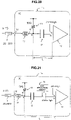
Fig. 33 shows an example of a general signal transmission/reception arrangement which includes a DC-blocking capacitor. In the example shown inFig. 33 , a transmission-side circuit 10-1 and a 50-Ω resistor 11-1 for impedance matching are arranged in a transmission-side IC 1-1, and a reception-side circuit 10-2 and a 50-Ω resistor 11-2 for impedance matching are arranged in a transmission-side IC 1-2. The IC 1-1 and the IC 1-2 are connected by a transmission line 101, and a DC-blocking capacitor 3 is arranged in the middle of the transmission line 101. - In the example shown in
Fig. 33 , since the DC-blockingcapacitor 3 and the 50-Ω resistor 11-2 on the reception-side form a high-pass filter, a low frequency component which includes the DC components of the signal is cut off (blocked). However, in the case of an application that handles a baseband signal having a wide band which ranges from several Gbps to several ten Gbps, a signal frequency component of about 1 MHz or more needs to be passed, thus creating a need to set the cutoff frequency of the high-pass filter to about 1 MHz or less. - The transfer function of a high-pass filter using a capacitor C and a resistor R as shown in
Fig. 34 is as follows.
- According to equation (1), it can be seen that, when the value of the resistor R is a fixed value of 50 Ω to ensure impedance matching, the capacitor C needs to be set to about 5 nF or more (nF order) to implement a cutoff frequency of about 1 MHz. It is difficult, in terms of the dedicated area, to manufacture an nF-order capacitor on a chip by a general semiconductor process, and a DC-blocking capacitor needs to be mounted externally (off the chip) (see non-patent literature 1).
- However, since the size of an external capacitor is several hundred µm to mm square, it problematically inhibits the downsizing of a module or the like that incorporates the external capacitor.
-
US 2013/002347 A1 discloses an integrated circuit according to the preamble ofclaim 1. - Non-Patent Literature 1: H. Wakita, et al., "36-GHz-Bandwidth Quad-channel Driver Module using Compact QFN Package for Optical Coherent Systems", Electrical Performance of Electronic Packaging and Systems (EPEPS), 2015
- The present invention has been made to solve the above-described problem and has as its object to implement a compact wideband DC-blocking circuit that can be mounted on an IC chip while ensuring impedance matching.
- An IC chip according to the present invention is set out in
independent claim 1. The dependent claims relate to preferred embodiments. - The present application discloses a IC chip comprising: a pad (15) connected to a first transmission line (2) outside the chip; a signal line (16), one end of which is connected to the pad;a termination resistor (11) connected to the other end of the signal line and configured to terminate the first transmission line;a reception-side input unit circuit (10) configured to receive a signal transmitted from a transmission-side via the first transmission line; and a capacitor (12) inserted between a node (A) of the signal line and the termination resistor and an input terminal of the reception-side input unit circuit, characterized in that a length (L) from the node of the signal line and the termination resistor to the input terminal of the reception-side input unit circuit is shorter than a wavelength of a maximum frequency component of a signal handled by the reception-side input unit circuit.
-
-
Fig. 1 is a circuit diagram showing the arrangement of a reception-side IC chip according to the first embodiment of the present invention; -
Fig. 2 is a circuit diagram showing the arrangement of a reception-side IC chip according to the second embodiment of the present invention; -
Fig. 3 is a circuit diagram showing the arrangement of a reception-side IC chip according to the third embodiment of the present invention; -
Fig. 4 is a circuit diagram showing the arrangement of a reception-side IC chip according to the fourth embodiment of the present invention; -
Fig. 5 is a circuit diagram showing the arrangement of a reception-side IC chip according to the fifth embodiment of the present invention; -
Fig. 6 is a circuit diagram showing another arrangement of the reception-side IC chip according to the fifth embodiment of the present invention; -
Fig. 7 is a circuit diagram showing the arrangement of a reception-side IC chip according to the sixth embodiment of the present invention; -
Fig. 8 is a circuit diagram showing another arrangement of the reception-side IC chip according to the sixth embodiment of the present invention; -
Fig. 9 is a circuit diagram showing the arrangement of a reception-side IC chip according to the seventh embodiment of the present invention; -
Fig. 10 is a circuit diagram showing another arrangement of the reception-side IC chip according to the seventh embodiment of the present invention; -
Fig. 11 is a circuit diagram showing the arrangement of a reception-side IC chip according to the eighth embodiment of the present invention; -
Fig. 12 is a circuit diagram showing another arrangement of the reception-side IC chip according to the eighth embodiment of the present invention; -
Figs. 13A and 13B are circuit diagrams showing examples of the arrangement of an input stage of a reception-side input unit circuit according to the first to fourth embodiments of the present invention; -
Figs. 14A and 14B are circuit diagrams showing examples of the arrangement of an input stage of a reception-side input unit circuit according to the fifth to eighth embodiments of the present invention; -
Fig. 15 is a circuit diagram showing an example of the arrangement of a bias application circuit according to the third, fourth, seventh, and eighth embodiment of the present invention; -
Fig. 16 is a circuit diagram showing the arrangement of a reception-side IC chip according to the 12th embodiment of the present invention; -
Fig. 17 is a circuit diagram showing another arrangement of the reception-side IC chip according to the 12th embodiment of the present invention; -
Fig. 18 is a circuit diagram showing the arrangement of a conventional reception-side IC chip targeting evaluation by simulation; -
Fig. 19 is a graph showing a frequency characteristic simulation results of the conventional reception-side IC chip and the reception-side IC chip of the present invention; -
Fig. 20 is a circuit diagram showing the arrangement of a reception-side IC chip according to the 13th embodiment of the present invention; -
Fig. 21 is a circuit diagram showing another arrangement of the reception-side IC chip according to the 13th embodiment of the present invention; -
Fig. 22 is a circuit diagram showing yet another arrangement of the reception-side IC chip according to the 13th embodiment of the present invention; -
Fig. 23 is a circuit diagram showing still yet another arrangement of the reception-side IC chip according to the 13th embodiment of the present invention; -
Fig. 24 is a circuit diagram showing the arrangement of a reception-side IC chip according to the 14th embodiment of the present invention; -
Fig. 25 is a circuit diagram showing another arrangement of the reception-side IC chip according to the 14th embodiment of the present invention; -
Fig. 26 is a circuit diagram showing yet another arrangement of the reception-side IC chip according to the 14th embodiment of the present invention; -
Fig. 27 is a circuit diagram showing still yet another arrangement of the reception-side IC chip according to the 14th embodiment of the present invention; -
Fig. 28 is a circuit diagram showing the arrangement of a reception-side IC chip according to the 15th embodiment of the present invention; -
Fig. 29 is a circuit diagram showing the arrangement of an electrostatic discharge protection circuit of the reception-side IC chip according to the 15th embodiment of the present invention; -
Fig. 30 is a circuit diagram showing another arrangement of the reception-side IC chip according to the 15th embodiment of the present invention; -
Fig. 31 is a circuit diagram showing yet another arrangement of the reception-side IC chip according to the 15th embodiment of the present invention; -
Fig. 32 is a circuit diagram showing still yet another arrangement of the reception-side IC chip according to the 15th embodiment of the present invention; -
Fig. 33 is a view showing an example of a connection arrangement between ICs via a DC-blocking capacitor which is used in general; and -
Fig. 34 is a view for explaining the arrangement and a transfer coefficient of a high-pass filter. - In order to solve the above-described problem, the present invention provides a compact wideband DC-blocking circuit that can be mounted on an IC chip while ensuring 50-Ω impedance matching. In the present invention, a blocking capacitor, which is conventionally arranged on a transmission line between a transmission-side IC chip and a reception-side IC chip, is arranged on the reception-side IC chip.
- Embodiments of the present invention will be described hereinafter with reference to the attached drawings.
Fig. 1 is a circuit diagram showing a reception-side IC chip according to the first embodiment of the present invention. A reception-side IC chip 1a at least includes apad 15 connected to atransmission line 2 whose characteristic impedance Z0 from outside the chip is 50 Ω, asignal line 16, one end of which is connected to thepad 15, a reception-sideinput unit circuit 10 that receives a signal S transmitted from a transmission-side IC chip (not shown) via thetransmission line 2, a 50-Ω termination resistor 11 for impedance matching that is connected between a predetermined voltage and the other end of thesignal line 16 and terminates thetransmission line 2, and acapacitor 12 inserted between a node A of thesignal line 16 and thetermination resistor 11 and an input terminal In of the reception-sideinput unit circuit 10. - In such reception-
side IC chip 1a, an on-chip DC-blocking circuit according this embodiment is formed by thecapacitor 12. - In this embodiment, an input impedance Zin of the reception-side
input unit circuit 10 needs to be increased to make thecapacitor 12 be of a size that can be mounted on a chip. The degree to which the input impedance Zin is to be set will be described later. - The Second embodiment of the present invention will be described next.
Fig. 2 is a circuit diagram showing the arrangement of a reception-side IC chip according to the second embodiment of the present invention. A reception-side IC chip 1b according to this embodiment has the same arrangement as the first embodiment, but is characterized in that a length L from a node A of asignal line 16 and atermination resistor 11 to an input terminal In of a reception-sideinput unit circuit 10 is sufficiently shorter than the wavelength of a maximum frequency component of a signal S handled by the reception-side IC chip 1b (reception-side input unit circuit 10). - For example, the length L can be set to be less than 1/20 of the wavelength of the maximum frequency component of the signal S handled by the reception-
side IC chip 1b (reception-side input unit circuit 10). In general, it is known that a circuit whose length L is of a size less than 1/20 of a signal wavelength can be handled as a lumped constant circuit. That is, as long as the size is less than 1/20 of the signal wavelength, the signal waveform will not be influenced even under a state in which a reflected wave or the like will occur. - The third embodiment of the present invention will be described next.
Fig. 3 is a circuit diagram showing the arrangement of a reception-side IC chip according to the third embodiment of the present invention. A reception-side IC chip 1c according to this embodiment is obtained by adding, to the arrangement of the first embodiment, abias application circuit 13 that applies a DC bias voltage to an input terminal In of a reception-sideinput unit circuit 10. - In this embodiment, in order to make a
capacitor 12 of an on-chip DC-blocking circuit be of a size that can be mounted on a chip, an input impedance Zin of the reception-sideinput unit circuit 10 and an output impedance Zout of thebias application circuit 13 need to be increased. The degrees to which the input impedance Zin and the output impedance Zout are to be set will be described later. - The fourth embodiment of the present invention will be described next.
Fig. 4 is a circuit diagram showing the arrangement of a reception-side IC chip according to the fourth embodiment of the present invention. A reception-side IC chip 1d according to this embodiment has the same arrangement as the third embodiment, but is characterized in that a length L from a node A of asignal line 16 and atermination resistor 11 to an input terminal In of a reception-sideinput unit circuit 10 is sufficiently shorter than the wavelength of a maximum frequency component of a signal S handled by the reception-side IC chip 1d (reception-side input unit circuit 10). In the same manner as the third embodiment, the length L can be set to be less than 1/20 of the wavelength of the maximum frequency component of the signal S handled by the reception-side IC chip 1d (reception-side input unit circuit 10). - As described above, by using a DC-blocking circuit arrangement that has the characteristics described in the first to fourth embodiments, impedance matching by the 50-
Ω termination resistor 11 arranged before acapacitor 12 can be ensured and a resistance value R, as indicated in the circuit shown inFig. 34 , can be designed to be sufficiently large when the reception-sideinput unit circuit 10 is viewed from the node A of thesignal line 16 and thetermination resistor 11. As a result, the cutoff frequency of a high-pass filter can be extended to a low frequency range even if the value of thecapacitor 12 is reduced. - For example, in the case of the first and second embodiments, a high-pass filter is formed by the
capacitor 12 and an input impedance Zin of the reception-sideinput unit circuit 10. The input impedance Zin (the value of the resistor R) can be set based on equation (1) so that the cutoff frequency of the high-pass filter and the capacitance of thecapacitor 12 become desired values, respectively. - Also, in the case of the third and fourth embodiments, a high-pass filter is formed by the
capacitor 12 and a combined resistance of the input impedance Zin of the reception-sideinput unit circuit 10 and an output impedance Zout of abias application circuit 13. The input impedance Zin and the output impedance Zout can be set so that the cutoff frequency of the high-pass filter and the capacitance of thecapacitor 12 become desired values, respectively. For example, if the combined resistance value of the input impedance Zin of the reception-sideinput unit circuit 10 and the output impedance Zout of thebias application circuit 13 is designed to be about 1M Ω, the capacitance value of thecapacitor 12 necessary to implement a cutoff frequency of 1 MHz can be 1 pF or less. That is, thecapacitor 12 will be of a size that can be mounted on a chip. - In addition, in the second and fourth embodiments, by designing the length L from the node A of the
signal line 16 and thetermination resistor 11 to the input terminal In of the reception-sideinput unit circuit 10 to be sufficiently shorter than the wavelength of the maximum frequency component of the signal S to be handled, characteristic degradation (the influence from the reflection due to impedance mismatch between the node A and the reception-side input unit circuit 10) at the high-frequency range can be suppressed. - As described above, by using the circuit arrangements according to the first to fourth embodiments, a compact wideband DC-blocking circuit which is mountable on an IC chip can be implemented while ensuring 50-Ω impedance matching.
- Although the first to fourth embodiments showed examples of application to a circuit that handles a single-phase signal S, the present invention can also be applied to a differential circuit.
Fig. 5 is a circuit diagram showing the arrangement of a reception-side IC chip according to the fifth embodiment of the present invention. A reception-side IC chip 1e at least includes a pad 15p connected to a non-inverting-side transmission line 2p whose characteristic impedance Z0 is 50 Ω, a pad 15n connected to an inverting-side transmission line 2n whose characteristic impedance z0 is 50 Ω, a signal line 16p, one end of which is connected to the pad 15p, a signal line 16n, one end of which is connected to the pad 15n, a reception-side input unit circuit 10e which receives a differential signal DS from a transmission-side IC chip (not shown) via the transmission lines 2p and 2n having a differential arrangement, a 50-Ω termination resistor 11p for impedance matching which is connected between a predetermined voltage and the other end of the signal line 16p and terminates the transmission line 2p, a 50-Ω termination resistor 11n for impedance matching which is connected between a predetermined voltage and the other end of the signal line 16n and terminates the transmission line 2n, a capacitor 12p inserted between a non-inverting input terminal Inp of the reception-side input unit circuit 10e and a node Ap of the signal line 16p and the termination resistor 11p, and a capacitor 12n inserted between an inverting input terminal Inn of the reception-side input unit circuit 10e and a node An of the signal line 16n and the termination resistor 11n. - In such reception-
side IC chip 1e, an on-chip DC-blocking circuit according to this embodiment is formed by thecapacitors - In this embodiment, to make each of the
capacitors input unit circuit 10e need to be increased. The degrees to which the input impedances Zinp and Zinn are to be set will be described later. - Note that the
termination resistors Fig. 5 , as a measure against common mode noise or may be arranged as a π-shaped termination as a reception-side IC chip 1f as shown inFig.6 . - The sixth embodiment of the present invention will be described below.
Fig. 7 is a circuit diagram showing the arrangement of a reception-side IC chip according to the sixth embodiment of the present invention. A reception-side IC chip 1g according to this embodiment has the same arrangement as the fifth embodiment, but is characterized in that a length Lp, from a node Ap of a non-inverting-side signal line 16p and atermination resistor 11p to a non-inverting input terminal Inp of a reception-sideinput unit circuit 10e, and a length Ln, from a node An of an inverting-side signal line 16n and atermination resistor 11n to an inverting input terminal Inn of the reception-sideinput unit circuit 10e will be sufficiently shorter than the wavelength of the maximum frequency component of a signal DS handled by the reception-side IC chip 1g (reception-sideinput unit circuit 10e). - In the same manner as the second embodiment, the lengths Lp and Ln can be set to be less than 1/20 of the wavelength of the maximum frequency component of the signal DS handled by the reception-
side IC chip 1g (reception-sideinput unit circuit 10e). - As described in the fifth embodiment, a T-shaped termination, as shown in
Fig. 7 , may be arranged as a measure against common mode noise or a π-shaped termination as that of a reception-side IC chip 1h shown inFig. 8 may be arranged. - The seventh embodiment of the present invention will be described next.
Fig. 9 is a circuit diagram showing the arrangement of a reception-side IC chip according to the seventh embodiment of the present invention. A reception-side IC chip 1i according to the embodiment is obtained by adding, to the arrangement of the fifth embodiment, abias application circuit 13p, which applies a DC bias voltage to a non-inverting input terminal Inp of the reception-sideinput unit circuit 10e, and abias application circuit 13n, which applies a DC bias voltage to a inverting input terminal Inn of the reception-sideinput unit circuit 10e. - In this embodiment, to make
capacitors input unit circuit 10e and output impedances Zoutp and Zoutn of thebias application circuits - As described in the fifth embodiment, a T-shaped terminal arrangement, as shown in
Fig. 9 , may be used as a measure against common mode noise or a π-shaped terminal arrangement as that of a reception-side IC chip 1j shown inFig. 10 may be used. - The eighth embodiment of the present invention will be described next.
Fig. 11 is a circuit diagram showing the arrangement of a reception-side IC chip according to the eighth embodiment of the present invention. A reception-side IC chip 1k according to the embodiment has the same arrangement as the seventh embodiment, but is characterized in that a length Lp, from a node Ap of a non-inverting-side signal line 16p and atermination resistor 11p to a non-inverting input terminal Inp of a reception-sideinput unit circuit 10e, and a length Ln, from a node An of an inverting-side signal line 16n and atermination resistor 11n to an inverting input terminal Inn of the reception-sideinput unit circuit 10e will be sufficiently shorter than the wavelength of the maximum frequency component of a differential signal DS handled by the reception-side IC chip 1k (reception-sideinput unit circuit 10e). In the same manner as the sixth embodiment, the lengths Lp and Ln can be set to be less than 1/20 of the wavelength of the maximum frequency component of the signal DS handled by the reception-side IC chip 1k (reception-sideinput unit circuit 10e). - As described in the fifth embodiment, a T-shaped termination, as shown in
Fig. 11 , may be arranged as a measure against common mode noise or a π-shaped termination as that of a reception-side IC chip 11 shown inFig. 12 may be arranged. - As described above, by using an IC chip that has the characteristics described in the fifth to eighth embodiments, the same effects as those of the first to fourth embodiments can be obtained in a differential circuit. In the case of the fifth and sixth embodiments, a high-pass filter is formed by a
capacitor 12p and a non-inverting-side input impedance Zinp of the reception-sideinput unit circuit 10e. The input impedance Zinp (the value of a resistor R) can be set based on equation (1) so that the cutoff frequency of the high-pass filter and the capacitance of thecapacitor 12p become desired values, respectively. In the same manner, since a high-pass filter is formed by acapacitor 12n and an inverting-side input impedance Zinn of the reception-sideinput unit circuit 10e, the input impedance Zinn (the value of the resistor R) can be set so that the cutoff frequency of the high-pass filter and the capacitance of thecapacitor 12n become desired values, respectively. - Also, in the case of the seventh and eighth embodiments, a high-pass filter is formed by the
capacitor 12p and a combined resistance of the non-inverting-side input impedance Zinp of the reception-sideinput unit circuit 10e and an output impedance Zoutp of abias application circuit 13p. The input impedance Zinp and the output impedance Zoutp can be set so that the cutoff frequency of the high-pass filter and the capacitance of thecapacitor 12p become desired values, respectively. In the same manner, since a high-pass filter is formed by thecapacitor 12n and a combined resistance of the inverting-side input impedance Zinn of the reception-sideinput unit circuit 10e and an output impedance Zoutn of abias application circuit 13n, the input impedance Zinn and the output impedance Zoutn can be set so that the cutoff frequency of the high-pass filter and the capacitance of thecapacitor 12n become desired values, respectively. - An example of the arrangement of a reception-side
input unit circuit 10 according to each of the first to fourth embodiments will be described next. As described above, the reception-sideinput unit circuit 10 that has a high input impedance needs to be arranged to implement the IC chip according to each of the first to fourth embodiments. As the circuit arrangement, a circuit which uses the base as an input is suitable in a case in which a bipolar transistor is to be used, and a circuit which uses the gate as an input is suitable in a case in which an FET (field effect transistor) is to be used. - That is, in the case of a bipolar transistor, it is preferable to use an emitter follower formed by a bipolar transistor Q1 and a current source IS1, as shown in
Fig. 13A , as the arrangement of an input stage of the reception-sideinput unit circuit 10. Also, in the case of an FET, it is preferable to use a source follower formed by an FET Q2 and a current source IS2, as shown inFig. 13B , as the arrangement of the input stage of the reception-sideinput unit circuit 10. - An example of the arrangement of a reception-side
input unit circuit 10e according to each of the fifth to eighth embodiments will be described next. In the same manner as the first to fourth embodiments, the reception-sideinput unit circuit 10e that has a high input impedance needs to be arranged to implement the IC chip according to each of the fifth to eighth embodiments. - In the case of a bipolar transistor, it is preferable to use, as the arrangement of an input stage of the reception-side
input unit circuit 10e, a differential circuit formed by bipolar transistors Q3 and Q4, resistors R1 and R2, and a current source IS3 as shown inFig. 14A . Also, in the case of an FET, it is preferable to use, as the arrangement of the input stage of the reception-sideinput unit circuit 10e, a differential circuit formed by FETs Q5 and Q6, resistors R3 and R4, and a current source IS4 as shown inFig. 14B . - An example of the arrangement of
bias application circuits bias application circuit 13 according to the third and fourth embodiments can be implemented by a voltage divider circuit that is formed, for example, as shown inFig. 15 , by a resistor R5 in which one terminal is connected to a positive power supply voltage VCC (VDD in a case in which a reception-sideinput unit circuit 10 is formed by an FET) and the other terminal is connected to an output terminal of thebias application circuit 13, and a resistor R6 in which one terminal is connected to the output terminal of thebias application circuit 13 and the other terminal is connected to a negative power supply voltage VEE (VSS in the case in which the reception-sideinput unit circuit 10 is formed by an FET). - The
bias application circuits - As described above, to make
capacitors bias application circuits bias application circuit - The 12th embodiment of the present invention will be described next.
Fig. 16 is a circuit diagram showing the arrangement of a reception-side IC chip according to the 12th embodiment of the present invention. A reception-side IC chip 1m according to this embodiment is characterized in that atransmission line 14 having a characteristic impedance z0 of 50 Ω or more has been inserted in series to asignal line 16 of the arrangement according to the first embodiment or the second embodiment. - In this embodiment, the insertion of the
transmission line 14 can suppress, in an input unit of the reception-side IC chip 1m, the influence of a parasitic capacitance from an input port (a signal input pad connected to atransmission line 2 or the like) to atermination resistor 11. - The
transmission line 14 can be applied to any of the first to eighth embodiments. If it is to be applied to the fifth to eighth embodiments,transmission lines lines Fig. 17 . Although the arrangement ofFig. 17 shows a case in which thetransmission lines Fig. 5 , they can also be applied to each ofFigs. 6 to 12 in the same manner. - Finally, the effects of the present invention will be described hereinafter. To confirm the effects of the present invention, a case in which a capacitor of 2.5 pF having a size that can be mounted on a chip is used in a conventional arrangement and a case in which the capacitor is used in the arrangement of the present invention are compared by a circuit simulator by using an example of a wideband amplifier.
- As shown in
Fig. 18 , the conventional arrangement uses an arrangement in which acapacitor 120 of 2.5 pF is inserted between the terminal of thetransmission line 2 and a node of thetermination resistor 11 and an input terminal of a reception-sideinput unit circuit 10. - On the other hand, the arrangement of the present invention uses an arrangement in which the capacitance of a
capacitor 12 in a reception-side IC chip 1d according to the fourth embodiment shown inFig. 4 is 2.5 pF. -
Fig. 19 is a graph showing a frequency characteristic simulation results of the conventional reception-side IC chip and the reception-side IC chip of the present invention. InFig. 19 ,reference numeral 180 indicates the frequency characteristic of the conventional reception-side IC chip, andreference numeral 181 indicates the frequency characteristic of the reception-side IC chip of the present invention. - It can be seen in
Fig. 19 that using the arrangement of the present invention allows the cutoff frequency of a low frequency range to be extended from 600 MHz to 20 kHz without degrading high frequency characteristics. As described above, the present invention can be used to implement a compact wideband DC-blocking circuit that can be mounted on an IC chip. - The 13th embodiment of the present invention will be described next.
Fig. 20 is a circuit diagram showing the arrangement of a reception-side IC chip according to the 13th embodiment of the present invention. A reception-side IC chip 1n according to this embodiment is characterized in that aninductor 17 is inserted in series to asignal line 16 in the arrangement of the first embodiment or the second embodiment. - In the first to 12th embodiments, degradation of the reflection characteristics/impedance matching on the high-frequency side occurs because a parasitic capacitance due to circuit layout is added to nodes A, Ap, and An of
termination resistors capacitors inductor 17 can be inserted as shown inFig. 20 to suppress the degradation of the reflection characteristic. In this case, since theinductor 17 has an inductance value of a small pH order, it can be regarded to be short-circuited in the low frequency range. Hence, theinductor 17 will not greatly influence the cutoff frequency of the low frequency range that needs to be ensured in the present invention. -
Fig. 21 shows the arrangement of a reception-side IC chip 1o obtained in a case in which theinductor 17 is applied toFig. 3 according to the third embodiment orFig. 4 according to the fourth embodiment. -
Fig. 22 shows the arrangement of a reception-side IC chip 1p obtained in a case in whichinductors lines Fig. 5 according to the fifth embodiment. Although the arrangement ofFig. 22 shows a case in which theinductors Fig. 5 , the arrangement can be applied in the same manner to each ofFigs. 6 to 8 . -
Fig. 23 shows the arrangement of a reception-side IC chip 1q obtained in a case in which theinductors signal lines Fig. 9 according to the seventh embodiment. Although the arrangement ofFig. 23 shows a case in which theinductors Fig. 9 , the arrangement can be applied in the same manner to each ofFigs. 10 to 12 . - The 14th embodiment of the present invention will be described next.
Fig. 24 is a circuit diagram showing the arrangement of a reception-side IC chip according to the 14th embodiment of the present invention. A reception-side IC chip 1r according to this embodiment is characterized in that aninductor 18 is inserted in series to asignal line 16 between apad 15 and atransmission line 14 and aninductor 19 is inserted in series to thesignal line 16 between thetransmission line 14 and a node A of thesignal line 16 and atermination resistor 11 in the arrangement according to the 12th embodiment. - As a result, the degradation of the reflection characteristic in the high-frequency range due to parasitic capacitance of the
pad 15 can be suppressed in this embodiment. -
Fig. 25 shows the arrangement of a reception-side IC chip 1s obtained in a case in which theinductors Fig. 3 according to the third embodiment orFig. 4 according to the fourth embodiment. -
Fig. 26 shows the arrangement of a reception-side IC chip 1t obtained in a case in whichinductors inductors lines Fig. 17 according to the 12th embodiment. Although the arrangement ofFig. 26 shows a case in which theinductors Fig. 17 , the arrangement can be applied in the same manner to an arrangement obtained by serially insertingtransmission lines signal lines Figs. 6 to 8 . -
Fig. 27 shows the arrangement of a reception-side IC chip 1u obtained in a case in which thetransmission lines signal lines inductors inductors signal lines Fig. 9 according to the seventh embodiment. Although the arrangement ofFig. 27 shows a case in which theinductors Fig. 9 , the arrangement can be applied in the same manner to an arrangement obtained by serially inserting thetransmission lines signal lines Figs. 10 to 12 . - The 15th embodiment of the present invention will be described next.
Fig. 28 is a circuit diagram showing the arrangement of a reception-side IC chip according to the 15th embodiment of the present invention. A reception-side IC chip 1v according to this embodiment is characterized in that atransmission line 14 is formed by two transmission lines 14-1 and 14-2, which are connected in series, and an ESD (ElectroStatic Discharge)protection circuit 20, which is connected to asignal line 16 between the two transmission lines 14-1 and 14-2, are included in the arrangement according to the 14th embodiment shown inFig. 24 . - For example, when the IC is to be handled at the time of an implementation process, there is a possibility that the resistor, the capacitor, or the transistor of a reception-side input unit circuit will be damaged due to ESD. The
ESD protection circuit 20 is arranged in the IC chip to improve ESD resistance. However, to suppress the influence (such as the reflection characteristic degradation or the like) of parasitic capacitance due to the addition of theESD protection circuit 20, the two transmission lines 14-1 and 14-2 having a characteristic impedance Z0 of 50 Ω or more are arranged, and theESD protection circuit 20 is arranged at the node of these two transmission lines 14-1 and 14-2. -
Fig. 29 shows the arrangement of theESD protection circuit 20. TheESD protection circuit 20 is formed by N diodes D1, which are connected to set a reverse bias state between a positive power supply voltage VCC (VDD in a case in which a reception-sideinput unit circuit 10 is formed by an FET) and thesignal line 16, and M diodes D2, which are connected to set a reverse bias state between a negative power supply voltage VEE (VSS in a case in which the reception-sideinput unit circuit 10 is formed by an FET) and thesignal line 16. - The stage counts N and M of the diodes D1 and D2, respectively, are parameters that are set arbitrarily to fall within a range in which the diodes D1 and D2 will not break down in accordance with the voltage (a DC operating point in an operation state) of the
signal line 16. That is, N ≥ 0 and M ≥ 0. - In this manner, this embodiment can implement a compact and wideband DC-blocking circuit with high ESD resistance that can be mounted on an IC chip.
-
Fig. 30 shows the arrangement of a reception-side IC chip 1w obtained in a case in which thetransmission line 14 is formed by the two transmission lines 14-1 and 14-2 which are connected in series and an ESD (Electrostatic Discharge)protection circuit 20 is connected to thesignal line 16 between the two transmission lines 14-1 and 14-2 in the arrangement shown inFig. 25 according to the 14th embodiment. -
Fig. 31 shows the arrangement of a reception-side IC chip 1x obtained in a case in which atransmission line 14p is formed by twotransmission lines 14p-1 and 14p-2 having the characteristic impedance Z0 of 50 Ω or more, atransmission line 14n is formed by twotransmission lines 14n-1 and 14n-2 having the characteristic impedance Z0 of 50 Ω or more, anESD protection circuit 20p is connected to asignal line 16p between the twotransmission lines 14p-1 and 14p-2 which are connected in series, and anESD protection circuit 20n is connected to asignal line 16n between the twotransmission lines 14n-1 and 14n-2 which are connected in series in the arrangement shown inFig. 26 according to the 14th embodiment. The arrangement of each of theESD protection circuits ESD protection circuit 20. Although the arrangement ofFig. 31 shows a case in which theESD protection circuits Fig. 26 , the arrangement can be applied in the same manner to an arrangement obtained by serially inserting thetransmission lines 14p-1 and 14p-2 andinductors signal line 16p and serially inserting thetransmission lines 14n-1 and 14n-2 andinductors signal line 16n in each ofFigs. 6 to 8 . -
Fig. 32 shows the arrangement of a reception-side IC chip 1y obtained in a case in which thetransmission line 14p is formed by the twotransmission lines 14p-1 and 14p-2 having the characteristic impedance Z0 of 50 Ω or more, thetransmission line 14n is formed by twotransmission lines 14n-1 and 14n-2 having the characteristic impedance Z0 of 50 Ω or more, theESD protection circuit 20p is connected to thesignal line 16p between the twotransmission lines 14p-1 and 14p-2 which are connected in series, and theESD protection circuit 20n is connected to thesignal line 16n between the twotransmission lines 14n-1 and 14n-2 which are connected in series in the arrangement shown inFig. 27 according to the 14th embodiment. Although the arrangement ofFig. 32 shows a case in which theESD protection circuits Fig. 27 , the arrangement can be applied in the same manner to an arrangement obtained by serially inserting thetransmission lines 14p-1 and 14p-2 and theinductors signal line 16p and serially inserting thetransmission lines 14n-1 and 14n-2 and theinductors signal line 16n in each ofFigs. 10 to 12 . - The present invention can be applied to an IC chip that performs high-speed electrical signal communication.
- 1a-1y...reception-side IC chip, 2, 2p, 2n, 14, 14-1, 14-2, 14p, 14p-1, 14p-2, 14n, 14n-1, 14n-2...transmission line, 10, 10e...reception-side input unit circuit, 11, 11p, 11n...termination resistor, 12, 12p, 12n...capacitor, 13, 13p, 13n...bias application circuit, 15, 15p, 15n...pad, 16, 16p, 16n...signal line, 17, 17p, 17n, 18, 18p, 18n, 19, 19p, 19n...inductor, 20, 20p, 20n...ESD protection circuit, Q1, Q3, Q4...bipolar transistor, Q2, Q5, Q6...FET, IS1 - IS4...current source, R1 - R6...resistor, D1, D2...diode.
Claims (10)
- An IC chip comprising:a pad (15) connected to a first transmission line (2) outside the chip;a signal line (16), one end of which is connected to the pad;a termination resistor (11) connected to the other end of the signal line and configured to terminate the first transmission line;a reception-side input unit circuit (10) configured to receive a signal transmitted from a transmission-side via the first transmission line; anda capacitor (12) inserted between a node (A) of the signal line and the termination resistor and an input terminal of the reception-side input unit circuit,characterized in that a length (L) from the node of the signal line and the termination resistor to the input terminal of the reception-side input unit circuit is shorter than a wavelength of a maximum frequency component of a signal handled by the reception-side input unit circuit.
- The IC chip according to claim 1, wherein the capacitor and an input impedance of the reception-side input unit circuit form a high-pass filter.
- The IC chip according to claim 1, further comprising:
a bias application circuit (13) configured to apply a DC bias voltage to the input terminal of the reception-side input unit circuit. - The IC chip according to claim 3, wherein a high-pass filter is formed by the capacitor and a combined resistance of an input impedance of the reception-side input unit circuit and an output impedance of the bias application circuit.
- The IC chip according to claim 4, wherein a resistance value of the termination resistor is 50 Ω,a combined resistance value of the input impedance of the reception-side input unit circuit and the output impedance of the bias application circuit is 1 MΩ, anda capacitance value of the capacitor is 1 pF or less.
- The IC chip according to claim 4, whereina resistance value of the termination resistor is 50 Ω, andthe input impedance of the reception-side input unit circuit and the output impedance of the bias application circuit are set so that a cutoff frequency of the high-pass filter and a capacitance of the capacitor become 20 kHz and 2.5 pF, respectively.
- The IC chip according to any one of claims 1 to 4, further comprising:
an inductor (17) inserted in series to the signal line. - The IC chip according to any one of claims 1 to 4, further comprising:
a second transmission line (14) inserted in series to the signal line, the second transmission line having a characteristic impedance of not less than 50 Ω. - The IC chip according to claim 8, further comprising:a first inductor (18) inserted in series to the signal line between the pad and the second transmission line; anda second inductor (19) inserted in series to the signal line between the second transmission line and the node of the signal line and the termination resistor.
- The IC chip according to claim 9, wherein the second transmission line includes two transmission lines (14-1, 14-2) which are connected in series, and
the IC chip further comprises an electrostatic discharge protection circuit (20) which is connected to a signal line between the two transmission lines.
Applications Claiming Priority (2)
| Application Number | Priority Date | Filing Date | Title |
|---|---|---|---|
| JP2017241532 | 2017-12-18 | ||
| PCT/JP2018/045860 WO2019124211A1 (en) | 2017-12-18 | 2018-12-13 | Ic chip |
Publications (3)
| Publication Number | Publication Date |
|---|---|
| EP3731422A1 EP3731422A1 (en) | 2020-10-28 |
| EP3731422A4 EP3731422A4 (en) | 2021-09-22 |
| EP3731422B1 true EP3731422B1 (en) | 2022-11-30 |
Family
ID=66994795
Family Applications (1)
| Application Number | Title | Priority Date | Filing Date |
|---|---|---|---|
| EP18892943.4A Active EP3731422B1 (en) | 2017-12-18 | 2018-12-13 | Ic chip |
Country Status (5)
| Country | Link |
|---|---|
| US (1) | US11233393B2 (en) |
| EP (1) | EP3731422B1 (en) |
| JP (1) | JP7046981B2 (en) |
| CN (1) | CN111492591B (en) |
| WO (1) | WO2019124211A1 (en) |
Families Citing this family (1)
| Publication number | Priority date | Publication date | Assignee | Title |
|---|---|---|---|---|
| EP4187599A1 (en) * | 2021-11-25 | 2023-05-31 | Nexperia B.V. | Esd protection device |
Family Cites Families (15)
| Publication number | Priority date | Publication date | Assignee | Title |
|---|---|---|---|---|
| US4849981A (en) * | 1987-10-05 | 1989-07-18 | General Electric Company | High frequency signal driver for a laser diode and method of forming same |
| JPH09200077A (en) | 1996-01-16 | 1997-07-31 | Murata Mfg Co Ltd | Composite high frequency component |
| JP2004023547A (en) * | 2002-06-18 | 2004-01-22 | Toyota Industries Corp | Low frequency attenuating circuit and radio receiver |
| US7719380B2 (en) * | 2004-08-17 | 2010-05-18 | Hewlett-Packard Development Company, L.P. | AC coupling circuit |
| EP2040376B1 (en) * | 2006-06-13 | 2013-08-14 | Kyocera Corporation | Variable capacitance circuit |
| JP2008085987A (en) | 2006-08-30 | 2008-04-10 | Sanyo Electric Co Ltd | Impedance matching method, method of manufacturing signal processing circuit using the same, signal processing circuit, and wireless apparatus |
| JP5159776B2 (en) * | 2007-05-30 | 2013-03-13 | 京セラ株式会社 | Capacitor, resonator, filter device, communication device, and electric circuit |
| CN101527693A (en) * | 2008-03-05 | 2009-09-09 | 中兴通讯股份有限公司 | Device and method for impedance matching and bias compensation for difference transmission lines |
| JP2010028695A (en) | 2008-07-24 | 2010-02-04 | Murata Mfg Co Ltd | Noise filter component and coil component |
| JP2011009853A (en) * | 2009-06-23 | 2011-01-13 | Renesas Electronics Corp | Signal transmitter |
| CN101807884A (en) | 2010-04-28 | 2010-08-18 | 复旦大学 | Feed-forward noise cancellation resistance negative feedback broadband low noise amplifier |
| US8295018B2 (en) * | 2010-07-26 | 2012-10-23 | Taiwan Semiconductor Manufacturing Co., Ltd. | Transmission-line-based ESD protection |
| US8599966B2 (en) | 2011-06-30 | 2013-12-03 | International Business Machines Corporation | Coupling system for data receivers |
| CN103944527B (en) * | 2014-04-15 | 2017-03-08 | 华为技术有限公司 | A kind of circuit of high pass filter and integrated circuit |
| JP6609937B2 (en) * | 2015-02-27 | 2019-11-27 | 沖電気工業株式会社 | Photoelectric conversion circuit |
-
2018
- 2018-12-13 JP JP2019561017A patent/JP7046981B2/en active Active
- 2018-12-13 EP EP18892943.4A patent/EP3731422B1/en active Active
- 2018-12-13 CN CN201880081294.1A patent/CN111492591B/en active Active
- 2018-12-13 US US16/769,201 patent/US11233393B2/en active Active
- 2018-12-13 WO PCT/JP2018/045860 patent/WO2019124211A1/en unknown
Also Published As
| Publication number | Publication date |
|---|---|
| WO2019124211A1 (en) | 2019-06-27 |
| CN111492591B (en) | 2022-05-17 |
| US20210175706A1 (en) | 2021-06-10 |
| EP3731422A4 (en) | 2021-09-22 |
| CN111492591A (en) | 2020-08-04 |
| JP7046981B2 (en) | 2022-04-04 |
| US11233393B2 (en) | 2022-01-25 |
| JPWO2019124211A1 (en) | 2020-04-02 |
| EP3731422A1 (en) | 2020-10-28 |
Similar Documents
| Publication | Publication Date | Title |
|---|---|---|
| KR101486069B1 (en) | Input termination circuit and input termination device | |
| US9467106B2 (en) | Wideband bias circuits and methods | |
| EP1748551A2 (en) | Current-controlled CMOS (C3MOS) wideband input data amplifier for reduced differential and common-mode reflection | |
| US7768348B2 (en) | High-frequency circuit | |
| US9276400B2 (en) | Protection circuit | |
| EP2624448A1 (en) | Low-noise amplifier | |
| US20090231043A1 (en) | Distributed amplifier and integrated circuit | |
| US7378920B2 (en) | Methods and apparatus for a high-frequency output match circuit | |
| EP3731422B1 (en) | Ic chip | |
| US6731174B2 (en) | Radio frequency power amplifier device | |
| EP2903157A1 (en) | Microwave amplifier device | |
| US20150111514A1 (en) | High performance, low cost receiver front end | |
| EP3200343B1 (en) | Power amplifier system and associated bias circuit | |
| US9748907B2 (en) | Output impedance-matching network having harmonic-prevention circuitry | |
| JP6515493B2 (en) | Method and circuit for improving bandwidth of amplifier circuit | |
| US11323080B2 (en) | Amplification circuit, radio-frequency front end circuit, and communication device | |
| US9543902B2 (en) | Power amplifier | |
| EP3016281A1 (en) | Semiconductor amplifier bias circuit and semiconductor amplifier device | |
| JP2020109908A (en) | High frequency amplifier circuit and semiconductor device | |
| Sahu et al. | Design of low power UWB LNA for frequency 3.1–5 GHz in 0.18 μm CMOS technology | |
| US10715087B2 (en) | CMOS wideband RF amplifier with gain roll-off compensation for external parasitics | |
| Sakalas et al. | Design Approach for a Broadband Class-D Power Amplifier for Low Power Application in a 28 nm Digital CMOS Technology | |
| EP3142252B1 (en) | Video bandwidth in rf amplifiers | |
| WO2020172848A1 (en) | Travelling-wave amplifier and information transceiving device | |
| CN114598276A (en) | Multi-octave broadband power amplifier |
Legal Events
| Date | Code | Title | Description |
|---|---|---|---|
| STAA | Information on the status of an ep patent application or granted ep patent |
Free format text: STATUS: THE INTERNATIONAL PUBLICATION HAS BEEN MADE |
|
| PUAI | Public reference made under article 153(3) epc to a published international application that has entered the european phase |
Free format text: ORIGINAL CODE: 0009012 |
|
| STAA | Information on the status of an ep patent application or granted ep patent |
Free format text: STATUS: REQUEST FOR EXAMINATION WAS MADE |
|
| 17P | Request for examination filed |
Effective date: 20200609 |
|
| AK | Designated contracting states |
Kind code of ref document: A1 Designated state(s): AL AT BE BG CH CY CZ DE DK EE ES FI FR GB GR HR HU IE IS IT LI LT LU LV MC MK MT NL NO PL PT RO RS SE SI SK SM TR |
|
| AX | Request for extension of the european patent |
Extension state: BA ME |
|
| DAV | Request for validation of the european patent (deleted) | ||
| DAX | Request for extension of the european patent (deleted) | ||
| A4 | Supplementary search report drawn up and despatched |
Effective date: 20210819 |
|
| RIC1 | Information provided on ipc code assigned before grant |
Ipc: H04B 1/00 20060101ALI20210813BHEP Ipc: H03H 7/06 20060101ALI20210813BHEP Ipc: H04B 3/02 20060101AFI20210813BHEP |
|
| GRAP | Despatch of communication of intention to grant a patent |
Free format text: ORIGINAL CODE: EPIDOSNIGR1 |
|
| STAA | Information on the status of an ep patent application or granted ep patent |
Free format text: STATUS: GRANT OF PATENT IS INTENDED |
|
| INTG | Intention to grant announced |
Effective date: 20220622 |
|
| RIN1 | Information on inventor provided before grant (corrected) |
Inventor name: NAKANO, SHINSUKE Inventor name: NOSAKA, HIDEYUKI Inventor name: NAGATANI, MUNEHIKO |
|
| GRAS | Grant fee paid |
Free format text: ORIGINAL CODE: EPIDOSNIGR3 |
|
| GRAA | (expected) grant |
Free format text: ORIGINAL CODE: 0009210 |
|
| STAA | Information on the status of an ep patent application or granted ep patent |
Free format text: STATUS: THE PATENT HAS BEEN GRANTED |
|
| AK | Designated contracting states |
Kind code of ref document: B1 Designated state(s): AL AT BE BG CH CY CZ DE DK EE ES FI FR GB GR HR HU IE IS IT LI LT LU LV MC MK MT NL NO PL PT RO RS SE SI SK SM TR |
|
| REG | Reference to a national code |
Ref country code: CH Ref legal event code: EP Ref country code: GB Ref legal event code: FG4D |
|
| REG | Reference to a national code |
Ref country code: AT Ref legal event code: REF Ref document number: 1535490 Country of ref document: AT Kind code of ref document: T Effective date: 20221215 |
|
| REG | Reference to a national code |
Ref country code: IE Ref legal event code: FG4D |
|
| REG | Reference to a national code |
Ref country code: DE Ref legal event code: R096 Ref document number: 602018043833 Country of ref document: DE |
|
| REG | Reference to a national code |
Ref country code: LT Ref legal event code: MG9D |
|
| REG | Reference to a national code |
Ref country code: NL Ref legal event code: MP Effective date: 20221130 |
|
| PG25 | Lapsed in a contracting state [announced via postgrant information from national office to epo] |
Ref country code: SE Free format text: LAPSE BECAUSE OF FAILURE TO SUBMIT A TRANSLATION OF THE DESCRIPTION OR TO PAY THE FEE WITHIN THE PRESCRIBED TIME-LIMIT Effective date: 20221130 Ref country code: PT Free format text: LAPSE BECAUSE OF FAILURE TO SUBMIT A TRANSLATION OF THE DESCRIPTION OR TO PAY THE FEE WITHIN THE PRESCRIBED TIME-LIMIT Effective date: 20230331 Ref country code: NO Free format text: LAPSE BECAUSE OF FAILURE TO SUBMIT A TRANSLATION OF THE DESCRIPTION OR TO PAY THE FEE WITHIN THE PRESCRIBED TIME-LIMIT Effective date: 20230228 Ref country code: LT Free format text: LAPSE BECAUSE OF FAILURE TO SUBMIT A TRANSLATION OF THE DESCRIPTION OR TO PAY THE FEE WITHIN THE PRESCRIBED TIME-LIMIT Effective date: 20221130 Ref country code: FI Free format text: LAPSE BECAUSE OF FAILURE TO SUBMIT A TRANSLATION OF THE DESCRIPTION OR TO PAY THE FEE WITHIN THE PRESCRIBED TIME-LIMIT Effective date: 20221130 Ref country code: ES Free format text: LAPSE BECAUSE OF FAILURE TO SUBMIT A TRANSLATION OF THE DESCRIPTION OR TO PAY THE FEE WITHIN THE PRESCRIBED TIME-LIMIT Effective date: 20221130 |
|
| REG | Reference to a national code |
Ref country code: AT Ref legal event code: MK05 Ref document number: 1535490 Country of ref document: AT Kind code of ref document: T Effective date: 20221130 |
|
| PG25 | Lapsed in a contracting state [announced via postgrant information from national office to epo] |
Ref country code: RS Free format text: LAPSE BECAUSE OF FAILURE TO SUBMIT A TRANSLATION OF THE DESCRIPTION OR TO PAY THE FEE WITHIN THE PRESCRIBED TIME-LIMIT Effective date: 20221130 Ref country code: PL Free format text: LAPSE BECAUSE OF FAILURE TO SUBMIT A TRANSLATION OF THE DESCRIPTION OR TO PAY THE FEE WITHIN THE PRESCRIBED TIME-LIMIT Effective date: 20221130 Ref country code: LV Free format text: LAPSE BECAUSE OF FAILURE TO SUBMIT A TRANSLATION OF THE DESCRIPTION OR TO PAY THE FEE WITHIN THE PRESCRIBED TIME-LIMIT Effective date: 20221130 Ref country code: IS Free format text: LAPSE BECAUSE OF FAILURE TO SUBMIT A TRANSLATION OF THE DESCRIPTION OR TO PAY THE FEE WITHIN THE PRESCRIBED TIME-LIMIT Effective date: 20230330 Ref country code: HR Free format text: LAPSE BECAUSE OF FAILURE TO SUBMIT A TRANSLATION OF THE DESCRIPTION OR TO PAY THE FEE WITHIN THE PRESCRIBED TIME-LIMIT Effective date: 20221130 Ref country code: GR Free format text: LAPSE BECAUSE OF FAILURE TO SUBMIT A TRANSLATION OF THE DESCRIPTION OR TO PAY THE FEE WITHIN THE PRESCRIBED TIME-LIMIT Effective date: 20230301 |
|
| PG25 | Lapsed in a contracting state [announced via postgrant information from national office to epo] |
Ref country code: NL Free format text: LAPSE BECAUSE OF FAILURE TO SUBMIT A TRANSLATION OF THE DESCRIPTION OR TO PAY THE FEE WITHIN THE PRESCRIBED TIME-LIMIT Effective date: 20221130 |
|
| PG25 | Lapsed in a contracting state [announced via postgrant information from national office to epo] |
Ref country code: SM Free format text: LAPSE BECAUSE OF FAILURE TO SUBMIT A TRANSLATION OF THE DESCRIPTION OR TO PAY THE FEE WITHIN THE PRESCRIBED TIME-LIMIT Effective date: 20221130 Ref country code: RO Free format text: LAPSE BECAUSE OF FAILURE TO SUBMIT A TRANSLATION OF THE DESCRIPTION OR TO PAY THE FEE WITHIN THE PRESCRIBED TIME-LIMIT Effective date: 20221130 Ref country code: EE Free format text: LAPSE BECAUSE OF FAILURE TO SUBMIT A TRANSLATION OF THE DESCRIPTION OR TO PAY THE FEE WITHIN THE PRESCRIBED TIME-LIMIT Effective date: 20221130 Ref country code: DK Free format text: LAPSE BECAUSE OF FAILURE TO SUBMIT A TRANSLATION OF THE DESCRIPTION OR TO PAY THE FEE WITHIN THE PRESCRIBED TIME-LIMIT Effective date: 20221130 Ref country code: CZ Free format text: LAPSE BECAUSE OF FAILURE TO SUBMIT A TRANSLATION OF THE DESCRIPTION OR TO PAY THE FEE WITHIN THE PRESCRIBED TIME-LIMIT Effective date: 20221130 Ref country code: AT Free format text: LAPSE BECAUSE OF FAILURE TO SUBMIT A TRANSLATION OF THE DESCRIPTION OR TO PAY THE FEE WITHIN THE PRESCRIBED TIME-LIMIT Effective date: 20221130 |
|
| REG | Reference to a national code |
Ref country code: CH Ref legal event code: PL |
|
| REG | Reference to a national code |
Ref country code: BE Ref legal event code: MM Effective date: 20221231 |
|
| PG25 | Lapsed in a contracting state [announced via postgrant information from national office to epo] |
Ref country code: SK Free format text: LAPSE BECAUSE OF FAILURE TO SUBMIT A TRANSLATION OF THE DESCRIPTION OR TO PAY THE FEE WITHIN THE PRESCRIBED TIME-LIMIT Effective date: 20221130 Ref country code: LU Free format text: LAPSE BECAUSE OF NON-PAYMENT OF DUE FEES Effective date: 20221213 Ref country code: AL Free format text: LAPSE BECAUSE OF FAILURE TO SUBMIT A TRANSLATION OF THE DESCRIPTION OR TO PAY THE FEE WITHIN THE PRESCRIBED TIME-LIMIT Effective date: 20221130 |
|
| REG | Reference to a national code |
Ref country code: DE Ref legal event code: R097 Ref document number: 602018043833 Country of ref document: DE |
|
| PLBE | No opposition filed within time limit |
Free format text: ORIGINAL CODE: 0009261 |
|
| STAA | Information on the status of an ep patent application or granted ep patent |
Free format text: STATUS: NO OPPOSITION FILED WITHIN TIME LIMIT |
|
| PG25 | Lapsed in a contracting state [announced via postgrant information from national office to epo] |
Ref country code: LI Free format text: LAPSE BECAUSE OF NON-PAYMENT OF DUE FEES Effective date: 20221231 Ref country code: IE Free format text: LAPSE BECAUSE OF NON-PAYMENT OF DUE FEES Effective date: 20221213 Ref country code: CH Free format text: LAPSE BECAUSE OF NON-PAYMENT OF DUE FEES Effective date: 20221231 |
|
| 26N | No opposition filed |
Effective date: 20230831 |
|
| PG25 | Lapsed in a contracting state [announced via postgrant information from national office to epo] |
Ref country code: SI Free format text: LAPSE BECAUSE OF FAILURE TO SUBMIT A TRANSLATION OF THE DESCRIPTION OR TO PAY THE FEE WITHIN THE PRESCRIBED TIME-LIMIT Effective date: 20221130 Ref country code: BE Free format text: LAPSE BECAUSE OF NON-PAYMENT OF DUE FEES Effective date: 20221231 |
|
| PGFP | Annual fee paid to national office [announced via postgrant information from national office to epo] |
Ref country code: GB Payment date: 20231220 Year of fee payment: 6 |
|
| PGFP | Annual fee paid to national office [announced via postgrant information from national office to epo] |
Ref country code: FR Payment date: 20231222 Year of fee payment: 6 Ref country code: DE Payment date: 20231214 Year of fee payment: 6 |