EP3731149A1 - Magnetic marker and magnetic marker system - Google Patents
Magnetic marker and magnetic marker system Download PDFInfo
- Publication number
- EP3731149A1 EP3731149A1 EP18893066.3A EP18893066A EP3731149A1 EP 3731149 A1 EP3731149 A1 EP 3731149A1 EP 18893066 A EP18893066 A EP 18893066A EP 3731149 A1 EP3731149 A1 EP 3731149A1
- Authority
- EP
- European Patent Office
- Prior art keywords
- magnetic marker
- antenna
- magnetic
- conductive layer
- main body
- Prior art date
- Legal status (The legal status is an assumption and is not a legal conclusion. Google has not performed a legal analysis and makes no representation as to the accuracy of the status listed.)
- Pending
Links
Images





Classifications
-
- G—PHYSICS
- G06—COMPUTING OR CALCULATING; COUNTING
- G06K—GRAPHICAL DATA READING; PRESENTATION OF DATA; RECORD CARRIERS; HANDLING RECORD CARRIERS
- G06K19/00—Record carriers for use with machines and with at least a part designed to carry digital markings
- G06K19/06—Record carriers for use with machines and with at least a part designed to carry digital markings characterised by the kind of the digital marking, e.g. shape, nature, code
- G06K19/067—Record carriers with conductive marks, printed circuits or semiconductor circuit elements, e.g. credit or identity cards also with resonating or responding marks without active components
- G06K19/07—Record carriers with conductive marks, printed circuits or semiconductor circuit elements, e.g. credit or identity cards also with resonating or responding marks without active components with integrated circuit chips
- G06K19/077—Constructional details, e.g. mounting of circuits in the carrier
- G06K19/07749—Constructional details, e.g. mounting of circuits in the carrier the record carrier being capable of non-contact communication, e.g. constructional details of the antenna of a non-contact smart card
- G06K19/07773—Antenna details
-
- G—PHYSICS
- G06—COMPUTING OR CALCULATING; COUNTING
- G06K—GRAPHICAL DATA READING; PRESENTATION OF DATA; RECORD CARRIERS; HANDLING RECORD CARRIERS
- G06K19/00—Record carriers for use with machines and with at least a part designed to carry digital markings
- G06K19/06—Record carriers for use with machines and with at least a part designed to carry digital markings characterised by the kind of the digital marking, e.g. shape, nature, code
- G06K19/067—Record carriers with conductive marks, printed circuits or semiconductor circuit elements, e.g. credit or identity cards also with resonating or responding marks without active components
- G06K19/07—Record carriers with conductive marks, printed circuits or semiconductor circuit elements, e.g. credit or identity cards also with resonating or responding marks without active components with integrated circuit chips
- G06K19/077—Constructional details, e.g. mounting of circuits in the carrier
- G06K19/07749—Constructional details, e.g. mounting of circuits in the carrier the record carrier being capable of non-contact communication, e.g. constructional details of the antenna of a non-contact smart card
- G06K19/07771—Constructional details, e.g. mounting of circuits in the carrier the record carrier being capable of non-contact communication, e.g. constructional details of the antenna of a non-contact smart card the record carrier comprising means for minimising adverse effects on the data communication capability of the record carrier, e.g. minimising Eddy currents induced in a proximate metal or otherwise electromagnetically interfering object
-
- E—FIXED CONSTRUCTIONS
- E01—CONSTRUCTION OF ROADS, RAILWAYS, OR BRIDGES
- E01F—ADDITIONAL WORK, SUCH AS EQUIPPING ROADS OR THE CONSTRUCTION OF PLATFORMS, HELICOPTER LANDING STAGES, SIGNS, SNOW FENCES, OR THE LIKE
- E01F11/00—Road engineering aspects of Embedding pads or other sensitive devices in paving or other road surfaces, e.g. traffic detectors, vehicle-operated pressure-sensitive actuators, devices for monitoring atmospheric or road conditions
-
- G—PHYSICS
- G06—COMPUTING OR CALCULATING; COUNTING
- G06K—GRAPHICAL DATA READING; PRESENTATION OF DATA; RECORD CARRIERS; HANDLING RECORD CARRIERS
- G06K19/00—Record carriers for use with machines and with at least a part designed to carry digital markings
- G06K19/06—Record carriers for use with machines and with at least a part designed to carry digital markings characterised by the kind of the digital marking, e.g. shape, nature, code
- G06K19/06187—Record carriers for use with machines and with at least a part designed to carry digital markings characterised by the kind of the digital marking, e.g. shape, nature, code with magnetically detectable marking
- G06K19/06196—Constructional details
-
- G—PHYSICS
- G06—COMPUTING OR CALCULATING; COUNTING
- G06K—GRAPHICAL DATA READING; PRESENTATION OF DATA; RECORD CARRIERS; HANDLING RECORD CARRIERS
- G06K19/00—Record carriers for use with machines and with at least a part designed to carry digital markings
- G06K19/06—Record carriers for use with machines and with at least a part designed to carry digital markings characterised by the kind of the digital marking, e.g. shape, nature, code
- G06K19/067—Record carriers with conductive marks, printed circuits or semiconductor circuit elements, e.g. credit or identity cards also with resonating or responding marks without active components
- G06K19/07—Record carriers with conductive marks, printed circuits or semiconductor circuit elements, e.g. credit or identity cards also with resonating or responding marks without active components with integrated circuit chips
- G06K19/077—Constructional details, e.g. mounting of circuits in the carrier
- G06K19/07749—Constructional details, e.g. mounting of circuits in the carrier the record carrier being capable of non-contact communication, e.g. constructional details of the antenna of a non-contact smart card
-
- G—PHYSICS
- G06—COMPUTING OR CALCULATING; COUNTING
- G06K—GRAPHICAL DATA READING; PRESENTATION OF DATA; RECORD CARRIERS; HANDLING RECORD CARRIERS
- G06K19/00—Record carriers for use with machines and with at least a part designed to carry digital markings
- G06K19/06—Record carriers for use with machines and with at least a part designed to carry digital markings characterised by the kind of the digital marking, e.g. shape, nature, code
- G06K19/067—Record carriers with conductive marks, printed circuits or semiconductor circuit elements, e.g. credit or identity cards also with resonating or responding marks without active components
- G06K19/07—Record carriers with conductive marks, printed circuits or semiconductor circuit elements, e.g. credit or identity cards also with resonating or responding marks without active components with integrated circuit chips
- G06K19/077—Constructional details, e.g. mounting of circuits in the carrier
- G06K19/07749—Constructional details, e.g. mounting of circuits in the carrier the record carrier being capable of non-contact communication, e.g. constructional details of the antenna of a non-contact smart card
- G06K19/07773—Antenna details
- G06K19/07794—Antenna details the record carrier comprising a booster or auxiliary antenna in addition to the antenna connected directly to the integrated circuit
-
- G—PHYSICS
- G06—COMPUTING OR CALCULATING; COUNTING
- G06K—GRAPHICAL DATA READING; PRESENTATION OF DATA; RECORD CARRIERS; HANDLING RECORD CARRIERS
- G06K19/00—Record carriers for use with machines and with at least a part designed to carry digital markings
- G06K19/06—Record carriers for use with machines and with at least a part designed to carry digital markings characterised by the kind of the digital marking, e.g. shape, nature, code
- G06K19/08—Record carriers for use with machines and with at least a part designed to carry digital markings characterised by the kind of the digital marking, e.g. shape, nature, code using markings of different kinds or more than one marking of the same kind in the same record carrier, e.g. one marking being sensed by optical and the other by magnetic means
-
- G—PHYSICS
- G06—COMPUTING OR CALCULATING; COUNTING
- G06K—GRAPHICAL DATA READING; PRESENTATION OF DATA; RECORD CARRIERS; HANDLING RECORD CARRIERS
- G06K7/00—Methods or arrangements for sensing record carriers, e.g. for reading patterns
- G06K7/10—Methods or arrangements for sensing record carriers, e.g. for reading patterns by electromagnetic radiation, e.g. optical sensing; by corpuscular radiation
- G06K7/10009—Methods or arrangements for sensing record carriers, e.g. for reading patterns by electromagnetic radiation, e.g. optical sensing; by corpuscular radiation sensing by radiation using wavelengths larger than 0.1 mm, e.g. radio-waves or microwaves
- G06K7/10366—Methods or arrangements for sensing record carriers, e.g. for reading patterns by electromagnetic radiation, e.g. optical sensing; by corpuscular radiation sensing by radiation using wavelengths larger than 0.1 mm, e.g. radio-waves or microwaves the interrogation device being adapted for miscellaneous applications
- G06K7/10376—Methods or arrangements for sensing record carriers, e.g. for reading patterns by electromagnetic radiation, e.g. optical sensing; by corpuscular radiation sensing by radiation using wavelengths larger than 0.1 mm, e.g. radio-waves or microwaves the interrogation device being adapted for miscellaneous applications the interrogation device being adapted for being moveable
-
- G—PHYSICS
- G05—CONTROLLING; REGULATING
- G05D—SYSTEMS FOR CONTROLLING OR REGULATING NON-ELECTRIC VARIABLES
- G05D1/00—Control of position, course, altitude or attitude of land, water, air or space vehicles, e.g. using automatic pilots
- G05D1/02—Control of position or course in two dimensions
- G05D1/021—Control of position or course in two dimensions specially adapted to land vehicles
- G05D1/0259—Control of position or course in two dimensions specially adapted to land vehicles using magnetic or electromagnetic means
-
- G—PHYSICS
- G08—SIGNALLING
- G08G—TRAFFIC CONTROL SYSTEMS
- G08G1/00—Traffic control systems for road vehicles
- G08G1/09—Arrangements for giving variable traffic instructions
Definitions
- the present invention relates to a magnetic marker to be laid in a road.
- a magnetic marker to be laid in a road detectably by a magnetic sensor on a vehicle side has been known (for example, refer to Patent Literature 1).
- a magnetic marker By using the magnetic marker, there is a possibility that in addition to, for example, various driving assists such as automatic steering control and lane departure warning using the magnetic marker laid along a lane, automatic driving can be achieved.
- Patent Literature 1 Japanese Unexamined Patent Application Publication No. 2005-202478
- information that can be acquired by detection of a magnetic marker indicates the presence or absence of the magnetic marker, the shift amount of a vehicle in a width direction with respect to the magnetic marker, information about whether a magnetic polarity indicates the North Pole or the South Pole, and so forth.
- the amount and type of information that can be acquired from the magnetic marker side cannot be said as sufficient.
- the present invention was made in view of the above-described conventional problem, and is to provide a magnetic marker that can provide more information with high reliability.
- a magnetic marker to be laid in a road including, a wireless tag including a circuit which processes information transmitted and received by wireless communication and a first antenna provided to extend electrically from the circuit, and a conductive layer provided on at least part of an outer peripheral surface of a main body forming a magnetism generation source, the conductive layer being not electrically continuous with the main body.
- One aspect of the present invention resides in a magnetic marker system including the above-described magnetic marker which retains the wireless tag, wherein frequency specifications of electric waves transmitted from the wireless tag are different between the magnetic marker laid as being buried at a position deep from a road surface of the road and the magnetic marker laid as being arranged on the road surface.
- the magnetic marker according to the present invention includes the wireless tag. With the magnetic marker including the wireless tag, more information can be provided to a vehicle side by using wireless communication.
- the conductive layer with conductivity is formed on at least part of the outer peripheral surface of the main body. The conductive layer functions as an external antenna of the wireless tag and effectively acts to improve reliability of wireless communication.
- the magnetic marker system there are a buried magnetic marker and a magnetic marker arranged on the road surface. Between the buried magnetic marker and the magnetic marker arranged on the road surface, there is a difference as to whether a burying material such as, for example, resin or asphalt, is included in a route of electric waves transmitted from the wireless tag. If the burying material is present in the route of electric waves, a shift phenomenon, in which the frequency of passing electric waves is shifted can occur due to a difference between the permittivity of the burying material and the permittivity of air, or the like. If the frequency of electric waves transmitted from the wireless tag is set in view of the occurrence of this shift phenomenon, reliability of transmission between the wireless tag and the counterpart can be improved.
- a burying material such as, for example, resin or asphalt
- the present embodiment is an example regarding magnetic marker 1 including RFID (Radio Frequency IDentification, wireless tag) 2. Details of this are described by using FIG. 1 to FIG. 10 .
- RFID Radio Frequency IDentification, wireless tag
- Magnetic marker 1 is a marker for a road to be arranged, for example, along the center of a lane. Magnetic marker 1 is used for various vehicle controls such as, for example, lane departure warning, lane keep assist, and automatic driving. Magnetic marker 1 of FIG. 1 exemplarily depicted has a columnar shape having a diameter (D) of 20 mm and a height (H) of 28 mm. In this magnetic marker 1, sheet-shaped RFID tag 2 is arranged and laminated on one end face of columnar magnet 10 forming a main body.
- RFID tag 2 is, as in FIG. 2 , an electronic part with IC (Integrated Circuit) chip 27 mounted on a surface of tag sheet 20, which is a sheet-shaped member.
- RFID tag 2 is configured to operate by electric power externally supplied by wireless transmission and to wirelessly transmit information stored in IC chip 27.
- Tag sheet 20 is a sheet-shaped member cut out from a PET (PolyEthylene Terephthalate) film.
- antenna pattern 231 is formed, which is a conductive-ink printed pattern formed of silver paste.
- Antenna pattern 231 has a loop shape with a notch, and a chip arrangement region (not depicted) for arranging IC chip 27 is formed at a notched portion.
- antenna pattern 231 is electrically connected to IC chip 27. With this, antenna 23 formed by antenna pattern 231 becomes in a state of electrically extending from IC chip 27 forming a circuit for processing information transmitted and received via wireless communication.
- Antenna (first antenna) 23 formed by antenna pattern 231 has both of a role as power-feeding antenna where an exciting current is generated by electromagnetic induction from outside and a role as a communication antenna for wireless transmission of information.
- a conductive ink for printing antenna pattern 231 it is possible to use, in addition to silver paste, graphite paste, silver chloride paste, copper paste, nickel paste and so forth. Furthermore, it is also possible to form antenna pattern 231 by copper etching or the like.
- IC chip 27 is an electronic part with semiconductor element 271 including a ROM (Read Only Memory) and a RAM (Random Access Memory) as memory means and so forth mounted on the surface of sheet-shaped base material 273.
- RFID tag 2 is fabricated by affixing this IC chip 27 onto the surface of the above-described tag sheet 20.
- various jointing methods can be adopted such as ultrasonic jointing, or swaging jointing in addition to a conductive bonding material.
- a resin film made of polyethylene (PE), polyethylene terephthalate (PET), polypropylene (PP), or the like, paper, or the like can be adopted.
- the above-described IC chip 27 may be semiconductor element 271 itself or a chip with semiconductor element 271 packaged by a plastic resin or the like.
- BHmax maximum energy product
- Magnetic marker 1 including this magnet 10 has a magnetic flux density Gs of the surface of 45 mT (millitesla).
- the magnetic flux density of 45 mT is equal to or smaller than the magnetic flux density of the surface of, for example, a magnetic sheet for use as being affixed to a white board in an office or the like, a door of a refrigerator at home, or the like.
- metal foil 16 forming one example of a conductive layer with conductivity.
- This metal foil 16 is made of aluminum and has a thickness of 0.03 mm. As described above, since magnet 10 has a low electrical conductivity, metal foil 16 is in a state of being not electrically continuous with the main body of magnet 10.
- FIG. 3 To clarify a range where a conductive layer is formed by metal foil 16, the shape of metal foil 16 developed on a plane is depicted in FIG. 3 .
- a cylindrical portion corresponding to the outer peripheral side surface of the magnetic marker 1 is depicted, with one portion in a circumferential direction being cut by a broken line.
- the conductive layer by metal foil 16 is formed over one end face and the entire outer peripheral side surface of magnet 10 forming a columnar shape.
- the above-described RFID tag 2 is arranged and laminated on the end face of magnet 10 provided with metal foil 16.
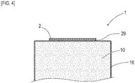
- RFID tag 2 in magnetic marker 1 is arranged on the end face of magnet 10 forming the main body, in a state of having resin-made, sheet-shaped spacer 29 interposed therebetween as in FIG. 4 .
- Metal foil 16 covering the outer peripheral surface of magnet 10 and RFID tag 2 are in a state of being electrically insulated by resin-made spacer 29 forming one example of a plate-shaped intermediate member.
- the above-described magnetic marker 1 is laid in a state of being accommodated in, for example an accommodation hole 31 bored in a road surface 30S, as in FIG. 5 .
- Magnetic marker 1 laid in this manner makes magnetism act exceeding 8 ⁇ T in a height range from 100 mm to 250 mm assumed as an attachment position of magnetic sensor 35 on vehicle 3 side.
- the magnetism exceeding 8 ⁇ T can be measured with high reliability by, for example, an MI (Magneto Impedance) sensor having a measurement range of magnetic flux density of ⁇ 0.6 mT and achieving high sensitivity on the order of 0.02 ⁇ T as a magnetic flux resolution in the measurement range, or the like.
- MI Magnetic Impedance
- metal foil 16 covering the outer peripheral surface of magnet 10 is coupled with antenna 23 ( FIG. 2 ) of RFID tag 2 by electrostatic coupling, electromagnetic coupling, or the like in an electrically non-contact state, and acts so as to amplify electric waves at antenna 23. That is, in magnetic marker 1, metal foil 16 covering the outer peripheral surface of magnet 10 can act as an external antenna of RFID tag 2. Metal foil 16 is useful in improving reliability of wireless communication between tag reader (one example of a reader device) 36 on vehicle 3 side acquiring information from RFID tag 2 and RFID tag 2. Note that while magnetic sensor 35 and tag reader 36 are depicted as separate bodies in FIG. 5 , magnetic sensor 35 and tag reader 36 may be integrated as a unit.
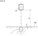
- a distance B ( FIG. 6 ) where tag reader 36 positioned in a vertical direction above the magnetic marker can communicate with an error rate smaller than 1% is indicated as a communication distance.
- a comparison regarding the above-described communication distance is indicated between a state in which the magnetic marker is buried so that a distance A ( FIG. 6 ) from road surface 30S to the upper end face is 10 mm (buried state) and a single-body state.
- Magnetic marker 1 of the present embodiment with the outer peripheral surface covered with metal foil 16 even in the state of being buried in road surface 30S, the degree of impairing the communication characteristic of RFID tag 2 is small.
- Magnetic marker 1 of the present embodiment with RFID tag 2 attached thereto can perform communication with vehicle 3 side with high reliability and can provide more information to the vehicle side.
- resin-made spacer 29 is arranged between the end face of magnet 10 and RFID tag 2 (refer to FIG. 4 ) and metal foil 16 and RFID tag 2 are in a state of not making electrical contact with each other.
- a configuration in which antenna 23 of RFID tag 2 and metal foil 16 make electrical contact with each other may be adopted.
- the electrical contact state refers to a state in which, for example, antenna 23 makes contact with metal foil 16 directly or indirectly via a conductor and the direct-current resistance therebetween becomes almost zero.
- an electrical non-contact state refers to a state in which, for example, antenna 23 does not make contact with metal foil 16 and the direct-current resistance therebetween is sufficiently large.
- a tag with antenna 282 (second antenna) having a U-shaped cross section retained in resin may be used as RFID tag 2, as in FIG. 7 and FIG. 8 .
- Antenna 282 having a U-shaped cross section is processed by, for example, folding a metal-made, strap-like flat plate into a U shape.
- RFID tag 2 of the drawing is created by, for example, insert molding of injecting a resin material into the perimeter of antenna 282 for curing, or the like.
- the state is such that metal surfaces of antenna 282 are exposed on both front and back surfaces.
- sheet-shaped tag 281 is retained in resin so as to face a U-shaped inner bottom surface (inner peripheral surface) formed by the antenna 282.
- Tag 281 has an IC chip mounted on the surface of the tag sheet and is provided with an antenna pattern, and is similar in configuration to the RFID tag exemplarily depicted in FIG. 2 .
- a gap is provided between tag 281 and antenna 282, which are in a state of not making electrical contact with each other via resin and being electrically insulated from each other.
- an antenna (antenna electrically extended from the IC chip forming a circuit) incorporated in tag 281 is coupled to the antenna 282 having a U-shaped cross section by electrostatic coupling, electromagnetic coupling, or the like in an electrically non-contact state.
- Antenna 282 relays electric waves transmitted and received by the antenna of tag 281 and functions as an antenna which amplifies the electric waves to enhance radio field intensity.
- this RFID tag 2 is attached to the end face of magnet 10 forming the main body via the surface where the metal surface of antenna 282 having a U-shaped cross section is exposed.
- metal foil 16 is formed, and antenna 282 having a U-shaped cross section is in a state of making electrical contact with metal foil 16. Therefore, in magnetic marker 1 of FIG. 8 , metal foil 16 together with antenna 282 functions as an external antenna of the antenna incorporated in tag 281. Note that as the arrangement position in RFID tag 2, it is only required that tag 281 be positioned on the inner perimeter of antenna 282 having a U-shaped cross section.
- Sheet-shaped tag 281 may be retained so as not to face the U-shaped bottom surface formed by antenna 282 but to face either one of its inner peripheral surfaces facing each other. Furthermore, sheet-shaped tag 281 may be retained so as to be orthogonal to the U-shaped bottom surface and also orthogonal to the inner peripheral surfaces facing each other.
- the antenna incorporated in tag 281 and antenna 282 may be electrically contacted with each other.
- the antenna incorporated in tag 281 makes electrical contact with metal foil 16 via antenna 282.
- RFID tag 2 is arranged on the end face of magnetic marker 1 covered with metal foil 16 in the present embodiment, RFID tag 2 may be arranged on the outer peripheral side surface of magnetic marker 1. In this case, RFID tag 2 is preferably arranged on a portion of the outer peripheral side surface of magnetic marker 1 covered with the metal foil. Furthermore, RFID tag 2 may also be preferably buried inside magnet 10 by insert molding or the like. Also in this case, metal foil 16 provided on the outer periphery of magnet 10 can act as an external antenna of RFID tag 2.
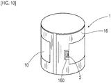
- metal foil 16 of FIG. 9 having a loop shape may also be wound around the outer peripheral side surface of magnet 10 forming the main body as in FIG. 10 .
- RFID tag 2 having an antenna incorporated therein is preferably arranged on an inner peripheral side of loop-shaped metal foil 16.
- metal foil 16 is coupled to the antenna incorporated in RFID tag 2 by electrostatic coupling, electromagnetic coupling, or the like, and metal foil 16 functions as an external antenna of RFID tag 2.
- RFID tag 2 is preferably brought close to metal foil 16. By bringing it close, the degree of coupling between metal foil 16 forming a conductive layer and the antenna incorporated in RFID tag 2 can be increased, and wireless communication sensitivity of RFID tag 2 can be improved. Furthermore, it is also preferable that part of an inner peripheral edge part of loop-shaped metal foil 16 is dented to an outer peripheral side to form recessed part 160 and RFID tag 2 is arranged in this recessed part 160. With RFID tag 2 arranged in the recessed part 160 in this manner, the antenna incorporated in this RFID tag 2 can be surrounded by metal foil 16.
- a ratio of a portion close to metal foil 16 forming a conductive layer can be increased. If this ratio can be increased, the degree of coupling between metal foil 16 and the antenna incorporated in RFID tag 2 can be enhanced.
- RFID tag 2 is arranged so that not the surface where IC chip 27 is mounted but the back surface on a tag sheet 20 side makes contact with the metal foil 16.
- Tag sheet 20 of RFID tag 2 is formed of a PET film or the like with a low electrical conductivity. If the mount surface of IC chip 27 is set outside as described above, the electrically insulated state between metal foil 16 and RFID tag 2 can be kept.
- magnetic marker 1 exemplarily depicted has a columnar shape
- a sheet-shaped thin magnetic marker may be used.
- metal foil 16 is formed on at least part of the surface and RFID tag 2 is arranged on a surface side of that metal foil 16.
- a magnetic marker system in which a buried magnetic marker and a magnetic marker arranged on the road surface have different specifications of electric waves, such as specifications of frequency (carrier frequency) of carrier waves when RFID tag 2 wirelessly transmits information or specifications of carrier frequency when electric power is fed to RFID tag 2.
- the frequency of electric waves (such as carrier waves) transmitted from RFID tag 2 is preferably set to be shifted by the shift amount of the frequency.
- the carrier frequency when operating power is transmitted is preferably set to be shifted by the shift amount of the frequency. If the frequency of carrier waves is shifted by the amount of the shift phenomenon, the error rate when information is transmitted can be reduced, and power transmission efficiency can be improved.
- code information indicating whether the magnetic marker is a buried magnetic marker or a magnetic marker arranged on the road surface is included in information to be transmitted from RFID tag 2.
- a head magnetic marker positioned on the most upstream side in the traveling direction of the vehicle
- an RFID tag which transmits code information indicating the head of the buried section or the road-surface arrangement section may also be combined.
- information identifying whether the section is a buried section where magnetic markers are buried or a road-surface arrangement section where magnetic markers are arranged on the road surface may also be included in a map database included in the vehicle side or the like.
- Tag reader 36 is preferably provided with, for example, a frequency switching part which selectively sets any of carrier frequencies of a plurality of types.
- tag reader 36 preferably switches the carrier frequency at the time of power transmission.
- this difference in reception frequency is a difference in frequency of electric waves (carrier waves) received by tag reader 36 side, a difference in frequency of electric waves (carrier waves) received by RFID tag 2 side, or the like.
- a columnar-shaped magnetic marker may be placed or the like on the road surface, or a sheet-shaped magnetic marker may be buried in the road surface.
- the degree of the above-described shift phenomenon varies in accordance with the burying depth of the magnetic marker and the type of a burying material.
- buried-type magnetic markers of a plurality of types with different settings of the frequency of transmission electric waves may be prepared in accordance with the burying depth and the burying material.
- a resin layer made of a resin material may be provided on the outer periphery of magnet 10 and a conductive layer may be further provided on the outside of the resin layer.
- the outer periphery of magnet 10 provided with metal foil 16 forming a conductive layer is coated with a resin material and RFID tag 2 may be arranged on the surface of the coating layer.
- a conductive layer may be formed by metal plating. That is, the conductive layer may be a plated layer formed by metal plating.
- the magnetic marker may have a magnet accommodated in a metal container.
- a coating layer made of a resin material is preferably provided on the outer perimeter of the metal container. If a conductive layer (such as metal foil) is formed on the outer periphery of this coating layer, an electrical contact between the metal container forming the main body of the magnetic marker and the conductive layer is avoided, and a state in which both do not have electrical continuity can be achieved.
Landscapes
- Engineering & Computer Science (AREA)
- Physics & Mathematics (AREA)
- General Physics & Mathematics (AREA)
- Theoretical Computer Science (AREA)
- Microelectronics & Electronic Packaging (AREA)
- Computer Hardware Design (AREA)
- Health & Medical Sciences (AREA)
- Toxicology (AREA)
- Civil Engineering (AREA)
- Electromagnetism (AREA)
- General Engineering & Computer Science (AREA)
- Architecture (AREA)
- Computer Networks & Wireless Communication (AREA)
- Structural Engineering (AREA)
- General Health & Medical Sciences (AREA)
- Artificial Intelligence (AREA)
- Computer Vision & Pattern Recognition (AREA)
- Road Signs Or Road Markings (AREA)
- Control Of Position, Course, Altitude, Or Attitude Of Moving Bodies (AREA)
- Traffic Control Systems (AREA)
- Near-Field Transmission Systems (AREA)
Abstract
Description
- The present invention relates to a magnetic marker to be laid in a road.
- Conventionally, a magnetic marker to be laid in a road detectably by a magnetic sensor on a vehicle side has been known (for example, refer to Patent Literature 1). By using the magnetic marker, there is a possibility that in addition to, for example, various driving assists such as automatic steering control and lane departure warning using the magnetic marker laid along a lane, automatic driving can be achieved.
- Patent Literature 1: Japanese Unexamined Patent Application Publication No.
2005-202478 - However, information that can be acquired by detection of a magnetic marker indicates the presence or absence of the magnetic marker, the shift amount of a vehicle in a width direction with respect to the magnetic marker, information about whether a magnetic polarity indicates the North Pole or the South Pole, and so forth. There is a problem in which the amount and type of information that can be acquired from the magnetic marker side cannot be said as sufficient.
- The present invention was made in view of the above-described conventional problem, and is to provide a magnetic marker that can provide more information with high reliability.
- One aspect of the present invention resides in a magnetic marker to be laid in a road, the magnetic marker including,
a wireless tag including a circuit which processes information transmitted and received by wireless communication and a first antenna provided to extend electrically from the circuit, and
a conductive layer provided on at least part of an outer peripheral surface of a main body forming a magnetism generation source, the conductive layer being not electrically continuous with the main body. - One aspect of the present invention resides in a magnetic marker system including the above-described magnetic marker which retains the wireless tag, wherein
frequency specifications of electric waves transmitted from the wireless tag are different between the magnetic marker laid as being buried at a position deep from a road surface of the road and the magnetic marker laid as being arranged on the road surface. - The magnetic marker according to the present invention includes the wireless tag. With the magnetic marker including the wireless tag, more information can be provided to a vehicle side by using wireless communication. In this magnetic marker, the conductive layer with conductivity is formed on at least part of the outer peripheral surface of the main body. The conductive layer functions as an external antenna of the wireless tag and effectively acts to improve reliability of wireless communication.
- In the magnetic marker system according to the present invention, there are a buried magnetic marker and a magnetic marker arranged on the road surface. Between the buried magnetic marker and the magnetic marker arranged on the road surface, there is a difference as to whether a burying material such as, for example, resin or asphalt, is included in a route of electric waves transmitted from the wireless tag. If the burying material is present in the route of electric waves, a shift phenomenon, in which the frequency of passing electric waves is shifted can occur due to a difference between the permittivity of the burying material and the permittivity of air, or the like. If the frequency of electric waves transmitted from the wireless tag is set in view of the occurrence of this shift phenomenon, reliability of transmission between the wireless tag and the counterpart can be improved.
-
-
FIG. 1 is a diagram depicting a magnetic marker. -
FIG. 2 is a diagram depicting an RFID tag. -
FIG. 3 is a diagram depicting a developed shape of a metal foil. -
FIG. 4 is a sectional diagram depicting an attachment structure of the RFID tag. -
FIG. 5 is a diagram depicting a laying mode of the magnetic marker. -
FIG. 6 is a descriptive diagram of a communication distance. -
FIG. 7 is a perspective diagram depicting a sectional structure of another RFID tag. -
FIG. 8 is a perspective diagram depicting another magnetic marker. -
FIG. 9 is a diagram depicting another developed shape of the metal foil. -
FIG. 10 is a perspective diagram depicting another magnetic marker. - Embodiments of the present invention are specifically described by using the following examples.
- The present embodiment is an example regarding
magnetic marker 1 including RFID (Radio Frequency IDentification, wireless tag) 2. Details of this are described by usingFIG. 1 to FIG. 10 . -
Magnetic marker 1 is a marker for a road to be arranged, for example, along the center of a lane.Magnetic marker 1 is used for various vehicle controls such as, for example, lane departure warning, lane keep assist, and automatic driving.Magnetic marker 1 ofFIG. 1 exemplarily depicted has a columnar shape having a diameter (D) of 20 mm and a height (H) of 28 mm. In thismagnetic marker 1, sheet-shaped RFID tag 2 is arranged and laminated on one end face ofcolumnar magnet 10 forming a main body. - First,
RFID tag 2 is, as inFIG. 2 , an electronic part with IC (Integrated Circuit)chip 27 mounted on a surface oftag sheet 20, which is a sheet-shaped member.RFID tag 2 is configured to operate by electric power externally supplied by wireless transmission and to wirelessly transmit information stored inIC chip 27. -
Tag sheet 20 is a sheet-shaped member cut out from a PET (PolyEthylene Terephthalate) film. On the surface oftag sheet 20,antenna pattern 231 is formed, which is a conductive-ink printed pattern formed of silver paste.Antenna pattern 231 has a loop shape with a notch, and a chip arrangement region (not depicted) for arrangingIC chip 27 is formed at a notched portion. WhenIC chip 27 is jointed totag sheet 20,antenna pattern 231 is electrically connected toIC chip 27. With this,antenna 23 formed byantenna pattern 231 becomes in a state of electrically extending fromIC chip 27 forming a circuit for processing information transmitted and received via wireless communication. - Antenna (first antenna) 23 formed by
antenna pattern 231 has both of a role as power-feeding antenna where an exciting current is generated by electromagnetic induction from outside and a role as a communication antenna for wireless transmission of information. Note that as a conductive ink forprinting antenna pattern 231, it is possible to use, in addition to silver paste, graphite paste, silver chloride paste, copper paste, nickel paste and so forth. Furthermore, it is also possible to formantenna pattern 231 by copper etching or the like. -
IC chip 27 is an electronic part withsemiconductor element 271 including a ROM (Read Only Memory) and a RAM (Random Access Memory) as memory means and so forth mounted on the surface of sheet-shaped base material 273.RFID tag 2 is fabricated by affixing thisIC chip 27 onto the surface of the above-describedtag sheet 20. To affixIC chip 27 of an interposer type provided with an electrode not depicted, various jointing methods can be adopted such as ultrasonic jointing, or swaging jointing in addition to a conductive bonding material. - As
tag sheet 20 andbase material 273 described above, a resin film made of polyethylene (PE), polyethylene terephthalate (PET), polypropylene (PP), or the like, paper, or the like can be adopted. The above-describedIC chip 27 may besemiconductor element 271 itself or a chip withsemiconductor element 271 packaged by a plastic resin or the like. - Magnet 10 (
FIG. 1 ) forming the main body (magnetism generation source) ofmagnetic marker 1 is an isotropic ferrite plastic magnet formed by dispersing a magnetic powder of iron oxide as a magnetic material in a polymer material (non-conductive material) as a base material.Magnet 10 with magnetic powder dispersed in the non-conductive polymer material has an electrical characteristic of a low electrical conductivity and a magnetic characteristic of a maximum energy product (BHmax)=6.4 kJ/m3. -
Magnetic marker 1 including thismagnet 10 has a magnetic flux density Gs of the surface of 45 mT (millitesla). The magnetic flux density of 45 mT is equal to or smaller than the magnetic flux density of the surface of, for example, a magnetic sheet for use as being affixed to a white board in an office or the like, a door of a refrigerator at home, or the like. - Part of the outer peripheral surface of
magnet 10 is covered withmetal foil 16 forming one example of a conductive layer with conductivity. Thismetal foil 16 is made of aluminum and has a thickness of 0.03 mm. As described above, sincemagnet 10 has a low electrical conductivity,metal foil 16 is in a state of being not electrically continuous with the main body ofmagnet 10. - To clarify a range where a conductive layer is formed by
metal foil 16, the shape ofmetal foil 16 developed on a plane is depicted inFIG. 3 . In the drawing, a cylindrical portion corresponding to the outer peripheral side surface of themagnetic marker 1 is depicted, with one portion in a circumferential direction being cut by a broken line. As in the drawing, inmagnetic marker 1, the conductive layer bymetal foil 16 is formed over one end face and the entire outer peripheral side surface ofmagnet 10 forming a columnar shape. The above-describedRFID tag 2 is arranged and laminated on the end face ofmagnet 10 provided withmetal foil 16. -
RFID tag 2 inmagnetic marker 1 is arranged on the end face ofmagnet 10 forming the main body, in a state of having resin-made, sheet-shapedspacer 29 interposed therebetween as inFIG. 4 .Metal foil 16 covering the outer peripheral surface ofmagnet 10 andRFID tag 2 are in a state of being electrically insulated by resin-madespacer 29 forming one example of a plate-shaped intermediate member. - The above-described
magnetic marker 1 is laid in a state of being accommodated in, for example anaccommodation hole 31 bored in aroad surface 30S, as inFIG. 5 .Magnetic marker 1 laid in this manner makes magnetism act exceeding 8 µT in a height range from 100 mm to 250 mm assumed as an attachment position ofmagnetic sensor 35 on vehicle 3 side. The magnetism exceeding 8 µT can be measured with high reliability by, for example, an MI (Magneto Impedance) sensor having a measurement range of magnetic flux density of ±0.6 mT and achieving high sensitivity on the order of 0.02 µT as a magnetic flux resolution in the measurement range, or the like. - In this
magnetic marker 1,metal foil 16 covering the outer peripheral surface ofmagnet 10 is coupled with antenna 23 (FIG. 2 ) ofRFID tag 2 by electrostatic coupling, electromagnetic coupling, or the like in an electrically non-contact state, and acts so as to amplify electric waves atantenna 23. That is, inmagnetic marker 1,metal foil 16 covering the outer peripheral surface ofmagnet 10 can act as an external antenna ofRFID tag 2.Metal foil 16 is useful in improving reliability of wireless communication between tag reader (one example of a reader device) 36 on vehicle 3 side acquiring information fromRFID tag 2 andRFID tag 2. Note that whilemagnetic sensor 35 andtag reader 36 are depicted as separate bodies inFIG. 5 ,magnetic sensor 35 andtag reader 36 may be integrated as a unit. - Here, to signify an advantageous communication characteristic of
magnetic marker 1 of the present embodiment, a comparison results with the magnetic marker withoutmetal foil 16 are depicted in Table 1.[Table 1] COMMUNICATION DISTANCE AS A SINGLE BODY COMMUNICATION DISTANCE UNDER BURIED STATE MAGNETIC MARKER (WITH METAL FOIL) 0.60 m 0.51 m MAGNETIC MARKER (WITHOUT METAL FOIL) 0.53 m 0.08 m - In Table 1, a distance B (
FIG. 6 ) wheretag reader 36 positioned in a vertical direction above the magnetic marker can communicate with an error rate smaller than 1% is indicated as a communication distance. And, a comparison regarding the above-described communication distance is indicated between a state in which the magnetic marker is buried so that a distance A (FIG. 6 ) fromroad surface 30S to the upper end face is 10 mm (buried state) and a single-body state. - As evident from Table 1, as for the magnetic marker in the single-body state without being buried in asphalt forming
road surface 30S, a sufficient communication distance can be achieved with respect to the attachment height of the magnetic sensor of 100 mm to 250 mm in the vehicle, irrespective of the presence or absence ofmetal foil 16. On the other hand, in the state of being buried inroad surface 30S, the communication distance of the magnetic marker without themetal foil 16 is significantly short. By contrast,magnetic marker 1 of the present embodiment includingmetal foil 16 can keep the communication distance even in the buried state. - In this manner, in
magnetic marker 1 of the present embodiment with the outer peripheral surface covered withmetal foil 16, even in the state of being buried inroad surface 30S, the degree of impairing the communication characteristic ofRFID tag 2 is small.Magnetic marker 1 of the present embodiment withRFID tag 2 attached thereto can perform communication with vehicle 3 side with high reliability and can provide more information to the vehicle side. - Note that in
magnetic marker 1, resin-madespacer 29 is arranged between the end face ofmagnet 10 and RFID tag 2 (refer toFIG. 4 ) andmetal foil 16 andRFID tag 2 are in a state of not making electrical contact with each other. In place of this configuration, a configuration in whichantenna 23 ofRFID tag 2 andmetal foil 16 make electrical contact with each other may be adopted. Here, the electrical contact state refers to a state in which, for example,antenna 23 makes contact withmetal foil 16 directly or indirectly via a conductor and the direct-current resistance therebetween becomes almost zero. On the other hand, an electrical non-contact state refers to a state in which, for example,antenna 23 does not make contact withmetal foil 16 and the direct-current resistance therebetween is sufficiently large. - Note that, as
RFID tag 2, as inFIG. 7 andFIG. 8 , a tag with antenna 282 (second antenna) having a U-shaped cross section retained in resin may be used.Antenna 282 having a U-shaped cross section is processed by, for example, folding a metal-made, strap-like flat plate into a U shape.RFID tag 2 of the drawing is created by, for example, insert molding of injecting a resin material into the perimeter ofantenna 282 for curing, or the like. In thisRFID tag 2, the state is such that metal surfaces ofantenna 282 are exposed on both front and back surfaces. Furthermore, in thisRFID tag 2, sheet-shapedtag 281 is retained in resin so as to face a U-shaped inner bottom surface (inner peripheral surface) formed by theantenna 282.Tag 281 has an IC chip mounted on the surface of the tag sheet and is provided with an antenna pattern, and is similar in configuration to the RFID tag exemplarily depicted inFIG. 2 . - In
RFID tag 2 ofFIG. 7 andFIG. 8 , a gap is provided betweentag 281 andantenna 282, which are in a state of not making electrical contact with each other via resin and being electrically insulated from each other. In thisRFID tag 2, an antenna (antenna electrically extended from the IC chip forming a circuit) incorporated intag 281 is coupled to theantenna 282 having a U-shaped cross section by electrostatic coupling, electromagnetic coupling, or the like in an electrically non-contact state.Antenna 282 relays electric waves transmitted and received by the antenna oftag 281 and functions as an antenna which amplifies the electric waves to enhance radio field intensity. - As in
FIG. 7 andFIG. 8 , thisRFID tag 2 is attached to the end face ofmagnet 10 forming the main body via the surface where the metal surface ofantenna 282 having a U-shaped cross section is exposed. On the end face ofmagnet 10 forming the attachment surface ofRFID tag 2,metal foil 16 is formed, andantenna 282 having a U-shaped cross section is in a state of making electrical contact withmetal foil 16. Therefore, inmagnetic marker 1 ofFIG. 8 ,metal foil 16 together withantenna 282 functions as an external antenna of the antenna incorporated intag 281. Note that as the arrangement position inRFID tag 2, it is only required that tag 281 be positioned on the inner perimeter ofantenna 282 having a U-shaped cross section. Sheet-shapedtag 281 may be retained so as not to face the U-shaped bottom surface formed byantenna 282 but to face either one of its inner peripheral surfaces facing each other. Furthermore, sheet-shapedtag 281 may be retained so as to be orthogonal to the U-shaped bottom surface and also orthogonal to the inner peripheral surfaces facing each other. - Furthermore, as for
RFID tag 2 depicted inFIG. 7 andFIG. 8 in which a gap is provided betweentag 281 andantenna 282, which are both in an electrically insulated state via resin, the antenna incorporated intag 281 andantenna 282 may be electrically contacted with each other. In this case, the antenna incorporated intag 281 makes electrical contact withmetal foil 16 viaantenna 282. - While
RFID tag 2 is arranged on the end face ofmagnetic marker 1 covered withmetal foil 16 in the present embodiment,RFID tag 2 may be arranged on the outer peripheral side surface ofmagnetic marker 1. In this case,RFID tag 2 is preferably arranged on a portion of the outer peripheral side surface ofmagnetic marker 1 covered with the metal foil. Furthermore,RFID tag 2 may also be preferably buried insidemagnet 10 by insert molding or the like. Also in this case,metal foil 16 provided on the outer periphery ofmagnet 10 can act as an external antenna ofRFID tag 2. - While
magnetic marker 1 with one end face and the outer peripheral side surface covered with themetal foil 16 is exemplarily described in the present embodiment,metal foil 16 ofFIG. 9 having a loop shape may also be wound around the outer peripheral side surface ofmagnet 10 forming the main body as inFIG. 10 . Inmagnetic marker 1 withmetal foil 16 ofFIG. 9 wound around the outer peripheral side surface,RFID tag 2 having an antenna incorporated therein is preferably arranged on an inner peripheral side of loop-shapedmetal foil 16. In this case,metal foil 16 is coupled to the antenna incorporated inRFID tag 2 by electrostatic coupling, electromagnetic coupling, or the like, andmetal foil 16 functions as an external antenna ofRFID tag 2. - Note that to arrange
RFID tag 2 on the inner peripheral side of loop-shapedmetal foil 16,RFID tag 2 is preferably brought close tometal foil 16. By bringing it close, the degree of coupling betweenmetal foil 16 forming a conductive layer and the antenna incorporated inRFID tag 2 can be increased, and wireless communication sensitivity ofRFID tag 2 can be improved. Furthermore, it is also preferable that part of an inner peripheral edge part of loop-shapedmetal foil 16 is dented to an outer peripheral side to form recessedpart 160 andRFID tag 2 is arranged in this recessedpart 160. WithRFID tag 2 arranged in the recessedpart 160 in this manner, the antenna incorporated in thisRFID tag 2 can be surrounded bymetal foil 16. In this case, of the outer perimeter of the antenna incorporated inRFID tag 2, a ratio of a portion close tometal foil 16 forming a conductive layer can be increased. If this ratio can be increased, the degree of coupling betweenmetal foil 16 and the antenna incorporated inRFID tag 2 can be enhanced. - While the structure in the present embodiment is such that
spacer 29 is interposed betweenRFID tag 2 andmetal foil 16 coveringmagnetic marker 1,spacer 29 may be omitted. In this case,RFID tag 2 is arranged so that not the surface whereIC chip 27 is mounted but the back surface on atag sheet 20 side makes contact with themetal foil 16.Tag sheet 20 ofRFID tag 2 is formed of a PET film or the like with a low electrical conductivity. If the mount surface ofIC chip 27 is set outside as described above, the electrically insulated state betweenmetal foil 16 andRFID tag 2 can be kept. - While
magnetic marker 1 exemplarily depicted has a columnar shape, a sheet-shaped thin magnetic marker may be used. As for the sheet-shaped magnetic marker, it is preferable thatmetal foil 16 is formed on at least part of the surface andRFID tag 2 is arranged on a surface side of thatmetal foil 16. - While it is easy for, by way of example, columnar-shaped
magnetic marker 1 or the like, to adopt a laying mode of being buried at a position deep from the road surface forming a surface of a road, it is easy for the sheet-shaped magnetic marker to adopt a laying mode of being arranged on the road surface by being affixed to or placed on the road surface, or the like. Meanwhile, when the magnetic marker is buried, in a route of electric waves fromRFID tag 2 to tagreader 36, a medium is present, such as resin or asphalt (pavement material) for the magnetic marker to be buried. In this case, there is a possibility of occurrence of a shift phenomenon in which the frequency of passing electric waves is shifted due to, for example, a difference between the permittivity of the medium such as resin or asphalt and the permittivity of air. On the other hand, if the magnetic marker is affixed to the road surface or the like, the medium such as resin or asphalt is hardly present in the route of electric waves, and thus the fear of the frequency shift phenomenon as described above is less. Therefore, if the frequency specifications (specifications of frequency of electric waves such as carrier waves) ofRFID tag 2 andtag reader 36 are the same irrespective of whether the frequency shift phenomenon tends to occur because the magnetic marker is buried in the road surface or the magnetic marker is arranged on the road surface and has less fear of the shift phenomenon, there is a fear that a difference in frequency of electric waves received by thetag reader 36 may occur or a difference in frequency of electric waves received by theRFID tag 2 may occur. - Thus, a magnetic marker system is preferable in which a buried magnetic marker and a magnetic marker arranged on the road surface have different specifications of electric waves, such as specifications of frequency (carrier frequency) of carrier waves when
RFID tag 2 wirelessly transmits information or specifications of carrier frequency when electric power is fed toRFID tag 2. As for the buried magnetic marker, in consideration of the above-described frequency shift phenomenon, the frequency of electric waves (such as carrier waves) transmitted fromRFID tag 2 is preferably set to be shifted by the shift amount of the frequency. Also, on atag reader 36 side, the carrier frequency when operating power is transmitted (power supply by wireless communication) is preferably set to be shifted by the shift amount of the frequency. If the frequency of carrier waves is shifted by the amount of the shift phenomenon, the error rate when information is transmitted can be reduced, and power transmission efficiency can be improved. - It is also preferable, for example, that code information indicating whether the magnetic marker is a buried magnetic marker or a magnetic marker arranged on the road surface is included in information to be transmitted from
RFID tag 2. For example, for a head magnetic marker (positioned on the most upstream side in the traveling direction of the vehicle) in a buried section where magnetic markers are buried or in a road-surface arrangement section where magnetic markers are arranged on the road surface, an RFID tag which transmits code information indicating the head of the buried section or the road-surface arrangement section may also be combined. Furthermore, for example, information identifying whether the section is a buried section where magnetic markers are buried or a road-surface arrangement section where magnetic markers are arranged on the road surface may also be included in a map database included in the vehicle side or the like. -
Tag reader 36 is preferably provided with, for example, a frequency switching part which selectively sets any of carrier frequencies of a plurality of types. When the magnetic marker is identified as a buried magnetic marker or a magnetic marker arranged on the road surface or the section is identified as the above-described buried section or road-surface arrangement section,tag reader 36 preferably switches the carrier frequency at the time of power transmission. - When the setting of the frequency (frequency specifications) is changed in accordance with the laying mode of the magnetic marker, the above-described adverse effect due to the shift phenomenon can be avoided before it happens. In this case, the difference in reception frequency of electric waves due to the difference in laying mode as to whether the magnetic marker is a buried magnetic marker or a magnetic marker arranged on the road surface can be brought close to zero. As described above, this difference in reception frequency is a difference in frequency of electric waves (carrier waves) received by
tag reader 36 side, a difference in frequency of electric waves (carrier waves) received byRFID tag 2 side, or the like. - Note that the laying mode of the magnetic marker is not limited to the above. A columnar-shaped magnetic marker may be placed or the like on the road surface, or a sheet-shaped magnetic marker may be buried in the road surface.
- Furthermore, the degree of the above-described shift phenomenon varies in accordance with the burying depth of the magnetic marker and the type of a burying material. Thus, buried-type magnetic markers of a plurality of types with different settings of the frequency of transmission electric waves may be prepared in accordance with the burying depth and the burying material.
- While the conductive layer by
metal foil 16 is provided directly on the outer peripheral surface ofmagnet 10 forming the main body in the present embodiment, a resin layer made of a resin material may be provided on the outer periphery ofmagnet 10 and a conductive layer may be further provided on the outside of the resin layer. Alternatively, the outer periphery ofmagnet 10 provided withmetal foil 16 forming a conductive layer is coated with a resin material andRFID tag 2 may be arranged on the surface of the coating layer. - In place of the conductive layer formed of
metal foil 16, a conductive layer may be formed by metal plating. That is, the conductive layer may be a plated layer formed by metal plating. - The magnetic marker may have a magnet accommodated in a metal container. In this case, a coating layer made of a resin material is preferably provided on the outer perimeter of the metal container. If a conductive layer (such as metal foil) is formed on the outer periphery of this coating layer, an electrical contact between the metal container forming the main body of the magnetic marker and the conductive layer is avoided, and a state in which both do not have electrical continuity can be achieved.
- In the foregoing, specific examples of the present invention are described in detail as in the embodiments, these specific examples merely disclose examples of technology included in the scope of claims for patent. Needless to say, the scope of claims for patent should not be restrictively construed based on the configuration, numerical values and so forth of the specific examples. The scope of claims for patent includes techniques acquired by variously modifying, changing, or combining as appropriate the above-described specific examples by using known techniques, knowledge of a person skilled in the art and so forth.
-
- 1
- magnetic marker
- 10
- magnet (main body)
- 16
- metal foil (conductive layer)
- 2
- RFID tag (wireless tag)
- 20
- tag sheet
- 23
- antenna
- 231
- antenna pattern
- 27
- IC chip (circuit)
- 29
- spacer (intermediate member)
- 3
- vehicle
- 31
- accommodation hole
- 35
- magnetic sensor
- 36
- tag reader
- 30S
- road surface
Claims (10)
- A magnetic marker to be laid in a road, the magnetic marker comprising:a wireless tag including a circuit which processes information transmitted and received by wireless communication and a first antenna provided to extend electrically from the circuit, anda conductive layer provided on at least part of an outer peripheral surface of a main body forming a magnetism generation source, the conductive layer being not electrically continuous with the main body.
- The magnetic marker according to claim 1, wherein
the wireless tag includes a second antenna which relays electric waves transmitted and received by the first antenna, and the second antenna makes electrical contact with the conductive layer. - The magnetic marker according to claim 2, wherein
the second antenna has a U-shaped cross section, and the first antenna is provided so as to be positioned on an inner periphery of the second antenna having the U-shaped cross section. - The magnetic marker according to any one of claims 1 to 3, wherein
the conductive layer is formed to have a loop shape on the outer peripheral surface of the main body. - The magnetic marker according to claim 4, wherein
the wireless tag is arranged on an inner peripheral side of the loop shape formed by the conductive layer. - The magnetic marker according to any one of claims 1 to 5, wherein
the main body is a magnet formed by dispersing a magnetic powder, which is powder made of a magnetic material, in a non-conductive material forming a base material. - The magnetic marker according to any one of claims 1 to 6, wherein
the main body forms a columnar shape, and the conductive layer is formed on at least part of an end face of the columnar-shaped main body. - The magnetic marker according to any one of claims 1 to 7, wherein
the main body forms a columnar shape, and the conductive layer is formed on at least part of an outer peripheral side surface of the columnar-shaped main body. - A magnetic marker system comprising a magnetic marker laid in a road, wherein
the magnetic marker is the magnetic marker according to any one of claims 1 to 6 which retains a wireless tag including a circuit which processes information transmitted and received by wireless communication and a first antenna provided to extend electrically from the circuit, and
frequency specifications of electric waves transmitted from the wireless tag are different between the magnetic marker laid as being buried at a position deep from a road surface of the road and the magnetic marker laid as being arranged on the road surface. - The magnetic marker system according to claim 9, wherein
the system includes a reader device mounted on a vehicle to supply electric power to the wireless tag by wireless communication and read information transmitted from the wireless tag by wireless communication, and
the frequency specifications of electric waves when the reader device supplies electric power are switched in accordance with whether the magnetic marker is laid as being buried or the magnetic marker is laid as being arranged on the road surface.
Applications Claiming Priority (2)
| Application Number | Priority Date | Filing Date | Title |
|---|---|---|---|
| JP2017244294 | 2017-12-20 | ||
| PCT/JP2018/045770 WO2019124196A1 (en) | 2017-12-20 | 2018-12-12 | Magnetic marker and magnetic marker system |
Publications (2)
| Publication Number | Publication Date |
|---|---|
| EP3731149A1 true EP3731149A1 (en) | 2020-10-28 |
| EP3731149A4 EP3731149A4 (en) | 2021-09-01 |
Family
ID=66992674
Family Applications (1)
| Application Number | Title | Priority Date | Filing Date |
|---|---|---|---|
| EP18893066.3A Pending EP3731149A4 (en) | 2017-12-20 | 2018-12-12 | MAGNETIC MARKER AND MAGNETIC MARKER SYSTEM |
Country Status (6)
| Country | Link |
|---|---|
| US (1) | US11238328B2 (en) |
| EP (1) | EP3731149A4 (en) |
| JP (1) | JP7205494B2 (en) |
| CN (1) | CN111492378B (en) |
| SG (1) | SG11202005744SA (en) |
| WO (1) | WO2019124196A1 (en) |
Cited By (1)
| Publication number | Priority date | Publication date | Assignee | Title |
|---|---|---|---|---|
| US11294090B2 (en) * | 2017-03-28 | 2022-04-05 | Aichi Steel Corporation | Marker detection system and marker detection method |
Families Citing this family (9)
| Publication number | Priority date | Publication date | Assignee | Title |
|---|---|---|---|---|
| JP6965815B2 (en) * | 2018-04-12 | 2021-11-10 | 愛知製鋼株式会社 | Marker detection system and operation method of marker detection system |
| US11604476B1 (en) * | 2018-10-05 | 2023-03-14 | Glydways Inc. | Road-based vehicle guidance system |
| JP7092069B2 (en) * | 2019-02-28 | 2022-06-28 | オムロン株式会社 | Manufacturing method of resin parts and resin parts |
| EP4068237A4 (en) * | 2019-11-26 | 2024-01-10 | Aichi Steel Corporation | MAGNETIC MARKER |
| CN114761963A (en) * | 2019-11-26 | 2022-07-15 | 爱知制钢株式会社 | Magnetic marker and method for manufacturing magnetic marker |
| JP2021105255A (en) * | 2019-12-26 | 2021-07-26 | 太平洋セメント株式会社 | Pavement block with marker function |
| JP7538079B2 (en) * | 2021-04-05 | 2024-08-21 | トヨタ自動車株式会社 | Magnetic marker, magnetic marker embedding tool, and magnetic marker embedding method |
| JP7383312B2 (en) * | 2022-03-07 | 2023-11-20 | 日本ミクロン株式会社 | wireless sensor |
| CN117385699B (en) * | 2023-10-11 | 2026-01-02 | 合肥工业大学 | A magnetic asphalt pavement laying device and laying method for driver assistance |
Family Cites Families (33)
| Publication number | Priority date | Publication date | Assignee | Title |
|---|---|---|---|---|
| JP3484495B2 (en) * | 2000-08-23 | 2004-01-06 | 国土交通省国土技術政策総合研究所長 | Magnetic and radio wave combined road marker system |
| US6728629B2 (en) * | 2000-11-24 | 2004-04-27 | National Institute For Land And Infrastructure Management, Ministry Of Land, Infrastructure And Transport | On-road reference point positional data delivery device |
| JP2002294085A (en) * | 2001-03-30 | 2002-10-09 | Dainippon Ink & Chem Inc | Paved road embedded information transmitter / receiver |
| JP3896965B2 (en) * | 2002-01-17 | 2007-03-22 | 三菱マテリアル株式会社 | Reader / writer antenna and reader / writer equipped with the antenna |
| US6992952B2 (en) * | 2002-11-13 | 2006-01-31 | Mitsubishi Materials Corporation | Wrist watch containing internal tag, radio watch, and antenna for wrist watch |
| JP4440570B2 (en) * | 2003-08-29 | 2010-03-24 | 大日本印刷株式会社 | Non-contact data carrier |
| JP2005202478A (en) | 2004-01-13 | 2005-07-28 | Denso Corp | Automated driving system for vehicles |
| US7755484B2 (en) * | 2004-02-12 | 2010-07-13 | Avery Dennison Corporation | RFID tag and method of manufacturing the same |
| JP3803777B2 (en) * | 2005-01-17 | 2006-08-02 | 株式会社ソーシャル・エイド・リサーチ | Storage medium unit and indicator for mounting the storage medium unit |
| DE102005035342B4 (en) * | 2005-06-02 | 2009-04-02 | Wolfgang Nitzsche | Device for wireless emergency signal transmission |
| JP2007199867A (en) * | 2006-01-24 | 2007-08-09 | Mitsubishi Materials Corp | Nameplate with RFID tag |
| US8807438B2 (en) * | 2006-02-22 | 2014-08-19 | Toyo Seikan Kaisha, Ltd. | RFID tag substrate for metal component |
| US20080084311A1 (en) * | 2006-10-06 | 2008-04-10 | Texas Instruments | Inductance enhancement by magnetic material introduction |
| JP4299355B2 (en) * | 2006-12-01 | 2009-07-22 | 株式会社リプロ | Information transmission pile |
| JP4839257B2 (en) * | 2007-04-11 | 2011-12-21 | 株式会社日立製作所 | RFID tag |
| JP4814842B2 (en) * | 2007-06-04 | 2011-11-16 | 株式会社神戸製鋼所 | IC tag unit |
| CN101542831B (en) | 2007-07-09 | 2014-06-25 | 株式会社村田制作所 | Wireless ic device |
| JP5239499B2 (en) * | 2008-05-13 | 2013-07-17 | 戸田工業株式会社 | Composite magnetic antenna and RF tag, metal parts and metal tools provided with the composite magnetic antenna or RF tag |
| JP5065205B2 (en) * | 2008-09-01 | 2012-10-31 | 戸田工業株式会社 | Magnetic field antenna, wireless system and communication system using the same |
| US8350704B2 (en) | 2008-10-03 | 2013-01-08 | Neology, Inc. | Non-transferable radio frequency identification label or tag |
| JP2011245230A (en) * | 2010-05-31 | 2011-12-08 | Onkyo Corp | Speaker for game machine and game machine using the same |
| JP5672874B2 (en) * | 2010-09-09 | 2015-02-18 | 株式会社村田製作所 | Wireless IC tag and RFID system |
| US8078349B1 (en) * | 2011-05-11 | 2011-12-13 | Google Inc. | Transitioning a mixed-mode vehicle to autonomous mode |
| JP5656766B2 (en) * | 2011-08-03 | 2015-01-21 | 太平洋工業株式会社 | Wireless communication system for rotating body |
| US20130162402A1 (en) | 2011-12-27 | 2013-06-27 | Mathias Amann | Apparatus and Method for Providing Product Information |
| KR102041222B1 (en) * | 2012-08-23 | 2019-11-07 | 데쿠세리아루즈 가부시키가이샤 | Antenna device and electronic apparatus |
| JP5696810B2 (en) * | 2012-09-26 | 2015-04-08 | 株式会社村田製作所 | ANTENNA DEVICE AND ELECTRONIC DEVICE HAVING ANTENNA DEVICE |
| DE102013002366A1 (en) * | 2013-02-09 | 2014-08-14 | Servus Intralogistics Gmbh | Method and device for determining the position of transport robots in a widely branched railway network |
| JP6463178B2 (en) * | 2015-03-17 | 2019-01-30 | 株式会社リコー | RFID tag, communication system, and electromagnetic wave control sheet |
| KR101714145B1 (en) * | 2015-04-09 | 2017-03-08 | 현대자동차주식회사 | Apparatus for identifying peripheral vehicle and method thereof |
| JP6620468B2 (en) | 2015-09-01 | 2019-12-18 | 日本製鉄株式会社 | Titanium material and cell member for polymer electrolyte fuel cell containing the same |
| JP6733289B2 (en) * | 2016-04-28 | 2020-07-29 | 愛知製鋼株式会社 | Driving support system |
| CN109074731B (en) | 2016-04-28 | 2021-08-27 | 爱知制钢株式会社 | Magnetic marker and driving support system |
-
2018
- 2018-12-12 US US16/954,445 patent/US11238328B2/en active Active
- 2018-12-12 EP EP18893066.3A patent/EP3731149A4/en active Pending
- 2018-12-12 SG SG11202005744SA patent/SG11202005744SA/en unknown
- 2018-12-12 JP JP2019561010A patent/JP7205494B2/en active Active
- 2018-12-12 WO PCT/JP2018/045770 patent/WO2019124196A1/en not_active Ceased
- 2018-12-12 CN CN201880081590.1A patent/CN111492378B/en active Active
Cited By (1)
| Publication number | Priority date | Publication date | Assignee | Title |
|---|---|---|---|---|
| US11294090B2 (en) * | 2017-03-28 | 2022-04-05 | Aichi Steel Corporation | Marker detection system and marker detection method |
Also Published As
| Publication number | Publication date |
|---|---|
| CN111492378A (en) | 2020-08-04 |
| US11238328B2 (en) | 2022-02-01 |
| CN111492378B (en) | 2024-03-15 |
| EP3731149A4 (en) | 2021-09-01 |
| JP7205494B2 (en) | 2023-01-17 |
| JPWO2019124196A1 (en) | 2021-02-12 |
| US20210089858A1 (en) | 2021-03-25 |
| SG11202005744SA (en) | 2020-07-29 |
| WO2019124196A1 (en) | 2019-06-27 |
Similar Documents
| Publication | Publication Date | Title |
|---|---|---|
| US11238328B2 (en) | Magnetic marker and magnetic marker system | |
| US8902119B2 (en) | Dual polarized UHF antenna | |
| US11280053B2 (en) | Magnetic marker | |
| US11236476B2 (en) | Magnetic marker installation method | |
| US11177555B2 (en) | Back cover for portable terminal and back cover-integrated antenna module including the same | |
| US10910716B2 (en) | RFID infinity antenna | |
| US11970827B2 (en) | Magnetic marker | |
| KR20110002837A (en) | Contactless IC Tag | |
| KR101646173B1 (en) | Shielding unit for a wireless charging receiver module of a PMA wireless charging type and a wireless charging receiver module having the same | |
| US9524602B2 (en) | Compact antenna structure with a coupling device | |
| US11808000B2 (en) | Magnetic marker, and method for manufacturing magnetic marker | |
| JP5630499B2 (en) | Antenna apparatus and wireless communication device | |
| KR20090107154A (en) | antenna | |
| WO2024005104A1 (en) | Magnetic marker | |
| KR20090006098U (en) | antenna |
Legal Events
| Date | Code | Title | Description |
|---|---|---|---|
| STAA | Information on the status of an ep patent application or granted ep patent |
Free format text: STATUS: THE INTERNATIONAL PUBLICATION HAS BEEN MADE |
|
| PUAI | Public reference made under article 153(3) epc to a published international application that has entered the european phase |
Free format text: ORIGINAL CODE: 0009012 |
|
| STAA | Information on the status of an ep patent application or granted ep patent |
Free format text: STATUS: REQUEST FOR EXAMINATION WAS MADE |
|
| 17P | Request for examination filed |
Effective date: 20200616 |
|
| AK | Designated contracting states |
Kind code of ref document: A1 Designated state(s): AL AT BE BG CH CY CZ DE DK EE ES FI FR GB GR HR HU IE IS IT LI LT LU LV MC MK MT NL NO PL PT RO RS SE SI SK SM TR |
|
| AX | Request for extension of the european patent |
Extension state: BA ME |
|
| DAV | Request for validation of the european patent (deleted) | ||
| DAX | Request for extension of the european patent (deleted) | ||
| A4 | Supplementary search report drawn up and despatched |
Effective date: 20210729 |
|
| RIC1 | Information provided on ipc code assigned before grant |
Ipc: G06K 19/077 20060101AFI20210723BHEP Ipc: E01F 11/00 20060101ALI20210723BHEP Ipc: G05D 1/02 20200101ALI20210723BHEP Ipc: G06K 7/10 20060101ALI20210723BHEP Ipc: G06K 19/07 20060101ALI20210723BHEP Ipc: G08G 1/09 20060101ALI20210723BHEP |
|
| STAA | Information on the status of an ep patent application or granted ep patent |
Free format text: STATUS: EXAMINATION IS IN PROGRESS |
|
| 17Q | First examination report despatched |
Effective date: 20220907 |
|
| GRAP | Despatch of communication of intention to grant a patent |
Free format text: ORIGINAL CODE: EPIDOSNIGR1 |
|
| STAA | Information on the status of an ep patent application or granted ep patent |
Free format text: STATUS: GRANT OF PATENT IS INTENDED |
|
| RIC1 | Information provided on ipc code assigned before grant |
Ipc: G06K 19/077 20060101AFI20251105BHEP |
|
| INTG | Intention to grant announced |
Effective date: 20251202 |
|
| RIN1 | Information on inventor provided before grant (corrected) |
Inventor name: YAMAMOTO, MICHIHARU Inventor name: NAGAO, TOMOHIKO Inventor name: AOYAMA, HITOSHI Inventor name: GEMBA, KOEI |
|
| STAA | Information on the status of an ep patent application or granted ep patent |
Free format text: STATUS: THE APPLICATION IS DEEMED TO BE WITHDRAWN |