EP3729179B1 - Waveguide element for a display with reflector surface - Google Patents
Waveguide element for a display with reflector surface Download PDFInfo
- Publication number
- EP3729179B1 EP3729179B1 EP19776864.1A EP19776864A EP3729179B1 EP 3729179 B1 EP3729179 B1 EP 3729179B1 EP 19776864 A EP19776864 A EP 19776864A EP 3729179 B1 EP3729179 B1 EP 3729179B1
- Authority
- EP
- European Patent Office
- Prior art keywords
- waveguide
- display according
- diffractive optical
- reflector surfaces
- optical element
- Prior art date
- Legal status (The legal status is an assumption and is not a legal conclusion. Google has not performed a legal analysis and makes no representation as to the accuracy of the status listed.)
- Active
Links
Images

Classifications
-
- G—PHYSICS
- G02—OPTICS
- G02B—OPTICAL ELEMENTS, SYSTEMS OR APPARATUS
- G02B27/00—Optical systems or apparatus not provided for by any of the groups G02B1/00 - G02B26/00, G02B30/00
- G02B27/0081—Optical systems or apparatus not provided for by any of the groups G02B1/00 - G02B26/00, G02B30/00 with means for altering, e.g. enlarging, the entrance or exit pupil
-
- G—PHYSICS
- G02—OPTICS
- G02B—OPTICAL ELEMENTS, SYSTEMS OR APPARATUS
- G02B27/00—Optical systems or apparatus not provided for by any of the groups G02B1/00 - G02B26/00, G02B30/00
- G02B27/01—Head-up displays
- G02B27/0101—Head-up displays characterised by optical features
-
- G—PHYSICS
- G02—OPTICS
- G02B—OPTICAL ELEMENTS, SYSTEMS OR APPARATUS
- G02B27/00—Optical systems or apparatus not provided for by any of the groups G02B1/00 - G02B26/00, G02B30/00
- G02B27/01—Head-up displays
- G02B27/017—Head mounted
- G02B27/0172—Head mounted characterised by optical features
-
- G—PHYSICS
- G02—OPTICS
- G02B—OPTICAL ELEMENTS, SYSTEMS OR APPARATUS
- G02B27/00—Optical systems or apparatus not provided for by any of the groups G02B1/00 - G02B26/00, G02B30/00
- G02B27/42—Diffraction optics, i.e. systems including a diffractive element being designed for providing a diffractive effect
- G02B27/4272—Diffraction optics, i.e. systems including a diffractive element being designed for providing a diffractive effect having plural diffractive elements positioned sequentially along the optical path
-
- G—PHYSICS
- G02—OPTICS
- G02B—OPTICAL ELEMENTS, SYSTEMS OR APPARATUS
- G02B5/00—Optical elements other than lenses
- G02B5/18—Diffraction gratings
- G02B5/1814—Diffraction gratings structurally combined with one or more further optical elements, e.g. lenses, mirrors, prisms or other diffraction gratings
- G02B5/1819—Plural gratings positioned on the same surface, e.g. array of gratings
-
- G—PHYSICS
- G02—OPTICS
- G02B—OPTICAL ELEMENTS, SYSTEMS OR APPARATUS
- G02B27/00—Optical systems or apparatus not provided for by any of the groups G02B1/00 - G02B26/00, G02B30/00
- G02B27/01—Head-up displays
- G02B27/0101—Head-up displays characterised by optical features
- G02B2027/0123—Head-up displays characterised by optical features comprising devices increasing the field of view
- G02B2027/0125—Field-of-view increase by wavefront division
-
- G—PHYSICS
- G02—OPTICS
- G02B—OPTICAL ELEMENTS, SYSTEMS OR APPARATUS
- G02B27/00—Optical systems or apparatus not provided for by any of the groups G02B1/00 - G02B26/00, G02B30/00
- G02B27/01—Head-up displays
- G02B27/017—Head mounted
- G02B27/0172—Head mounted characterised by optical features
- G02B2027/0174—Head mounted characterised by optical features holographic
Definitions
- the invention relates to waveguide displays which can be used in personal display devices, such as head-mounted displays (HMDs) and head-up displays (HUDs).
- Such displays typically comprise a waveguide and at least one diffractive optical element, such as a grating, arranged onto or into the waveguide.
- Waveguides are key image-forming elements in many modern personal display devices.
- the image to be displayed can be coupled into and out of the waveguide, as well as modified within the waveguide, using diffractive gratings arranged in the main plane of the waveguide, typically on its surface.
- diffractive gratings arranged in the main plane of the waveguide, typically on its surface.
- an in-coupling grating for coupling an image from a projector into the waveguide
- EPE exit pupil expander
- gratings for expanding the light field in one or more in-plane dimensions of the waveguide
- an out-coupling grating which couples the light field out of the waveguide to the user's eye.
- Gratings can be designed to perform optical functions inside the waveguide, just like the exit pupil expansion function of an EPE.
- gratings require considerable surface area, which is very limited in practical display devices, in near-to-the-eye devices (NEDs).
- US 2015/0141704 A1 discloses waveguides with additional reflector surfaces inside the waveguide, which are suitable tilted or curved, when seen in a cross-sectional plane of the waveguide.
- the reflector surfaces facilitate out-coupling of light from the waveguide.
- US-A1-2014268867 furthermore discloses a waveguide element for display comprising an outcoupling grating and two curved reflectors.
- a particular aim is to provide a solution that saves surface area of the waveguide.
- the reflector surface is a planar surface, either perpendicular or moderately (e.g. 1-25 degrees) tilted with respect to the waveguide plane or tilted with respect to that plane.
- the present reflector surface has a shape and orientation in which the surface is capable of redirecting propagating rays within the waveguide, as opposed to coupling light into or out of the waveguide through one of the main surfaces thereof.
- the reflector surface is curved in the waveguide plane (when inspected in the plane of the main surfaces) and/or a plane perpendicular to that plane.
- it may serve as a mirror lens.
- the reflector surface may be a fully or partially reflective structure, such as a reflective unitary material layer, such as a metal coating, reflective grating structure or reflective thin-layer stack, inside or at a lateral edge of the waveguide.
- a reflective unitary material layer such as a metal coating, reflective grating structure or reflective thin-layer stack
- optical elements are diffractive optical elements (DOEs) of any type according to the claimed invention, capable of performing light in-coupling, exit pupil expansion or out-coupling functions, for example, or other elements, not according to the claimed invention, such as light sources, display panels, or other reflective surfaces.
- DOEs diffractive optical elements
- the invention offers significant benefits. It is possible to perform optical functions inside the waveguide without in-plane gratings that take considerable amount of space on the waveguide. Space is very limited in particular in practical virtual reality (VR) and augmented reality (AR) applications, in which the aim is usually to maximize the field of view and where the out-coupling grating takes a significant portion of the waveguide area. Practical examples include compression and decompression of the light field, exit pupil expansion, and integration of additional components to the waveguide. These applications are exemplified in detail later.
- the invention is discussed below with the aid of embodiments in which the reflector surface is at each point thereof perpendicular to the waveguide plane and either planar or curved when seen in the waveguide plane.
- the same principles can be applied to such embodiments where the surface is tilted or curved in the cross-sectional plane of the waveguide. If tilted or curved, the tilting or curvature is moderate, meaning that the surface will not substantially out-couple propagating rays that hit the surface through the main surface of the waveguide, but redirects them between optical elements on the waveguide.
- the change in angle distribution of light i.e. the optical function of the reflector surface, is determined by the shape of the reflector surface and, in the case of grating-based or thin-film stack reflectors, the grating or thin-film structure.
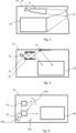
- a waveguide display element comprising a planar waveguide 10 comprising two opposing main surfaces extending essentially in a first plane.
- the waveguide is curved, the main surfaces however being mutually parallel at each lateral location.
- the reflector surface is arranged on the outer edge of the waveguide 10, as shown in Fig. 1A .
- the plane of the edge is perpendicular to the plane of the main surfaces of the waveguide 10.
- the edge reflector surface is a curved surface 14A when inspected in the plane of the main surfaces of the waveguide.
- the tangent of the curved surface 14A remains within the waveguide.
- a curved surface may be e.g. circular, elliptic or parabolic, or any other suitable shape, depending on the required optical function.
- the edge reflector surface 12A, 14A is capable of reflecting adapted to reflect light rays propagating within the waveguide between said main surfaces via total internal reflections, as visualized by the dashed arrows.
- the reflector surface 12B is located on an inner edge surface, i.e. surface of a void within the waveguide. This way, located within the waveguide at a distance from said outer edge surface, the reflector surface may be used to perform optical functions inside the waveguide. Positioning of the reflector surface is therefore very flexible.
- the reflector surface is arranged at a distance from outer (and optional inner) edge surfaces as an embedded optical surface 14B. That is there does not necessarily need to be a void inside the waveguide although this may simplify manufacturing.
- the inner edge reflector surface 12B is a straight surface and the embedded reflector surface 14B a curved surface, by way of example only. Any combination of placements/production methods and shapes is possible.
- the reflector surface comprises a grating, whose grating plane is parallel to the reflector surface.
- the grating vector of the grating is typically parallel to the plane of the main surfaces.
- One-dimensionally grated gratings are typical, although two-dimensional gratings capable of performing a more complex function are not excluded.
- the reflector surface comprises a reflective layer, such as a metal layer.
- the layer can be produced as a coating layer on an outer or inner edge, or embedded into the waveguide by some other technique known per se.
- the reflector surface comprises a thin-film stack of at least two different materials having different indices of refraction.
- a thin-film stack and a reflective coating layer applied on top of the thin-film stack.
- the stack may serve for example as an absorbing filter for a predefined wavelength range and angle of incidence, or an element capable of inducing phase shifts in a controlled manner.
- the waveguide comprises at least two separate grating areas typically arranged on at least one of the main surfaces thereof and the reflector surface is adapted to redirect light rays propagating between the grating areas.
- the waveguide comprises an exit pupil expander grating area and an out-coupling grating area, and there are one or more reflector surfaces arranged optically between the exit pupil expander grating area and the out-coupling grating area.
- the reflector surface is adapted to carry out a field-of-view compression or decompression optical function for a set of light rays representing an image coupled into the waveguide.
- the waveguide 10 comprises an in-coupling grating 21 adapted to couple light from the outside of the waveguide 10 into the waveguide as propagating light.
- the light is directed from the in-coupling grating 21 to an exit pupil expander (EPE) grating 22, which expands the light field in at least one, typically two lateral dimensions.
- EPE exit pupil expander
- From the EPE grating 22, the light is directed to a curved reflector surface 23.
- the surface 23 forms a convex mirror, which redirects the incoming light rays towards an out-coupling grating 24 (or a further EPE), at the same time decompressing the light field.
- the compression of the light field can be carried out using a concave reflector surface.
- the waveguide comprises an in-coupling grating area and an out-coupling grating area
- the reflector surface is arranged optically between the in-coupling grating area and the out-coupling grating area.
- Fig. 3 shows an example of such arrangement not according to the claimed invention.
- the waveguide 10 comprises an in-coupling grating 31 adapted to couple light from the outside of the waveguide 10 into the waveguide as propagating light. The light is directed from the in-coupling grating 31 to an opposing pair of reflector surfaces 33, 34, which expand the light field before directed to an out-coupling grating 38.
- An additional reflector surface 32 may be provided on the side of the element to prevent escaping of light rays bounced away from the out-coupling grating 38.
- the waveguide comprises an attached or integrated image source arrangement and at least one diffractive grating
- the reflector surface is adapted to redirect light rays propagating within the light image source arrangement and/or between the image source arrangement and the diffractive grating.
- the image source arrangement may comprise a light source element integral with the waveguide and a display panel integral with the waveguide, wherein the reflector surface is adapted to redirect light rays propagating between the light source element and the display panel.
- the waveguide element can be used in a personal see-through display device, such as a head-mounted display device, like a near-to-the-eye device or head-up display device.
Landscapes
- Physics & Mathematics (AREA)
- General Physics & Mathematics (AREA)
- Optics & Photonics (AREA)
- Diffracting Gratings Or Hologram Optical Elements (AREA)
- Optical Couplings Of Light Guides (AREA)
- Optical Elements Other Than Lenses (AREA)
Applications Claiming Priority (2)
| Application Number | Priority Date | Filing Date | Title |
|---|---|---|---|
| FI20185293A FI128552B (en) | 2018-03-28 | 2018-03-28 | Waveguide display element with reflector surface |
| PCT/FI2019/050190 WO2019185978A1 (en) | 2018-03-28 | 2019-03-11 | Waveguide display element with reflector surface |
Publications (4)
| Publication Number | Publication Date |
|---|---|
| EP3729179A1 EP3729179A1 (en) | 2020-10-28 |
| EP3729179A4 EP3729179A4 (en) | 2021-09-08 |
| EP3729179C0 EP3729179C0 (en) | 2025-05-07 |
| EP3729179B1 true EP3729179B1 (en) | 2025-05-07 |
Family
ID=68061018
Family Applications (1)
| Application Number | Title | Priority Date | Filing Date |
|---|---|---|---|
| EP19776864.1A Active EP3729179B1 (en) | 2018-03-28 | 2019-03-11 | Waveguide element for a display with reflector surface |
Country Status (8)
| Country | Link |
|---|---|
| US (1) | US11067812B2 (https=) |
| EP (1) | EP3729179B1 (https=) |
| JP (1) | JP7394064B2 (https=) |
| KR (1) | KR102743739B1 (https=) |
| CN (1) | CN111936911A (https=) |
| FI (1) | FI128552B (https=) |
| SG (1) | SG11202008140PA (https=) |
| WO (1) | WO2019185978A1 (https=) |
Families Citing this family (2)
| Publication number | Priority date | Publication date | Assignee | Title |
|---|---|---|---|---|
| DE102021213913A1 (de) | 2021-12-07 | 2023-06-07 | Blue Wonder Vermögensverwaltungs GmbH | Vorrichtung und Verfahren zum Darstellen von Informationen für einen Nutzer |
| CN118091822A (zh) * | 2022-02-16 | 2024-05-28 | 荣耀终端有限公司 | 一种显示设备、光波导和增强现实眼镜 |
Family Cites Families (17)
| Publication number | Priority date | Publication date | Assignee | Title |
|---|---|---|---|---|
| JPS6090311A (ja) * | 1983-10-24 | 1985-05-21 | Nippon Telegr & Teleph Corp <Ntt> | 回折格子付光導波膜の製造方法 |
| US5890796A (en) * | 1997-01-16 | 1999-04-06 | Ford Global Technologies, Inc. | Laser illuminated lighting system utilizing a diffractive optical element |
| US7133207B2 (en) * | 2004-02-18 | 2006-11-07 | Icuiti Corporation | Micro-display engine |
| JP4308712B2 (ja) * | 2004-05-31 | 2009-08-05 | 富士通株式会社 | 光デバイス |
| EP2241926A1 (en) | 2009-04-14 | 2010-10-20 | BAE Systems PLC | Optical waveguide and display device |
| US9523852B1 (en) * | 2012-03-28 | 2016-12-20 | Rockwell Collins, Inc. | Micro collimator system and method for a head up display (HUD) |
| EP2850471B1 (en) * | 2012-05-18 | 2020-08-26 | RealD Spark, LLC | Directionally illuminated waveguide arrangement |
| US8915635B2 (en) * | 2013-03-13 | 2014-12-23 | Hewlett-Packard Development Company, L.P. | Backlight having dual collimating reflectors |
| KR102651578B1 (ko) * | 2013-11-27 | 2024-03-25 | 매직 립, 인코포레이티드 | 가상 및 증강 현실 시스템들 및 방법들 |
| US9474902B2 (en) * | 2013-12-31 | 2016-10-25 | Nano Retina Ltd. | Wearable apparatus for delivery of power to a retinal prosthesis |
| EP3198192A1 (en) * | 2014-09-26 | 2017-08-02 | Milan Momcilo Popovich | Holographic waveguide opticaltracker |
| US9632226B2 (en) * | 2015-02-12 | 2017-04-25 | Digilens Inc. | Waveguide grating device |
| JP6720315B2 (ja) * | 2016-01-06 | 2020-07-08 | ビュージックス コーポレーションVuzix Corporation | 反射型転換アレイを有する結像光ガイド |
| CN205787362U (zh) * | 2016-02-26 | 2016-12-07 | 中国航空工业集团公司洛阳电光设备研究所 | 光波导元件、二维扩展光波导器件、平视显示装置及照明装置 |
| CN107229118A (zh) * | 2016-03-23 | 2017-10-03 | 北京亮亮视野科技有限公司 | 头戴式可视设备hmd波导光学系统 |
| CN106125194B (zh) * | 2016-09-06 | 2018-11-06 | 北京耐德佳显示技术有限公司 | 波导型元件及使用其的头戴式显示装置 |
| DE102017130344A1 (de) * | 2017-12-18 | 2019-06-19 | Carl Zeiss Ag | Optisches System zum Übertragen eines Quellbildes |
-
2018
- 2018-03-28 FI FI20185293A patent/FI128552B/en active IP Right Grant
-
2019
- 2019-03-11 CN CN201980021742.3A patent/CN111936911A/zh active Pending
- 2019-03-11 JP JP2020545642A patent/JP7394064B2/ja active Active
- 2019-03-11 SG SG11202008140PA patent/SG11202008140PA/en unknown
- 2019-03-11 KR KR1020207023662A patent/KR102743739B1/ko active Active
- 2019-03-11 US US17/041,301 patent/US11067812B2/en active Active
- 2019-03-11 WO PCT/FI2019/050190 patent/WO2019185978A1/en not_active Ceased
- 2019-03-11 EP EP19776864.1A patent/EP3729179B1/en active Active
Also Published As
| Publication number | Publication date |
|---|---|
| CN111936911A (zh) | 2020-11-13 |
| SG11202008140PA (en) | 2020-09-29 |
| US20210055562A1 (en) | 2021-02-25 |
| EP3729179A1 (en) | 2020-10-28 |
| JP7394064B2 (ja) | 2023-12-07 |
| WO2019185978A1 (en) | 2019-10-03 |
| FI128552B (en) | 2020-07-31 |
| JP2021516778A (ja) | 2021-07-08 |
| KR102743739B1 (ko) | 2024-12-17 |
| EP3729179C0 (en) | 2025-05-07 |
| US11067812B2 (en) | 2021-07-20 |
| FI20185293A1 (en) | 2019-09-29 |
| KR20200136370A (ko) | 2020-12-07 |
| EP3729179A4 (en) | 2021-09-08 |
| CA3087651A1 (en) | 2019-10-03 |
Similar Documents
| Publication | Publication Date | Title |
|---|---|---|
| EP3914955B1 (en) | Novel grating arrangements | |
| EP3710883B1 (en) | Diffractive waveguide element and diffractive waveguide display | |
| CA2758633C (en) | Optical waveguide and display device | |
| EP3732528B1 (en) | Exit pupil expander | |
| EP2241926A1 (en) | Optical waveguide and display device | |
| EP3729179B1 (en) | Waveguide element for a display with reflector surface | |
| CA3087651C (en) | Waveguide display element with reflector surface | |
| EP3729181B1 (en) | Diffractive exit pupil expander arrangement for display applications | |
| JP2021516778A5 (https=) |
Legal Events
| Date | Code | Title | Description |
|---|---|---|---|
| STAA | Information on the status of an ep patent application or granted ep patent |
Free format text: STATUS: THE INTERNATIONAL PUBLICATION HAS BEEN MADE |
|
| PUAI | Public reference made under article 153(3) epc to a published international application that has entered the european phase |
Free format text: ORIGINAL CODE: 0009012 |
|
| STAA | Information on the status of an ep patent application or granted ep patent |
Free format text: STATUS: REQUEST FOR EXAMINATION WAS MADE |
|
| 17P | Request for examination filed |
Effective date: 20200724 |
|
| AK | Designated contracting states |
Kind code of ref document: A1 Designated state(s): AL AT BE BG CH CY CZ DE DK EE ES FI FR GB GR HR HU IE IS IT LI LT LU LV MC MK MT NL NO PL PT RO RS SE SI SK SM TR |
|
| AX | Request for extension of the european patent |
Extension state: BA ME |
|
| DAV | Request for validation of the european patent (deleted) | ||
| DAX | Request for extension of the european patent (deleted) | ||
| A4 | Supplementary search report drawn up and despatched |
Effective date: 20210809 |
|
| RIC1 | Information provided on ipc code assigned before grant |
Ipc: G02B 5/18 20060101ALI20210803BHEP Ipc: G02B 27/00 20060101ALI20210803BHEP Ipc: G02B 27/42 20060101ALI20210803BHEP Ipc: G02B 27/09 20060101ALI20210803BHEP Ipc: G02B 27/01 20060101AFI20210803BHEP |
|
| STAA | Information on the status of an ep patent application or granted ep patent |
Free format text: STATUS: EXAMINATION IS IN PROGRESS |
|
| 17Q | First examination report despatched |
Effective date: 20230504 |
|
| GRAP | Despatch of communication of intention to grant a patent |
Free format text: ORIGINAL CODE: EPIDOSNIGR1 |
|
| STAA | Information on the status of an ep patent application or granted ep patent |
Free format text: STATUS: GRANT OF PATENT IS INTENDED |
|
| INTG | Intention to grant announced |
Effective date: 20250124 |
|
| GRAS | Grant fee paid |
Free format text: ORIGINAL CODE: EPIDOSNIGR3 |
|
| GRAA | (expected) grant |
Free format text: ORIGINAL CODE: 0009210 |
|
| STAA | Information on the status of an ep patent application or granted ep patent |
Free format text: STATUS: THE PATENT HAS BEEN GRANTED |
|
| AK | Designated contracting states |
Kind code of ref document: B1 Designated state(s): AL AT BE BG CH CY CZ DE DK EE ES FI FR GB GR HR HU IE IS IT LI LT LU LV MC MK MT NL NO PL PT RO RS SE SI SK SM TR |
|
| REG | Reference to a national code |
Ref country code: GB Ref legal event code: FG4D |
|
| REG | Reference to a national code |
Ref country code: CH Ref legal event code: EP |
|
| REG | Reference to a national code |
Ref country code: IE Ref legal event code: FG4D |
|
| U01 | Request for unitary effect filed |
Effective date: 20250512 |
|
| U07 | Unitary effect registered |
Designated state(s): AT BE BG DE DK EE FI FR IT LT LU LV MT NL PT RO SE SI Effective date: 20250516 |
|
| PG25 | Lapsed in a contracting state [announced via postgrant information from national office to epo] |
Ref country code: ES Free format text: LAPSE BECAUSE OF FAILURE TO SUBMIT A TRANSLATION OF THE DESCRIPTION OR TO PAY THE FEE WITHIN THE PRESCRIBED TIME-LIMIT Effective date: 20250507 |
|
| PG25 | Lapsed in a contracting state [announced via postgrant information from national office to epo] |
Ref country code: NO Free format text: LAPSE BECAUSE OF FAILURE TO SUBMIT A TRANSLATION OF THE DESCRIPTION OR TO PAY THE FEE WITHIN THE PRESCRIBED TIME-LIMIT Effective date: 20250807 Ref country code: GR Free format text: LAPSE BECAUSE OF FAILURE TO SUBMIT A TRANSLATION OF THE DESCRIPTION OR TO PAY THE FEE WITHIN THE PRESCRIBED TIME-LIMIT Effective date: 20250808 |
|
| PG25 | Lapsed in a contracting state [announced via postgrant information from national office to epo] |
Ref country code: PL Free format text: LAPSE BECAUSE OF FAILURE TO SUBMIT A TRANSLATION OF THE DESCRIPTION OR TO PAY THE FEE WITHIN THE PRESCRIBED TIME-LIMIT Effective date: 20250507 |
|
| PG25 | Lapsed in a contracting state [announced via postgrant information from national office to epo] |
Ref country code: HR Free format text: LAPSE BECAUSE OF FAILURE TO SUBMIT A TRANSLATION OF THE DESCRIPTION OR TO PAY THE FEE WITHIN THE PRESCRIBED TIME-LIMIT Effective date: 20250507 |
|
| PG25 | Lapsed in a contracting state [announced via postgrant information from national office to epo] |
Ref country code: RS Free format text: LAPSE BECAUSE OF FAILURE TO SUBMIT A TRANSLATION OF THE DESCRIPTION OR TO PAY THE FEE WITHIN THE PRESCRIBED TIME-LIMIT Effective date: 20250807 |
|
| PG25 | Lapsed in a contracting state [announced via postgrant information from national office to epo] |
Ref country code: IS Free format text: LAPSE BECAUSE OF FAILURE TO SUBMIT A TRANSLATION OF THE DESCRIPTION OR TO PAY THE FEE WITHIN THE PRESCRIBED TIME-LIMIT Effective date: 20250907 |
|
| PG25 | Lapsed in a contracting state [announced via postgrant information from national office to epo] |
Ref country code: SM Free format text: LAPSE BECAUSE OF FAILURE TO SUBMIT A TRANSLATION OF THE DESCRIPTION OR TO PAY THE FEE WITHIN THE PRESCRIBED TIME-LIMIT Effective date: 20250507 |
|
| PG25 | Lapsed in a contracting state [announced via postgrant information from national office to epo] |
Ref country code: CZ Free format text: LAPSE BECAUSE OF FAILURE TO SUBMIT A TRANSLATION OF THE DESCRIPTION OR TO PAY THE FEE WITHIN THE PRESCRIBED TIME-LIMIT Effective date: 20250507 |
|
| PG25 | Lapsed in a contracting state [announced via postgrant information from national office to epo] |
Ref country code: SK Free format text: LAPSE BECAUSE OF FAILURE TO SUBMIT A TRANSLATION OF THE DESCRIPTION OR TO PAY THE FEE WITHIN THE PRESCRIBED TIME-LIMIT Effective date: 20250507 |
|
| PLBE | No opposition filed within time limit |
Free format text: ORIGINAL CODE: 0009261 |
|
| STAA | Information on the status of an ep patent application or granted ep patent |
Free format text: STATUS: NO OPPOSITION FILED WITHIN TIME LIMIT |
|
| REG | Reference to a national code |
Ref country code: CH Ref legal event code: L10 Free format text: ST27 STATUS EVENT CODE: U-0-0-L10-L00 (AS PROVIDED BY THE NATIONAL OFFICE) Effective date: 20260318 |
|
| PGFP | Annual fee paid to national office [announced via postgrant information from national office to epo] |
Ref country code: GB Payment date: 20260327 Year of fee payment: 8 |
|
| 26N | No opposition filed |
Effective date: 20260210 |