EP3710883B1 - Diffractive waveguide element and diffractive waveguide display - Google Patents
Diffractive waveguide element and diffractive waveguide display Download PDFInfo
- Publication number
- EP3710883B1 EP3710883B1 EP18891531.8A EP18891531A EP3710883B1 EP 3710883 B1 EP3710883 B1 EP 3710883B1 EP 18891531 A EP18891531 A EP 18891531A EP 3710883 B1 EP3710883 B1 EP 3710883B1
- Authority
- EP
- European Patent Office
- Prior art keywords
- waveguide
- ray
- display
- rays
- diffractive optical
- Prior art date
- Legal status (The legal status is an assumption and is not a legal conclusion. Google has not performed a legal analysis and makes no representation as to the accuracy of the status listed.)
- Active
Links
- 238000010168 coupling process Methods 0.000 claims description 50
- 238000005859 coupling reaction Methods 0.000 claims description 50
- 230000003287 optical effect Effects 0.000 claims description 29
- 230000001902 propagating effect Effects 0.000 claims description 6
- 230000008878 coupling Effects 0.000 claims description 5
- 238000011144 upstream manufacturing Methods 0.000 claims description 5
- 210000001747 pupil Anatomy 0.000 description 22
- 241000218228 Humulus Species 0.000 description 10
- 230000000694 effects Effects 0.000 description 4
- 230000008901 benefit Effects 0.000 description 3
- 238000006073 displacement reaction Methods 0.000 description 3
- 230000003190 augmentative effect Effects 0.000 description 2
- 244000025221 Humulus lupulus Species 0.000 description 1
- 230000015572 biosynthetic process Effects 0.000 description 1
- 230000003247 decreasing effect Effects 0.000 description 1
- 238000000280 densification Methods 0.000 description 1
- 230000001419 dependent effect Effects 0.000 description 1
- 230000000737 periodic effect Effects 0.000 description 1
- 239000013598 vector Substances 0.000 description 1
Images

Classifications
-
- G—PHYSICS
- G02—OPTICS
- G02B—OPTICAL ELEMENTS, SYSTEMS OR APPARATUS
- G02B27/00—Optical systems or apparatus not provided for by any of the groups G02B1/00 - G02B26/00, G02B30/00
- G02B27/42—Diffraction optics, i.e. systems including a diffractive element being designed for providing a diffractive effect
- G02B27/4272—Diffraction optics, i.e. systems including a diffractive element being designed for providing a diffractive effect having plural diffractive elements positioned sequentially along the optical path
-
- G—PHYSICS
- G02—OPTICS
- G02B—OPTICAL ELEMENTS, SYSTEMS OR APPARATUS
- G02B27/00—Optical systems or apparatus not provided for by any of the groups G02B1/00 - G02B26/00, G02B30/00
- G02B27/01—Head-up displays
-
- G—PHYSICS
- G02—OPTICS
- G02B—OPTICAL ELEMENTS, SYSTEMS OR APPARATUS
- G02B27/00—Optical systems or apparatus not provided for by any of the groups G02B1/00 - G02B26/00, G02B30/00
-
- G—PHYSICS
- G02—OPTICS
- G02B—OPTICAL ELEMENTS, SYSTEMS OR APPARATUS
- G02B27/00—Optical systems or apparatus not provided for by any of the groups G02B1/00 - G02B26/00, G02B30/00
- G02B27/0081—Optical systems or apparatus not provided for by any of the groups G02B1/00 - G02B26/00, G02B30/00 with means for altering, e.g. enlarging, the entrance or exit pupil
-
- G—PHYSICS
- G02—OPTICS
- G02B—OPTICAL ELEMENTS, SYSTEMS OR APPARATUS
- G02B27/00—Optical systems or apparatus not provided for by any of the groups G02B1/00 - G02B26/00, G02B30/00
- G02B27/01—Head-up displays
- G02B27/0101—Head-up displays characterised by optical features
-
- G—PHYSICS
- G02—OPTICS
- G02B—OPTICAL ELEMENTS, SYSTEMS OR APPARATUS
- G02B27/00—Optical systems or apparatus not provided for by any of the groups G02B1/00 - G02B26/00, G02B30/00
- G02B27/01—Head-up displays
- G02B27/0101—Head-up displays characterised by optical features
- G02B27/0103—Head-up displays characterised by optical features comprising holographic elements
-
- G—PHYSICS
- G02—OPTICS
- G02B—OPTICAL ELEMENTS, SYSTEMS OR APPARATUS
- G02B27/00—Optical systems or apparatus not provided for by any of the groups G02B1/00 - G02B26/00, G02B30/00
- G02B27/01—Head-up displays
- G02B27/017—Head mounted
-
- G—PHYSICS
- G02—OPTICS
- G02B—OPTICAL ELEMENTS, SYSTEMS OR APPARATUS
- G02B27/00—Optical systems or apparatus not provided for by any of the groups G02B1/00 - G02B26/00, G02B30/00
- G02B27/01—Head-up displays
- G02B27/017—Head mounted
- G02B27/0172—Head mounted characterised by optical features
-
- G—PHYSICS
- G02—OPTICS
- G02B—OPTICAL ELEMENTS, SYSTEMS OR APPARATUS
- G02B5/00—Optical elements other than lenses
-
- G—PHYSICS
- G02—OPTICS
- G02B—OPTICAL ELEMENTS, SYSTEMS OR APPARATUS
- G02B5/00—Optical elements other than lenses
- G02B5/18—Diffraction gratings
- G02B5/1814—Diffraction gratings structurally combined with one or more further optical elements, e.g. lenses, mirrors, prisms or other diffraction gratings
-
- G—PHYSICS
- G02—OPTICS
- G02B—OPTICAL ELEMENTS, SYSTEMS OR APPARATUS
- G02B5/00—Optical elements other than lenses
- G02B5/18—Diffraction gratings
- G02B5/1828—Diffraction gratings having means for producing variable diffraction
-
- G—PHYSICS
- G02—OPTICS
- G02B—OPTICAL ELEMENTS, SYSTEMS OR APPARATUS
- G02B6/00—Light guides; Structural details of arrangements comprising light guides and other optical elements, e.g. couplings
-
- G—PHYSICS
- G02—OPTICS
- G02B—OPTICAL ELEMENTS, SYSTEMS OR APPARATUS
- G02B6/00—Light guides; Structural details of arrangements comprising light guides and other optical elements, e.g. couplings
- G02B6/10—Light guides; Structural details of arrangements comprising light guides and other optical elements, e.g. couplings of the optical waveguide type
-
- G—PHYSICS
- G02—OPTICS
- G02B—OPTICAL ELEMENTS, SYSTEMS OR APPARATUS
- G02B6/00—Light guides; Structural details of arrangements comprising light guides and other optical elements, e.g. couplings
- G02B6/0001—Light guides; Structural details of arrangements comprising light guides and other optical elements, e.g. couplings specially adapted for lighting devices or systems
- G02B6/0011—Light guides; Structural details of arrangements comprising light guides and other optical elements, e.g. couplings specially adapted for lighting devices or systems the light guides being planar or of plate-like form
- G02B6/0013—Means for improving the coupling-in of light from the light source into the light guide
- G02B6/0015—Means for improving the coupling-in of light from the light source into the light guide provided on the surface of the light guide or in the bulk of it
- G02B6/0016—Grooves, prisms, gratings, scattering particles or rough surfaces
-
- G—PHYSICS
- G02—OPTICS
- G02B—OPTICAL ELEMENTS, SYSTEMS OR APPARATUS
- G02B6/00—Light guides; Structural details of arrangements comprising light guides and other optical elements, e.g. couplings
- G02B6/0001—Light guides; Structural details of arrangements comprising light guides and other optical elements, e.g. couplings specially adapted for lighting devices or systems
- G02B6/0011—Light guides; Structural details of arrangements comprising light guides and other optical elements, e.g. couplings specially adapted for lighting devices or systems the light guides being planar or of plate-like form
- G02B6/0013—Means for improving the coupling-in of light from the light source into the light guide
- G02B6/0023—Means for improving the coupling-in of light from the light source into the light guide provided by one optical element, or plurality thereof, placed between the light guide and the light source, or around the light source
- G02B6/0028—Light guide, e.g. taper
-
- G—PHYSICS
- G02—OPTICS
- G02B—OPTICAL ELEMENTS, SYSTEMS OR APPARATUS
- G02B6/00—Light guides; Structural details of arrangements comprising light guides and other optical elements, e.g. couplings
- G02B6/0001—Light guides; Structural details of arrangements comprising light guides and other optical elements, e.g. couplings specially adapted for lighting devices or systems
- G02B6/0011—Light guides; Structural details of arrangements comprising light guides and other optical elements, e.g. couplings specially adapted for lighting devices or systems the light guides being planar or of plate-like form
- G02B6/0033—Means for improving the coupling-out of light from the light guide
- G02B6/0035—Means for improving the coupling-out of light from the light guide provided on the surface of the light guide or in the bulk of it
- G02B6/004—Scattering dots or dot-like elements, e.g. microbeads, scattering particles, nanoparticles
- G02B6/0043—Scattering dots or dot-like elements, e.g. microbeads, scattering particles, nanoparticles provided on the surface of the light guide
Definitions
- the invention relates to diffractive waveguides.
- Such waveguides can be used in personal display devices, such as head-mounted displays (HMDs) and head-up displays (HUDs).
- HMDs head-mounted displays
- HUDs head-up displays
- Waveguides are key image-forming elements in many modern personal display devices.
- the image to be displayed can be coupled into and out of the waveguide, as well as modified within the waveguide, using diffractive gratings.
- diffractive gratings there may be provided an in-coupling grating for coupling an image from a projector into the waveguide, an exit pupil expander grating for expanding the light field in one or more in-plane dimensions of the waveguide, and an out-coupling grating which couples the image of the waveguide to the user's eye.
- the invention is based on the idea of providing, in connection with an in-coupling diffractive optical element of a waveguide, a ray multiplier element that is capable of splitting incoming rays into a plurality of parallel rays that propagate in the waveguide displaced from each other.
- the multiplier can be designed such at least one ray, preferably a plurality of rays, exit to the pupil of the viewer, at all angles of incidence, whereby striping is prevented.
- the ray multiplier element can be adapted to split the incoming ray in one or two dimensions.
- the invention provides a diffractive waveguide element for a personal display device, the element comprising a display waveguide extending in a waveguide plane, an in-coupling diffractive optical element arranged onto or into the display waveguide for diffractively coupling light rays into the display waveguide, and an out-coupling diffractive optical element arranged onto or into the display waveguide for coupling the diffractively coupled light rays out of the display waveguide.
- a ray multiplier element optically upstream of the out-coupling diffractive optical element, the ray multiplier element being capable of splitting a light ray incoming to the in-coupling grating into a plurality of parallel rays spatially displaced in the waveguide plane before they enter the out-coupling diffractive optical element.
- the ray multiplier element may be provided either upstream or downstream of the in-coupling diffractive optical element.
- the density of the plurality of parallel rays i.e. including the original ray and multiplied rays, is higher than the hop length of the incoming light ray in the direction of propagation of the incoming light ray in the display waveguide. This ensures that real ray densification of the light field take place.
- the invention provides a diffractive waveguide display comprising a diffractive waveguide element of the above kind, and an image projector adapted to project a plurality of laser rays onto said in-coupling diffractive optical element, the rays being spatially multiplied in the ray multiplier element.
- the initial single beam emitted by the image projector exits as a parallel multi-ray beam from the out-coupling grating.
- the spatial displacement of multiplied rays at each particular angle that takes place in the ray multiplier element is different from the hop length of the rays in the display waveguide, so that additional spatial spreading of the rays takes place.
- the displacement is smaller than the hop length in the waveguide.
- the invention offers significant benefits.
- the ray multiplier increases the bouncing density of rays propagating in the waveguide and therefore increases the number of out-coupled rays per unit area at the out-coupling grating. This increases the probability or fully ensures that there is at least one ray that exits to the eye pupil of the viewer. Thus, striping is prevented or at least decreased and an integral and more homogeneous (stripe-free) image is seen.
- the invention improves the performance of the display in particular with high angles of incidence, which have previously been prone to striping.
- the invention differs from conventional exit pupil expander (EPE) gratings such that the density of the plurality of parallel rays is higher than the hop length in the direction of propagation of the incoming light.
- EPEs according to prior art are incapable of densifying the light field in the original propagation direction, but only in the transverse direction.
- the invention can be implemented with relatively simple ray multiplier element with minor or no changes the overall waveguide design. No changes are required in the projector.
- the ray multiplier element comprises a planar multiplier waveguide having a thickness smaller than said display waveguide.
- the multiplier waveguide can be positioned such that it directly interacts with the in-coupling diffractive optical element so as to cause the ray multiplication in at least one dimension. Additional grating or micromirror arrangement, for example, can be provided to cause multiplication in the other dimension.
- the multiplier waveguide is arranged onto or below the surface of the display waveguide aligned with the in-coupling diffractive optical element. Thus, the multiplication can be achieved without increasing the footprint of the waveguide.
- the ray multiplier element comprises one or more micromirror elements or diffractive gratings adapted to carry out or facilitate the splitting of the incoming light ray.
- the multiplier element is a zone in the display waveguide having two diffractive gratings arranged on opposite surfaces of the display waveguide and on the propagating path of the light diffracted into the waveguide by said in-coupling diffractive optical element.
- the diffractive gratings, or more generally diffractive optical elements, cause the required displacement for rays hitting them.
- the ray multiplier element is configured to split the light ray only above predefined angle of incidence of the incoming ray.
- the ray multiplier element can be configured to provide at least two different multiplication factors for at least two different angles of incidence of the incoming rays, respectively.
- the waveguide element is a laser-illuminated element, in which each single ray at having a specific angle of incidence corresponds to a single pixel of the image seen by the user.
- the image projector is a laser beam projector, such as a scanning beam projector.
- Diffractive optical element herein refers to gratings and other optical structures that contain regular or non-regular features having at least one dimension in the order of visible light wavelengths, i.e, typically less than 1 ⁇ m, and thus causes significant diffraction of light. Examples include line gratings (one dimensional gratings) and two-dimensional gratings.
- the gratings can be single-region gratings (with the same microstructure and optical response throughout the grating area) or multi-region gratings (i.e. containing zones having different microstructures and optical responses).
- Hop length is the distance between two successive bouncing points of light propagating in a waveguide via total internal reflections on the same surface of the waveguide.
- Beam multipliers herein discussed are needed for example when augmented reality (AR) waveguides are illuminated by laser light.
- AR augmented reality
- the pupil of the human eye has a diameter exceeding 2 mm, which means that the beams should be separated by no more than this distance from each other at the out-coupling region to ensure an uninterrupted image in all situations.
- the inter-beam distances after exit pupil expansion may be as large as 5 mm, and thus the beams must be subdivided additionally (to the EPE function). This additional subdivision is the purpose of the present ray multiplier.
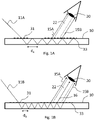
- Fig. 1A shows a planar waveguide 10 having an in-coupling grating 31 and an out-coupling grating 33.
- incident ray 11A is diffracted by the in-coupling grating 31 into the waveguide 10, where it propagates via total internal reflections.
- the angle of incidence of the incoming ray 11A is relatively high with respect to the normal of the waveguide, whereby also the diffraction angle is high and hop length (bouncing period) d A is long. Because of the long period, the rays 15A, 15B exiting the waveguide at the region of the out-coupling grating 33 miss the pupil 20 of the viewer's eye. In order for a ray at a specific angle to be seen, it should exit within the zone of sight 22 for that angle.
- Fig. 1B shows a modified situation, where the angle of incidence of the incoming ray 11B is lower, making also the diffraction angle lower and hop length d B shorter. Now, one exiting ray 16 meets the pupil 20. Even if the eye is moved, at least one of the exiting rays 15A, 16, 15B will always meet the pupil 20.
- the present beam multiplier element may be a component separate from the main waveguide of the display element or it may be integrated as part of the waveguide functionality. It can be realized using a combination of gratings and/or controlling the waveguide thickness. Non-limiting examples are discussed below.
- the beam multiplier element is provided upstream of the in-coupling grating taking advantage of an additional waveguide having a thickness smaller than the thickness of the main display waveguide.
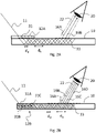
- Fig. 2A shows an embodiment, where a ray multiplier element 12A is provided on the waveguide 10.
- the element 12A herein comprises a multiplier waveguide which is thinner and smaller in area than the main waveguide 10.
- the in-coupling grating is located downstream of the multiplier element between the multiplier waveguide and the display waveguide 10.
- the incident ray 11 bounces inside the multiplier waveguide with a short bounce period, and at every bounce at the in-coupling grating 31, part of the light is diffracted into the display waveguide 10.
- the ray is multiplied and at least one, herein two, rays 16A, 16B exit to the eye pupil 20.
- Fig. 2B shows an embodiment, where the ray multiplier element 12B is formed by two thin multiplication/multiplier waveguides 31A, 31B and an intermediate DOE 31C therebetween.
- the thin portions interact so that the amount of rays is multiplied when they escape into the main waveguide 10 for propagation therein towards the out-coupling grating 33.
- four rays 16A-D hit the pupil 20 of the eye.
- light propagates in the stacked thin layers into different directions, which also provides an efficient beam multiplier configuration.
- Fig. 2C shows an embodiment, where the ray multiplier element 12C comprises two multiplier gratings 14A, 14B arranged on opposite surfaces of the display waveguide 10.
- the gratings are adapted to diffract the rays into lower angle, again with the result that one or more beams 16A, 16B exit to the eye pupil 20.
- the initial in-coupled ray hits the first multiplier grating 14A on a first side (here the bottom side) of the waveguide 10
- a first part of it continues "normally” via total internal reflection and second part of it is directed by reflective diffraction towards the second multiplier grating 14A on the second side (here the upper side) of the waveguide 10.
- the second ray is again reflectively diffracted and continues in the same propagation angle as the first ray but displaced therefrom.
- both rays "fit" into the eye pupil pipe of sight 22.
- the multiplier gratings 14A, 14B are similar to each other, i.e., have the same grating periods and orientations (or more generally grating vectors).
- the multiplication factor is two, but by extending the width of the ray multiplier element 12C, i.e. the multiplier gratings 14A, 14B therein, a multiplication factor of more than two can be achieved.
- the multiplier gratings 14A, 14B are replaced with some optical element carrying out essentially the same optical function.
- the same angle-maintaining beam-splitting effect can be achieved.
- the multiplier element is provided as a thin waveguide layer on top the thicker main waveguide layer at the region of the out-coupling grating. As light leaks from the main waveguide into the thin waveguide, its hop length shortens. The shorter hop length shortens the distance of exiting rays that are coupled out by the out-coupling grating/DOE that sits on top of the thin layer.
- the multiplier element is capable of providing a multiplication factor of at least 4, in particular at least 9, such as 4 - 100, for high incident angle beams, that is, beams at the FOV limit angles of the display element.
- the multiplication element may be configured to provide at least 9 beams per pupil area having a diameter of 2 mm for all angles within the FOV of the display device.
- Fig. 3 illustrates the invention as a top view of the waveguide 10.
- the ray multiplier element 12 is aligned with the in-coupling grating 31 in order to replicate the original beam 11 into additional beams 11' displaced in two dimensions and propagating into the same direction.
- the beams 11, 11' travel to an exit pupil expander (EPE) grating 32, to increase the exit pupil in one or two dimensions.
- EPE exit pupil expander
- the rays continue towards the out-coupling grating 33, from which the out-coupled beams 16, 16', corresponding to the original and replicated beams 11, 11' and extended across the whole out-coupling grating 33, exit parallel to each other.
- EPE exit pupil expander
- the dashed circles 19 illustrate the original pupil size, i.e. herein the area of the in-coupling grating 31, which is replicated several times on the out-coupling grating 33.
- the illustrated multiplication factor is 2x2, i.e., 4, but other symmetric or non-symmetric multiplication factors can be implemented as well, as understood from the above-described examples.
- the illustrated examples show the ray-multiplication effect for one angle of incidence only.
- the same effect is, however, seen at a wider range of angles that meet the in-coupling grating and the ray multiplier element.
- the angle range can be controlled and even different multiplication factors provided for different angles.
- the multiplication factor for at least some high angles of incidence is configured to be higher than the multiplication factor for at least some low angles of incidence (for which the hop length is inherently shorter and the problem less relevant).
- Embodiments of the invention can be utilized in various personal display devices, augmented reality (AR), virtual reality (VR) and mixed reality (MR) devices, like near-to-the-eye displays (NEDs) and other head-mounted displays (HMDs), as well as head-up displays (HUDs), in their different forms.
- AR augmented reality
- VR virtual reality
- MR mixed reality
- NEDs near-to-the-eye displays
- HMDs head-mounted displays
- HUDs head-up displays
- the waveguide or individual layers thereof may comprise, in addition to the in-coupling, exit pupil expander and out-coupling gratings, also other diffractive optical elements, such as beam redirection gratings.
Description
- The invention relates to diffractive waveguides. Such waveguides can be used in personal display devices, such as head-mounted displays (HMDs) and head-up displays (HUDs).
- Waveguides are key image-forming elements in many modern personal display devices. The image to be displayed can be coupled into and out of the waveguide, as well as modified within the waveguide, using diffractive gratings. For example, there may be provided an in-coupling grating for coupling an image from a projector into the waveguide, an exit pupil expander grating for expanding the light field in one or more in-plane dimensions of the waveguide, and an out-coupling grating which couples the image of the waveguide to the user's eye.
- One problem related to diffractive waveguide elements is striping of the image out-coupled therefrom. This is because the light beams travelling in the waveguide via total internal reflections may have a bouncing period, i.e. hop length, longer than the diameter of the eye pupil of the viewer. In this case, a pixel may be diffracted beside the pupil and be therefore not visible for the user. This effect is noticeable in particular with high angles of incidence (with respect to the normal of the waveguide) and when laser projector is used for image formation, since each image pixel is composed of a narrow beam only. Documents
US 2016/291328 A1 ,WO 2017/207987 A1 , andUS 2017/131551 A1 disclose waveguide elements for image forming devices. - It is an aim of the invention to solve the abovementioned problem and to provide solution that prevents or diminishes striping and helps to provide a more integral image.
- The invention is based on the idea of providing, in connection with an in-coupling diffractive optical element of a waveguide, a ray multiplier element that is capable of splitting incoming rays into a plurality of parallel rays that propagate in the waveguide displaced from each other. The multiplier can be designed such at least one ray, preferably a plurality of rays, exit to the pupil of the viewer, at all angles of incidence, whereby striping is prevented. The ray multiplier element can be adapted to split the incoming ray in one or two dimensions.
- In particular, the invention is characterized by what is stated in the independent claims.
- According to a first aspect, the invention provides a diffractive waveguide element for a personal display device, the element comprising a display waveguide extending in a waveguide plane, an in-coupling diffractive optical element arranged onto or into the display waveguide for diffractively coupling light rays into the display waveguide, and an out-coupling diffractive optical element arranged onto or into the display waveguide for coupling the diffractively coupled light rays out of the display waveguide. In addition, there is provided a ray multiplier element optically upstream of the out-coupling diffractive optical element, the ray multiplier element being capable of splitting a light ray incoming to the in-coupling grating into a plurality of parallel rays spatially displaced in the waveguide plane before they enter the out-coupling diffractive optical element. The ray multiplier element may be provided either upstream or downstream of the in-coupling diffractive optical element.
- In particular, the density of the plurality of parallel rays, i.e. including the original ray and multiplied rays, is higher than the hop length of the incoming light ray in the direction of propagation of the incoming light ray in the display waveguide. This ensures that real ray densification of the light field take place.
- According to a second aspect, the invention provides a diffractive waveguide display comprising a diffractive waveguide element of the above kind, and an image projector adapted to project a plurality of laser rays onto said in-coupling diffractive optical element, the rays being spatially multiplied in the ray multiplier element. The initial single beam emitted by the image projector exits as a parallel multi-ray beam from the out-coupling grating.
- In particular, the spatial displacement of multiplied rays at each particular angle that takes place in the ray multiplier element is different from the hop length of the rays in the display waveguide, so that additional spatial spreading of the rays takes place. In a typical embodiment, the displacement is smaller than the hop length in the waveguide.
- The invention offers significant benefits. The ray multiplier increases the bouncing density of rays propagating in the waveguide and therefore increases the number of out-coupled rays per unit area at the out-coupling grating. This increases the probability or fully ensures that there is at least one ray that exits to the eye pupil of the viewer. Thus, striping is prevented or at least decreased and an integral and more homogeneous (stripe-free) image is seen.
- The invention improves the performance of the display in particular with high angles of incidence, which have previously been prone to striping.
- It should be noted that the invention differs from conventional exit pupil expander (EPE) gratings such that the density of the plurality of parallel rays is higher than the hop length in the direction of propagation of the incoming light. EPEs according to prior art are incapable of densifying the light field in the original propagation direction, but only in the transverse direction.
- The invention can be implemented with relatively simple ray multiplier element with minor or no changes the overall waveguide design. No changes are required in the projector.
- The dependent claims are directed to selected embodiments of the invention.
- In some embodiments, the ray multiplier element comprises a planar multiplier waveguide having a thickness smaller than said display waveguide. The multiplier waveguide can be positioned such that it directly interacts with the in-coupling diffractive optical element so as to cause the ray multiplication in at least one dimension. Additional grating or micromirror arrangement, for example, can be provided to cause multiplication in the other dimension. In some embodiments, the multiplier waveguide is arranged onto or below the surface of the display waveguide aligned with the in-coupling diffractive optical element. Thus, the multiplication can be achieved without increasing the footprint of the waveguide.
- In some embodiments, the ray multiplier element comprises one or more micromirror elements or diffractive gratings adapted to carry out or facilitate the splitting of the incoming light ray.
- In some embodiments, the multiplier element is a zone in the display waveguide having two diffractive gratings arranged on opposite surfaces of the display waveguide and on the propagating path of the light diffracted into the waveguide by said in-coupling diffractive optical element. The diffractive gratings, or more generally diffractive optical elements, cause the required displacement for rays hitting them.
- In some embodiments, the ray multiplier element is configured to split the light ray only above predefined angle of incidence of the incoming ray. Likewise, the ray multiplier element can be configured to provide at least two different multiplication factors for at least two different angles of incidence of the incoming rays, respectively.
- In typical embodiments, the waveguide element is a laser-illuminated element, in which each single ray at having a specific angle of incidence corresponds to a single pixel of the image seen by the user. Thus, the image projector is a laser beam projector, such as a scanning beam projector.
- Next, embodiments of the invention and advantages thereof are discussed in more detail with reference to the attached drawings.
-
-
Figs. 1A and 1B show cross-sectional side views of a conventional waveguide with incoming rays that do not exit and do exit to the pupil of the viewer, respectively. -
Figs. 2A-C show cross-sectional side waveguides with three different kinds of ray multiplier elements according to embodiments of the present invention. -
Fig. 3 shows a top view of a waveguide according to one embodiment of the invention. - Diffractive optical element herein refers to gratings and other optical structures that contain regular or non-regular features having at least one dimension in the order of visible light wavelengths, i.e, typically less than 1 µm, and thus causes significant diffraction of light. Examples include line gratings (one dimensional gratings) and two-dimensional gratings. The gratings can be single-region gratings (with the same microstructure and optical response throughout the grating area) or multi-region gratings (i.e. containing zones having different microstructures and optical responses).
- "Hop length" is the distance between two successive bouncing points of light propagating in a waveguide via total internal reflections on the same surface of the waveguide.
- Beam multipliers herein discussed are needed for example when augmented reality (AR) waveguides are illuminated by laser light. For the image produced by such a waveguide to appear uninterrupted to the observer's eye, it is necessary that at least one laser beam corresponding to each FOV angle illuminates the eye pupil at all times. Usually, the pupil of the human eye has a diameter exceeding 2 mm, which means that the beams should be separated by no more than this distance from each other at the out-coupling region to ensure an uninterrupted image in all situations. However, in normal waveguide structures the inter-beam distances after exit pupil expansion may be as large as 5 mm, and thus the beams must be subdivided additionally (to the EPE function). This additional subdivision is the purpose of the present ray multiplier.
- To first illustrate the problem underlying the invention,
Fig. 1A shows aplanar waveguide 10 having an in-coupling grating 31 and an out-coupling grating 33. Inincident ray 11A is diffracted by the in-coupling grating 31 into thewaveguide 10, where it propagates via total internal reflections. The angle of incidence of theincoming ray 11A is relatively high with respect to the normal of the waveguide, whereby also the diffraction angle is high and hop length (bouncing period) dA is long. Because of the long period, therays coupling grating 33 miss thepupil 20 of the viewer's eye. In order for a ray at a specific angle to be seen, it should exit within the zone ofsight 22 for that angle. -
Fig. 1B shows a modified situation, where the angle of incidence of theincoming ray 11B is lower, making also the diffraction angle lower and hop length dB shorter. Now, one exitingray 16 meets thepupil 20. Even if the eye is moved, at least one of the exitingrays pupil 20. - Generally speaking, the present beam multiplier element may be a component separate from the main waveguide of the display element or it may be integrated as part of the waveguide functionality. It can be realized using a combination of gratings and/or controlling the waveguide thickness. Non-limiting examples are discussed below.
- In some embodiments, the beam multiplier element is provided upstream of the in-coupling grating taking advantage of an additional waveguide having a thickness smaller than the thickness of the main display waveguide.
- In accordance with this,
Fig. 2A shows an embodiment, where aray multiplier element 12A is provided on thewaveguide 10. Theelement 12A herein comprises a multiplier waveguide which is thinner and smaller in area than themain waveguide 10. The in-coupling grating is located downstream of the multiplier element between the multiplier waveguide and thedisplay waveguide 10. Theincident ray 11 bounces inside the multiplier waveguide with a short bounce period, and at every bounce at the in-coupling grating 31, part of the light is diffracted into thedisplay waveguide 10. Thus, the ray is multiplied and at least one, herein two,rays eye pupil 20. -
Fig. 2B shows an embodiment, where theray multiplier element 12B is formed by two thin multiplication/multiplier waveguides intermediate DOE 31C therebetween. When incident light 11 enters themultiplier element 12B, the thin portions interact so that the amount of rays is multiplied when they escape into themain waveguide 10 for propagation therein towards the out-coupling grating 33. In this example, fourrays 16A-D hit thepupil 20 of the eye. - In some embodiments, there are provided two or more thin layers having different thicknesses. In further embodiments, there is provided a zero-order grating (grating having only zeroth diffraction orders) between at least one pair of the layers.
- In some embodiments, light propagates in the stacked thin layers into different directions, which also provides an efficient beam multiplier configuration.
-
Fig. 2C shows an embodiment, where theray multiplier element 12C comprises twomultiplier gratings display waveguide 10. The gratings are adapted to diffract the rays into lower angle, again with the result that one ormore beams eye pupil 20. When the initial in-coupled ray hits the first multiplier grating 14A on a first side (here the bottom side) of thewaveguide 10, a first part of it continues "normally" via total internal reflection and second part of it is directed by reflective diffraction towards the second multiplier grating 14A on the second side (here the upper side) of thewaveguide 10. From that point, the second ray is again reflectively diffracted and continues in the same propagation angle as the first ray but displaced therefrom. Thus, both rays "fit" into the eye pupil pipe ofsight 22. - In one embodiment, the
multiplier gratings - In the example of
Fig. 2C , the multiplication factor is two, but by extending the width of theray multiplier element 12C, i.e. themultiplier gratings - In the example of
Fig. 2C , ray multiplication in one dimension only is shown for simplicity. However, by using multi-region grating and/or two-dimensionally periodic gratings, multiplication in two dimensions can be achieved. - In one embodiment, the
multiplier gratings - In some embodiments, the multiplier element is provided as a thin waveguide layer on top the thicker main waveguide layer at the region of the out-coupling grating. As light leaks from the main waveguide into the thin waveguide, its hop length shortens. The shorter hop length shortens the distance of exiting rays that are coupled out by the out-coupling grating/DOE that sits on top of the thin layer.
- There may also be provided a cascade of similar or different kinds of ray multiplier elements to increase the multiplication factor.
- In typical embodiments, the multiplier element is capable of providing a multiplication factor of at least 4, in particular at least 9, such as 4 - 100, for high incident angle beams, that is, beams at the FOV limit angles of the display element. In particular, the multiplication element may be configured to provide at least 9 beams per pupil area having a diameter of 2 mm for all angles within the FOV of the display device.
-
Fig. 3 illustrates the invention as a top view of thewaveguide 10. Here theray multiplier element 12 is aligned with the in-coupling grating 31 in order to replicate theoriginal beam 11 into additional beams 11' displaced in two dimensions and propagating into the same direction. Thebeams 11, 11' travel to an exit pupil expander (EPE) grating 32, to increase the exit pupil in one or two dimensions. From the EPE grating 32, the rays continue towards the out-coupling grating 33, from which the out-coupledbeams 16, 16', corresponding to the original and replicatedbeams 11, 11' and extended across the whole out-coupling grating 33, exit parallel to each other. Thus, the integrity, i.e. relative pixel positions, of the image is maintained and the homogeneity of the image improved. The dashed circles 19 illustrate the original pupil size, i.e. herein the area of the in-coupling grating 31, which is replicated several times on the out-coupling grating 33. - In this example, the illustrated multiplication factor is 2x2, i.e., 4, but other symmetric or non-symmetric multiplication factors can be implemented as well, as understood from the above-described examples.
- For clarity, the illustrated examples show the ray-multiplication effect for one angle of incidence only. The same effect is, however, seen at a wider range of angles that meet the in-coupling grating and the ray multiplier element. By positioning of the ray multiplier element suitably with respect to the image projector and dimensioning thereof, the angle range can be controlled and even different multiplication factors provided for different angles.
- In some embodiments, the multiplication factor for at least some high angles of incidence is configured to be higher than the multiplication factor for at least some low angles of incidence (for which the hop length is inherently shorter and the problem less relevant).
- Embodiments of the invention can be utilized in various personal display devices, augmented reality (AR), virtual reality (VR) and mixed reality (MR) devices, like near-to-the-eye displays (NEDs) and other head-mounted displays (HMDs), as well as head-up displays (HUDs), in their different forms.
- Even though not discussed here in detail, the waveguide or individual layers thereof may comprise, in addition to the in-coupling, exit pupil expander and out-coupling gratings, also other diffractive optical elements, such as beam redirection gratings.
Claims (8)
- Diffractive waveguide element for a personal display device, the element comprising- a display waveguide (10) extending in a waveguide plane,- an in-coupling diffractive optical element (31) arranged onto or into the display Waveguide (10) for diffractively coupling light rays into the display waveguide (10), the coupled light rays propagating in the display waveguide (10) with a propagation hop length,- an out-coupling diffractive optical element (33) arranged onto or into the display waveguide (10) for coupling the diffractively coupled light rays out of the display waveguide (10),- a ray multiplier element (12A,12B,12C) upstream of the out-coupling diffractive optical element (33),the ray multiplier element (12A,12B,12C) being capable of splitting a light ray incoming to the in-coupling diffractive optical element (31) into a plurality of parallel rays spatially displaced in the waveguide plane in at least one dimension thereof, the density of the plurality of parallel rays in the direction of propagation of the incoming light being higher than said hop length,
characterized by exactly one of:- the ray multiplier element (12A) comprises a multiplier waveguide having a thickness smaller than the thickness of said display waveguide (10) and arranged upstream of and aligned with the in-coupling diffractive optical element (31), and- the ray multiplier element (12C) being a zone in said display waveguide having two diffractive gratings (14A, 14B) arranged on opposite surfaces of the display waveguide and on the propagating path of the light diffracted into the waveguide by said in-coupling diffractive optical element (31), and being arranged downstream the in-coupling diffractive optical element (31) for splitting the light rays coupled in the display waveguide (10) by the in-coupling diffractive optical element (31). - The element according to claim 1, wherein the ray multiplier element (12A, 12B, 12C) is adapted to multiply an incoming ray into at least two, such as at least four, displaced beams within said hop length.
- The element according to any of the preceding claims, wherein the ray multiplier element (12A, 12B, 12C) is adapted to split each ray incoming to the in-coupling diffractive optical element (31) into a plurality of parallel rays in two dimensions.
- The element according to any of the preceding claims, wherein the ray multiplier element (12A, 12B, 12C) is configured to split the light ray only above a predefined angle of incidence of the incoming ray.
- The element according to any of the preceding claims, wherein the ray multiplier element (12A, 12B, 12C) is configured to provide at least two different multiplication factors for at least two different angles of incidence of the incoming rays, respectively.
- A diffractive waveguide display comprising- a diffractive waveguide element according to any of the preceding claims,- an image projector adapted to project a plurality of laser rays onto said in-coupling diffractive optical element (31), the rays being spatially multiplied in said ray multiplier element (12A, 12B, 12C).
- The display according to claim 6, wherein the image projector is a laser projector.
- A diffractive waveguide display according to claim 7, wherein the laser projector comprises a microelectromechanical mirror for providing said plurality of rays at different angles onto said in-coupling diffractive optical element.
Applications Claiming Priority (2)
| Application Number | Priority Date | Filing Date | Title |
|---|---|---|---|
| FI20176161A FI129400B (en) | 2017-12-22 | 2017-12-22 | Diffractive waveguide element and diffractive waveguide display |
| PCT/FI2018/050905 WO2019122508A1 (en) | 2017-12-22 | 2018-12-11 | Diffractive waveguide element and diffractive waveguide display |
Publications (3)
| Publication Number | Publication Date |
|---|---|
| EP3710883A1 EP3710883A1 (en) | 2020-09-23 |
| EP3710883A4 EP3710883A4 (en) | 2021-08-04 |
| EP3710883B1 true EP3710883B1 (en) | 2022-08-24 |
Family
ID=66993163
Family Applications (1)
| Application Number | Title | Priority Date | Filing Date |
|---|---|---|---|
| EP18891531.8A Active EP3710883B1 (en) | 2017-12-22 | 2018-12-11 | Diffractive waveguide element and diffractive waveguide display |
Country Status (9)
| Country | Link |
|---|---|
| US (1) | US11846787B2 (en) |
| EP (1) | EP3710883B1 (en) |
| JP (1) | JP7227253B2 (en) |
| KR (1) | KR20200105670A (en) |
| CN (1) | CN111492303B (en) |
| CA (1) | CA3087321A1 (en) |
| ES (1) | ES2926852T3 (en) |
| FI (1) | FI129400B (en) |
| WO (1) | WO2019122508A1 (en) |
Families Citing this family (23)
| Publication number | Priority date | Publication date | Assignee | Title |
|---|---|---|---|---|
| GB0718706D0 (en) | 2007-09-25 | 2007-11-07 | Creative Physics Ltd | Method and apparatus for reducing laser speckle |
| US11726332B2 (en) | 2009-04-27 | 2023-08-15 | Digilens Inc. | Diffractive projection apparatus |
| WO2012136970A1 (en) | 2011-04-07 | 2012-10-11 | Milan Momcilo Popovich | Laser despeckler based on angular diversity |
| WO2016020630A2 (en) | 2014-08-08 | 2016-02-11 | Milan Momcilo Popovich | Waveguide laser illuminator incorporating a despeckler |
| US9933684B2 (en) | 2012-11-16 | 2018-04-03 | Rockwell Collins, Inc. | Transparent waveguide display providing upper and lower fields of view having a specific light output aperture configuration |
| US10241330B2 (en) | 2014-09-19 | 2019-03-26 | Digilens, Inc. | Method and apparatus for generating input images for holographic waveguide displays |
| CN111323867A (en) | 2015-01-12 | 2020-06-23 | 迪吉伦斯公司 | Environmentally isolated waveguide display |
| US9632226B2 (en) | 2015-02-12 | 2017-04-25 | Digilens Inc. | Waveguide grating device |
| JP6598269B2 (en) | 2015-10-05 | 2019-10-30 | ディジレンズ インコーポレイテッド | Waveguide display |
| JP6895451B2 (en) | 2016-03-24 | 2021-06-30 | ディジレンズ インコーポレイテッド | Methods and Devices for Providing Polarized Selective Holography Waveguide Devices |
| US10545346B2 (en) | 2017-01-05 | 2020-01-28 | Digilens Inc. | Wearable heads up displays |
| KR20200108030A (en) | 2018-01-08 | 2020-09-16 | 디지렌즈 인코포레이티드. | System and method for high throughput recording of holographic gratings in waveguide cells |
| WO2020168348A1 (en) | 2019-02-15 | 2020-08-20 | Digilens Inc. | Methods and apparatuses for providing a holographic waveguide display using integrated gratings |
| KR20210134763A (en) | 2019-03-12 | 2021-11-10 | 디지렌즈 인코포레이티드. | Holographic waveguide backlights and related manufacturing methods |
| US20200386947A1 (en) | 2019-06-07 | 2020-12-10 | Digilens Inc. | Waveguides Incorporating Transmissive and Reflective Gratings and Related Methods of Manufacturing |
| JP2022546413A (en) | 2019-08-29 | 2022-11-04 | ディジレンズ インコーポレイテッド | Vacuum grating and manufacturing method |
| KR102601442B1 (en) | 2019-10-07 | 2023-11-13 | 주식회사 엘지화학 | Holographic Waveguide |
| CN111751312B (en) * | 2020-08-18 | 2023-08-08 | 杭州谱析光晶半导体科技有限公司 | Indoor air quality monitoring system and method based on light field reconstruction device |
| CN114815233B (en) * | 2021-01-18 | 2023-06-27 | 宁波舜宇光电信息有限公司 | Augmented reality display device |
| CN113625446B (en) * | 2021-07-15 | 2024-02-02 | 嘉兴驭光光电科技有限公司 | Design method of AR optical waveguide and optical waveguide for AR glasses |
| WO2023075291A1 (en) * | 2021-10-25 | 2023-05-04 | Samsung Electronics Co., Ltd. | Mid-air imaging device and method of its operation, projection optical system for mid-air imaging device, interaction mid-air imaging display system, method for operating the interaction mid-air imaging display system |
| WO2023188656A1 (en) * | 2022-03-31 | 2023-10-05 | パナソニックIpマネジメント株式会社 | Optical system and image display device |
| WO2024024678A1 (en) * | 2022-07-26 | 2024-02-01 | Sony Group Corporation | Light guide plate unit and image display device |
Family Cites Families (24)
| Publication number | Priority date | Publication date | Assignee | Title |
|---|---|---|---|---|
| EP1731943B1 (en) * | 2004-03-29 | 2019-02-13 | Sony Corporation | Optical device and virtual image display device |
| EP1922580B1 (en) * | 2005-09-07 | 2009-11-04 | BAE Systems PLC | A projection display with a rod-like, rectangular cross-section waveguide and a plate-like waveguide, each of them having a diffraction grating |
| US7659905B2 (en) | 2006-02-22 | 2010-02-09 | Ebay Inc. | Method and system to pre-fetch data in a network |
| US8160411B2 (en) | 2006-12-28 | 2012-04-17 | Nokia Corporation | Device for expanding an exit pupil in two dimensions |
| US7589901B2 (en) | 2007-07-10 | 2009-09-15 | Microvision, Inc. | Substrate-guided relays for use with scanned beam light sources |
| PL2242419T3 (en) | 2008-02-14 | 2016-05-31 | Nokia Technologies Oy | Device and method for determining gaze direction |
| US8531773B2 (en) * | 2011-01-10 | 2013-09-10 | Microvision, Inc. | Substrate guided relay having a homogenizing layer |
| US8760745B2 (en) * | 2011-05-02 | 2014-06-24 | Microvision, Inc. | Substrate guided relay with image compensation |
| EP2751611B1 (en) * | 2011-08-29 | 2018-01-10 | Vuzix Corporation | Controllable waveguide for near-eye display applications |
| FR2983976B1 (en) * | 2011-12-13 | 2017-10-20 | Optinvent | OPTICAL GUIDE WITH OVERLAY GUIDE ELEMENTS AND METHOD OF MANUFACTURE |
| GB2500631B (en) * | 2012-03-27 | 2017-12-27 | Bae Systems Plc | Improvements in or relating to optical waveguides |
| EP2842003B1 (en) | 2012-04-25 | 2019-02-27 | Rockwell Collins, Inc. | Holographic wide angle display |
| US9019615B2 (en) | 2012-06-12 | 2015-04-28 | Microsoft Technology Licensing, Llc | Wide field-of-view virtual image projector |
| WO2014080155A1 (en) * | 2012-11-20 | 2014-05-30 | Milan Momcilo Popovich | Waveguide device for homogenizing illumination light |
| JP6287095B2 (en) | 2013-11-19 | 2018-03-07 | セイコーエプソン株式会社 | Optical device and electronic apparatus |
| CA2950432C (en) * | 2014-05-30 | 2022-01-04 | Magic Leap, Inc. | Methods and systems for generating virtual content display with a virtual or augmented reality apparatus |
| EP3265853B1 (en) | 2015-03-05 | 2021-04-21 | Magic Leap, Inc. | Improved manufacturing for virtual and augmented reality systems and components |
| US10379358B2 (en) | 2015-04-08 | 2019-08-13 | Despelix Oy | Optical see-through display element and device utilizing such element |
| US10007117B2 (en) * | 2015-09-10 | 2018-06-26 | Vuzix Corporation | Imaging light guide with reflective turning array |
| US9915825B2 (en) * | 2015-11-10 | 2018-03-13 | Microsoft Technology Licensing, Llc | Waveguides with embedded components to improve intensity distributions |
| TWI608250B (en) * | 2016-03-30 | 2017-12-11 | 中強光電股份有限公司 | Wearable apparatus and light guide element |
| GB2550958B (en) * | 2016-06-03 | 2022-02-23 | Bae Systems Plc | Waveguide structure |
| TWI746805B (en) | 2017-04-04 | 2021-11-21 | 國立大學法人福井大學 | Image generating device and image generating method |
| CN107390380B (en) * | 2017-05-12 | 2021-08-10 | 上海誉沛光电科技有限公司 | Display device, light guide panel and multilayer suspension display equipment |
-
2017
- 2017-12-22 FI FI20176161A patent/FI129400B/en active IP Right Grant
-
2018
- 2018-12-11 KR KR1020207019839A patent/KR20200105670A/en not_active Application Discontinuation
- 2018-12-11 WO PCT/FI2018/050905 patent/WO2019122508A1/en unknown
- 2018-12-11 CA CA3087321A patent/CA3087321A1/en active Pending
- 2018-12-11 JP JP2020533563A patent/JP7227253B2/en active Active
- 2018-12-11 US US16/954,932 patent/US11846787B2/en active Active
- 2018-12-11 ES ES18891531T patent/ES2926852T3/en active Active
- 2018-12-11 CN CN201880082846.0A patent/CN111492303B/en active Active
- 2018-12-11 EP EP18891531.8A patent/EP3710883B1/en active Active
Also Published As
| Publication number | Publication date |
|---|---|
| ES2926852T3 (en) | 2022-10-31 |
| JP7227253B2 (en) | 2023-02-21 |
| KR20200105670A (en) | 2020-09-08 |
| EP3710883A1 (en) | 2020-09-23 |
| EP3710883A4 (en) | 2021-08-04 |
| FI129400B (en) | 2022-01-31 |
| FI20176161A1 (en) | 2019-06-23 |
| CA3087321A1 (en) | 2019-06-27 |
| WO2019122508A1 (en) | 2019-06-27 |
| JP2021508075A (en) | 2021-02-25 |
| US11846787B2 (en) | 2023-12-19 |
| US20200333615A1 (en) | 2020-10-22 |
| CN111492303B (en) | 2022-11-29 |
| CN111492303A (en) | 2020-08-04 |
Similar Documents
| Publication | Publication Date | Title |
|---|---|---|
| EP3710883B1 (en) | Diffractive waveguide element and diffractive waveguide display | |
| US10386642B2 (en) | Holographic see-through optical device, stereoscopic imaging system, and multimedia head mounted system | |
| CA2758633C (en) | Optical waveguide and display device | |
| CN111492273B (en) | Multilayer waveguide display element | |
| WO2017189288A1 (en) | Robust architecture for large field of view components | |
| EP2241926A1 (en) | Optical waveguide and display device | |
| CN113167946B (en) | Projector integrated with scanning mirror | |
| US11314085B2 (en) | Viewing device comprising a pupil expander including two mirrors | |
| CN211826603U (en) | Optical waveguide, display device, and electronic apparatus | |
| US11067812B2 (en) | Waveguide display element with reflector surface | |
| US20210278686A1 (en) | Method and system for fiber scanning projector with angled eyepiece | |
| US20230333383A1 (en) | Waveguide assembly | |
| JP7340530B2 (en) | Diffractive exit pupil expansion element device for display applications | |
| EP3974715A1 (en) | Waveguide assembly | |
| GB2599144A (en) | Waveguide assembly | |
| CN116057452A (en) | Waveguide assembly |
Legal Events
| Date | Code | Title | Description |
|---|---|---|---|
| STAA | Information on the status of an ep patent application or granted ep patent |
Free format text: STATUS: THE INTERNATIONAL PUBLICATION HAS BEEN MADE |
|
| PUAI | Public reference made under article 153(3) epc to a published international application that has entered the european phase |
Free format text: ORIGINAL CODE: 0009012 |
|
| STAA | Information on the status of an ep patent application or granted ep patent |
Free format text: STATUS: REQUEST FOR EXAMINATION WAS MADE |
|
| 17P | Request for examination filed |
Effective date: 20200615 |
|
| AK | Designated contracting states |
Kind code of ref document: A1 Designated state(s): AL AT BE BG CH CY CZ DE DK EE ES FI FR GB GR HR HU IE IS IT LI LT LU LV MC MK MT NL NO PL PT RO RS SE SI SK SM TR |
|
| AX | Request for extension of the european patent |
Extension state: BA ME |
|
| DAV | Request for validation of the european patent (deleted) | ||
| DAX | Request for extension of the european patent (deleted) | ||
| A4 | Supplementary search report drawn up and despatched |
Effective date: 20210705 |
|
| RIC1 | Information provided on ipc code assigned before grant |
Ipc: G02B 27/01 20060101AFI20210629BHEP Ipc: G02B 5/18 20060101ALI20210629BHEP Ipc: G02B 27/42 20060101ALI20210629BHEP Ipc: G02B 6/00 20060101ALI20210629BHEP Ipc: G02B 27/10 20060101ALI20210629BHEP |
|
| GRAP | Despatch of communication of intention to grant a patent |
Free format text: ORIGINAL CODE: EPIDOSNIGR1 |
|
| STAA | Information on the status of an ep patent application or granted ep patent |
Free format text: STATUS: GRANT OF PATENT IS INTENDED |
|
| INTG | Intention to grant announced |
Effective date: 20220506 |
|
| GRAS | Grant fee paid |
Free format text: ORIGINAL CODE: EPIDOSNIGR3 |
|
| GRAA | (expected) grant |
Free format text: ORIGINAL CODE: 0009210 |
|
| STAA | Information on the status of an ep patent application or granted ep patent |
Free format text: STATUS: THE PATENT HAS BEEN GRANTED |
|
| AK | Designated contracting states |
Kind code of ref document: B1 Designated state(s): AL AT BE BG CH CY CZ DE DK EE ES FI FR GB GR HR HU IE IS IT LI LT LU LV MC MK MT NL NO PL PT RO RS SE SI SK SM TR |
|
| REG | Reference to a national code |
Ref country code: CH Ref legal event code: EP |
|
| REG | Reference to a national code |
Ref country code: IE Ref legal event code: FG4D |
|
| REG | Reference to a national code |
Ref country code: AT Ref legal event code: REF Ref document number: 1514050 Country of ref document: AT Kind code of ref document: T Effective date: 20220915 Ref country code: DE Ref legal event code: R096 Ref document number: 602018039858 Country of ref document: DE |
|
| REG | Reference to a national code |
Ref country code: ES Ref legal event code: FG2A Ref document number: 2926852 Country of ref document: ES Kind code of ref document: T3 Effective date: 20221031 |
|
| REG | Reference to a national code |
Ref country code: NL Ref legal event code: FP |
|
| REG | Reference to a national code |
Ref country code: LT Ref legal event code: MG9D |
|
| PG25 | Lapsed in a contracting state [announced via postgrant information from national office to epo] |
Ref country code: SE Free format text: LAPSE BECAUSE OF FAILURE TO SUBMIT A TRANSLATION OF THE DESCRIPTION OR TO PAY THE FEE WITHIN THE PRESCRIBED TIME-LIMIT Effective date: 20220824 Ref country code: RS Free format text: LAPSE BECAUSE OF FAILURE TO SUBMIT A TRANSLATION OF THE DESCRIPTION OR TO PAY THE FEE WITHIN THE PRESCRIBED TIME-LIMIT Effective date: 20220824 Ref country code: PT Free format text: LAPSE BECAUSE OF FAILURE TO SUBMIT A TRANSLATION OF THE DESCRIPTION OR TO PAY THE FEE WITHIN THE PRESCRIBED TIME-LIMIT Effective date: 20221226 Ref country code: NO Free format text: LAPSE BECAUSE OF FAILURE TO SUBMIT A TRANSLATION OF THE DESCRIPTION OR TO PAY THE FEE WITHIN THE PRESCRIBED TIME-LIMIT Effective date: 20221124 Ref country code: LV Free format text: LAPSE BECAUSE OF FAILURE TO SUBMIT A TRANSLATION OF THE DESCRIPTION OR TO PAY THE FEE WITHIN THE PRESCRIBED TIME-LIMIT Effective date: 20220824 Ref country code: LT Free format text: LAPSE BECAUSE OF FAILURE TO SUBMIT A TRANSLATION OF THE DESCRIPTION OR TO PAY THE FEE WITHIN THE PRESCRIBED TIME-LIMIT Effective date: 20220824 Ref country code: FI Free format text: LAPSE BECAUSE OF FAILURE TO SUBMIT A TRANSLATION OF THE DESCRIPTION OR TO PAY THE FEE WITHIN THE PRESCRIBED TIME-LIMIT Effective date: 20220824 |
|
| PG25 | Lapsed in a contracting state [announced via postgrant information from national office to epo] |
Ref country code: PL Free format text: LAPSE BECAUSE OF FAILURE TO SUBMIT A TRANSLATION OF THE DESCRIPTION OR TO PAY THE FEE WITHIN THE PRESCRIBED TIME-LIMIT Effective date: 20220824 Ref country code: IS Free format text: LAPSE BECAUSE OF FAILURE TO SUBMIT A TRANSLATION OF THE DESCRIPTION OR TO PAY THE FEE WITHIN THE PRESCRIBED TIME-LIMIT Effective date: 20221224 Ref country code: HR Free format text: LAPSE BECAUSE OF FAILURE TO SUBMIT A TRANSLATION OF THE DESCRIPTION OR TO PAY THE FEE WITHIN THE PRESCRIBED TIME-LIMIT Effective date: 20220824 Ref country code: GR Free format text: LAPSE BECAUSE OF FAILURE TO SUBMIT A TRANSLATION OF THE DESCRIPTION OR TO PAY THE FEE WITHIN THE PRESCRIBED TIME-LIMIT Effective date: 20221125 |
|
| PG25 | Lapsed in a contracting state [announced via postgrant information from national office to epo] |
Ref country code: SM Free format text: LAPSE BECAUSE OF FAILURE TO SUBMIT A TRANSLATION OF THE DESCRIPTION OR TO PAY THE FEE WITHIN THE PRESCRIBED TIME-LIMIT Effective date: 20220824 Ref country code: RO Free format text: LAPSE BECAUSE OF FAILURE TO SUBMIT A TRANSLATION OF THE DESCRIPTION OR TO PAY THE FEE WITHIN THE PRESCRIBED TIME-LIMIT Effective date: 20220824 Ref country code: DK Free format text: LAPSE BECAUSE OF FAILURE TO SUBMIT A TRANSLATION OF THE DESCRIPTION OR TO PAY THE FEE WITHIN THE PRESCRIBED TIME-LIMIT Effective date: 20220824 Ref country code: CZ Free format text: LAPSE BECAUSE OF FAILURE TO SUBMIT A TRANSLATION OF THE DESCRIPTION OR TO PAY THE FEE WITHIN THE PRESCRIBED TIME-LIMIT Effective date: 20220824 |
|
| PGFP | Annual fee paid to national office [announced via postgrant information from national office to epo] |
Ref country code: ES Payment date: 20230102 Year of fee payment: 5 |
|
| REG | Reference to a national code |
Ref country code: DE Ref legal event code: R097 Ref document number: 602018039858 Country of ref document: DE |
|
| PG25 | Lapsed in a contracting state [announced via postgrant information from national office to epo] |
Ref country code: SK Free format text: LAPSE BECAUSE OF FAILURE TO SUBMIT A TRANSLATION OF THE DESCRIPTION OR TO PAY THE FEE WITHIN THE PRESCRIBED TIME-LIMIT Effective date: 20220824 Ref country code: EE Free format text: LAPSE BECAUSE OF FAILURE TO SUBMIT A TRANSLATION OF THE DESCRIPTION OR TO PAY THE FEE WITHIN THE PRESCRIBED TIME-LIMIT Effective date: 20220824 |
|
| PGFP | Annual fee paid to national office [announced via postgrant information from national office to epo] |
Ref country code: DE Payment date: 20221228 Year of fee payment: 5 |
|
| P01 | Opt-out of the competence of the unified patent court (upc) registered |
Effective date: 20230517 |
|
| PG25 | Lapsed in a contracting state [announced via postgrant information from national office to epo] |
Ref country code: AL Free format text: LAPSE BECAUSE OF FAILURE TO SUBMIT A TRANSLATION OF THE DESCRIPTION OR TO PAY THE FEE WITHIN THE PRESCRIBED TIME-LIMIT Effective date: 20220824 |
|
| PLBE | No opposition filed within time limit |
Free format text: ORIGINAL CODE: 0009261 |
|
| STAA | Information on the status of an ep patent application or granted ep patent |
Free format text: STATUS: NO OPPOSITION FILED WITHIN TIME LIMIT |
|
| REG | Reference to a national code |
Ref country code: CH Ref legal event code: PL |
|
| 26N | No opposition filed |
Effective date: 20230525 |
|
| REG | Reference to a national code |
Ref country code: BE Ref legal event code: MM Effective date: 20221231 |
|
| PG25 | Lapsed in a contracting state [announced via postgrant information from national office to epo] |
Ref country code: SI Free format text: LAPSE BECAUSE OF FAILURE TO SUBMIT A TRANSLATION OF THE DESCRIPTION OR TO PAY THE FEE WITHIN THE PRESCRIBED TIME-LIMIT Effective date: 20220824 Ref country code: LU Free format text: LAPSE BECAUSE OF NON-PAYMENT OF DUE FEES Effective date: 20221211 |
|
| PG25 | Lapsed in a contracting state [announced via postgrant information from national office to epo] |
Ref country code: LI Free format text: LAPSE BECAUSE OF NON-PAYMENT OF DUE FEES Effective date: 20221231 Ref country code: IE Free format text: LAPSE BECAUSE OF NON-PAYMENT OF DUE FEES Effective date: 20221211 Ref country code: CH Free format text: LAPSE BECAUSE OF NON-PAYMENT OF DUE FEES Effective date: 20221231 |
|
| PG25 | Lapsed in a contracting state [announced via postgrant information from national office to epo] |
Ref country code: BE Free format text: LAPSE BECAUSE OF NON-PAYMENT OF DUE FEES Effective date: 20221231 |
|
| PGFP | Annual fee paid to national office [announced via postgrant information from national office to epo] |
Ref country code: GB Payment date: 20231227 Year of fee payment: 6 |
|
| PGFP | Annual fee paid to national office [announced via postgrant information from national office to epo] |
Ref country code: NL Payment date: 20231226 Year of fee payment: 6 Ref country code: IT Payment date: 20231220 Year of fee payment: 6 Ref country code: FR Payment date: 20231227 Year of fee payment: 6 Ref country code: AT Payment date: 20231121 Year of fee payment: 6 |
|
| PGFP | Annual fee paid to national office [announced via postgrant information from national office to epo] |
Ref country code: ES Payment date: 20240102 Year of fee payment: 6 |