EP3726229A1 - Current sensor - Google Patents
Current sensor Download PDFInfo
- Publication number
- EP3726229A1 EP3726229A1 EP18889183.2A EP18889183A EP3726229A1 EP 3726229 A1 EP3726229 A1 EP 3726229A1 EP 18889183 A EP18889183 A EP 18889183A EP 3726229 A1 EP3726229 A1 EP 3726229A1
- Authority
- EP
- European Patent Office
- Prior art keywords
- face
- bus bar
- exposed
- casing
- conductive portion
- Prior art date
- Legal status (The legal status is an assumption and is not a legal conclusion. Google has not performed a legal analysis and makes no representation as to the accuracy of the status listed.)
- Granted
Links
Images


Classifications
-
- G—PHYSICS
- G01—MEASURING; TESTING
- G01R—MEASURING ELECTRIC VARIABLES; MEASURING MAGNETIC VARIABLES
- G01R15/00—Details of measuring arrangements of the types provided for in groups G01R17/00 - G01R29/00, G01R33/00 - G01R33/26 or G01R35/00
- G01R15/14—Adaptations providing voltage or current isolation, e.g. for high-voltage or high-current networks
- G01R15/18—Adaptations providing voltage or current isolation, e.g. for high-voltage or high-current networks using inductive devices, e.g. transformers
-
- G—PHYSICS
- G01—MEASURING; TESTING
- G01R—MEASURING ELECTRIC VARIABLES; MEASURING MAGNETIC VARIABLES
- G01R15/00—Details of measuring arrangements of the types provided for in groups G01R17/00 - G01R29/00, G01R33/00 - G01R33/26 or G01R35/00
- G01R15/14—Adaptations providing voltage or current isolation, e.g. for high-voltage or high-current networks
- G01R15/20—Adaptations providing voltage or current isolation, e.g. for high-voltage or high-current networks using galvano-magnetic devices, e.g. Hall-effect devices, i.e. measuring a magnetic field via the interaction between a current and a magnetic field, e.g. magneto resistive or Hall effect devices
- G01R15/207—Constructional details independent of the type of device used
-
- G—PHYSICS
- G01—MEASURING; TESTING
- G01R—MEASURING ELECTRIC VARIABLES; MEASURING MAGNETIC VARIABLES
- G01R19/00—Arrangements for measuring currents or voltages or for indicating presence or sign thereof
- G01R19/0092—Measuring current only
Definitions
- the present invention relates to a current sensor that calculates a current value in accordance with a magnetic field generated by a current to be measured.
- the current sensor described in PTL 1 includes a bus bar through which a current to be measured flows, a magnetic sensor that measures an induction field generated by the current to be measured, and a casing that houses the magnetic sensor and that is integrated with the bus bar. Both ends of the bus bar are exposed from a surface of the casing as terminals to be connected to another device such as a three-phase current motor.
- a current sensor of this type is subjected to a performance check for checking whether the current sensor normally functions as specified in a product specification at a last stage of a manufacturing process. This performance check is performed through the terminals to be connected to the other device.
- a current probe for a performance check is pushed against part of a terminal and a test current (300 to 1000 A) is flowed through the bus bar, and then, a current value flowing through the bus bar is actually measured and whether a value similar to the test current is indicated is checked.
- a current sensor that indicates a different value from the test current and fails to pass the check undergoes adjustment of circuitry and a software constant, and the performance check is performed again on this current sensor.
- the test current flowing through the bus bar is a large current
- the current probe for a performance check is required to be pushed against part of the terminal of the bus bar with a strong force.
- a fine scratch is made on a surface of the terminal by a pushing force of the current probe.
- terminals to which the other device is to be connected are roughly classified into the following two types.
- One of the two types is a type removably connected to a terminal of the other device similar to that of the current sensor described in PTL 1, that is, a crimp-type terminal fastened by a bolt or the like.
- Another type is a type not removable from the terminal of the other device, that is, a welding-type terminal connected by welding.
- an object of the present invention is to provide a current sensor in which deformation of or damage to a terminal to be connected to another device can be prevented in a performance check for the current sensor and which can ensure ease of the performance check.
- a current sensor includes at least one bus bar, a magnetic sensor, and a casing.
- the at least one bus bar has a pair of terminals to be connected to another device.
- the magnetic sensor is configured to detect an induction field generated by a current flowing through the at least one bus bar.
- the casing houses the magnetic sensor, is integrated with the at least one bus bar with the pair of terminals exposed, and is formed of synthetic resin.
- the at least one bus bar has a conductive portion for a performance check that includes an exposed face and a coated face. The exposed face is disposed such that at least part of a front face of the exposed face is exposed from the casing.
- the coated face is formed by coating with the casing at least part of a rear face opposite the exposed face.
- a length of the exposed face is greater than a length of the coated face in a sectional shape perpendicular to a current flowing direction, and edge faces that connect the exposed face and the coated face to each other such that each of the edge faces connects a corresponding one of ends of the exposed face and a corresponding one of ends of the coated face to each other form a reverse tapered shape in which a distance between the edge faces increases from the coated face toward the exposed face.
- the exposed face projects from a surface of the casing at a boundary between the conductive portion and the surface of the casing.
- the conductive portion for a performance check includes the exposed face and the coated face, and the current probe for a performance check can be pushed against this exposed face. In this case, even when the current probe is strongly pushed against the exposed face, this force can be received by the coated face. Accordingly, since the current probe can be strongly pushed, a correct performance check can be performed. In addition, deformation of or damage to the terminals can be prevented.
- the exposed face projects from the surface of the casing at the boundary between the conductive portion and the surface of the casing.
- the current probe can be reliably brought into contact with the exposed face of the conductive portion.
- the conductive portion for a performance check has a trapezoidal shape in which the length of the exposed face is greater than the length of the coated face.
- the conductive portion When a large current flows through the bus bar, the conductive portion generates heat due to Joule heat and thermally expands. However, the conductive portion expands toward the exposed face side due to the sectional shape of the exposed face. Thus, deformation of portions of the casing around the exposed face can be reduced.
- the at least one of the pair of terminals is preferably a welding-type terminal to be connected to the other device by welding.
- the conductive portion is provided at a position between the welding-type terminal and a position where the induction field is to be detected by the magnetic sensor.
- the performance check can be performed in a state close to a state in which the current sensor is attached to the other device.
- the at least one bus bar preferably includes a plurality of bus bars disposed in the current flowing direction so as to be parallel to each other.
- the casing includes at least one resin wall portion that is disposed between the conductive portions of the plurality of bus bars adjacent to each other and that projects further than the exposed face.
- the current probe may be misaligned and brought into contact with a conductive portion adjacent to the target conductive portions.
- the current probe is brought into contact with the at least one resin wall portion and stopped. Thus, mistaken contact of the current probe with the adjacent conductive portion can be prevented.
- the at least one resin wall portion preferably includes a plurality of resin wall portions formed so as to surround the respective conductive portions.
- the at least one bus bar preferably has a bent portion between the conductive portion and a position where the induction field is to be detected by the magnetic sensor.
- the casing has a positioning-tool removal hole that allows part of one of the edge faces of the at least one bus bar and part of a front face of the at least one bus bar to be exposed to outside at a position between the bent portion of the at least one bus bar and the conductive portion of the at least one bus bar.
- a position in contact with the positioning tool used for positioning the at least one bus bar is provided coplanar with the conductive portion.
- the conductive portion for the performance check is provided in addition to the terminals to be connected to the other device. In this way, deformation of or damage to the terminal to be connected to the other device can be prevented and ease of the performance check can be ensured.
- a current sensor 1 that is an example of an embodiment of the present invention is described with reference to Figs. 1 to 6 .
- a current sensor 1 according to the present embodiment can be used for devices that require large current such as controllers used for, for example, hybrid vehicles and electric vehicles.
- a direction in which the current flows is defined as an extension direction (Y direction in Fig. 1 )
- a direction in which bus bars are arranged is defined as a transverse direction (X direction in Fig. 1 )
- a direction perpendicular to the transverse direction when seen from the extension direction is defined as a longitudinal direction (Z direction in Fig. 1 ).
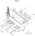
- Fig. 1 is a perspective view illustrating the appearance of the current sensor according to the embodiment.
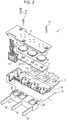
- Fig. 2 is a perspective view illustrating a state of the current sensor in which a lid, lid magnetic shields, and a board are disassembled.
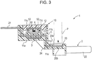
- Fig. 3 is a sectional view illustrating an inner structure of the current sensor taken along line III-III in Fig. 1 .
- Fig. 4 is a sectional view illustrating a sectional shape of a conductive portion taken along line IV-IV in Fig. 1 .
- the current sensor 1 As illustrated in Fig. 1 , the current sensor 1 according to the present embodiment includes three bus bars 2 through which a current to be measured flows and a casing 10 integrated with parts of the three bus bars 2. Conductive portions 20 for a performance check are provided in the casing 10. The conductive portions 20 are used to verify whether the current sensor 1 normally functions.
- the bus bars 2 are each formed by, for example, punching a metal plate of copper, a copper alloy, or the like by pressing or the like, and then, bending the metal plate into a predetermined shape. As illustrated in Figs. 1 and 2 , a pair of terminals 21, 22 are formed at respective ends of the bus bar 2. Another device (not illustrated) is to be connected to the pair of terminals 21, 22. The pair of terminals 21, 22 are exposed from a surface of the casing 10.
- the terminal 21 being one of the pair of terminals 21, 22 is a crimp-type terminal to be removably connected to the other device and has a through hole 23 through which a bolt is to be inserted for fastening to the other device.
- the crimp-type terminals 21 are arranged in the transverse direction so as to be aligned with each other at front faces and rear faces (coplanar with each other).
- the terminal 22 being another of the pair of terminals 21, 22 is the welding-type terminal 22 to be connected to the other device by welding.
- the welding-type terminals 22 are bent such that front faces and rear faces face each other (parallel to each other).
- the welding-type terminal 22 are arranged in the transverse direction.
- the casing 10 includes a box-shaped casing main body 11 having an open upper face and a lid 12 that covers the upper face of the casing main body 11.
- Both the casing main body 11 and the lid 12 are formed of insulative synthetic resin.
- the synthetic resin for example, resin having a good heat resistance such as polyphenylene sulfide (PPS) is used.
- PPS polyphenylene sulfide
- an elastomer or the like may be mixed.
- the bus bars 2 and main body-side magnetic shields 3 are secured at respective predetermined positions in a bottom portion 11a of the casing main body 11 by integral molding.
- the positional relationships between the bus bars 2 and the main body-side magnetic shields 3 are held, and accordingly, accuracy of the current sensor 1 is stabilized.
- the bus bars 2 and the main body-side magnetic shields 3 are disposed in an injection mold (not illustrated, similarly not illustrated hereinafter) in a state in which three bus bars 2 are disposed parallel to each other and arranged in the transverse direction as described above and the main body-side magnetic shields 3 are disposed at the positions facing rear faces of the respective bus bars 2. Then, the bus bars 2 and the main body-side magnetic shields 3 are integrated with synthetic resin injected around the bus bars 2 and the main body-side magnetic shields 3 by molding.
- three magnetic sensors 50 and a single terminal unit 51 are mounted on a common circuit board 5 and housed in an interior 11b of the casing main body 11.
- the terminal unit 51 is connecting terminals through which signals of the magnetic sensors 50 are output to the outside.
- the circuit board 5 is positioned relative to and secured to the casing main body 11 when positioning pins 11c projecting from the bottom portion 11a of the casing main body 11 are inserted through positioning holes 52 of the circuit board 5.
- the magnetic sensors 50 detect an induction fields generated by currents flowing through the bus bars 2.
- the magnetic sensors 50 are disposed at respective positions facing front faces of the respective bus bars 2.
- magnetoresistance effect elements or Hall elements can be used as the magnetic sensors 50.
- the lid 12 is placed on the upper face of the casing main body 11 and secured to the casing main body 11 by securing screws 13.
- Lid magnetic shields 4 are also secured to the lid 12 by integral molding.
- the lid magnetic shields 4 are disposed at respective positions facing the front faces of the respective bus bars 2. In Fig. 2 , the lid magnetic shields 4 are separated from the lid 12.
- the conductive portions 20 are each provided at a position between a corresponding one of the welding-type terminals 22 and a position where an induction field is detected by a corresponding one of the magnetic sensors 50.
- the conductive portion 20 for a performance check is independently provided other than the terminals 21, 22 to be connected to the other device as described above, unlike the related art, it is not required that a current probe P be directly pushed against the welding-type terminal 22. Accordingly, deformation of or damage to the terminal 22 due to pushing of the current probe P can be prevented.
- the front face of the bus bar 2 is exposed from the casing main body 11 to form an exposed face 20a.
- the exposed face 20a is a portion against which the current probe P for a performance check is pushed in the vertical direction.
- the rear face of the bus bar 2 opposite the exposed face 20a is coated with the synthetic resin to form a coated face 20b.
- the coated face 20b opposite the exposed face 20a When the coated face 20b opposite the exposed face 20a is coated with the synthetic resin as described above, the coated face 20b can absorb a pushing force of the current probe P to be exerted on the exposed face 20a. Accordingly, since the current probe P can be strongly pushed, a correct performance check can be performed. In addition, deformation of or damage to the bus bar 2 due to the pushing force of the current probe P can be prevented.
- the exposed face 20a projects from a surface of the casing main body 11 at a boundary between the conductive portion 20 and the surface of the casing main body 11.
- the current probe P can be reliably brought into contact with the exposed face 20a of the conductive portion 20.
- a projecting amount t of the exposed face 20a is set to 0.01 to 0.05 mm.
- a resin wall portion 14 projecting from the surface of the casing main body 11 is formed between the conductive portions 20 adjacent to each other. Accordingly, the lengths of a creepage distance L and a spatial distance between the conductive portions 20 adjacent to each other along the resin wall portion 14 can be sufficiently obtained even when the linear distance between the adjacent conductive portions 20 is small. Thus, size reduction of the current sensor 1 with improved voltage resistance can be realized.
- a projecting amount h of the resin wall portion 14 is 1.8 mm, and the creepage distance L between the conductive portions 20 is 8.4 mm.
- the current probe P may be misaligned and brought into contact with a conductive portion 20 adjacent to the target conductive portions 20.
- the resin wall portion 14 even when the current probe P is misaligned, the current probe P is brought into contact with the resin wall portion 14 and stopped. Thus, mistaken contact of the current probe P with the adjacent conductive portion 20 can be prevented.
- resin wall portions 14 have a rectangular shape so as to surround the exposed faces 20a of the conductive portions 20.
- a range in which the current probe P can be brought into contact with the conductive portions 20 can be limited. Accordingly, the current probe P can be correctly positioned in a current flowing direction in the conductive portions 20, thereby accuracy of a performance check is improved.
- the conductive portion 20 has a trapezoidal shape in which the longer base is the exposed face 20a and the shorter base is the coated face 20b.
- a taper angle ⁇ of the edge faces 20c is set to 2 to 5°.
- the conductive portion 20 When a large current flows through the bus bar 2, the conductive portion 20 generates heat due to Joule heat and thermally expand. However, with the above-described structure, even when the conductive portion 20 thermally expands, the conductive portion 20 expands toward the exposed face side due to its sectional shape (trapezoidal shape). Thus, deformation of portions of the casing main body 11 around the conductive portion 20 can be reduced.
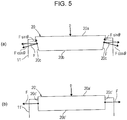
- Fig. 5 (a) is an explanatory view when the sectional shape of the conductive portion 20 is trapezoidal (present embodiment).
- Fig. 5 (b) is an explanatory view when the sectional shape of the conductive portion 20 is rectangular (comparative example).
- heat generation by the conductive portion 20' may soften the synthetic resin around the conductive portion 20'. Accordingly, the conductive portion 20' may sink into the casing main body 11' due to a pushing force p of the current probe P exerted on an exposed face 20a'.
- expansion forces F are applied to the edge faces 20c.
- these expansion forces F are each divided by a corresponding one of the reverse tapered edge faces 20c into an expansion force F ⁇ sin ⁇ in the edge face direction and an expansion force F ⁇ cos ⁇ in a direction perpendicular to the edge face direction.
- the expansion force F ⁇ sin ⁇ escapes in the edge face direction as described above.
- the expansion force F directly applied to the casing main body 11 is reduced to the expansion force F ⁇ cos ⁇ , and accordingly, deformation of the portions of the casing main body 11 around the conductive portion 20 can be reduced.
- the expansion force F ⁇ sin ⁇ in the edge face direction becomes a repulsive force against the pushing force p of the current probe P, sinking of the conductive portion 20 into the casing main body 11 can be prevented.
- Fig. 6 is a sectional view taken along line VI-VI in Fig. 1 , illustrating positions in contact with positioning jigs used for positioning the bus bars 2 are in contact.
- the casing main body 11 has removal holes 11d and pin holes 11e.
- the removal holes 11d are formed by positioning tools A used for positioning the bus bars 2 in the longitudinal direction and the transverse direction in the mold (not illustrated) when the bus bars 2 and the casing main body 11 are integrated by molding.
- the pin holes 11e are formed by using pressing pins B used for positioning the bus bars 2 in the longitudinal direction in the mold (not illustrated) when the bus bars 2 and the casing main body 11 are integrated by molding.
- the positioning tools A press side faces 2f and portions of the front faces 2d of the bus bars 2 loaded in the mold, thereby preventing misalignment of the bus bars 2 in the longitudinal direction and the transverse direction.
- the pressing pins B press portions of the rear faces 2e of the bus bars 2 loaded in the mold, thereby preventing misalignment of the bus bars 2 in the longitudinal direction.
- the removal holes 11d formed by the positioning tools A are preferably provided between bent portions 24 of the bus bars 2 and the conductive portions 20.
- the positions of the conductive portions 20 that influence accuracy of a performance check in the transverse direction can be disposed at correct positions relative to the casing main body 11.
- bus bars 2 are disposed parallel to each other, arranged in the transverse direction and integrated with the casing main body 11 by molding according to the above-described present embodiment, a structure in which a single bus bar 2 is integrated with the casing main body 11 by molding may be used.
- the number of the bus bars 2 is not limited to three. Any number of the bus bars 2 may be used.
- the exposed faces 20a of the conductive portions 20 are exposed from an upper face of the casing main body 11 in the longitudinal direction, this is not limiting.
- the exposed faces 20a may be exposed from a lower face in the longitudinal direction or side faces in the transverse direction of the casing main body 11.
- two bus bars 2 may be arranged such that thickness side faces of the bus bars 2 disposed in the longitudinal direction so as to be parallel to each other.
- the exposed faces 20a are respectively exposed from the left and right side faces of the casing main body 11 in the transverse direction.
- the rear face of the bus bar 2 is entirely coated with the synthetic resin so as to form the coated face 20b, this is not limiting. It is sufficient that a region in the coated face 20b in which the pushing force p of the current probe P can be absorbed be coated. For example, a central portion of the rear face of the bus bar 2 may be exposed. In this case, a region other than this central portion is coated so as to form the coated face 20b.
- terminal 21 being one of the pair of terminals 21, 22 is the crimp-type terminal 21 and the terminal 22 being the other of the pair of terminals 21, 22 is the welding-type terminal 22, this is not limiting. All the terminals may be welding-type terminal or crimp-type terminals.
- the resin wall portion 14 has a rectangular shape so as to surround the exposed face 20a of the conductive portion 20, this is not limiting.
- the resin wall portion 14 may have a different shape such as a circular shape as long as the current probe P can be correctly positioned in the conductive portion 20.
Landscapes
- Physics & Mathematics (AREA)
- General Physics & Mathematics (AREA)
- Engineering & Computer Science (AREA)
- Power Engineering (AREA)
- Measuring Instrument Details And Bridges, And Automatic Balancing Devices (AREA)
Abstract
Description
- The present invention relates to a current sensor that calculates a current value in accordance with a magnetic field generated by a current to be measured.
- As a current sensor that calculates a current value in accordance with a magnetic field generated by a current to be measured, a current sensor described in
PTL 1 is known. The current sensor described inPTL 1 includes a bus bar through which a current to be measured flows, a magnetic sensor that measures an induction field generated by the current to be measured, and a casing that houses the magnetic sensor and that is integrated with the bus bar. Both ends of the bus bar are exposed from a surface of the casing as terminals to be connected to another device such as a three-phase current motor. - A current sensor of this type is subjected to a performance check for checking whether the current sensor normally functions as specified in a product specification at a last stage of a manufacturing process. This performance check is performed through the terminals to be connected to the other device.
- Specifically, a current probe for a performance check is pushed against part of a terminal and a test current (300 to 1000 A) is flowed through the bus bar, and then, a current value flowing through the bus bar is actually measured and whether a value similar to the test current is indicated is checked. Here, a current sensor that indicates a different value from the test current and fails to pass the check undergoes adjustment of circuitry and a software constant, and the performance check is performed again on this current sensor.
- However, since the test current flowing through the bus bar is a large current, the current probe for a performance check is required to be pushed against part of the terminal of the bus bar with a strong force. Thus, it is unavoidable that a fine scratch is made on a surface of the terminal by a pushing force of the current probe.
- [PTL 1] Japanese Unexamined Patent Application Publication No.
2017-102022 - Meanwhile, in the current sensor of this type, terminals to which the other device is to be connected are roughly classified into the following two types. One of the two types is a type removably connected to a terminal of the other device similar to that of the current sensor described in
PTL 1, that is, a crimp-type terminal fastened by a bolt or the like. Another type is a type not removable from the terminal of the other device, that is, a welding-type terminal connected by welding. - With the welding-type terminal, misalignment due to deformation of the terminal or damage to the surface causes poor welding. Thus, a current sensor with the welding-type terminal is required to be handled more carefully than with that of the type having a crimp-type terminal such as the current sensor described in
PTL 1. - In a situation as described above, in a method by which the current probe is pushed against part of the terminal similarly to the method of related art, there is inconvenience in which deformation of or damage to the welding-type terminal may be caused even by a temporary connection.
- Accordingly, an object of the present invention is to provide a current sensor in which deformation of or damage to a terminal to be connected to another device can be prevented in a performance check for the current sensor and which can ensure ease of the performance check. Solution to Problem
- In order to achieve the above-described object, a current sensor according to the present invention includes at least one bus bar, a magnetic sensor, and a casing. The at least one bus bar has a pair of terminals to be connected to another device. The magnetic sensor is configured to detect an induction field generated by a current flowing through the at least one bus bar. The casing houses the magnetic sensor, is integrated with the at least one bus bar with the pair of terminals exposed, and is formed of synthetic resin. The at least one bus bar has a conductive portion for a performance check that includes an exposed face and a coated face. The exposed face is disposed such that at least part of a front face of the exposed face is exposed from the casing. The coated face is formed by coating with the casing at least part of a rear face opposite the exposed face. A length of the exposed face is greater than a length of the coated face in a sectional shape perpendicular to a current flowing direction, and edge faces that connect the exposed face and the coated face to each other such that each of the edge faces connects a corresponding one of ends of the exposed face and a corresponding one of ends of the coated face to each other form a reverse tapered shape in which a distance between the edge faces increases from the coated face toward the exposed face. The exposed face projects from a surface of the casing at a boundary between the conductive portion and the surface of the casing.
- In the current sensor according to the present invention, the conductive portion for a performance check includes the exposed face and the coated face, and the current probe for a performance check can be pushed against this exposed face. In this case, even when the current probe is strongly pushed against the exposed face, this force can be received by the coated face. Accordingly, since the current probe can be strongly pushed, a correct performance check can be performed. In addition, deformation of or damage to the terminals can be prevented.
- Furthermore, the exposed face projects from the surface of the casing at the boundary between the conductive portion and the surface of the casing. Thus, the current probe can be reliably brought into contact with the exposed face of the conductive portion.
- Furthermore, in a sectional shape perpendicular to the current flowing direction, the conductive portion for a performance check has a trapezoidal shape in which the length of the exposed face is greater than the length of the coated face. When a large current flows through the bus bar, the conductive portion generates heat due to Joule heat and thermally expands. However, the conductive portion expands toward the exposed face side due to the sectional shape of the exposed face. Thus, deformation of portions of the casing around the exposed face can be reduced.
- Furthermore, in the current sensor according to the present invention, the at least one of the pair of terminals is preferably a welding-type terminal to be connected to the other device by welding. In this case, the conductive portion is provided at a position between the welding-type terminal and a position where the induction field is to be detected by the magnetic sensor.
- With this structure, it is not required that the current probe be directly pushed against the welding-type terminal, and accordingly, deformation of or damage to the welding-type terminal due to pushing of the current probe can be prevented. Furthermore, when the conductive portion is provided between the welding-type terminal and a position where the induction field is to be detected, the performance check can be performed in a state close to a state in which the current sensor is attached to the other device.
- Furthermore, in the current sensor according to the present invention, the at least one bus bar preferably includes a plurality of bus bars disposed in the current flowing direction so as to be parallel to each other. In this case, the casing includes at least one resin wall portion that is disposed between the conductive portions of the plurality of bus bars adjacent to each other and that projects further than the exposed face. With this structure, the lengths of a creepage distance and a spatial distance between the conductive portions adjacent to each other along the at least one resin wall portion can be sufficiently obtained even when the linear distance between the adjacent conductive portions is small. Thus, size reduction of the current sensor with improved voltage resistance can be realized.
- Furthermore, in the case where the linear distance between the adjacent conductive portions is small, during an operation to push the current probe against a target conductive portion, when the operation is incorrectly performed, the current probe may be misaligned and brought into contact with a conductive portion adjacent to the target conductive portions. However, with this structure, even when the current probe is misaligned, the current probe is brought into contact with the at least one resin wall portion and stopped. Thus, mistaken contact of the current probe with the adjacent conductive portion can be prevented.
- Furthermore, in the current sensor according to the present invention, the at least one resin wall portion preferably includes a plurality of resin wall portions formed so as to surround the respective conductive portions. With this, a range in which the current probe can be brought into contact with each of the conductive portions can be limited. Accordingly, the current probe can be correctly positioned in the current flowing direction in the conductive portion, thereby accuracy of a performance check is improved.
- Furthermore, in the current sensor according to the present invention, the at least one bus bar preferably has a bent portion between the conductive portion and a position where the induction field is to be detected by the magnetic sensor. In this case, the casing has a positioning-tool removal hole that allows part of one of the edge faces of the at least one bus bar and part of a front face of the at least one bus bar to be exposed to outside at a position between the bent portion of the at least one bus bar and the conductive portion of the at least one bus bar.
- With this structure, a position in contact with the positioning tool used for positioning the at least one bus bar is provided coplanar with the conductive portion. Thus, when injection molding of resin is performed with the at least one bus bar and the casing integrated, the exposed face of the conductive portion that influences accuracy of a performance check can be disposed at correct positions relative to the casing.
- In the current sensor according to the present invention, the conductive portion for the performance check is provided in addition to the terminals to be connected to the other device. In this way, deformation of or damage to the terminal to be connected to the other device can be prevented and ease of the performance check can be ensured.
-
- [
Fig. 1] Fig. 1 is a perspective view illustrating the appearance of a current sensor that is an example of an embodiment according to the present invention. - [
Fig. 2] Fig. 2 is an explanatory view illustrating the current sensor illustrated inFig. 1 with a lid removed. - [
Fig. 3] Fig. 3 is a sectional view taken along line III-III inFig. 1 . - [
Fig. 4] Fig. 4 is a sectional view taken along line IV-IV inFig. 1 . - [
Fig. 5] Fig. 5 includes explanatory views illustrating states in which a conductive portion have thermally expanded. - [
Fig. 6] Fig. 6 is a sectional view taken along line VI-VI inFig. 1 . - Next, a current sensor that is an example of an embodiment of the present invention is described with reference to
Figs. 1 to 6 . Acurrent sensor 1 according to the present embodiment can be used for devices that require large current such as controllers used for, for example, hybrid vehicles and electric vehicles. In the description, a direction in which the current flows is defined as an extension direction (Y direction inFig. 1 ), a direction in which bus bars are arranged is defined as a transverse direction (X direction inFig. 1 ), and a direction perpendicular to the transverse direction when seen from the extension direction is defined as a longitudinal direction (Z direction inFig. 1 ). -
Fig. 1 is a perspective view illustrating the appearance of the current sensor according to the embodiment.Fig. 2 is a perspective view illustrating a state of the current sensor in which a lid, lid magnetic shields, and a board are disassembled.Fig. 3 is a sectional view illustrating an inner structure of the current sensor taken along line III-III inFig. 1 .Fig. 4 is a sectional view illustrating a sectional shape of a conductive portion taken along line IV-IV inFig. 1 . - As illustrated in
Fig. 1 , thecurrent sensor 1 according to the present embodiment includes threebus bars 2 through which a current to be measured flows and acasing 10 integrated with parts of the threebus bars 2.Conductive portions 20 for a performance check are provided in thecasing 10. Theconductive portions 20 are used to verify whether thecurrent sensor 1 normally functions. - The bus bars 2 are each formed by, for example, punching a metal plate of copper, a copper alloy, or the like by pressing or the like, and then, bending the metal plate into a predetermined shape. As illustrated in
Figs. 1 and2 , a pair ofterminals bus bar 2. Another device (not illustrated) is to be connected to the pair ofterminals terminals casing 10. - The terminal 21 being one of the pair of
terminals hole 23 through which a bolt is to be inserted for fastening to the other device. The crimp-type terminals 21 are arranged in the transverse direction so as to be aligned with each other at front faces and rear faces (coplanar with each other). - The terminal 22 being another of the pair of
terminals type terminal 22 to be connected to the other device by welding. The welding-type terminals 22 are bent such that front faces and rear faces face each other (parallel to each other). The welding-type terminal 22 are arranged in the transverse direction. - As illustrated in
Fig. 2 , thecasing 10 includes a box-shaped casingmain body 11 having an open upper face and alid 12 that covers the upper face of the casingmain body 11. Both the casingmain body 11 and thelid 12 are formed of insulative synthetic resin. As the synthetic resin, for example, resin having a good heat resistance such as polyphenylene sulfide (PPS) is used. Furthermore, for improvement of toughness, an elastomer or the like may be mixed. - As illustrated in
Fig. 3 , thebus bars 2 and main body-sidemagnetic shields 3 are secured at respective predetermined positions in abottom portion 11a of the casingmain body 11 by integral molding. Thus, the positional relationships between thebus bars 2 and the main body-sidemagnetic shields 3 are held, and accordingly, accuracy of thecurrent sensor 1 is stabilized. - According to the present embodiment, the
bus bars 2 and the main body-sidemagnetic shields 3 are disposed in an injection mold (not illustrated, similarly not illustrated hereinafter) in a state in which threebus bars 2 are disposed parallel to each other and arranged in the transverse direction as described above and the main body-sidemagnetic shields 3 are disposed at the positions facing rear faces of the respective bus bars 2. Then, thebus bars 2 and the main body-sidemagnetic shields 3 are integrated with synthetic resin injected around thebus bars 2 and the main body-sidemagnetic shields 3 by molding. - As illustrated in
Figs. 2 and3 , threemagnetic sensors 50 and a singleterminal unit 51 are mounted on acommon circuit board 5 and housed in an interior 11b of the casingmain body 11. Theterminal unit 51 is connecting terminals through which signals of themagnetic sensors 50 are output to the outside. Furthermore, thecircuit board 5 is positioned relative to and secured to the casingmain body 11 when positioning pins 11c projecting from thebottom portion 11a of the casingmain body 11 are inserted through positioning holes 52 of thecircuit board 5. - The
magnetic sensors 50 detect an induction fields generated by currents flowing through the bus bars 2. Themagnetic sensors 50 are disposed at respective positions facing front faces of the respective bus bars 2. Furthermore, as themagnetic sensors 50, for example, magnetoresistance effect elements or Hall elements can be used. - The
lid 12 is placed on the upper face of the casingmain body 11 and secured to the casingmain body 11 by securingscrews 13. Lidmagnetic shields 4 are also secured to thelid 12 by integral molding. The lidmagnetic shields 4 are disposed at respective positions facing the front faces of the respective bus bars 2. InFig. 2 , the lidmagnetic shields 4 are separated from thelid 12. - As illustrated in
Figs. 1 and2 , theconductive portions 20 are each provided at a position between a corresponding one of the welding-type terminals 22 and a position where an induction field is detected by a corresponding one of themagnetic sensors 50. When theconductive portion 20 for a performance check is independently provided other than theterminals type terminal 22. Accordingly, deformation of or damage to the terminal 22 due to pushing of the current probe P can be prevented. - Furthermore, as illustrated in
Fig. 3 , in theconductive portion 20, the front face of thebus bar 2 is exposed from the casingmain body 11 to form an exposedface 20a. The exposedface 20a is a portion against which the current probe P for a performance check is pushed in the vertical direction. Furthermore, in theconductive portion 20, the rear face of thebus bar 2 opposite the exposedface 20a is coated with the synthetic resin to form acoated face 20b. - When the
coated face 20b opposite the exposedface 20a is coated with the synthetic resin as described above, thecoated face 20b can absorb a pushing force of the current probe P to be exerted on the exposedface 20a. Accordingly, since the current probe P can be strongly pushed, a correct performance check can be performed. In addition, deformation of or damage to thebus bar 2 due to the pushing force of the current probe P can be prevented. - As illustrated in
Fig. 4 , the exposedface 20a projects from a surface of the casingmain body 11 at a boundary between theconductive portion 20 and the surface of the casingmain body 11. Thus, the current probe P can be reliably brought into contact with the exposedface 20a of theconductive portion 20. According to the present embodiment, a projecting amount t of the exposedface 20a is set to 0.01 to 0.05 mm. - Furthermore, according to the present embodiment, a
resin wall portion 14 projecting from the surface of the casingmain body 11 is formed between theconductive portions 20 adjacent to each other. Accordingly, the lengths of a creepage distance L and a spatial distance between theconductive portions 20 adjacent to each other along theresin wall portion 14 can be sufficiently obtained even when the linear distance between the adjacentconductive portions 20 is small. Thus, size reduction of thecurrent sensor 1 with improved voltage resistance can be realized. - According to the present embodiment, a projecting amount h of the
resin wall portion 14 is 1.8 mm, and the creepage distance L between theconductive portions 20 is 8.4 mm. However, this is not limiting. It is sufficient that the projecting amount h and the creepage distance L be such distances that electrical insulation against a value of a current flowing through thebus bar 2 can be obtained. - Furthermore, in the case where the linear distance between the adjacent
conductive portions 20 is small, during an operation to push the current probe P against a targetconductive portion 20, when the operation is incorrectly performed, the current probe P may be misaligned and brought into contact with aconductive portion 20 adjacent to the targetconductive portions 20. However, with theresin wall portion 14, even when the current probe P is misaligned, the current probe P is brought into contact with theresin wall portion 14 and stopped. Thus, mistaken contact of the current probe P with the adjacentconductive portion 20 can be prevented. - As illustrated in
Figs. 1 and2 , according to the present embodiment,resin wall portions 14 have a rectangular shape so as to surround the exposed faces 20a of theconductive portions 20. Thus, a range in which the current probe P can be brought into contact with theconductive portions 20 can be limited. Accordingly, the current probe P can be correctly positioned in a current flowing direction in theconductive portions 20, thereby accuracy of a performance check is improved. - Furthermore, as illustrated in
Fig. 4 , in the sectional shape taken along line IV-IV inFig. 1 , theconductive portion 20 has a trapezoidal shape in which the longer base is the exposedface 20a and the shorter base is thecoated face 20b. The distance between a pair of edge faces 20c serving as the legs of this trapezoid both increases to form a reverse tapered shape from thecoated face 20b toward the exposedface 20a, and the edge faces 20c are connected. According to the present embodiment, a taper angle θ of the edge faces 20c is set to 2 to 5°. - When a large current flows through the
bus bar 2, theconductive portion 20 generates heat due to Joule heat and thermally expand. However, with the above-described structure, even when theconductive portion 20 thermally expands, theconductive portion 20 expands toward the exposed face side due to its sectional shape (trapezoidal shape). Thus, deformation of portions of the casingmain body 11 around theconductive portion 20 can be reduced. - Next, a state in which the
conductive portion 20 has thermally expanded is described with reference toFig. 5. Fig. 5 (a) is an explanatory view when the sectional shape of theconductive portion 20 is trapezoidal (present embodiment).Fig. 5 (b) is an explanatory view when the sectional shape of theconductive portion 20 is rectangular (comparative example). - As illustrated in
Fig. 5 (b) , in the case where the sectional shape of a conductive portion 20' is rectangular, when a large current flows through a bus bar 2' and the conductive portion 20' thermally expands, expansion forces F are applied to edge faces 20c'. This may lead to deformation or cracking in portions of a casing main body 11' around the edge faces 20c'. - Furthermore, heat generation by the conductive portion 20' may soften the synthetic resin around the conductive portion 20'. Accordingly, the conductive portion 20' may sink into the casing main body 11' due to a pushing force p of the current probe P exerted on an exposed
face 20a'. - Meanwhile, as illustrated in
Fig. 5 (a) , in the case where the sectional shape of theconductive portion 20 is trapezoidal, when a large current flows through thebus bar 2, and theconductive portion 20 thermally expands, expansion forces F are applied to the edge faces 20c. However, these expansion forces F are each divided by a corresponding one of the reverse tapered edge faces 20c into an expansion force F·sin θ in the edge face direction and an expansion force F·cos θ in a direction perpendicular to the edge face direction. - Of the expansion force F applied to the reverse tapered
edge face 20c, the expansion force F·sin θ escapes in the edge face direction as described above. Thus, the expansion force F directly applied to the casingmain body 11 is reduced to the expansion force F·cos θ, and accordingly, deformation of the portions of the casingmain body 11 around theconductive portion 20 can be reduced. Furthermore, since the expansion force F·sin θ in the edge face direction becomes a repulsive force against the pushing force p of the current probe P, sinking of theconductive portion 20 into the casingmain body 11 can be prevented. -
Fig. 6 is a sectional view taken along line VI-VI inFig. 1 , illustrating positions in contact with positioning jigs used for positioning the bus bars 2 are in contact. The casingmain body 11 hasremoval holes 11d andpin holes 11e. The removal holes 11d are formed by positioning tools A used for positioning thebus bars 2 in the longitudinal direction and the transverse direction in the mold (not illustrated) when thebus bars 2 and the casingmain body 11 are integrated by molding. The pin holes 11e are formed by using pressing pins B used for positioning thebus bars 2 in the longitudinal direction in the mold (not illustrated) when thebus bars 2 and the casingmain body 11 are integrated by molding. - According to the present embodiment, as illustrated in
Fig. 6 , the positioning tools A press side faces 2f and portions of the front faces 2d of thebus bars 2 loaded in the mold, thereby preventing misalignment of thebus bars 2 in the longitudinal direction and the transverse direction. The pressing pins B press portions of the rear faces 2e of thebus bars 2 loaded in the mold, thereby preventing misalignment of thebus bars 2 in the longitudinal direction. - Also according to the present embodiment, as illustrated in
Fig. 3 , theremoval holes 11d formed by the positioning tools A are preferably provided betweenbent portions 24 of thebus bars 2 and theconductive portions 20. Thus, the positions of theconductive portions 20 that influence accuracy of a performance check in the transverse direction can be disposed at correct positions relative to the casingmain body 11. - Although three
bus bars 2 are disposed parallel to each other, arranged in the transverse direction and integrated with the casingmain body 11 by molding according to the above-described present embodiment, a structure in which asingle bus bar 2 is integrated with the casingmain body 11 by molding may be used. The number of the bus bars 2 is not limited to three. Any number of the bus bars 2 may be used. - Although the exposed faces 20a of the
conductive portions 20 are exposed from an upper face of the casingmain body 11 in the longitudinal direction, this is not limiting. The exposed faces 20a may be exposed from a lower face in the longitudinal direction or side faces in the transverse direction of the casingmain body 11. For example, twobus bars 2 may be arranged such that thickness side faces of thebus bars 2 disposed in the longitudinal direction so as to be parallel to each other. In this case, the exposed faces 20a are respectively exposed from the left and right side faces of the casingmain body 11 in the transverse direction. - Although the rear face of the
bus bar 2 is entirely coated with the synthetic resin so as to form thecoated face 20b, this is not limiting. It is sufficient that a region in thecoated face 20b in which the pushing force p of the current probe P can be absorbed be coated. For example, a central portion of the rear face of thebus bar 2 may be exposed. In this case, a region other than this central portion is coated so as to form thecoated face 20b. - Furthermore, although the terminal 21 being one of the pair of
terminals type terminal 21 and the terminal 22 being the other of the pair ofterminals type terminal 22, this is not limiting. All the terminals may be welding-type terminal or crimp-type terminals. - Furthermore, although the
resin wall portion 14 has a rectangular shape so as to surround the exposedface 20a of theconductive portion 20, this is not limiting. Theresin wall portion 14 may have a different shape such as a circular shape as long as the current probe P can be correctly positioned in theconductive portion 20. -
- 1
- current sensor
- 2
- bus bar
- 3
- main body-side magnetic shield
- 4
- lid magnetic shield
- 5
- circuit board
- 10
- casing
- 11
- casing main body
- 11d
- removal hole (positioning-tool removal hole)
- 12
- lid
- 14
- resin wall portion
- 20
- conductive portion
- 20a
- exposed face
- 20b
- coated face
- 20c
- edge face
- 21
- crimp-type terminal
- 22
- welding-type terminal
- 50
- magnetic sensor
- P
- current probe
- A
- positioning tool
- B
- pressing pin
Claims (5)
- A current sensor comprising:at least one bus bar that has a pair of terminals to be connected to another device;a magnetic sensor configured to detect an induction field generated by a current flowing through the at least one bus bar; anda casing that houses the magnetic sensor, that is integrated with the at least one bus bar with the pair of terminals exposed, and that is formed of synthetic resin, whereinthe at least one bus bar has a conductive portion for a performance check that includes an exposed face disposed such that at least part of a front face of the exposed face is exposed from the casing and a coated face formed by coating with the casing at least part of a rear face opposite the exposed face, whereina length of the exposed face is greater than a length of the coated face in a sectional shape perpendicular to a current flowing direction, and edge faces that connect the exposed face and the coated face to each other such that each of the edge faces connects a corresponding one of ends of the exposed face and a corresponding one of ends of the coated face to each other form a reverse tapered shape in which a distance between the edge faces increases from the coated face toward the exposed face, and whereinthe exposed face projects from a surface of the casing at a boundary between the conductive portion and the surface of the casing.
- The current sensor according to Claim 1, wherein
at least one of the pair of terminals is a welding-type terminal to be connected to the other device by welding, and wherein
the conductive portion is provided at a position between the welding-type terminal and a position where the induction field is to be detected by the magnetic sensor. - The current sensor according to Claim 1 or 2, wherein
the at least one bus bar includes a plurality of bus bars disposed in the current flowing direction so as to be parallel to each other, and wherein
the casing includes at least one resin wall portion that is disposed between the conductive portions of the plurality of bus bars adjacent to each other and that projects further than the exposed face. - The current sensor according to Claim 3, wherein
the at least one resin wall portion includes a plurality of resin wall portions formed so as to surround the respective conductive portions. - The current sensor according to any one of Claims 1 to 4, wherein
the at least one bus bar has a bent portion between the conductive portion and a position where the induction field is to be detected by the magnetic sensor, and wherein
the casing has a positioning-tool removal hole that allows part of one of the edge faces of the at least one bus bar and part of a front face of the at least one bus bar to be exposed to outside at a position between the bent portion of the at least one bus bar and the conductive portion of the at least one bus bar.
Applications Claiming Priority (2)
| Application Number | Priority Date | Filing Date | Title |
|---|---|---|---|
| JP2017238462 | 2017-12-13 | ||
| PCT/JP2018/045571 WO2019117170A1 (en) | 2017-12-13 | 2018-12-11 | Current sensor |
Publications (3)
| Publication Number | Publication Date |
|---|---|
| EP3726229A1 true EP3726229A1 (en) | 2020-10-21 |
| EP3726229A4 EP3726229A4 (en) | 2021-09-08 |
| EP3726229B1 EP3726229B1 (en) | 2022-06-22 |
Family
ID=66819349
Family Applications (1)
| Application Number | Title | Priority Date | Filing Date |
|---|---|---|---|
| EP18889183.2A Active EP3726229B1 (en) | 2017-12-13 | 2018-12-11 | Current sensor |
Country Status (5)
| Country | Link |
|---|---|
| US (1) | US11150274B2 (en) |
| EP (1) | EP3726229B1 (en) |
| JP (1) | JP6841939B2 (en) |
| CN (1) | CN212646790U (en) |
| WO (1) | WO2019117170A1 (en) |
Families Citing this family (3)
| Publication number | Priority date | Publication date | Assignee | Title |
|---|---|---|---|---|
| US11754426B2 (en) * | 2019-01-04 | 2023-09-12 | Westinghouse Air Brake Technologies Corporation | Transducer sensor system |
| CN114556115B (en) | 2019-10-08 | 2025-04-08 | 阿尔卑斯阿尔派株式会社 | Magnetic sensor and current detection device provided with same |
| CN113030546B (en) * | 2019-12-25 | 2025-04-25 | 阿尔卑斯阿尔派株式会社 | Current Sensors |
Family Cites Families (19)
| Publication number | Priority date | Publication date | Assignee | Title |
|---|---|---|---|---|
| JPH05126865A (en) * | 1991-10-22 | 1993-05-21 | Hitachi Ltd | Device or method for detecting current |
| DE10392295T5 (en) * | 2002-04-04 | 2005-05-19 | Hitachi, Ltd. | Power converter and thus equipped electric drive and thus equipped mobile device |
| JP4812311B2 (en) * | 2005-03-10 | 2011-11-09 | Jx日鉱日石エネルギー株式会社 | Dye-sensitized solar cell |
| JP2007265962A (en) * | 2006-02-28 | 2007-10-11 | Hitachi Ltd | Laser welding method, control unit manufacturing method, and vehicle control unit |
| JP2007329035A (en) * | 2006-06-08 | 2007-12-20 | Mitsuba Corp | Connecting terminal |
| JP4861155B2 (en) * | 2006-12-20 | 2012-01-25 | 矢崎総業株式会社 | Current sensor and molding method thereof |
| JP4912172B2 (en) * | 2007-02-01 | 2012-04-11 | Jx日鉱日石エネルギー株式会社 | Composite nanorod substrate and photoelectric conversion device using the same |
| JP2010101751A (en) * | 2008-10-23 | 2010-05-06 | Toyota Motor Corp | Probing inspection device and probing inspection method |
| JP5482736B2 (en) * | 2011-06-28 | 2014-05-07 | 株式会社デンソー | Current sensor |
| WO2013136751A1 (en) * | 2012-03-16 | 2013-09-19 | キヤノン電子株式会社 | Measurement module, electronic apparatus, power source tap, power source unit, and embedded measurement module |
| JP6030866B2 (en) * | 2012-06-14 | 2016-11-24 | 矢崎総業株式会社 | Current sensor |
| JP2014078408A (en) * | 2012-10-11 | 2014-05-01 | Tokai Rika Co Ltd | Bus bar structure, and current sensor using the same |
| JP6477089B2 (en) | 2014-05-23 | 2019-03-06 | 株式会社デンソー | Bus bar module with current sensor |
| JP6462850B2 (en) * | 2015-03-17 | 2019-01-30 | アルプス電気株式会社 | Current sensor |
| WO2017014040A1 (en) * | 2015-07-22 | 2017-01-26 | 株式会社村田製作所 | Current sensor |
| JP6402089B2 (en) | 2015-12-02 | 2018-10-10 | アルプス電気株式会社 | Current sensor |
| JP6302453B2 (en) | 2015-12-02 | 2018-03-28 | アルプス電気株式会社 | Current sensor |
| JP6711086B2 (en) * | 2016-04-01 | 2020-06-17 | 日立金属株式会社 | Current sensor |
| JP6651956B2 (en) * | 2016-04-01 | 2020-02-19 | 日立金属株式会社 | Current sensor |
-
2018
- 2018-12-11 JP JP2019559674A patent/JP6841939B2/en active Active
- 2018-12-11 CN CN201890001410.XU patent/CN212646790U/en active Active
- 2018-12-11 WO PCT/JP2018/045571 patent/WO2019117170A1/en not_active Ceased
- 2018-12-11 EP EP18889183.2A patent/EP3726229B1/en active Active
-
2020
- 2020-06-12 US US16/899,879 patent/US11150274B2/en active Active
Also Published As
| Publication number | Publication date |
|---|---|
| CN212646790U (en) | 2021-03-02 |
| WO2019117170A1 (en) | 2019-06-20 |
| US11150274B2 (en) | 2021-10-19 |
| EP3726229A4 (en) | 2021-09-08 |
| JP6841939B2 (en) | 2021-03-10 |
| JPWO2019117170A1 (en) | 2020-10-01 |
| EP3726229B1 (en) | 2022-06-22 |
| US20200309822A1 (en) | 2020-10-01 |
Similar Documents
| Publication | Publication Date | Title |
|---|---|---|
| CN111886507B (en) | Integrated current measuring device | |
| US11150274B2 (en) | Current sensor | |
| EP2746782B1 (en) | Current sensor and manufacturing method for the same | |
| US9086440B2 (en) | Current sensor | |
| EP3367109B1 (en) | Shunt resistor | |
| EP3726228B1 (en) | Current sensor | |
| US8371884B2 (en) | Device and method for connecting at least two electric terminals | |
| US11366139B2 (en) | Device and method for mounting a magnetic field sensor chip on a busbar | |
| KR102955264B1 (en) | Electrical device for receiving a magnetic field measurement sensor | |
| CN103635816A (en) | Current detection device | |
| WO2012157362A1 (en) | Current detecting apparatus | |
| US20150287511A1 (en) | Connector device | |
| JP2015005473A (en) | Bus bar and manufacturing method of the same | |
| US9410991B2 (en) | Attachment structure of current sensor and electric conductive member | |
| JP2018191452A (en) | Electrical connection box | |
| KR102095767B1 (en) | Measurement of current in the insulated body | |
| US20190393629A1 (en) | Control unit having press-fit structure | |
| US12112870B2 (en) | Shunt resistor | |
| US10670636B2 (en) | Current detection device | |
| US20090273906A1 (en) | Transport housing for an electronic flat module | |
| KR101049052B1 (en) | Multi type current sensor | |
| US10218104B2 (en) | Connector with a spring terminal ensuring reliable connection to a mating terminal | |
| JP2010203910A (en) | Current sensor and method of manufacturing the same | |
| US20240372308A1 (en) | Method for producing a contact unit, and contact unit | |
| CN113039685A (en) | Circuit structure |
Legal Events
| Date | Code | Title | Description |
|---|---|---|---|
| STAA | Information on the status of an ep patent application or granted ep patent |
Free format text: STATUS: THE INTERNATIONAL PUBLICATION HAS BEEN MADE |
|
| PUAI | Public reference made under article 153(3) epc to a published international application that has entered the european phase |
Free format text: ORIGINAL CODE: 0009012 |
|
| STAA | Information on the status of an ep patent application or granted ep patent |
Free format text: STATUS: REQUEST FOR EXAMINATION WAS MADE |
|
| 17P | Request for examination filed |
Effective date: 20200708 |
|
| AK | Designated contracting states |
Kind code of ref document: A1 Designated state(s): AL AT BE BG CH CY CZ DE DK EE ES FI FR GB GR HR HU IE IS IT LI LT LU LV MC MK MT NL NO PL PT RO RS SE SI SK SM TR |
|
| AX | Request for extension of the european patent |
Extension state: BA ME |
|
| DAV | Request for validation of the european patent (deleted) | ||
| DAX | Request for extension of the european patent (deleted) | ||
| A4 | Supplementary search report drawn up and despatched |
Effective date: 20210810 |
|
| RIC1 | Information provided on ipc code assigned before grant |
Ipc: G01R 15/20 20060101AFI20210804BHEP |
|
| GRAP | Despatch of communication of intention to grant a patent |
Free format text: ORIGINAL CODE: EPIDOSNIGR1 |
|
| STAA | Information on the status of an ep patent application or granted ep patent |
Free format text: STATUS: GRANT OF PATENT IS INTENDED |
|
| RIC1 | Information provided on ipc code assigned before grant |
Ipc: G01R 19/00 20060101ALI20220110BHEP Ipc: G01R 15/20 20060101AFI20220110BHEP |
|
| INTG | Intention to grant announced |
Effective date: 20220126 |
|
| GRAS | Grant fee paid |
Free format text: ORIGINAL CODE: EPIDOSNIGR3 |
|
| GRAA | (expected) grant |
Free format text: ORIGINAL CODE: 0009210 |
|
| STAA | Information on the status of an ep patent application or granted ep patent |
Free format text: STATUS: THE PATENT HAS BEEN GRANTED |
|
| AK | Designated contracting states |
Kind code of ref document: B1 Designated state(s): AL AT BE BG CH CY CZ DE DK EE ES FI FR GB GR HR HU IE IS IT LI LT LU LV MC MK MT NL NO PL PT RO RS SE SI SK SM TR |
|
| REG | Reference to a national code |
Ref country code: GB Ref legal event code: FG4D |
|
| REG | Reference to a national code |
Ref country code: CH Ref legal event code: EP |
|
| REG | Reference to a national code |
Ref country code: DE Ref legal event code: R096 Ref document number: 602018037168 Country of ref document: DE |
|
| REG | Reference to a national code |
Ref country code: AT Ref legal event code: REF Ref document number: 1500091 Country of ref document: AT Kind code of ref document: T Effective date: 20220715 |
|
| REG | Reference to a national code |
Ref country code: IE Ref legal event code: FG4D |
|
| REG | Reference to a national code |
Ref country code: LT Ref legal event code: MG9D |
|
| REG | Reference to a national code |
Ref country code: NL Ref legal event code: MP Effective date: 20220622 |
|
| PG25 | Lapsed in a contracting state [announced via postgrant information from national office to epo] |
Ref country code: SE Free format text: LAPSE BECAUSE OF FAILURE TO SUBMIT A TRANSLATION OF THE DESCRIPTION OR TO PAY THE FEE WITHIN THE PRESCRIBED TIME-LIMIT Effective date: 20220622 Ref country code: NO Free format text: LAPSE BECAUSE OF FAILURE TO SUBMIT A TRANSLATION OF THE DESCRIPTION OR TO PAY THE FEE WITHIN THE PRESCRIBED TIME-LIMIT Effective date: 20220922 Ref country code: LT Free format text: LAPSE BECAUSE OF FAILURE TO SUBMIT A TRANSLATION OF THE DESCRIPTION OR TO PAY THE FEE WITHIN THE PRESCRIBED TIME-LIMIT Effective date: 20220622 Ref country code: HR Free format text: LAPSE BECAUSE OF FAILURE TO SUBMIT A TRANSLATION OF THE DESCRIPTION OR TO PAY THE FEE WITHIN THE PRESCRIBED TIME-LIMIT Effective date: 20220622 Ref country code: GR Free format text: LAPSE BECAUSE OF FAILURE TO SUBMIT A TRANSLATION OF THE DESCRIPTION OR TO PAY THE FEE WITHIN THE PRESCRIBED TIME-LIMIT Effective date: 20220923 Ref country code: FI Free format text: LAPSE BECAUSE OF FAILURE TO SUBMIT A TRANSLATION OF THE DESCRIPTION OR TO PAY THE FEE WITHIN THE PRESCRIBED TIME-LIMIT Effective date: 20220622 Ref country code: BG Free format text: LAPSE BECAUSE OF FAILURE TO SUBMIT A TRANSLATION OF THE DESCRIPTION OR TO PAY THE FEE WITHIN THE PRESCRIBED TIME-LIMIT Effective date: 20220922 |
|
| REG | Reference to a national code |
Ref country code: AT Ref legal event code: MK05 Ref document number: 1500091 Country of ref document: AT Kind code of ref document: T Effective date: 20220622 |
|
| PG25 | Lapsed in a contracting state [announced via postgrant information from national office to epo] |
Ref country code: RS Free format text: LAPSE BECAUSE OF FAILURE TO SUBMIT A TRANSLATION OF THE DESCRIPTION OR TO PAY THE FEE WITHIN THE PRESCRIBED TIME-LIMIT Effective date: 20220622 Ref country code: LV Free format text: LAPSE BECAUSE OF FAILURE TO SUBMIT A TRANSLATION OF THE DESCRIPTION OR TO PAY THE FEE WITHIN THE PRESCRIBED TIME-LIMIT Effective date: 20220622 |
|
| PG25 | Lapsed in a contracting state [announced via postgrant information from national office to epo] |
Ref country code: NL Free format text: LAPSE BECAUSE OF FAILURE TO SUBMIT A TRANSLATION OF THE DESCRIPTION OR TO PAY THE FEE WITHIN THE PRESCRIBED TIME-LIMIT Effective date: 20220622 |
|
| PG25 | Lapsed in a contracting state [announced via postgrant information from national office to epo] |
Ref country code: SM Free format text: LAPSE BECAUSE OF FAILURE TO SUBMIT A TRANSLATION OF THE DESCRIPTION OR TO PAY THE FEE WITHIN THE PRESCRIBED TIME-LIMIT Effective date: 20220622 Ref country code: SK Free format text: LAPSE BECAUSE OF FAILURE TO SUBMIT A TRANSLATION OF THE DESCRIPTION OR TO PAY THE FEE WITHIN THE PRESCRIBED TIME-LIMIT Effective date: 20220622 Ref country code: RO Free format text: LAPSE BECAUSE OF FAILURE TO SUBMIT A TRANSLATION OF THE DESCRIPTION OR TO PAY THE FEE WITHIN THE PRESCRIBED TIME-LIMIT Effective date: 20220622 Ref country code: PT Free format text: LAPSE BECAUSE OF FAILURE TO SUBMIT A TRANSLATION OF THE DESCRIPTION OR TO PAY THE FEE WITHIN THE PRESCRIBED TIME-LIMIT Effective date: 20221024 Ref country code: ES Free format text: LAPSE BECAUSE OF FAILURE TO SUBMIT A TRANSLATION OF THE DESCRIPTION OR TO PAY THE FEE WITHIN THE PRESCRIBED TIME-LIMIT Effective date: 20220622 Ref country code: EE Free format text: LAPSE BECAUSE OF FAILURE TO SUBMIT A TRANSLATION OF THE DESCRIPTION OR TO PAY THE FEE WITHIN THE PRESCRIBED TIME-LIMIT Effective date: 20220622 Ref country code: CZ Free format text: LAPSE BECAUSE OF FAILURE TO SUBMIT A TRANSLATION OF THE DESCRIPTION OR TO PAY THE FEE WITHIN THE PRESCRIBED TIME-LIMIT Effective date: 20220622 Ref country code: AT Free format text: LAPSE BECAUSE OF FAILURE TO SUBMIT A TRANSLATION OF THE DESCRIPTION OR TO PAY THE FEE WITHIN THE PRESCRIBED TIME-LIMIT Effective date: 20220622 |
|
| PG25 | Lapsed in a contracting state [announced via postgrant information from national office to epo] |
Ref country code: PL Free format text: LAPSE BECAUSE OF FAILURE TO SUBMIT A TRANSLATION OF THE DESCRIPTION OR TO PAY THE FEE WITHIN THE PRESCRIBED TIME-LIMIT Effective date: 20220622 Ref country code: IS Free format text: LAPSE BECAUSE OF FAILURE TO SUBMIT A TRANSLATION OF THE DESCRIPTION OR TO PAY THE FEE WITHIN THE PRESCRIBED TIME-LIMIT Effective date: 20221022 |
|
| REG | Reference to a national code |
Ref country code: DE Ref legal event code: R097 Ref document number: 602018037168 Country of ref document: DE |
|
| PG25 | Lapsed in a contracting state [announced via postgrant information from national office to epo] |
Ref country code: AL Free format text: LAPSE BECAUSE OF FAILURE TO SUBMIT A TRANSLATION OF THE DESCRIPTION OR TO PAY THE FEE WITHIN THE PRESCRIBED TIME-LIMIT Effective date: 20220622 |
|
| PG25 | Lapsed in a contracting state [announced via postgrant information from national office to epo] |
Ref country code: DK Free format text: LAPSE BECAUSE OF FAILURE TO SUBMIT A TRANSLATION OF THE DESCRIPTION OR TO PAY THE FEE WITHIN THE PRESCRIBED TIME-LIMIT Effective date: 20220622 |
|
| PLBE | No opposition filed within time limit |
Free format text: ORIGINAL CODE: 0009261 |
|
| STAA | Information on the status of an ep patent application or granted ep patent |
Free format text: STATUS: NO OPPOSITION FILED WITHIN TIME LIMIT |
|
| 26N | No opposition filed |
Effective date: 20230323 |
|
| GBPC | Gb: european patent ceased through non-payment of renewal fee |
Effective date: 20221211 |
|
| REG | Reference to a national code |
Ref country code: BE Ref legal event code: MM Effective date: 20221231 |
|
| PG25 | Lapsed in a contracting state [announced via postgrant information from national office to epo] |
Ref country code: SI Free format text: LAPSE BECAUSE OF FAILURE TO SUBMIT A TRANSLATION OF THE DESCRIPTION OR TO PAY THE FEE WITHIN THE PRESCRIBED TIME-LIMIT Effective date: 20220622 Ref country code: LU Free format text: LAPSE BECAUSE OF NON-PAYMENT OF DUE FEES Effective date: 20221211 |
|
| PG25 | Lapsed in a contracting state [announced via postgrant information from national office to epo] |
Ref country code: IE Free format text: LAPSE BECAUSE OF NON-PAYMENT OF DUE FEES Effective date: 20221211 Ref country code: GB Free format text: LAPSE BECAUSE OF NON-PAYMENT OF DUE FEES Effective date: 20221211 |
|
| PG25 | Lapsed in a contracting state [announced via postgrant information from national office to epo] |
Ref country code: BE Free format text: LAPSE BECAUSE OF NON-PAYMENT OF DUE FEES Effective date: 20221231 |
|
| PG25 | Lapsed in a contracting state [announced via postgrant information from national office to epo] |
Ref country code: IT Free format text: LAPSE BECAUSE OF FAILURE TO SUBMIT A TRANSLATION OF THE DESCRIPTION OR TO PAY THE FEE WITHIN THE PRESCRIBED TIME-LIMIT Effective date: 20220622 |
|
| PG25 | Lapsed in a contracting state [announced via postgrant information from national office to epo] |
Ref country code: CY Free format text: LAPSE BECAUSE OF FAILURE TO SUBMIT A TRANSLATION OF THE DESCRIPTION OR TO PAY THE FEE WITHIN THE PRESCRIBED TIME-LIMIT Effective date: 20220622 |
|
| PG25 | Lapsed in a contracting state [announced via postgrant information from national office to epo] |
Ref country code: MK Free format text: LAPSE BECAUSE OF FAILURE TO SUBMIT A TRANSLATION OF THE DESCRIPTION OR TO PAY THE FEE WITHIN THE PRESCRIBED TIME-LIMIT Effective date: 20220622 Ref country code: HU Free format text: LAPSE BECAUSE OF FAILURE TO SUBMIT A TRANSLATION OF THE DESCRIPTION OR TO PAY THE FEE WITHIN THE PRESCRIBED TIME-LIMIT; INVALID AB INITIO Effective date: 20181211 |
|
| PG25 | Lapsed in a contracting state [announced via postgrant information from national office to epo] |
Ref country code: MC Free format text: LAPSE BECAUSE OF FAILURE TO SUBMIT A TRANSLATION OF THE DESCRIPTION OR TO PAY THE FEE WITHIN THE PRESCRIBED TIME-LIMIT Effective date: 20220622 |
|
| PG25 | Lapsed in a contracting state [announced via postgrant information from national office to epo] |
Ref country code: TR Free format text: LAPSE BECAUSE OF FAILURE TO SUBMIT A TRANSLATION OF THE DESCRIPTION OR TO PAY THE FEE WITHIN THE PRESCRIBED TIME-LIMIT Effective date: 20220622 Ref country code: MC Free format text: LAPSE BECAUSE OF FAILURE TO SUBMIT A TRANSLATION OF THE DESCRIPTION OR TO PAY THE FEE WITHIN THE PRESCRIBED TIME-LIMIT Effective date: 20220622 |
|
| PG25 | Lapsed in a contracting state [announced via postgrant information from national office to epo] |
Ref country code: MT Free format text: LAPSE BECAUSE OF FAILURE TO SUBMIT A TRANSLATION OF THE DESCRIPTION OR TO PAY THE FEE WITHIN THE PRESCRIBED TIME-LIMIT Effective date: 20220622 |
|
| PG25 | Lapsed in a contracting state [announced via postgrant information from national office to epo] |
Ref country code: BG Free format text: LAPSE BECAUSE OF FAILURE TO SUBMIT A TRANSLATION OF THE DESCRIPTION OR TO PAY THE FEE WITHIN THE PRESCRIBED TIME-LIMIT Effective date: 20220622 |
|
| PG25 | Lapsed in a contracting state [announced via postgrant information from national office to epo] |
Ref country code: BG Free format text: LAPSE BECAUSE OF FAILURE TO SUBMIT A TRANSLATION OF THE DESCRIPTION OR TO PAY THE FEE WITHIN THE PRESCRIBED TIME-LIMIT Effective date: 20220622 |
|
| REG | Reference to a national code |
Ref country code: CH Ref legal event code: U11 Free format text: ST27 STATUS EVENT CODE: U-0-0-U10-U11 (AS PROVIDED BY THE NATIONAL OFFICE) Effective date: 20260101 |
|
| PGFP | Annual fee paid to national office [announced via postgrant information from national office to epo] |
Ref country code: DE Payment date: 20251211 Year of fee payment: 8 |
|
| PGFP | Annual fee paid to national office [announced via postgrant information from national office to epo] |
Ref country code: FR Payment date: 20251229 Year of fee payment: 8 |
|
| REG | Reference to a national code |
Ref country code: CH Ref legal event code: R18 Free format text: ST27 STATUS EVENT CODE: U-0-0-R10-R18 (AS PROVIDED BY THE NATIONAL OFFICE) Effective date: 20260211 |
|
| PGFP | Annual fee paid to national office [announced via postgrant information from national office to epo] |
Ref country code: CH Payment date: 20260101 Year of fee payment: 8 |