EP3722778A1 - Specimen for analyzing shape of antistatic antifouling layer and method for preparing same - Google Patents
Specimen for analyzing shape of antistatic antifouling layer and method for preparing same Download PDFInfo
- Publication number
- EP3722778A1 EP3722778A1 EP18885317.0A EP18885317A EP3722778A1 EP 3722778 A1 EP3722778 A1 EP 3722778A1 EP 18885317 A EP18885317 A EP 18885317A EP 3722778 A1 EP3722778 A1 EP 3722778A1
- Authority
- EP
- European Patent Office
- Prior art keywords
- antifouling layer
- specimen
- antistatic
- layer
- antistatic antifouling
- Prior art date
- Legal status (The legal status is an assumption and is not a legal conclusion. Google has not performed a legal analysis and makes no representation as to the accuracy of the status listed.)
- Granted
Links
Images




Classifications
-
- G—PHYSICS
- G01—MEASURING; TESTING
- G01N—INVESTIGATING OR ANALYSING MATERIALS BY DETERMINING THEIR CHEMICAL OR PHYSICAL PROPERTIES
- G01N1/00—Sampling; Preparing specimens for investigation
- G01N1/28—Preparing specimens for investigation including physical details of (bio-)chemical methods covered elsewhere, e.g. G01N33/50, C12Q
- G01N1/2813—Producing thin layers of samples on a substrate, e.g. smearing, spinning-on
-
- G—PHYSICS
- G01—MEASURING; TESTING
- G01N—INVESTIGATING OR ANALYSING MATERIALS BY DETERMINING THEIR CHEMICAL OR PHYSICAL PROPERTIES
- G01N1/00—Sampling; Preparing specimens for investigation
- G01N1/28—Preparing specimens for investigation including physical details of (bio-)chemical methods covered elsewhere, e.g. G01N33/50, C12Q
-
- C—CHEMISTRY; METALLURGY
- C09—DYES; PAINTS; POLISHES; NATURAL RESINS; ADHESIVES; COMPOSITIONS NOT OTHERWISE PROVIDED FOR; APPLICATIONS OF MATERIALS NOT OTHERWISE PROVIDED FOR
- C09D—COATING COMPOSITIONS, e.g. PAINTS, VARNISHES OR LACQUERS; FILLING PASTES; CHEMICAL PAINT OR INK REMOVERS; INKS; CORRECTING FLUIDS; WOODSTAINS; PASTES OR SOLIDS FOR COLOURING OR PRINTING; USE OF MATERIALS THEREFOR
- C09D5/00—Coating compositions, e.g. paints, varnishes or lacquers, characterised by their physical nature or the effects produced; Filling pastes
- C09D5/16—Antifouling paints; Underwater paints
-
- C—CHEMISTRY; METALLURGY
- C09—DYES; PAINTS; POLISHES; NATURAL RESINS; ADHESIVES; COMPOSITIONS NOT OTHERWISE PROVIDED FOR; APPLICATIONS OF MATERIALS NOT OTHERWISE PROVIDED FOR
- C09D—COATING COMPOSITIONS, e.g. PAINTS, VARNISHES OR LACQUERS; FILLING PASTES; CHEMICAL PAINT OR INK REMOVERS; INKS; CORRECTING FLUIDS; WOODSTAINS; PASTES OR SOLIDS FOR COLOURING OR PRINTING; USE OF MATERIALS THEREFOR
- C09D5/00—Coating compositions, e.g. paints, varnishes or lacquers, characterised by their physical nature or the effects produced; Filling pastes
- C09D5/24—Electrically-conducting paints
-
- G—PHYSICS
- G01—MEASURING; TESTING
- G01N—INVESTIGATING OR ANALYSING MATERIALS BY DETERMINING THEIR CHEMICAL OR PHYSICAL PROPERTIES
- G01N1/00—Sampling; Preparing specimens for investigation
- G01N1/28—Preparing specimens for investigation including physical details of (bio-)chemical methods covered elsewhere, e.g. G01N33/50, C12Q
- G01N1/36—Embedding or analogous mounting of samples
-
- G—PHYSICS
- G01—MEASURING; TESTING
- G01N—INVESTIGATING OR ANALYSING MATERIALS BY DETERMINING THEIR CHEMICAL OR PHYSICAL PROPERTIES
- G01N23/00—Investigating or analysing materials by the use of wave or particle radiation, e.g. X-rays or neutrons, not covered by groups G01N3/00 – G01N17/00, G01N21/00 or G01N22/00
- G01N23/22—Investigating or analysing materials by the use of wave or particle radiation, e.g. X-rays or neutrons, not covered by groups G01N3/00 – G01N17/00, G01N21/00 or G01N22/00 by measuring secondary emission from the material
- G01N23/225—Investigating or analysing materials by the use of wave or particle radiation, e.g. X-rays or neutrons, not covered by groups G01N3/00 – G01N17/00, G01N21/00 or G01N22/00 by measuring secondary emission from the material using electron or ion
- G01N23/2251—Investigating or analysing materials by the use of wave or particle radiation, e.g. X-rays or neutrons, not covered by groups G01N3/00 – G01N17/00, G01N21/00 or G01N22/00 by measuring secondary emission from the material using electron or ion using incident electron beams, e.g. scanning electron microscopy [SEM]
-
- G—PHYSICS
- G01—MEASURING; TESTING
- G01N—INVESTIGATING OR ANALYSING MATERIALS BY DETERMINING THEIR CHEMICAL OR PHYSICAL PROPERTIES
- G01N1/00—Sampling; Preparing specimens for investigation
- G01N1/28—Preparing specimens for investigation including physical details of (bio-)chemical methods covered elsewhere, e.g. G01N33/50, C12Q
- G01N1/36—Embedding or analogous mounting of samples
- G01N2001/364—Embedding or analogous mounting of samples using resins, epoxy
-
- G—PHYSICS
- G01—MEASURING; TESTING
- G01N—INVESTIGATING OR ANALYSING MATERIALS BY DETERMINING THEIR CHEMICAL OR PHYSICAL PROPERTIES
- G01N2223/00—Investigating materials by wave or particle radiation
- G01N2223/03—Investigating materials by wave or particle radiation by transmission
Definitions
- the present invention relates to a specimen used for analyzing shape of an antistatic antifouling layer and a method for manufacturing thereof, and more specifically, to a specimen useful for analyzing shape of an antistatic antifouling layer by using TEM and a method for manufacturing thereof.
- a polarizing plate protective film protects the surface of a product by sticking to a polarizing plate and a backlight unit in the LCD manufacturing process.
- a polyethylene terephthalate (PET) film is generally used as the polarizing plate protective film.
- PET polyethylene terephthalate
- an antifouling layer having a thickness of several tens of nanometers is coated thereon. Further, this protective film is removed from the process at the final stage of the LCD module production process. Defect occurs due to weak static electricity of about 1 kV to 5 kV generated when the film is peeled off, and the defect rate is known to be about 20%.
- an antistatic antifouling layer made by mixing a conductive polymer such as poly(3,4-ethylenedioxythiophene)polystyrene sulfonate (PEDOT:PSS) with a binder such as polyurethane is coated on a PET film to prevent the defects caused by static electricity.
- a conductive polymer such as poly(3,4-ethylenedioxythiophene)polystyrene sulfonate (PEDOT:PSS)
- a binder such as polyurethane
- the problem to be solved by the present invention is to provide a specimen that can more clearly analyze shape of an antistatic antifouling layer formed on a polymer substrate using TEM and a method for manufacturing thereof.
- the present invention is to provide a method for analyzing shape of the antistatic antifouling layer formed on a polymer substrate using the specimen.
- the present invention provides a specimen for analyzing shape of an antistatic antifouling layer comprising: a polymer substrate; an antistatic antifouling layer, which is formed on the polymer substrate and contains a conductive polymer; and a Pt (platinum) coating layer directly formed on the antistatic antifouling layer.
- the specimen may further comprise a carbon protective film on the Pt coating layer.
- the present invention provides a method for manufacturing the specimen for analyzing shape of an antistatic antifouling layer, which comprises the following steps of:
- the method may further comprise a step of forming the carbon protective film on the Pt coating layer.
- the conductive polymer may contain PEDOT:PSS.
- the antistatic antifouling layer may be made from a composition containing the conductive polymer of 2 wt% to 20 wt% and a polymer resin binder of 80 wt% to 98wt%.
- the thickness of the antistatic antifouling layer may be 30 nm to 200 nm.
- the thickness of the Pt coating layer may be 5 nm to 20 nm.
- the present invention provides a method for analyzing shape of the antistatic antifouling layer using TEM to the specimen manufactured by the above-mentioned method.
- the antistatic antifouling layer which is formed on a polymer substrate and contains a conductive polymer, is resulted in the contrast difference between the polymer substrate layer and the antistatic antifouling layer due to the diffusion of Pt by the conductive polymer and the dyeing effect of the antifouling layer.
- This makes it possible to more clearly distinguish shape of the antistatic antifouling layer formed on the polymer substrate using TEM.
- the present invention relates to a specimen useful for analyzing shape of an antistatic antifouling layer by using TEM and a method for manufacturing thereof.
- TEM should be understood to include transmission electron microscopes of all kinds, for example, all of Universal design TEM, Scanning transmission electron microscope (STEM), Field emission transmission electron microscope (FE-TEM) and the like.
- a polarizing plate protective film coated with an antifouling layer which includes a conductive polymer and has an antistatic function, can exhibit a tendency to change the surface resistance depending on the thickness of the antifouling layer.
- the thickness of the antistatic antifouling layer formed on the protective film should be clearly measured.
- the thickness of the antifouling layer is about 50 nm, which is very thin, and both of the substrate and the antifouling layer are carbon compounds. Accordingly, there is a problem that it is difficult to observe the antifouling layer using an electron microscope due to small contrast range.
- the present invention provides a specimen for analyzing shape of an antistatic antifouling layer comprising: a polymer substrate; an antistatic antifouling layer, which is formed on the polymer substrate and contains a conductive polymer; and a Pt coating layer directly formed on the antistatic antifouling layer.
- the specimen may further comprise a carbon protective film on the Pt coating layer.
- the present invention provides a method for manufacturing the specimen for analyzing shape of an antistatic antifouling layer, which comprises the following steps of:
- the antistatic antifouling layer and the substrate can be clearly distinguished by measuring the Transmission electron microscope (TEM) after coating the surface of the antistatic antifouling layer directly with Pt.
- TEM Transmission electron microscope
- the Pt coating may be applied by using techniques known in the art such as sputtering, but not particularly limited thereto.
- the method of the present invention may further comprise a step of forming the carbon protective film on the Pt coating layer.
- the carbon protective film may be formed by using techniques known in the art such as a technique to draw an organic ink pen such as an oil-based pen on an area of interest, but not particularly limited thereto.
- FIB focused ion beam
- the present invention can obtain an effect that Pt is diffused and stained by the conductive polymer contained in the antifouling layer.
- This effect causes contrast between the Pt coating layer, the antifouling layer and the substrate layer to clearly distinguish the boundaries of the Pt coating layer, the antifouling layer and the substrate layer.
- the shape and thickness of the antifouling layer formed on the substrate can be more clearly measured.
- the antistatic antifouling layer may be formed by the method known in the art, but not particularly limited thereto.
- it may be made from a composition containing the conductive polymer of 2 wt% to 20 wt% and a polymer resin binder of 80 wt% to 98 wt%, and if desired, various additives may be further included.
- the content of the conductive polymer may be 2 wt% to 20 wt%, preferably 2 wt% to 15 wt%, more preferably 2 wt% to 10 wt%, based on the total weight of the composition for forming an antifouling layer.
- the conductive polymer may be at least one selected from the group consisting of polythiophene-based, polypyrrole-based, polystyrene-based and polyaniline-based polymers, and preferably, it may be polythiophene-based conductive polymer or polystyrene-based conductive polymer.
- PEDOT:PSS which is a conductive polymer doped with polystyrene sulfonic acid (PSS) as a dopant in an aqueous dispersion in which polyethylene disocythiophene (PEDOT), can be mainly used, and it can be confirmed that the surface resistance is lowered by applying PEDOT:PSS to the antistatic antifouling layer.
- PSS polystyrene sulfonic acid
- PEDOT polyethylene disocythiophene
- the PEDOT:PSS is a polymer in which two ionomers are combined, and the sulfonyl group of the sulfonated polystyrene has a negative charge and the polythiophene part of the PEDOT has a positive charge. Therefore, the PEDOT:PSS can exhibit a high electrical conductivity of around 1000 S/cm by only a simple doping.
- the polymer resin binder may contain at least one polymer resin selected from the group consisting of polyester-based, polyurethane-based, acryl resin-based, polyvinyl-based and polyolefin-based resins, preferably polyurethane-based polymer.
- the polymer substrate used as a protective film may contain at least one polymer selected from the group consisting of polyester, polystyrene, polyimide, polyamide, polysulfonate, polycarbonate, polyacrylate, polyethylene, polypropylene and the like.
- the thickness of the antistatic antifouling layer may be 30 nm to 200 nm, preferably 30 nm to 150 nm.
- the Pt coating layer may be coated to the thickness of 5 nm to 20 nm, preferably 5 nm to 15 nm, more preferably 5 nm to 10 nm.
- the Pt is directly coated on the antistatic antifouling layer containing the conductive polymer, it is diffused into the antifouling layer contained in the Pt coating layer, and the pretreatment effect such as dyeing in the electron microscopic pretreatment technique is applied to induce the contrast difference between the substrate and the antifouling layer.
- the pretreatment effect such as dyeing in the electron microscopic pretreatment technique
- the ionic interaction between the negative charge of the PEDOT:PSS that is a conductive polymer in the antifouling layer and the positive charge of the Pt metal generated during the Pt coating may occur, and the Pt may diffuse into the antifouling layer, resulting in the contrast difference with the substrate.
- the content of the Pt contained in the antistatic antifouling layer can be distributed in a substantially constant amount in the entire region of the antifouling layer regardless of the distance from the Pt coating layer.
- Analysis of the Pt content in the antifouling layer revealed that the Pt content in the end region of the antifouling layer decreased in a stepwise manner while maintaining almost constant content in the entire region of the antifouling layer unlike the general diffusion profile showing a tail shape. This may indicate that the Pt is not only diffused into the antifouling layer but can also be an effect of staining only the antifouling layer through a kind of reaction.
- the coating thickness was estimated to be 10 nm by sputtering for 100 sec.
- Ion beam current was reduced to 9.3 nA and 80 pA and processed sequentially.
- An antistatic antifouling layer was formed to the target thickness of about 50 nm on a PET substrate using a composition containing 3 wt% of PEDOT:PSS conductive polymer and 97 wt% of polyurethane (PU) binder. After carbon protection was performed to protect the surface of the antistatic antifouling layer, a Pt coating layer was formed on the carbon protective layer to a thickness of 10 nm to manufacture a laminate that is laminated in order of PET/PEDOT:PSS-PU/carbon protection/Pt. A specimen of the laminate for TEM measurement was prepared using FIB. A FETEM STEM BF image of the prepared specimen is shown in Fig. 1 .
- the antifouling layer is a carbon-based thin layer and the PET and the carbon protective layer are also carbon-based materials, it is difficult to distinguish the antifouling layer because there is no contrast difference on the TEM image.
- An antistatic antifouling layer was formed to the target thickness of about 50 nm on a PET substrate using a composition containing 3 wt% of PEDOT:PSS conductive polymer and 97 wt% of polyurethane (PU) binder.
- a Pt coating layer was formed on the antistatic antifouling layer to a thickness of 10 nm and then a carbon protection was formed thereon to manufacture a laminate that is laminated in order of PET/PEDOT:PSS-PU/Pt/carbon protection.
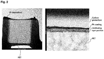
- a specimen of the laminate for TEM measurement was prepared using FIB. A FETEM STEM BF image of the prepared specimen is shown in Fig. 2 .
- the boundary between the antifouling layer and the carbon protective layer can be distinguished by the Pt coating layer which is observed relatively darker than the carbon compound. Further, a layer with contrast different from the Pt coating layer under the Pt coating layer was additionally observed, and the thickness of the layer was measured at about 50 nm, which is similar to the thickness of the antifouling layer. From this, it can be seen that the antifouling layer can exhibit a clear contrast with the PET layer which is a polymer substrate made of only a carbon compound. Further, in the TEM image, the boundary between the PET substrate and the antifouling layer was observed to be flat, and it can be clearly distinguished that the overall thickness of the layer is constant.
- EDS Energy Dispersive Spectrometer
- the profile of the Pt content measured in the antifouling layer is almost constant in the antifouling layer and is decreased in a stepwise manner in the end region of the antifouling layer. It can be seen that Pt is not simply diffused into the antifouling layer, but it has the effect of staining only the antifouling layer through a kind of reaction. This may be due to the reaction with PEDOT:PSS contained in the antifouling layer.
- An antistatic antifouling layer was formed to the target thickness of about 50 nm on a PET substrate using a composition containing polyurethane (PU) binder.
- a Pt coating layer was formed on the antistatic antifouling layer to a thickness of 10 nm and then a carbon protection was formed thereon to manufacture a laminate that is laminated in order of PET/PU/Pt/carbon protection.
- a specimen of the laminate for TEM measurement was prepared using FIB.
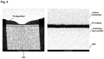
- a FETEM STEM BF image of the prepared specimen is shown in Fig. 4 .
- PEDOT:PSS diffuses the Pt of the Pt coating layer into the antifouling layer and at the same time, it induces the reaction with PEDOT:PSS, allowing the observation of the antifouling layer in the TEM image.
- the diffusion reaction can be assumed to be due to the ionic interaction between the negative charge of PEDOT:PSS and the positive charge of Pt (metal).
- Two specimens were prepared to the target thickness of 50 nm and 150 nm.
- Antistatic antifouling layers were formed to the target thickness of about 50 nm and 150 nm on PET substrates, respectively, using a composition containing 3 wt% of PEDOT:PSS conductive polymer and 97 wt% of polyurethane (PU) binder. Pt coating layers were formed on the antistatic antifouling layers to a thickness of 10 nm and then carbon protections were formed thereon to manufacture laminates that are laminated in order of PET/PEDOT:PSS-PU/Pt/carbon protection. Specimens of the laminates for TEM measurement were prepared using FIB.
- a TEM image of the prepared specimen is shown in Fig. 5 .
- the specimen target thickness of 50 nm was measured at about 25 nm, and the specimen target thickness of 150 nm was measured at about 60 nm.
- the measured thickness was measured to be thinner than the expected thickness. It can be expected that the specimen made in the laboratory is coated thinner than the target thickness. However, it was confirmed that the thickness tendency agrees with the thickness difference about three times.
Landscapes
- Chemical & Material Sciences (AREA)
- Life Sciences & Earth Sciences (AREA)
- Immunology (AREA)
- Pathology (AREA)
- Analytical Chemistry (AREA)
- Biochemistry (AREA)
- General Health & Medical Sciences (AREA)
- General Physics & Mathematics (AREA)
- Physics & Mathematics (AREA)
- Health & Medical Sciences (AREA)
- Engineering & Computer Science (AREA)
- Materials Engineering (AREA)
- Wood Science & Technology (AREA)
- Organic Chemistry (AREA)
- Laminated Bodies (AREA)
- Analysing Materials By The Use Of Radiation (AREA)
- Sampling And Sample Adjustment (AREA)
Abstract
Description
- The present application claims the benefits of priority to Korean Patent Application No.
10-2017-0167151, filed on December 07, 2017 - The present invention relates to a specimen used for analyzing shape of an antistatic antifouling layer and a method for manufacturing thereof, and more specifically, to a specimen useful for analyzing shape of an antistatic antifouling layer by using TEM and a method for manufacturing thereof.
- A polarizing plate protective film protects the surface of a product by sticking to a polarizing plate and a backlight unit in the LCD manufacturing process. As the polarizing plate protective film, a polyethylene terephthalate (PET) film is generally used. In order to prevent contamination of the film, an antifouling layer having a thickness of several tens of nanometers is coated thereon. Further, this protective film is removed from the process at the final stage of the LCD module production process. Defect occurs due to weak static electricity of about 1 kV to 5 kV generated when the film is peeled off, and the defect rate is known to be about 20%. Therefore, an antistatic antifouling layer made by mixing a conductive polymer such as poly(3,4-ethylenedioxythiophene)polystyrene sulfonate (PEDOT:PSS) with a binder such as polyurethane is coated on a PET film to prevent the defects caused by static electricity.
- The problem to be solved by the present invention is to provide a specimen that can more clearly analyze shape of an antistatic antifouling layer formed on a polymer substrate using TEM and a method for manufacturing thereof.
- Further, the present invention is to provide a method for analyzing shape of the antistatic antifouling layer formed on a polymer substrate using the specimen.
- In order to solve the above-mentioned problems, the present invention provides a specimen for analyzing shape of an antistatic antifouling layer comprising: a polymer substrate; an antistatic antifouling layer, which is formed on the polymer substrate and contains a conductive polymer; and a Pt (platinum) coating layer directly formed on the antistatic antifouling layer.
- According to one embodiment, the specimen may further comprise a carbon protective film on the Pt coating layer.
- Further, the present invention provides a method for manufacturing the specimen for analyzing shape of an antistatic antifouling layer, which comprises the following steps of:
- forming the antistatic antifouling layer containing a conductive polymer formed on the polymer substrate; and
- directly forming the Pt coating layer on the antistatic antifouling layer.
- According to one embodiment, the method may further comprise a step of forming the carbon protective film on the Pt coating layer.
- According to one embodiment, the conductive polymer may contain PEDOT:PSS.
- According to one embodiment, the antistatic antifouling layer may be made from a composition containing the conductive polymer of 2 wt% to 20 wt% and a polymer resin binder of 80 wt% to 98wt%.
- According to one embodiment, the thickness of the antistatic antifouling layer may be 30 nm to 200 nm.
- According to one embodiment, the thickness of the Pt coating layer may be 5 nm to 20 nm.
- Further, in order to solve another problem of the present invention, the present invention provides a method for analyzing shape of the antistatic antifouling layer using TEM to the specimen manufactured by the above-mentioned method.
- According to the present invention, directly coating Pt on the antistatic antifouling layer, which is formed on a polymer substrate and contains a conductive polymer, is resulted in the contrast difference between the polymer substrate layer and the antistatic antifouling layer due to the diffusion of Pt by the conductive polymer and the dyeing effect of the antifouling layer. This makes it possible to more clearly distinguish shape of the antistatic antifouling layer formed on the polymer substrate using TEM.
-
-
Fig. 1 is a FE-TEM image of a specimen including a PET/antifouling layer manufactured by the conventional method. -
Fig. 2 is a Field Emission Transmission Electron Microscopy (FETEM)-bright-field (BF) image of a specimen including a PET/polyurethane-PEDOT:PSS antifouling layer manufactured by the method according to the present invention. -
Figs. 3a and3b are the results of measuring Energy Dispersive Spectrometer (EDS), which analyzes the content of Pt contained in the specimen including PET/polyurethane-PEDOT:PSS antifouling layer manufactured by the method according to the present invention. -
Fig. 4 is a FETEM-BF image of a specimen including the antifouling layer formed with only polyurethane according to Comparative Example 2. -
Fig. 5 is a FETEM-BF image with antifouling layer thickness variation in the specimen including PET/polyurethane-PEDOT:PSS antifouling layer manufactured by the method according to the present invention. - Various changes in form and details may be made to the presently disclosed embodiment and thus should not be construed as being limited to the aspects set forth herein. The presently disclosed embodiment is not limited to the aspects described in the present description, and thus it should be understood that the presently disclosed embodiment includes every kind of variation example or alternative equivalent included in the spirit and scope of the presently disclosed embodiment. Also, while describing the aspects, detailed descriptions about related well-known functions or configurations that may diminish the clarity of the points of the aspects of the presently disclosed embodiment will be omitted.
- The present invention relates to a specimen useful for analyzing shape of an antistatic antifouling layer by using TEM and a method for manufacturing thereof.
- Herein, the term TEM should be understood to include transmission electron microscopes of all kinds, for example, all of Universal design TEM, Scanning transmission electron microscope (STEM), Field emission transmission electron microscope (FE-TEM) and the like.
- A polarizing plate protective film coated with an antifouling layer, which includes a conductive polymer and has an antistatic function, can exhibit a tendency to change the surface resistance depending on the thickness of the antifouling layer. In order to analyze to confirm the correlation between the thickness of the antifouling layer and the surface resistance, the thickness of the antistatic antifouling layer formed on the protective film should be clearly measured.
- However, in general, the thickness of the antifouling layer is about 50 nm, which is very thin, and both of the substrate and the antifouling layer are carbon compounds. Accordingly, there is a problem that it is difficult to observe the antifouling layer using an electron microscope due to small contrast range.
- In order to solve the above-mentioned problems, the present invention provides a specimen for analyzing shape of an antistatic antifouling layer comprising: a polymer substrate; an antistatic antifouling layer, which is formed on the polymer substrate and contains a conductive polymer; and a Pt coating layer directly formed on the antistatic antifouling layer.
- According to a preferred embodiment, the specimen may further comprise a carbon protective film on the Pt coating layer.
- Further, the present invention provides a method for manufacturing the specimen for analyzing shape of an antistatic antifouling layer, which comprises the following steps of:
- forming the antistatic antifouling layer containing a conductive polymer formed on the polymer substrate; and
- directly forming the Pt coating layer on the antistatic antifouling layer.
- According to the present invention, the antistatic antifouling layer and the substrate can be clearly distinguished by measuring the Transmission electron microscope (TEM) after coating the surface of the antistatic antifouling layer directly with Pt.
- In the present invention, the Pt coating may be applied by using techniques known in the art such as sputtering, but not particularly limited thereto.
- Further, the method of the present invention may further comprise a step of forming the carbon protective film on the Pt coating layer. The carbon protective film may be formed by using techniques known in the art such as a technique to draw an organic ink pen such as an oil-based pen on an area of interest, but not particularly limited thereto.
- In particular, in the case of using a focused ion beam (FIB) to manufacture a specimen for TEM analysis, it is preferred to form the carbon protective film on the Pt coating layer.
- In general, in the case of manufacturing a thin specimen of a polymer sample using an FIB (Focused Ion Beam), a carbon protective film has been formed and then the Pt coating has been pretreated to protect the polymer surface relatively weak against the ion beam. However, in this conventional method, there has been difficult to observe the thickness and shape of the antifouling layer formed on the polymer substrate since both the polymer substrate and the antifouling layer are made of carbon compounds and therefore, there is no contrast difference.
- In the method for manufacturing a TEM thin specimen of a polymer sample, Pt coating, which has been carried out after the formation of the carbon protective film (carbon protection), is directly performed on the antifouling layer, the present invention can obtain an effect that Pt is diffused and stained by the conductive polymer contained in the antifouling layer. This effect causes contrast between the Pt coating layer, the antifouling layer and the substrate layer to clearly distinguish the boundaries of the Pt coating layer, the antifouling layer and the substrate layer. Thus, the shape and thickness of the antifouling layer formed on the substrate can be more clearly measured.
- The antistatic antifouling layer may be formed by the method known in the art, but not particularly limited thereto. For example, it may be made from a composition containing the conductive polymer of 2 wt% to 20 wt% and a polymer resin binder of 80 wt% to 98 wt%, and if desired, various additives may be further included. The content of the conductive polymer may be 2 wt% to 20 wt%, preferably 2 wt% to 15 wt%, more preferably 2 wt% to 10 wt%, based on the total weight of the composition for forming an antifouling layer.
- According to one embodiment, the conductive polymer may be at least one selected from the group consisting of polythiophene-based, polypyrrole-based, polystyrene-based and polyaniline-based polymers, and preferably, it may be polythiophene-based conductive polymer or polystyrene-based conductive polymer.
- In general, as the conductive polymer used for the antistatic antifouling layer, PEDOT:PSS, which is a conductive polymer doped with polystyrene sulfonic acid (PSS) as a dopant in an aqueous dispersion in which polyethylene disocythiophene (PEDOT), can be mainly used, and it can be confirmed that the surface resistance is lowered by applying PEDOT:PSS to the antistatic antifouling layer. However, it is not limited thereto, and the known conductive polymers can be used without limitation.
- As shown in the following
Chemical Formula 1, the PEDOT:PSS is a polymer in which two ionomers are combined, and the sulfonyl group of the sulfonated polystyrene has a negative charge and the polythiophene part of the PEDOT has a positive charge. Therefore, the PEDOT:PSS can exhibit a high electrical conductivity of around 1000 S/cm by only a simple doping.

- Further, the polymer resin binder may contain at least one polymer resin selected from the group consisting of polyester-based, polyurethane-based, acryl resin-based, polyvinyl-based and polyolefin-based resins, preferably polyurethane-based polymer.
- The polymer substrate used as a protective film may contain at least one polymer selected from the group consisting of polyester, polystyrene, polyimide, polyamide, polysulfonate, polycarbonate, polyacrylate, polyethylene, polypropylene and the like.
- According to one embodiment, the thickness of the antistatic antifouling layer may be 30 nm to 200 nm, preferably 30 nm to 150 nm.
- According to one embodiment, the Pt coating layer may be coated to the thickness of 5 nm to 20 nm, preferably 5 nm to 15 nm, more preferably 5 nm to 10 nm.
- In the present invention, as the Pt is directly coated on the antistatic antifouling layer containing the conductive polymer, it is diffused into the antifouling layer contained in the Pt coating layer, and the pretreatment effect such as dyeing in the electron microscopic pretreatment technique is applied to induce the contrast difference between the substrate and the antifouling layer. For example, the ionic interaction between the negative charge of the PEDOT:PSS that is a conductive polymer in the antifouling layer and the positive charge of the Pt metal generated during the Pt coating may occur, and the Pt may diffuse into the antifouling layer, resulting in the contrast difference with the substrate.
- According to one embodiment, the content of the Pt contained in the antistatic antifouling layer can be distributed in a substantially constant amount in the entire region of the antifouling layer regardless of the distance from the Pt coating layer. Analysis of the Pt content in the antifouling layer revealed that the Pt content in the end region of the antifouling layer decreased in a stepwise manner while maintaining almost constant content in the entire region of the antifouling layer unlike the general diffusion profile showing a tail shape. This may indicate that the Pt is not only diffused into the antifouling layer but can also be an effect of staining only the antifouling layer through a kind of reaction.
- Hereinafter, the working examples of the present invention will be explained in detail so that an ordinary skilled in the art can easily carry out the present invention. The accompanying examples are provided for illustration only and should not be construed as limiting the scope of the invention.
- *
- Pt coating system (Hitachi E-1030)
- In order to protect the surface of a sample and reduce the charging phenomenon, the coating thickness was estimated to be 10 nm by sputtering for 100 sec.
- A carbon protective layer was formed by applying oil on the area of interest to be observed by using an oil-based pen containing an organic ink.
- Dual beam focused ion beam (FEI Helios450F1)
- It was used to make a thin slice of 100 nm thick or less. Ion beam current was reduced to 9.3 nA and 80 pA and processed sequentially.
- TEM (FE-STEM, TITIAN G2 80-200 Chemi-STEM)
- It was used for observing an antifouling layer (Acceleration voltage: 80-200 kV, Resolution: point of resolution (240 pm), Energy spread: 0.8 Ev).
- An antistatic antifouling layer was formed to the target thickness of about 50 nm on a PET substrate using a composition containing 3 wt% of PEDOT:PSS conductive polymer and 97 wt% of polyurethane (PU) binder. After carbon protection was performed to protect the surface of the antistatic antifouling layer, a Pt coating layer was formed on the carbon protective layer to a thickness of 10 nm to manufacture a laminate that is laminated in order of PET/PEDOT:PSS-PU/carbon protection/Pt. A specimen of the laminate for TEM measurement was prepared using FIB. A FETEM STEM BF image of the prepared specimen is shown in
Fig. 1 . - In the case of the specimen pretreated as described above, since the antifouling layer is a carbon-based thin layer and the PET and the carbon protective layer are also carbon-based materials, it is difficult to distinguish the antifouling layer because there is no contrast difference on the TEM image.
- An antistatic antifouling layer was formed to the target thickness of about 50 nm on a PET substrate using a composition containing 3 wt% of PEDOT:PSS conductive polymer and 97 wt% of polyurethane (PU) binder. A Pt coating layer was formed on the antistatic antifouling layer to a thickness of 10 nm and then a carbon protection was formed thereon to manufacture a laminate that is laminated in order of PET/PEDOT:PSS-PU/Pt/carbon protection. A specimen of the laminate for TEM measurement was prepared using FIB. A FETEM STEM BF image of the prepared specimen is shown in
Fig. 2 . - As can be seen from the results of
Fig. 2 , the boundary between the antifouling layer and the carbon protective layer can be distinguished by the Pt coating layer which is observed relatively darker than the carbon compound. Further, a layer with contrast different from the Pt coating layer under the Pt coating layer was additionally observed, and the thickness of the layer was measured at about 50 nm, which is similar to the thickness of the antifouling layer. From this, it can be seen that the antifouling layer can exhibit a clear contrast with the PET layer which is a polymer substrate made of only a carbon compound. Further, in the TEM image, the boundary between the PET substrate and the antifouling layer was observed to be flat, and it can be clearly distinguished that the overall thickness of the layer is constant. - Accordingly, Energy Dispersive Spectrometer (EDS) component analysis of the antifouling layer was performed to analyze the Pt content in the antifouling layer. The analysis results are shown in
Figs. 3a and3b . As a result of the above EDS analysis, Pt was detected inside the antifouling layer, and as a result of the line scan, as shown inFig. 3b , a constant amount of Pt was detected in the antifouling layer regardless of the distance from the Pt coating layer. From the above results, it can be seen that Pt of the Pt coating layer is diffused into the antifouling layer, and due to the diffusion of Pt, the antifouling layer is provided with a relatively dark contrast so that the antifouling layer formed on the polymer substrate can be clearly observed. - Further, as one uniqueness of the present invention, in contrast to the typical diffusion characteristics with a tail shape whose content is gradually decreased according to the distance, the profile of the Pt content measured in the antifouling layer is almost constant in the antifouling layer and is decreased in a stepwise manner in the end region of the antifouling layer. It can be seen that Pt is not simply diffused into the antifouling layer, but it has the effect of staining only the antifouling layer through a kind of reaction. This may be due to the reaction with PEDOT:PSS contained in the antifouling layer.
- An antistatic antifouling layer was formed to the target thickness of about 50 nm on a PET substrate using a composition containing polyurethane (PU) binder. A Pt coating layer was formed on the antistatic antifouling layer to a thickness of 10 nm and then a carbon protection was formed thereon to manufacture a laminate that is laminated in order of PET/PU/Pt/carbon protection. A specimen of the laminate for TEM measurement was prepared using FIB. A FETEM STEM BF image of the prepared specimen is shown in
Fig. 4 . - As shown in
Fig. 4 , in the specimen obtained by coating only polyurethane (PU) to the same thickness without PEDOT:PSS conductive polymer as described above, no antifouling layer was observed and only the Pt coating layer was confirmed. - Thus, it can be seen that PEDOT:PSS diffuses the Pt of the Pt coating layer into the antifouling layer and at the same time, it induces the reaction with PEDOT:PSS, allowing the observation of the antifouling layer in the TEM image. The diffusion reaction can be assumed to be due to the ionic interaction between the negative charge of PEDOT:PSS and the positive charge of Pt (metal).
- Two specimens were prepared to the target thickness of 50 nm and 150 nm.
- Antistatic antifouling layers were formed to the target thickness of about 50 nm and 150 nm on PET substrates, respectively, using a composition containing 3 wt% of PEDOT:PSS conductive polymer and 97 wt% of polyurethane (PU) binder. Pt coating layers were formed on the antistatic antifouling layers to a thickness of 10 nm and then carbon protections were formed thereon to manufacture laminates that are laminated in order of PET/PEDOT:PSS-PU/Pt/carbon protection. Specimens of the laminates for TEM measurement were prepared using FIB.
- A TEM image of the prepared specimen is shown in
Fig. 5 . The specimen target thickness of 50 nm was measured at about 25 nm, and the specimen target thickness of 150 nm was measured at about 60 nm. The measured thickness was measured to be thinner than the expected thickness. It can be expected that the specimen made in the laboratory is coated thinner than the target thickness. However, it was confirmed that the thickness tendency agrees with the thickness difference about three times. - From the above results, it can be seen that not only the antifouling layer can be clearly observed in the TEM image through the simple pretreatment of the Pt coating but also the Pt of the Pt coating layer is diffused into the antifouling layer by the conductive polymer PEDOT:PSS and reacted.
- It should be understood that those skilled in the art can carry out other modifications without changing its technical spirit or essential features. Therefore, the above-described embodiment of the present invention is merely exemplary in all aspects and should not be construed to be limited, and it should be understood that the scope of the present invention is defined by the following claims and the meanings and ranges of the claims and all modifications and changed forms derived from their equivalents pertain to the scope of the present invention.
Claims (9)
- A specimen for analyzing shape of an antistatic antifouling layer comprising:a polymer substrate;an antistatic antifouling layer, which is formed on the polymer substrate and contains a conductive polymer; anda Pt coating layer directly formed on the antistatic antifouling layer.
- The specimen for analyzing shape of an antistatic antifouling layer according to claim 1, further comprising a carbon protective film on the Pt coating layer.
- The specimen for analyzing shape of an antistatic antifouling layer according to claim 1, wherein the conductive polymer contains PEDOT:PSS.
- The specimen for analyzing shape of an antistatic antifouling layer according to claim 1, wherein the antistatic antifouling layer is made from a composition containing the conductive polymer in an amount of 2 wt% to 20 wt% and a polymer resin binder in an amount of 80 wt% to 98 wt%.
- The specimen for analyzing shape of an antistatic antifouling layer according to claim 1, wherein a thickness of the antistatic antifouling layer is 30 nm to 200 nm.
- The specimen for analyzing shape of an antistatic antifouling layer according to claim 1, wherein a thickness of the Pt coating layer is 5 nm to 20 nm.
- A method for manufacturing a specimen for analyzing shape of an antistatic antifouling layer comprising:forming an antistatic antifouling layer containing a conductive polymer formed on a polymer substrate; anddirectly forming a Pt coating layer on the antistatic antifouling layer.
- The method for manufacturing a specimen for analyzing shape of an antistatic antifouling layer according to claim 7, further comprising forming a carbon protective film on the Pt coating layer.
- A method for analyzing shape of an antistatic antifouling layer comprising analyzing the specimen according to any one of claim 1 to claim 6 using TEM.
Applications Claiming Priority (2)
| Application Number | Priority Date | Filing Date | Title |
|---|---|---|---|
| KR1020170167151A KR102140857B1 (en) | 2017-12-07 | 2017-12-07 | A specimen for analyzing antistatic antifouling layer and a method for preparing same |
| PCT/KR2018/015232 WO2019112284A1 (en) | 2017-12-07 | 2018-12-04 | Specimen for analyzing shape of antistatic antifouling layer and method for preparing same |
Publications (3)
| Publication Number | Publication Date |
|---|---|
| EP3722778A1 true EP3722778A1 (en) | 2020-10-14 |
| EP3722778A4 EP3722778A4 (en) | 2021-01-13 |
| EP3722778B1 EP3722778B1 (en) | 2023-05-10 |
Family
ID=66750231
Family Applications (1)
| Application Number | Title | Priority Date | Filing Date |
|---|---|---|---|
| EP18885317.0A Active EP3722778B1 (en) | 2017-12-07 | 2018-12-04 | Specimen for analyzing shape of antistatic antifouling layer and method for preparing same |
Country Status (6)
| Country | Link |
|---|---|
| US (1) | US11262279B2 (en) |
| EP (1) | EP3722778B1 (en) |
| JP (1) | JP6988055B2 (en) |
| KR (1) | KR102140857B1 (en) |
| CN (1) | CN111051845B (en) |
| WO (1) | WO2019112284A1 (en) |
Families Citing this family (2)
| Publication number | Priority date | Publication date | Assignee | Title |
|---|---|---|---|---|
| WO2023223521A1 (en) * | 2022-05-19 | 2023-11-23 | 地方独立行政法人神奈川県立産業技術総合研究所 | Embedding and fixation composition for improving visibility in observation using electron microscope or the like, and observation method using same |
| KR20250070819A (en) | 2023-11-14 | 2025-05-21 | 한국에너지기술연구원 | Method of producing large-area samples for transmission electron microscopy to analyzing property measurement of membrane electrode assemblies in fuel cell |
Family Cites Families (26)
| Publication number | Priority date | Publication date | Assignee | Title |
|---|---|---|---|---|
| JPH05223755A (en) | 1992-02-18 | 1993-08-31 | Matsushita Electric Ind Co Ltd | Observation method for layered film with transparent electron microscope |
| KR100227825B1 (en) | 1996-09-19 | 1999-11-01 | 윤종용 | Transmission electron microscopy (TEM) sample preparation method |
| JP2001121273A (en) * | 1999-10-22 | 2001-05-08 | Printing Bureau Ministry Of Finance Japan | Method for preparing cross-section samples of paper and printed matter |
| JP2001316595A (en) | 2000-05-10 | 2001-11-16 | Kawamura Inst Of Chem Res | Composite formed product of electroconductive resin, and method for producing the same |
| JP4759955B2 (en) | 2003-08-28 | 2011-08-31 | 住友化学株式会社 | Method for producing antistatic plate having antiglare property and antistatic plate obtained thereby |
| JP4292296B2 (en) | 2004-07-28 | 2009-07-08 | 国立大学法人 大分大学 | Electron staining method for samples for transmission electron microscope observation. |
| KR100738317B1 (en) * | 2005-11-16 | 2007-07-12 | 주식회사 에이스 디지텍 | Manufacturing method of antistatic high resolution anti-glare optical device and antistatic high resolution anti-glare optical device using same |
| KR200413739Y1 (en) * | 2005-12-07 | 2006-04-13 | 임진석 | Laminated sheet with anti-adhesion function and self-cleaning function |
| KR100789239B1 (en) * | 2005-12-30 | 2008-01-02 | 주식회사 엘지화학 | Surface protection film for optical members |
| KR100937935B1 (en) | 2008-05-20 | 2010-01-21 | 강원대학교산학협력단 | Method of measuring thickness of polymer resin insulator film on bonding wire surface |
| JP5533857B2 (en) * | 2009-04-10 | 2014-06-25 | コニカミノルタ株式会社 | Optical film, polarizing plate and liquid crystal display device using the same |
| SG182593A1 (en) * | 2010-01-27 | 2012-08-30 | Teijin Ltd | Film |
| WO2011140658A1 (en) * | 2010-05-12 | 2011-11-17 | The Governing Council Of The University Of Toronto | Method of producing electrically conductive polymer and cellulose nanocomposites |
| JP2012202834A (en) | 2011-03-25 | 2012-10-22 | Tokyo Electric Power Co Inc:The | Observation method for microstructure of polymeric material |
| TWI530707B (en) | 2011-05-16 | 2016-04-21 | 大日本印刷股份有限公司 | Method for manufacturing anti-reflection film, anti-reflection film, polarizing plate, and image display device |
| CN102504485B (en) | 2011-10-20 | 2013-11-06 | 北京工业大学 | Conducting resin for scanning electronic microscope and preparation method thereof |
| JP5974709B2 (en) | 2012-07-26 | 2016-08-23 | 大日本印刷株式会社 | Anti-glare film, polarizing plate and image display device |
| US9505935B2 (en) * | 2012-09-27 | 2016-11-29 | Shin-Etsu Polymer Co., Ltd. | Antistatic release agent, antistatic release coated film and antistatic release base material |
| CN103808540B (en) * | 2012-11-08 | 2017-02-15 | 中芯国际集成电路制造(上海)有限公司 | Transmission electron microscope sample preparation method |
| JP6236246B2 (en) | 2013-07-31 | 2017-11-22 | 日東電工株式会社 | Adhesive sheet and optical member |
| WO2015147195A1 (en) * | 2014-03-27 | 2015-10-01 | リンテック株式会社 | Antifouling sheet and method for producing same |
| JP6405883B2 (en) * | 2014-10-21 | 2018-10-17 | 大日本印刷株式会社 | LAMINATE, CONDUCTIVE LAMINATE, AND TOUCH PANEL |
| KR102639383B1 (en) * | 2014-12-26 | 2024-02-21 | 스미또모 가가꾸 가부시키가이샤 | Anti-static polarizing plate, anti-static polarizing plate with adhesive layer, and optical laminate |
| JP2017119753A (en) * | 2015-12-28 | 2017-07-06 | 日東電工株式会社 | Surface protective film, method for manufacturing surface protective film, and optical member |
| KR101686386B1 (en) | 2016-07-20 | 2016-12-13 | 인천대학교 산학협력단 | 3d conductive coating method for clear sem measurement |
| KR101850939B1 (en) | 2016-09-28 | 2018-04-20 | 부경대학교 산학협력단 | Method for preparing micro-nano structures using nano membrane and micro-nano structures prepared thereby |
-
2017
- 2017-12-07 KR KR1020170167151A patent/KR102140857B1/en active Active
-
2018
- 2018-12-04 US US16/643,717 patent/US11262279B2/en active Active
- 2018-12-04 EP EP18885317.0A patent/EP3722778B1/en active Active
- 2018-12-04 CN CN201880054876.0A patent/CN111051845B/en active Active
- 2018-12-04 WO PCT/KR2018/015232 patent/WO2019112284A1/en not_active Ceased
- 2018-12-04 JP JP2020509013A patent/JP6988055B2/en active Active
Also Published As
| Publication number | Publication date |
|---|---|
| CN111051845B (en) | 2023-01-24 |
| EP3722778A4 (en) | 2021-01-13 |
| WO2019112284A1 (en) | 2019-06-13 |
| US11262279B2 (en) | 2022-03-01 |
| US20200209116A1 (en) | 2020-07-02 |
| EP3722778B1 (en) | 2023-05-10 |
| KR102140857B1 (en) | 2020-08-03 |
| CN111051845A (en) | 2020-04-21 |
| JP6988055B2 (en) | 2022-01-05 |
| JP2020531813A (en) | 2020-11-05 |
| KR20190067330A (en) | 2019-06-17 |
Similar Documents
| Publication | Publication Date | Title |
|---|---|---|
| Dixit et al. | Catalyst layer ink interactions that affect coatability | |
| EP3078962B1 (en) | Liquid medium for preventing charge-up in electron microscope and method of observing sample using the same | |
| Arimoto et al. | Development of in situ scanning electron microscope system for real time observation of metal deposition from ionic liquid | |
| Madl et al. | Vapor phase polymerization of poly (3, 4-ethylenedioxythiophene) on flexible substrates for enhanced transparent electrodes | |
| US11262279B2 (en) | Specimen for analyzing shape of antistatic antifouling layer and method for preparing same | |
| Bülter et al. | In situ quantification of the swelling of graphite composite electrodes by scanning electrochemical microscopy | |
| Skaja et al. | Avalanche‐Discharge‐Induced Electrical Forming in Tantalum Oxide‐Based Metal–Insulator–Metal Structures | |
| US20130130056A1 (en) | Corrosion-protective wax composition containing polyaniline in a doped form and a liquid paraffin | |
| Singer et al. | Influence of the slurry composition on thin-film components for the wet coating process of sulfide-based all-solid-state batteries | |
| EP2569351A1 (en) | Method of producing electrically conductive polymer and cellulose nanocomposites | |
| Ravati et al. | Phase identification and interfacial transitions in ternary polymer blends by ToF-SIMS | |
| Liu et al. | Comparing build architecture and electrolyte of ITO-free flexible patterned organic screen-printed ECDs based on a novel PEDOT: PSS compound film post-treated with strong and weak organic acids | |
| Kang et al. | A polyaniline/polyvinyl acetate composite film electrode for highly sensitive electrochemical sensing of pH | |
| Eswara-Moorthy et al. | An in situ SEM-FIB-based method for contrast enhancement and tomographic reconstruction for structural quantification of porous carbon electrodes | |
| Singer et al. | Drying Process of Sulfide‐Based All‐Solid‐State Battery Components—Investigation on Adhesion Strength and Microstructural Changes | |
| Yu et al. | In situ characterization of hydrated proteins in water by SALVI and ToF-SIMS | |
| Guanggui et al. | Study on the preparation and multiproperties of the polypyrrole films doped with different ions | |
| Yamamoto et al. | Blocking ion diffusion and minimizing electron charging in solid electrolytes under electron-beam irradiation for transmission electron microscopy analysis | |
| Orisekeh et al. | Mechanical properties of polyvinylpyrrolidone/polyvinyl alcohol‐based solid electrolytes | |
| Serantoni et al. | FIB-SIMS investigation of carbazole-based polymer and copolymers electrocoated onto carbon fibers, and an AFM morphological study | |
| Zankowski et al. | Chemical staining for fundamental studies and optimization of binders in Li-ion battery negative electrodes | |
| Bloomfield et al. | Classification of ToF-SIMS detected chemicals causing nearly 1000 automotive paint craters | |
| Ragusano et al. | Temperature-assisted high-energy-per-atom argon cluster SIMS of layered hybrid nanomaterials | |
| Geng et al. | Morphology observation of latex particles with scanning transmission electron microscopy by a hydroxyethyl cellulose embedding combined with RuO4 staining method | |
| Kim et al. | Highly conductive and transparent Ag NWs/alcohol based PEDOT: PSS− PPGA hybrid film with improved water resistance |
Legal Events
| Date | Code | Title | Description |
|---|---|---|---|
| STAA | Information on the status of an ep patent application or granted ep patent |
Free format text: STATUS: THE INTERNATIONAL PUBLICATION HAS BEEN MADE |
|
| PUAI | Public reference made under article 153(3) epc to a published international application that has entered the european phase |
Free format text: ORIGINAL CODE: 0009012 |
|
| STAA | Information on the status of an ep patent application or granted ep patent |
Free format text: STATUS: REQUEST FOR EXAMINATION WAS MADE |
|
| 17P | Request for examination filed |
Effective date: 20200212 |
|
| AK | Designated contracting states |
Kind code of ref document: A1 Designated state(s): AL AT BE BG CH CY CZ DE DK EE ES FI FR GB GR HR HU IE IS IT LI LT LU LV MC MK MT NL NO PL PT RO RS SE SI SK SM TR |
|
| AX | Request for extension of the european patent |
Extension state: BA ME |
|
| A4 | Supplementary search report drawn up and despatched |
Effective date: 20201214 |
|
| RIC1 | Information provided on ipc code assigned before grant |
Ipc: C09D 5/16 20060101ALI20201208BHEP Ipc: G01N 1/28 20060101AFI20201208BHEP Ipc: C09D 5/24 20060101ALI20201208BHEP |
|
| DAV | Request for validation of the european patent (deleted) | ||
| DAX | Request for extension of the european patent (deleted) | ||
| GRAP | Despatch of communication of intention to grant a patent |
Free format text: ORIGINAL CODE: EPIDOSNIGR1 |
|
| STAA | Information on the status of an ep patent application or granted ep patent |
Free format text: STATUS: GRANT OF PATENT IS INTENDED |
|
| INTG | Intention to grant announced |
Effective date: 20230110 |
|
| GRAS | Grant fee paid |
Free format text: ORIGINAL CODE: EPIDOSNIGR3 |
|
| GRAA | (expected) grant |
Free format text: ORIGINAL CODE: 0009210 |
|
| STAA | Information on the status of an ep patent application or granted ep patent |
Free format text: STATUS: THE PATENT HAS BEEN GRANTED |
|
| AK | Designated contracting states |
Kind code of ref document: B1 Designated state(s): AL AT BE BG CH CY CZ DE DK EE ES FI FR GB GR HR HU IE IS IT LI LT LU LV MC MK MT NL NO PL PT RO RS SE SI SK SM TR |
|
| REG | Reference to a national code |
Ref country code: GB Ref legal event code: FG4D |
|
| REG | Reference to a national code |
Ref country code: AT Ref legal event code: REF Ref document number: 1567137 Country of ref document: AT Kind code of ref document: T Effective date: 20230515 Ref country code: CH Ref legal event code: EP |
|
| REG | Reference to a national code |
Ref country code: DE Ref legal event code: R096 Ref document number: 602018049838 Country of ref document: DE |
|
| REG | Reference to a national code |
Ref country code: IE Ref legal event code: FG4D |
|
| REG | Reference to a national code |
Ref country code: LT Ref legal event code: MG9D |
|
| REG | Reference to a national code |
Ref country code: NL Ref legal event code: MP Effective date: 20230510 |
|
| REG | Reference to a national code |
Ref country code: AT Ref legal event code: MK05 Ref document number: 1567137 Country of ref document: AT Kind code of ref document: T Effective date: 20230510 |
|
| PG25 | Lapsed in a contracting state [announced via postgrant information from national office to epo] |
Ref country code: SE Free format text: LAPSE BECAUSE OF FAILURE TO SUBMIT A TRANSLATION OF THE DESCRIPTION OR TO PAY THE FEE WITHIN THE PRESCRIBED TIME-LIMIT Effective date: 20230510 Ref country code: PT Free format text: LAPSE BECAUSE OF FAILURE TO SUBMIT A TRANSLATION OF THE DESCRIPTION OR TO PAY THE FEE WITHIN THE PRESCRIBED TIME-LIMIT Effective date: 20230911 Ref country code: NO Free format text: LAPSE BECAUSE OF FAILURE TO SUBMIT A TRANSLATION OF THE DESCRIPTION OR TO PAY THE FEE WITHIN THE PRESCRIBED TIME-LIMIT Effective date: 20230810 Ref country code: NL Free format text: LAPSE BECAUSE OF FAILURE TO SUBMIT A TRANSLATION OF THE DESCRIPTION OR TO PAY THE FEE WITHIN THE PRESCRIBED TIME-LIMIT Effective date: 20230510 Ref country code: ES Free format text: LAPSE BECAUSE OF FAILURE TO SUBMIT A TRANSLATION OF THE DESCRIPTION OR TO PAY THE FEE WITHIN THE PRESCRIBED TIME-LIMIT Effective date: 20230510 Ref country code: AT Free format text: LAPSE BECAUSE OF FAILURE TO SUBMIT A TRANSLATION OF THE DESCRIPTION OR TO PAY THE FEE WITHIN THE PRESCRIBED TIME-LIMIT Effective date: 20230510 |
|
| PG25 | Lapsed in a contracting state [announced via postgrant information from national office to epo] |
Ref country code: RS Free format text: LAPSE BECAUSE OF FAILURE TO SUBMIT A TRANSLATION OF THE DESCRIPTION OR TO PAY THE FEE WITHIN THE PRESCRIBED TIME-LIMIT Effective date: 20230510 Ref country code: PL Free format text: LAPSE BECAUSE OF FAILURE TO SUBMIT A TRANSLATION OF THE DESCRIPTION OR TO PAY THE FEE WITHIN THE PRESCRIBED TIME-LIMIT Effective date: 20230510 Ref country code: LV Free format text: LAPSE BECAUSE OF FAILURE TO SUBMIT A TRANSLATION OF THE DESCRIPTION OR TO PAY THE FEE WITHIN THE PRESCRIBED TIME-LIMIT Effective date: 20230510 Ref country code: LT Free format text: LAPSE BECAUSE OF FAILURE TO SUBMIT A TRANSLATION OF THE DESCRIPTION OR TO PAY THE FEE WITHIN THE PRESCRIBED TIME-LIMIT Effective date: 20230510 Ref country code: IS Free format text: LAPSE BECAUSE OF FAILURE TO SUBMIT A TRANSLATION OF THE DESCRIPTION OR TO PAY THE FEE WITHIN THE PRESCRIBED TIME-LIMIT Effective date: 20230910 Ref country code: HR Free format text: LAPSE BECAUSE OF FAILURE TO SUBMIT A TRANSLATION OF THE DESCRIPTION OR TO PAY THE FEE WITHIN THE PRESCRIBED TIME-LIMIT Effective date: 20230510 Ref country code: GR Free format text: LAPSE BECAUSE OF FAILURE TO SUBMIT A TRANSLATION OF THE DESCRIPTION OR TO PAY THE FEE WITHIN THE PRESCRIBED TIME-LIMIT Effective date: 20230811 |
|
| PG25 | Lapsed in a contracting state [announced via postgrant information from national office to epo] |
Ref country code: FI Free format text: LAPSE BECAUSE OF FAILURE TO SUBMIT A TRANSLATION OF THE DESCRIPTION OR TO PAY THE FEE WITHIN THE PRESCRIBED TIME-LIMIT Effective date: 20230510 |
|
| PG25 | Lapsed in a contracting state [announced via postgrant information from national office to epo] |
Ref country code: SK Free format text: LAPSE BECAUSE OF FAILURE TO SUBMIT A TRANSLATION OF THE DESCRIPTION OR TO PAY THE FEE WITHIN THE PRESCRIBED TIME-LIMIT Effective date: 20230510 |
|
| PG25 | Lapsed in a contracting state [announced via postgrant information from national office to epo] |
Ref country code: SM Free format text: LAPSE BECAUSE OF FAILURE TO SUBMIT A TRANSLATION OF THE DESCRIPTION OR TO PAY THE FEE WITHIN THE PRESCRIBED TIME-LIMIT Effective date: 20230510 Ref country code: SK Free format text: LAPSE BECAUSE OF FAILURE TO SUBMIT A TRANSLATION OF THE DESCRIPTION OR TO PAY THE FEE WITHIN THE PRESCRIBED TIME-LIMIT Effective date: 20230510 Ref country code: RO Free format text: LAPSE BECAUSE OF FAILURE TO SUBMIT A TRANSLATION OF THE DESCRIPTION OR TO PAY THE FEE WITHIN THE PRESCRIBED TIME-LIMIT Effective date: 20230510 Ref country code: EE Free format text: LAPSE BECAUSE OF FAILURE TO SUBMIT A TRANSLATION OF THE DESCRIPTION OR TO PAY THE FEE WITHIN THE PRESCRIBED TIME-LIMIT Effective date: 20230510 Ref country code: DK Free format text: LAPSE BECAUSE OF FAILURE TO SUBMIT A TRANSLATION OF THE DESCRIPTION OR TO PAY THE FEE WITHIN THE PRESCRIBED TIME-LIMIT Effective date: 20230510 Ref country code: CZ Free format text: LAPSE BECAUSE OF FAILURE TO SUBMIT A TRANSLATION OF THE DESCRIPTION OR TO PAY THE FEE WITHIN THE PRESCRIBED TIME-LIMIT Effective date: 20230510 |
|
| REG | Reference to a national code |
Ref country code: DE Ref legal event code: R097 Ref document number: 602018049838 Country of ref document: DE |
|
| PLBE | No opposition filed within time limit |
Free format text: ORIGINAL CODE: 0009261 |
|
| STAA | Information on the status of an ep patent application or granted ep patent |
Free format text: STATUS: NO OPPOSITION FILED WITHIN TIME LIMIT |
|
| 26N | No opposition filed |
Effective date: 20240213 |
|
| PG25 | Lapsed in a contracting state [announced via postgrant information from national office to epo] |
Ref country code: SI Free format text: LAPSE BECAUSE OF FAILURE TO SUBMIT A TRANSLATION OF THE DESCRIPTION OR TO PAY THE FEE WITHIN THE PRESCRIBED TIME-LIMIT Effective date: 20230510 |
|
| PG25 | Lapsed in a contracting state [announced via postgrant information from national office to epo] |
Ref country code: SI Free format text: LAPSE BECAUSE OF FAILURE TO SUBMIT A TRANSLATION OF THE DESCRIPTION OR TO PAY THE FEE WITHIN THE PRESCRIBED TIME-LIMIT Effective date: 20230510 Ref country code: IT Free format text: LAPSE BECAUSE OF FAILURE TO SUBMIT A TRANSLATION OF THE DESCRIPTION OR TO PAY THE FEE WITHIN THE PRESCRIBED TIME-LIMIT Effective date: 20230510 |
|
| REG | Reference to a national code |
Ref country code: CH Ref legal event code: PL |
|
| PG25 | Lapsed in a contracting state [announced via postgrant information from national office to epo] |
Ref country code: LU Free format text: LAPSE BECAUSE OF NON-PAYMENT OF DUE FEES Effective date: 20231204 |
|
| PG25 | Lapsed in a contracting state [announced via postgrant information from national office to epo] |
Ref country code: MC Free format text: LAPSE BECAUSE OF FAILURE TO SUBMIT A TRANSLATION OF THE DESCRIPTION OR TO PAY THE FEE WITHIN THE PRESCRIBED TIME-LIMIT Effective date: 20230510 |
|
| REG | Reference to a national code |
Ref country code: BE Ref legal event code: MM Effective date: 20231231 |
|
| PG25 | Lapsed in a contracting state [announced via postgrant information from national office to epo] |
Ref country code: MC Free format text: LAPSE BECAUSE OF FAILURE TO SUBMIT A TRANSLATION OF THE DESCRIPTION OR TO PAY THE FEE WITHIN THE PRESCRIBED TIME-LIMIT Effective date: 20230510 Ref country code: LU Free format text: LAPSE BECAUSE OF NON-PAYMENT OF DUE FEES Effective date: 20231204 |
|
| REG | Reference to a national code |
Ref country code: IE Ref legal event code: MM4A |
|
| PG25 | Lapsed in a contracting state [announced via postgrant information from national office to epo] |
Ref country code: IE Free format text: LAPSE BECAUSE OF NON-PAYMENT OF DUE FEES Effective date: 20231204 |
|
| PG25 | Lapsed in a contracting state [announced via postgrant information from national office to epo] |
Ref country code: BE Free format text: LAPSE BECAUSE OF NON-PAYMENT OF DUE FEES Effective date: 20231231 |
|
| PG25 | Lapsed in a contracting state [announced via postgrant information from national office to epo] |
Ref country code: CH Free format text: LAPSE BECAUSE OF NON-PAYMENT OF DUE FEES Effective date: 20231231 |
|
| PG25 | Lapsed in a contracting state [announced via postgrant information from national office to epo] |
Ref country code: IE Free format text: LAPSE BECAUSE OF NON-PAYMENT OF DUE FEES Effective date: 20231204 Ref country code: CH Free format text: LAPSE BECAUSE OF NON-PAYMENT OF DUE FEES Effective date: 20231231 Ref country code: BE Free format text: LAPSE BECAUSE OF NON-PAYMENT OF DUE FEES Effective date: 20231231 |
|
| PG25 | Lapsed in a contracting state [announced via postgrant information from national office to epo] |
Ref country code: BG Free format text: LAPSE BECAUSE OF FAILURE TO SUBMIT A TRANSLATION OF THE DESCRIPTION OR TO PAY THE FEE WITHIN THE PRESCRIBED TIME-LIMIT Effective date: 20230510 |
|
| PG25 | Lapsed in a contracting state [announced via postgrant information from national office to epo] |
Ref country code: BG Free format text: LAPSE BECAUSE OF FAILURE TO SUBMIT A TRANSLATION OF THE DESCRIPTION OR TO PAY THE FEE WITHIN THE PRESCRIBED TIME-LIMIT Effective date: 20230510 |
|
| PG25 | Lapsed in a contracting state [announced via postgrant information from national office to epo] |
Ref country code: CY Free format text: LAPSE BECAUSE OF FAILURE TO SUBMIT A TRANSLATION OF THE DESCRIPTION OR TO PAY THE FEE WITHIN THE PRESCRIBED TIME-LIMIT; INVALID AB INITIO Effective date: 20181204 |
|
| PG25 | Lapsed in a contracting state [announced via postgrant information from national office to epo] |
Ref country code: HU Free format text: LAPSE BECAUSE OF FAILURE TO SUBMIT A TRANSLATION OF THE DESCRIPTION OR TO PAY THE FEE WITHIN THE PRESCRIBED TIME-LIMIT; INVALID AB INITIO Effective date: 20181204 |
|
| PG25 | Lapsed in a contracting state [announced via postgrant information from national office to epo] |
Ref country code: TR Free format text: LAPSE BECAUSE OF FAILURE TO SUBMIT A TRANSLATION OF THE DESCRIPTION OR TO PAY THE FEE WITHIN THE PRESCRIBED TIME-LIMIT Effective date: 20230510 |
|
| PGFP | Annual fee paid to national office [announced via postgrant information from national office to epo] |
Ref country code: DE Payment date: 20251120 Year of fee payment: 8 |
|
| PGFP | Annual fee paid to national office [announced via postgrant information from national office to epo] |
Ref country code: GB Payment date: 20251120 Year of fee payment: 8 |
|
| PGFP | Annual fee paid to national office [announced via postgrant information from national office to epo] |
Ref country code: FR Payment date: 20251125 Year of fee payment: 8 |