EP3722040A1 - Power component and transformer device for resistance welding - Google Patents
Power component and transformer device for resistance welding Download PDFInfo
- Publication number
- EP3722040A1 EP3722040A1 EP20160572.2A EP20160572A EP3722040A1 EP 3722040 A1 EP3722040 A1 EP 3722040A1 EP 20160572 A EP20160572 A EP 20160572A EP 3722040 A1 EP3722040 A1 EP 3722040A1
- Authority
- EP
- European Patent Office
- Prior art keywords
- power
- transformer
- temperature
- welding
- current
- Prior art date
- Legal status (The legal status is an assumption and is not a legal conclusion. Google has not performed a legal analysis and makes no representation as to the accuracy of the status listed.)
- Pending
Links
Images

Classifications
-
- B—PERFORMING OPERATIONS; TRANSPORTING
- B23—MACHINE TOOLS; METAL-WORKING NOT OTHERWISE PROVIDED FOR
- B23K—SOLDERING OR UNSOLDERING; WELDING; CLADDING OR PLATING BY SOLDERING OR WELDING; CUTTING BY APPLYING HEAT LOCALLY, e.g. FLAME CUTTING; WORKING BY LASER BEAM
- B23K11/00—Resistance welding; Severing by resistance heating
- B23K11/24—Electric supply or control circuits therefor
-
- H—ELECTRICITY
- H01—ELECTRIC ELEMENTS
- H01F—MAGNETS; INDUCTANCES; TRANSFORMERS; SELECTION OF MATERIALS FOR THEIR MAGNETIC PROPERTIES
- H01F27/00—Details of transformers or inductances, in general
- H01F27/40—Structural association with built-in electric component, e.g. fuse
- H01F27/402—Association of measuring or protective means
-
- B—PERFORMING OPERATIONS; TRANSPORTING
- B23—MACHINE TOOLS; METAL-WORKING NOT OTHERWISE PROVIDED FOR
- B23K—SOLDERING OR UNSOLDERING; WELDING; CLADDING OR PLATING BY SOLDERING OR WELDING; CUTTING BY APPLYING HEAT LOCALLY, e.g. FLAME CUTTING; WORKING BY LASER BEAM
- B23K11/00—Resistance welding; Severing by resistance heating
- B23K11/36—Auxiliary equipment
-
- G—PHYSICS
- G01—MEASURING; TESTING
- G01R—MEASURING ELECTRIC VARIABLES; MEASURING MAGNETIC VARIABLES
- G01R31/00—Arrangements for testing electric properties; Arrangements for locating electric faults; Arrangements for electrical testing characterised by what is being tested not provided for elsewhere
- G01R31/26—Testing of individual semiconductor devices
- G01R31/2642—Testing semiconductor operation lifetime or reliability, e.g. by accelerated life tests
-
- H—ELECTRICITY
- H01—ELECTRIC ELEMENTS
- H01F—MAGNETS; INDUCTANCES; TRANSFORMERS; SELECTION OF MATERIALS FOR THEIR MAGNETIC PROPERTIES
- H01F27/00—Details of transformers or inductances, in general
- H01F27/40—Structural association with built-in electric component, e.g. fuse
- H01F27/402—Association of measuring or protective means
- H01F2027/406—Temperature sensor or protection
-
- H—ELECTRICITY
- H01—ELECTRIC ELEMENTS
- H01F—MAGNETS; INDUCTANCES; TRANSFORMERS; SELECTION OF MATERIALS FOR THEIR MAGNETIC PROPERTIES
- H01F27/00—Details of transformers or inductances, in general
- H01F27/40—Structural association with built-in electric component, e.g. fuse
- H01F2027/408—Association with diode or rectifier
Definitions
- the invention relates to a power component and a transformer device for resistance welding.
- a transformer has the task of reducing the mains voltage or a control voltage to a lower secondary voltage in order to increase the welding current to an amperage of several thousand amperes.
- the transformer induces a low alternating voltage in the order of magnitude of approx. 10 volts on its secondary winding, which is rectified.
- a high direct current of the order of 7 to 50 kA flows through the welding electrodes and the workpieces to be welded and is used for the welding process. Due to the low welding voltage and the high currents, the power loss of the transformer is mainly determined by the forward voltage of the semiconductor diodes for rectifying the welding current.
- the font DE 10 2014 227 024 A1 The applicant relates to an arrangement for realizing a power component for controlling a high electrical current, as it is required for resistance welding, in a flat sandwich construction using current plates.
- One plate serves as the power input plate and a second plate serves as the power output plate.
- the power semiconductors are arranged on a component carrier.
- the component carrier is arranged between the power input and power output plate.
- the power semiconductors can be current-controlled or voltage-controlled semiconductors, such as bipolar transistors, IGBT, FET or MOSFFET semiconductors or the like.
- the power component described is used, among other things, as a controlled resistance welding diode for rectifying the welding current, as described above.
- MF transformers Medium-frequency transformers
- the frequency with which MF transformers are operated enables an effective energy conversion and thus the use of a relatively small and light transformer.
- the market is tending towards the development of ever smaller and more powerful MF transformers for reasons of increasing demands on the required installation space.
- the MF transformer can be made smaller by increasing the switching frequency.
- MF transformers with a switching frequency in the range of 1000 Hz are used for resistance welding.
- such a high switching frequency increases the switching losses of the semiconductor switching elements used.
- MF welding transformers For MF welding transformers a closed cooling circuit is therefore recommended. Often an electronic power stage with power semiconductors for rectifying the welding current together with the MF transformer forms a structural unit. MF welding transformers are usually provided with water cooling and temperature monitoring, because excessively high temperatures can damage both the winding package of the MF transformer and the semiconductor components used to rectify the welding current and lead to failure of the MF welding transformer. Defective semiconductor components can then be recognized, for example the failure of defective power diodes, but replacement of the transformer or the power components is then necessary and requires unacceptable downtimes in a production plant. In order to prevent these downtimes, an attempt is made to identify and avoid an overload of the transformer.
- Temperature monitoring is usually implemented by means of PTC thermistors (positive temperature coefficient, PTC), which are inserted into the windings of the primary and secondary side of the transformer and thus monitor the winding temperatures. Spontaneous failure of the welding transformer can occur due to overload. Therefore it makes sense to recognize an overload operation.
- PTC thermistors positive temperature coefficient, PTC
- a monitoring device for protecting an electrical transformer is known to the applicant.
- a computing unit compares characteristic measurement data recorded during operation of the transformer with a series of comparison data stored in a memory. The load is signaled, taking into account the comparison result. For this purpose, the duty cycles for the power semiconductors are determined and a maximum permissible current is assigned to them. During operation, the computing unit compares the currently measured values with stored values and initiates suitable protective measures depending on the load. With the monitoring device it is now possible to detect and also to prevent overload situations of the welding transformer. Wear of the semiconductor element can also be calculated by evaluating the duty cycle with the recorded welding current. The disadvantage of this solution is that the influence of cooling is not taken into account.
- the font DE 10 2011 119 184 A1 discloses a method for determining the remaining service life of electronic circuits in a wind turbine.
- the nominal service life of the electronic circuit is determined from the temperature profile over time.
- the invention is based on the knowledge that the bond connections of a semiconductor can only survive a certain number of temperature fluctuations. It is assumed that the electronic circuit will fail as a whole if a bond fails.
- a power component in a flat sandwich construction according to DE 10 2014 227 024 A1 However, there is hardly any temperature drop in the material due to the rapid heat dissipation.
- the structure of the arrangement does not require any pressure contacts, so that failure of a power component is mainly determined by the service life of the semiconductor switching elements and the wear and tear of the contact material to the two plates themselves. If the above-mentioned microcontroller circuit for determining the remaining service life of the welding transformer is now installed on a circuit board in a welding transformer, this must itself be included in the calculation of the service life model. It can even become the determining factor for the service life of the welding transformer.
- the object of the present invention is therefore to provide a simple and inexpensive monitoring device for the state of wear of the power components of a welding transformer, taking into account the influence of the cooling circuit, which circumvents the disadvantages of the solutions presented and which does not require any additional complex electronic circuit.
- the semiconductor manufacturers provide information in their data sheets about the extent to which the service life is reduced depending on the level of the temperature swings and the level of the offset temperature.
- the basis for calculating the remaining service life of the power semiconductor is therefore the detection of the temperature in the junction of the power semiconductor.
- the service life function of a power semiconductor depends on the one hand on the level of the temperature swing of the junction temperature and on the other hand on the mean junction temperature.
- Conventional welding diodes consist of a silicon disk between two metal disks. Such components are pressure-contacted so that there is no possibility of placing a temperature sensor near the barrier layer.
- a temperature sensor is provided between these plates, which is arranged between the current input plate and the current output plate and between the at least two power semiconductor valves.
- the mean temperature of the power semiconductor valves and their gradient over time can be recorded very simply, precisely and close to the barrier layer of the power semiconductor valves - at least close to the semiconductor material.
- the temperature measured in this way can even be approximately equated with the above-mentioned junction temperature, because with a power component of this type there is hardly any temperature drop in the material due to the rapid dissipation of heat.
- This temperature measurement which is close to the junction layer, enables both the temperature offset level to be recorded during the switching cycles of the power semiconductors, which takes into account the influence of the water cooling, as well as the determination of the changes in the junction temperature of the semiconductor valves used over time and thus the level of the temperature swing.
- suitable evaluation for example in an evaluation device of the welding transformer, in an evaluation device of the welding controller or in an external processing unit, it is possible to determine the end of the service life and to signal the time of replacement of the transformer without further electronic circuits affecting the service life of the Restrict transformer.
- an aggregation of temperature swings can take place, for example segmented according to the level of the individual temperature swings and offset temperature.
- the cooling of the welding transformer fails, this will quickly lead to failure of the welding transformer. Therefore, according to the state of the art, measures are provided to detect a failure of the cooling system. This is usually done by sensors for flow measurement, pressure measurement or temperature measurement in the cooling circuit. A failure of the cooling system causes an increase in the temperature level in the power component, which is reliably detected by evaluating the offset level of the temperature sensor signal. As a result, the sensors required in the prior art to detect a failure of the cooling system can be dispensed with and can therefore only be carried out by evaluating the temperature sensor signal. With the temperature sensor, which is present according to the invention, the failure of the cooling system can thus also be detected, specifically in good time before the power component is destroyed.
- a thermistor with a negative temperature coefficient based on silicon is particularly advantageously used as the temperature sensor.
- These thermistors are used in a temperature range from -50 ° C to +150 ° C and are characterized by their small size, tight tolerances and good long-term stability. This enables a very precise temperature measurement.
- the temperature sensor is also particularly advantageous to arrange the temperature sensor on the component carrier of the power component.
- the temperature sensor is placed in the immediate vicinity of the semiconductor switching elements and can therefore very precisely detect a temperature of the semiconductor used that is close to the junction temperature.
- connection of the temperature sensor and / or the at least one control connection for controlling the power semiconductor valves of the power component to contacts of a plug of the component carrier of the power component to the outside. If the plug of the component carrier of the power component protrudes laterally over the power input plate, the power output plate, it is particularly easy to contact the power component with the connections for the control and the temperature sensor.
- a power component is particularly well suited for rectifying the output current of the secondary winding of a welding transformer according to the invention, as it is designed for both the high welding currents and the low voltages - which occur on the secondary side of the transformer - and a connector on the component carrier for the contacts the control, as well as for the temperature sensor.
- a structural water-cooled unit consisting of a transformer and a power component can be implemented easily and inexpensively.
- a control device which is set up to control the control connection of the power component for rectifying the high electrical current can be contacted simply by direct or indirect plug connection with the contacts of the connector of the component carrier.
- a detection device which is set up to detect the signal of the temperature sensor can also be contacted simply by direct or indirect plug connection with the plug of the component carrier.
- the plug can also be designed as a protruding section of a circuit board forming the component carrier.
- the detection of the temperature measurement close to the barrier layer with said detection device enables the determination of the switching cycles, the evaluation of the offset level of the temperature, whereby the influence of the water cooling is taken into account, as well as the determination of the changes in the barrier layer temperature of the semiconductor valves used over time.
- At least a first communication device is set up to transmit the measured time profile of the temperature near the barrier layer of the at least two power semiconductor valves of the power component to a welding controller and / or to an external processing device, the calculation of the remaining service life in the welding controller and / or or in the external processing unit.
- the remaining service life is calculated in an evaluation device located in the welding transformer device.
- the calculation basis - as already indicated - is based on the offset temperature evaluated aggregation of the temperature swings as will be described in more detail below using an exemplary embodiment. If a specified threshold value of the evaluated temperature increases is exceeded, the maintenance time is given.
- the evaluation device for calculating the maintenance time and / or the forecast end of service life is located in the welding control and / or in the external processing device, the remaining service life can be calculated in the welding control and / or in the external processing unit.
- the maintenance time reached and / or the predicted end of service life of the transformer device can be displayed directly on the transformer device.
- the need to replace the transformer or the power component according to the invention can also be reported via another communication device to a higher-level production control device or an app to a mobile user device such as a smartphone or tablet.
- Communication devices that communicate wirelessly via a protocol such as Bluetooth, LoRa and / or ZigBee are particularly advantageous here. While Lora is a communication standard for long-range radio links, ZigBee specifies short-range wireless networks. However, wired communication via Ethernet or Sercos is also conceivable. Sercos is a standardized digital interface for communication between controllers and fieldbus participants.
- the detection device can also be set up to detect the temporal voltage profile at the welding electrodes and / or the temporal current profile of the secondary winding and / or the primary winding of the transformer.
- overload situations of the power component can be recognized and prevented.
- the welding current can be switched off in order to avoid consequential damage caused by overload. This makes it possible in particular to prevent premature failure of the power component and thus of the welding transformer device, for example due to overvoltages and excessively high currents.
- the name is made up of the abbreviation for the drain / source resistor R DS and the English word "On", which indicates the switched state of the field effect transistor.
- the current state of wear of the power semiconductors can be inferred from the current value of the forward resistance in relation to the value of the forward resistance at the beginning of the service life of the power semiconductor, as well as from its time profile. A sudden increase in the value of R DSON thus indicates an imminent failure of the power semiconductor. Since current and voltage at the welding point are measured anyway to control the welding current and to determine the resistance at the welding point, the current value of the forward resistance of the power semiconductor and its change can be used to calculate the end of the service life of the power component without using additional sensors will.
- the evaluation unit can be located in the welding control as well as in an external processing device.
- the calculation of the reached maintenance time and / or the predicted end of service life of the transformer device is carried out taking into account the calculated wear on the basis of the calculation of the characteristic value R DSON and its course over time.
- the methods can advantageously be combined. While the aggregation of temperature fluctuations allows a prognosis of a maintenance or failure time, the Measurement of the forward resistance R DSON an up-to-date assessment of the state of wear.
- the prognosis could, for example, be adjusted and refined with the current assessment, for example a maintenance period could be postponed if the on- state resistance R DSON indicates less wear of the power semiconductor than is calculated from the aggregation of the temperature increases.
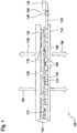
- Fig. 1 shows a power component 100 consisting of a current input plate 105 and a current output plate 110.
- a component carrier 120 in the form of a printed circuit board is arranged between the current input plate 105 and the current output plate 110.
- a plurality of power semiconductors 125 are arranged on the component carrier 120.
- the power semiconductors 125 each have a metal housing 130 which is connected to the current input of the power semiconductors 125.
- the metal housing 130 of the power semiconductor 125 is connected to the current input plate 105 in a directly electrically conductive manner by means of soldering or sintering.
- solder or sinter paste 155 is applied over the surface of the housing 130 of the semiconductor 125.
- the current outputs of the power semiconductors 125 are connected to the current output plate 110 indirectly by means of electrical connection means 160, as vertical vias through the component carrier 120, by means of soldering and / or sintering and / or by means of copper domes (not shown), which are part of the current output plate 110 can, electrically connected.
- a solder resist can be provided on the current output plate 110, except for the contact points with the connecting means.
- a flat housing 130 is preferably used, which protects the power semiconductor 125 at least on one side, has good thermal conductivity and facilitates a large-area connection to the plates 105, 110.
- the opposite current output of the power semiconductor 125 is designed to be freely accessible without a housing. However, it is also conceivable to use power semiconductors 125 without their own housing in such a power component 100. It is important that the power semiconductors 125 have large-area current inputs and outputs in order to reduce the losses caused by the contact resistances between the current input plate 105, the power semiconductor 125 and the current output plate 135. Furthermore, the power semiconductors 125 must be suitable for transmitting high currents in the kA range. Copper plates are provided as the electrically conductive current input / output plate 105, 110. A control connection 135 for the power semiconductors 125 is also shown.
- the current inputs of several MOSFET power semiconductors 125 are connected to the current input plate 105 and the current outputs of these MOSFET power semiconductors 125 are connected to the current output plate 110.
- Both copper plates 105, 110 are arranged parallel and at a small distance from one another.
- All control connections 135 of semiconductors 125 are electrically connected on the printed circuit board of component carrier 120.
- the common control connection 135 is led out to contacts 145 arranged laterally on the printed circuit board of the component carrier 120 and is accessible from the outside via a plug 150.
- the control device 140 is electrically connected to the component carrier 120 by means of the contacts 145 of the plug 150 of the component carrier 120.
- the copper plates 105, 110 which are arranged parallel and flush with one another in their edge area, are connected to one another at least in their edge area by means of an electrically non-conductive plate connecting means 165, so that the copper plates 105, 110 with the connecting means 165 form a housing for the power component 100.
- the high electrical current 180 flowing during the operation of the transformer device 200 can be controlled by means of the control connections 135 of the power semiconductors 125.
- the heat generated in the power semiconductors 125 by the current flow 180 can be dissipated from the power semiconductors 125 in the direction of the current input plate 105 and in the direction of the current output plate 110. This behavior is to be achieved using the in Fig. 1 be indicated arrows 190 shown.
- a temperature sensor 170 is arranged in the immediate vicinity of the power semiconductors 125 on the component carrier 120.
- a thermistor with a negative temperature coefficient based on silicon is particularly advantageously used as the temperature sensor 170.
- thermistors are used in a temperature range from -50 ° C to +150 ° C and are characterized by their small size, tight tolerances and good long-term stability. This enables a very precise temperature measurement.
- the temperature sensor 170 is arranged directly on one of the vias 160 through the component part carrier 120. The temperature sensor 170 is thus placed in the immediate vicinity of the semiconductor 125 and can thereby very precisely detect a temperature of the semiconductor 125 that is very close to the junction temperature.
- four power semiconductors 125 are shown. It is conceivable to arrange further temperature sensors (not shown) on the vias of the current outputs of further power semiconductors 125. This enables spatially resolved detection of the temperature of the power semiconductors 125 of the power component 100.
- the connections of the temperature sensor 170 and any other temperature sensors are routed to the connector 145 on the circuit board of the component carrier 120 and are accessible from the outside via the connector 145. It is particularly advantageous to route the signals from temperature sensor 170 or from all temperature sensors to plug connector 145 via a common bus. A 1-wire bus, an I 2 C bus or a field bus is conceivable here.
- the connection or connections for the temperature sensor 170 is / are led out laterally by means of contacts 145 on the component carrier 120 and thus accessible from the outside via the plug connector 150.
- Fig. 1 The embodiment shown can only be seen roughly schematically and is not intended to suggest any limitation in the number of power semiconductors 125 and temperature sensors 170 used.
- any number of power semiconductors 125 can be connected in parallel in this way and any number of temperature sensors 170 can also be arranged on the power component 100 and detected with the detection device 240.
- a temperature sensor 170 is assigned to each power semiconductor 125.
- the power semiconductors 125 can be arranged in several rows and columns.
- a plurality of temperature sensors 170 can be arranged at predetermined, possibly even distances between the rows or also in the form of a matrix.
- Fig. 2 shows schematically an exemplary embodiment of a transformer device 200 according to the invention.
- the transformer device 200 comprises a transformer 210 with a primary winding 220 and a secondary winding 230.
- the input voltage for the primary winding 220 of the transformer 210 is a pulse-width modulated (PWM) voltage in the range between approx. -500 and +500 volts with a duty cycle between 0 and 100% with a period duration in the range of one millisecond.
- PWM pulse-width modulated
- the output voltage at the secondary winding 230 of the transformer 210 is an open circuit voltage between -10 and + 10V and a current strength of, for example, 7 kA up to 50 kA for typical welding applications.
- two power components 100 are used in the exemplary embodiment as described above, which are only shown schematically in this figure. It is also conceivable to use more than two power components 100 for rectifying the welding current 180.
- the power components 100 each include several, for example four, 9, 16, 25, or 36 power semiconductors 125 and a temperature sensor 170. Other numbers of power semiconductors 125 are of course also conceivable. However, it would also be conceivable to equip only one of the two power components 100 with a temperature sensor 170, for example for an operating case in which the two power components 100 are loaded approximately equally. If there are differences in the cooling due to structural conditions, the power component 100 with the less good cooling connection is expediently equipped with the temperature sensor 170.
- a plurality of temperature sensors 170 to be arranged on each power component 100 in order, as described above, to detect and evaluate a more precise or spatially resolved temperature of the power semiconductors 125.
- temperature sensors 170 it is possible to arrange temperature sensors 170 such that a temperature sensor is assigned to each power semiconductor 125.
- the transformer 210 has a transformation ratio of approx. 50. That is, it transforms the voltage of approx. 500 volts of the primary winding 220 into a voltage in the range of approx. 10V of the secondary winding 230.
- the secondary winding 230 has a center tap 235 with one pole of welding electrodes 290 is connected. If a positive voltage is applied to the primary winding 220, a positive voltage is also applied to the secondary winding 230. In this phase, the upper power component 100 switches through, while the lower power component 100 is blocked and a positive voltage is applied to the welding electrodes 290.
- the welding current 180 flows from the upper tap of the secondary winding 230 of the transformer 210 via the upper power component 100, via the welding electrodes 290 to the center tap 235 of the secondary winding 230 of the transformer 210. If there is a negative voltage on the primary winding 220, then the secondary winding 230 is present also a negative voltage. In this phase, the lower power component 100 switches through, while the upper power component 100 is blocked and to the A positive voltage is again applied to welding electrodes 290. The welding current 180 flows from the lower tap of the secondary winding 230 of the transformer 210 via the lower power component 100, via the welding electrodes 290 to the center tap 235 of the secondary winding 230 of the transformer 210.
- the time profile of the welding current 244, the voltage drop 246 across the power semiconductors 125 and at least the temperatures 242 measured by the temperature sensors 170 of the two power components 100 are recorded by a recording device 240.
- the outputs of the current sensor, the voltage sensor on the power semiconductors 125 and the temperature sensors 170 of the power components 100 are electrically connected to the input of the detection device 240. It is particularly advantageous to route the signals from all sensors to the detection device 240 via a common bus.
- a 1-wire bus, an I 2 C bus or a field bus is conceivable here.
- the detection device 240 detects the time profile of the welding current 180, the voltage drop 246 across the power semiconductors 125 and the temperature profile of the temperature of the power semiconductors 125 of the power components 100 measured by the temperature sensor 170.
- the temperature sensor 170 is placed in the immediate vicinity of the power semiconductor 125 and can therefore be a measure the temperature of the semiconductor 125, which is very close to the junction temperature, very precisely.
- the detection device 240 is part of the welding transformer device 200, as is that of the transformer 210 and the power components 100.
- the transformer device 200 also includes an evaluation device 260.
- the evaluation device 260 is supplied with the measurement data of the sensors recorded by the detection device 240.
- the maintenance time and / or the predicted end of service life of the transformer device 200 is calculated on the basis of the time profile of the individual or combined measured values of the sensors measured with the detection device 240.
- a basis is the determination of the number of junction temperature increases with the boundary conditions offset temperature level and temperature gradient d ⁇ / dt. In this way, knowledge about the operational load of the power semiconductors 125 and aging indicators can be derived.
- the basis for this is the Arrhenius equation, which approximately describes the quantitative change in the parameters in physical and chemical processes.
- the service life function of a power semiconductor depends on the one hand on the height of the junction temperature lift and on the other hand on the mean junction temperature. Reference should be made at this point to the application manual " Power semiconductors "from Semikron, ISBN 978-3-938843-85-7, Verlag ISLE Ilmenau , in particular to chapter 2.7.6 "Evaluation of the temperature curves with regard to the service life".
- the service life or the number of possible load strokes decreases with increasing middle barrier layer.
- the number of possible load changes for temperature swings> 30 K in the barrier layer decreases by a power of ten for every 20 ... 30 K increase in the mean barrier layer temperature. It is therefore extremely important to know the mean junction temperature and also to ensure that the mean junction temperature does not exceed a maximum permissible threshold, since otherwise the temperature fluctuations - due to the power loss during the welding process - have a disproportionate effect on the service life of the power semiconductors.
- Another basis for determining a maintenance time is the calculation of the forward resistance R DSON of the power semiconductors 125 or of the individual power components 100 on the basis of the flowing welding current 180 and the voltage drop 246 across the power semiconductors 125.
- a power component 100 is simplified as a parallel connection of the in it arranged power semiconductor 125 viewed.
- the forward resistance R DSON of the line components 100 is monitored during ongoing operation, on the other hand the determined R DSON values are compared with previous R DSON values - in particular with the value of R DSON when the transformer device 200 or the power components were first started up .
- the values of the welding current and voltage at the welding electrodes 290 are recorded as actual values for the adaptive control mode.
- This welding current 180 which is then detected anyway, can be used to calculate the resistance of the power component 100 R DSON in the evaluation device 260 in the switched-through state.
- the voltage drop 246 across the power semiconductors 125 is also measured as an actual variable for the control device 140 anyway in order to control the control connections 135 for the semiconductors 125 and can therefore be used advantageously to determine R DSON . From the variation over time of this forward resistance R DSON of the power component 100 or the power semiconductor 125, a further parameter for determining the can be determined in the evaluation device 260 as described Determine the maintenance time of the power component 100 and thus of the transformer device 200.
- the current state of wear of the power component 100 can be inferred from the current value of the forward resistance based on the value of the forward resistance at the beginning of the service life of the power component 100 and from its time profile.
- a sudden increase in the value of R DSON particularly indicates an imminent failure of the power component 100.
- the recorded current / voltage and temperature values can also be transmitted to a welding controller 300 or to an external processing unit 400 via a communication device 250.
- This has the advantage that the maintenance time and / or the predicted end of service life of the transformer device 200 can be calculated with the welding control 300 or with the external processing device 400.
- the external processing device 400 is, for example, a server from the manufacturer of the transformer device 200, which is made available as an internet-based cloud connection
- the data from a large number of transformer devices 200 can be collected, edited and processed.
- the algorithms for machine learning can be adapted, improved and optimized independently of the transformer device 200 in the cloud. It is thus possible, for example, to make predictions for the end of the service life of the welding transformer device 200 as a function of production data, power components 100 used, power semiconductors 125 used, etc. It is also conceivable to detect errors in a production batch of the transformer device.
- Other cloud-based applications are conceivable and possible.
- new business models are possible.
- a usage fee for the welding transformer device 200 on the basis of a usage-dependent fee, such as the number of welds performed.
- a load-dependent or wear-dependent usage fee is meant here in particular a calculation of the usage fee that is dependent on the value of the temperature lift.
- the output of evaluation device 260 is a signal that indicates that the number of load changes that are still possible has fallen below a threshold and that a maintenance time for power component 100 and / or transformer device 200 is pending. This signal is fed to a signaling device 270.
- the signaling device 270 is arranged in the transformer device 200 and is used to signal the maintenance time reached directly on the welding transformer device 200.
- the signaling device 270 can be designed as a display, light emitting diode, etc. If the signaling device 270 is designed as a display, for example, the calculated remaining number of load lifts can be displayed on it.
- the remaining number of load lifts is transmitted, for example, from the external processing device 400 via the first communication device 250 to the signaling device 270 and displayed on the display of the signaling device 270. This is indicated by the arrows in Fig. 2 shown.
- the value of R DSON is increasing rapidly. or the temperature of the power component 100 is too high, which can indicate a problem in the cooling system and indicates increased wear.
- the monitoring of the cooling system in particular a basically existing water flow with water cooling, can be implemented simply and advantageously on the basis of the recorded sensor data welding current 244 and temperature 242, in particular the ratio of the rate of increase of the temperature to the duration of the current flow. If the temperature rises too high, based on the duration of the welding current (energy balance), the signaling device 270 can report the lack of cooling.
- the signaling device 270 can also be implemented in the welding control 300 or in the external processing device 400.
- a second wireless communication device 280 additionally or alternatively transmits the maintenance signal via a wireless protocol such as Bluetooth, LoRa and / or ZigBee or via a wired protocol such as Sercos or Ethernet to a production management system of the Operator of the welding system or to a mobile device of an employee of the operator of the transformer device 200 in order to signal a maintenance condition or a maintenance request of the transformer device 200 or a problem with the cooling system of the transformer device 200.
- the operator of the installation or the employee of the operator can activate the corresponding steps for maintenance of the transformer device 200. So it is easy to find a To anticipate failure of the transformer device 200 and the resulting downtimes of the entire system of the operator.
- a power component for controlling a high electrical current comprising a current input plate, a current output plate and a component carrier between these plates with at least two parallel-connected power semiconductor valves arranged on it and with at least one control connection for controlling the power semiconductor valves, in which a temperature sensor is provided between the current input plate and the power output plate and is arranged between the at least two power semiconductor valves.
Abstract
Offenbart wird ein Leistungsbauteil 100 zur Steuerung eines elektrischen Starkstromes 180 umfassend eine Stromeingangsplatte 105, eine Stromausgangsplatte 110 und einen Bauteilträger 120 zwischen diesen Platten 105, 110 mit mindestens zwei auf ihm angeordneten parallelgeschalteten Leistungshalbleiterventilen 125 und mit wenigstens einem Steueranschluss 135 zur Ansteuerung der Leistungshalbleiterventile 125, bei dem ein Temperaturfühler 170 vorgesehen ist, der zwischen der Stromeingangsplatte 105 und der Stromausgangsplatte 110 und zwischen den mindestens zwei Leistungshalbleiterventilen 125 angeordnet ist.Disclosed is a power component 100 for controlling a high electrical current 180 comprising a power input plate 105, a power output plate 110 and a component carrier 120 between these plates 105, 110 with at least two power semiconductor valves 125 arranged in parallel and with at least one control connection 135 for controlling the power semiconductor valves 125, in which a temperature sensor 170 is provided, which is arranged between the current input plate 105 and the current output plate 110 and between the at least two power semiconductor valves 125.
Description
Die Erfindung betrifft ein Leistungsbauteil und eine Transformatoreinrichtung zum Widerstandsschweißen.The invention relates to a power component and a transformer device for resistance welding.
Im Zuge des sogenannten Widerstandsschweißens oder Punktschweißens werden Werkstücke stoffschlüssig miteinander verbunden, wobei Schweißelektroden mit einer Elektrodenkraft gegen die zu verschweißenden Werkstücke gepresst werden. Die Schweißelektroden werden für die Dauer einer Stromzeit von einem Schweißstrom durchflossen. Durch eine Widerstandserwärmung der beiden zu verschweißenden Werkstücke an dem Schweißpunkt zwischen den Schweißelektroden werden die zu verbindenden Werkstücke bis zum Erreichen einer erforderlichen Schweißtemperatur erhitzt und bilden dabei eine Schmelze aus.In the course of so-called resistance welding or spot welding, workpieces are materially connected to one another, with welding electrodes being pressed against the workpieces to be welded with an electrode force. A welding current flows through the welding electrodes for the duration of a current time. Resistance heating of the two workpieces to be welded at the welding point between the welding electrodes causes the workpieces to be connected to be heated until a required welding temperature is reached, thereby forming a melt.
Ein Transformator hat dabei die Aufgabe die Netzspannung oder eine Ansteuerspannung auf eine niedrigere Sekundärspannung herabzusetzen, um den Schweißstrom auf eine Stromstärke von mehreren tausend Ampere zu erhöhen. Der Transformator induziert an seiner Sekundärwicklung eine niedrige Wechselspannung in der Größenordnung von ca. 10 Volt, welche gleichgerichtet wird. Über die Schweißelektroden und die zu verschweißenden Werkstücke fließt ein hoher Gleichstrom in der Größenordnung von 7 bis zu 50 kA, der für den Schweißvorgang verwendet wird. Bedingt durch die niedrige Schweißspannung und die hohen Ströme wird die Verlustleistung des Transformators hauptsächlich durch die Flussspannung der Halbleiterdioden zur Gleichrichtung des Schweißstromes bestimmt. Bei einer Trafoausgangsspannung beim Schweißen von 2,8 V und einer Flussspannung der Gleichrichterdioden von 0,7 Volt ergibt sich allein aufgrund des Spannungsabfalls über die Gleichrichterdioden eine Verlustleistung von 25% bezogen auf die Gesamtleistung des Schweißtransformators. Durch den Einsatz von Halbleiterschaltelementen mit einer geringeren Flussspannung ist es möglich die Verlustleistung zu reduzieren. Es ist bekannt, die Gleichrichterdioden unter anderem durch Schottky-Dioden oder durch Bipolartransistoren mit isolierter Gate Elektrode IGBT, Feldeffekttransistoren FET bzw. Metall-Oxyd Feldeffektransistoren MOSFET mit einer geeigneten Ansteuerung zu ersetzen, um die Verlustleistung zu reduzieren. Um die für den Schweißvorgang erforderlichen hohen Ströme gleichzurichten wird eine entsprechende Anzahl dieser Halbleiterschaltelemente parallelgeschaltet.A transformer has the task of reducing the mains voltage or a control voltage to a lower secondary voltage in order to increase the welding current to an amperage of several thousand amperes. The transformer induces a low alternating voltage in the order of magnitude of approx. 10 volts on its secondary winding, which is rectified. A high direct current of the order of 7 to 50 kA flows through the welding electrodes and the workpieces to be welded and is used for the welding process. Due to the low welding voltage and the high currents, the power loss of the transformer is mainly determined by the forward voltage of the semiconductor diodes for rectifying the welding current. With a transformer output voltage during welding of 2.8 V and a forward voltage of Rectifier diodes of 0.7 volts result in a power loss of 25% based on the total power of the welding transformer due to the voltage drop across the rectifier diodes. By using semiconductor switching elements with a lower forward voltage, it is possible to reduce the power loss. It is known to replace the rectifier diodes by Schottky diodes or by bipolar transistors with an insulated gate electrode IGBT, field effect transistors FET or metal-oxide field effect transistors MOSFET with a suitable control in order to reduce the power loss. In order to rectify the high currents required for the welding process, a corresponding number of these semiconductor switching elements are connected in parallel.
Die Schrift
Als Transformatoren werden für das Widerstandsschweißen seit einiger Zeit Mittelfrequenz-Transformatoren (MF-Transformatoren) eingesetzt. Die Frequenz mit der MF-Transformatoren betrieben werden, ermöglicht eine effektive Energieumwandlung und damit das Verwenden eines relativ kleinen und leichten Transformators. Der Markt tendiert aus Gründen immer höherer Anforderungen an die erforderlichen Bauräume zur Entwicklung immer kleinerer und leistungsfähigerer MF-Transformatoren. Der MF-Transformator kann verkleinert werden, indem man die Schaltfrequenz erhöht. Beim Widerstandsschweißen werden MF-Transformatoren mit einer Schaltfrequenz im Bereich von 1000 Hz eingesetzt. Eine solch hohe Schaltfrequenz vergrößert jedoch die Schaltverluste der eingesetzten Halbleiterschaltelemente.Medium-frequency transformers (MF transformers) have been used as transformers for resistance welding for some time. The frequency with which MF transformers are operated enables an effective energy conversion and thus the use of a relatively small and light transformer. The market is tending towards the development of ever smaller and more powerful MF transformers for reasons of increasing demands on the required installation space. The MF transformer can be made smaller by increasing the switching frequency. MF transformers with a switching frequency in the range of 1000 Hz are used for resistance welding. However, such a high switching frequency increases the switching losses of the semiconductor switching elements used.
Dies wiederum wirkt sich erschwerend auf die Kühlung der verwendeten Leistungshalbleitermodule für die Gleichrichtung des Schweißstromes aus. Für MF-Schweißtransformatoren wird deshalb ein geschlossener Kühlkreislauf empfohlen. Häufig bildet eine elektronische Leistungsstufe mit Leistungshalbleitern zur Gleichrichtung des Schweißstromes zusammen mit dem MF-Transformator eine bauliche Einheit. MF-Schweißtransformatoren sind in der Regel mit einer Wasserkühlung und einer Temperaturüberwachung versehen, denn zu hohe Temperaturen können sowohl das Wicklungspakets des MF-Transformators als auch die, für die Gleichrichtung des Schweißstromes verwendeten Halbleiterbauteile schädigen und zum Ausfall des MF-Schweißtransformators führen. Man kann dann zwar defekte Halbleiterbauteile erkennen, zum Beispiel den Ausfall defekter Leistungsdioden, ein Austausch des Transformators oder der Leistungsbauteile ist dann jedoch erforderlich und erfordert in einer Produktionsanlage nicht akzeptierbare Ausfallzeiten. Um diesen Ausfallzeiten vorzubeugen, wird versucht eine Überlast des Transformators zu erkennen und zu vermeiden. Das erfolgt meist mit einer Temperaturüberwachung. Die Temperaturüberwachung wird üblicherweise mittels Kaltleitern (positiver Temperaturkoeffizient, PTC) realisiert, welche in die Wicklungen der Primär- und Sekundärseite des Transformators eingebracht werden und somit die Wicklungstemperaturen überwachen. Durch Überlast können nämlich Spontanausfälle des Schweißtransformators auftreten. Deshalb ist es sinnvoll einen Überlastbetrieb zu erkennen.This in turn has an aggravating effect on the cooling of the power semiconductor modules used for rectifying the welding current. For MF welding transformers a closed cooling circuit is therefore recommended. Often an electronic power stage with power semiconductors for rectifying the welding current together with the MF transformer forms a structural unit. MF welding transformers are usually provided with water cooling and temperature monitoring, because excessively high temperatures can damage both the winding package of the MF transformer and the semiconductor components used to rectify the welding current and lead to failure of the MF welding transformer. Defective semiconductor components can then be recognized, for example the failure of defective power diodes, but replacement of the transformer or the power components is then necessary and requires unacceptable downtimes in a production plant. In order to prevent these downtimes, an attempt is made to identify and avoid an overload of the transformer. This is usually done with temperature monitoring. Temperature monitoring is usually implemented by means of PTC thermistors (positive temperature coefficient, PTC), which are inserted into the windings of the primary and secondary side of the transformer and thus monitor the winding temperatures. Spontaneous failure of the welding transformer can occur due to overload. Therefore it makes sense to recognize an overload operation.
Aus der Schrift
Die Schrift
Aufgabe der vorliegenden Erfindung ist es deshalb, eine einfache und kostengünstige Überwachungseinrichtung für den Verschleißzustand der Leistungsbauteile eines Schweißtransformators unter Berücksichtigung des Einflusses des Kühlkreislaufes zur Verfügung zu stellen, die die Nachteile der vorgestellten Lösungen umgeht und die keine zusätzliche aufwändige elektronische Schaltung erfordert.The object of the present invention is therefore to provide a simple and inexpensive monitoring device for the state of wear of the power components of a welding transformer, taking into account the influence of the cooling circuit, which circumvents the disadvantages of the solutions presented and which does not require any additional complex electronic circuit.
Leistungshalbleiter haben bekanntermaßen eine begrenzte Lebensdauer. Grundlage der vorliegenden Erfindung ist, dass bei bekannter Höhe des Temperaturhubs sowie bekannter Höhe der mittleren Temperatur - bei welcher besagter Temperaturhub erfolgt - auf die Lebensdauer von Leistungshalbleitern geschlossen werden kann. Grundlage dafür ist die Arrhenius-Gleichung, die die quantitative Temperaturabhängigkeit bei physikalischen und chemischen Prozessen näherungsweise beschreibt. Die Bewertung der Lebensdauer eines Leistungshalbleiters kann mit einer Bewertung der Temperaturverläufe bei den durchgeführten Schaltzyklen (Off/On/Off-Zyklen) erfolgen. Bestimmt wird der Verschleiß der Halbleiter somit durch die Anzahl der Sperrschichttemperaturhübe bei vorgegebener Offsettemperatur. Ganz grob bedeutet beispielsweise bei den heutigen Schweißdioden ein Hub von 60 °K etwa eine Lebensdauer von 10 Millionen Schweißungen bei einer mittleren Temperatur von 70 °C. Mit größerer Offsettemperatur erhöht sich der Verschleiß und die Lebensdauer des Leistungshalbleiters verringert sich. Die Halbleiterhersteller geben in ihren Datenblättern Auskunft darüber, inwieweit sich die Lebensdauer in Abhängigkeit von der Höhe der Temperaturhübe und der Höhe der Offsettemperatur verringert. Grundlage für die Berechnung der Restlebensdauer des Leistungshalbleiters ist somit die Erfassung der Temperatur in der Sperrschicht des Leistungshalbleiters. So ist die Lebensdauerfunktion eines Leistungshalbleiters zum einen abhängig von der Höhe des Temperaturhubes der Sperrschichttemperatur, zum anderen von der mittleren Sperrschichttemperatur. Herkömmliche Schweißdioden bestehen aus einer Siliziumscheibe zwischen zwei Metallscheiben. Solche Bauelemente sind druckkontaktiert, so dass es hier keine Möglichkeit gibt sperrschichtnah einen Temperaturfühler zu platzieren.It is known that power semiconductors have a limited service life. The basis of the present invention is that with a known level of the temperature rise and a known level of the mean temperature - at which said temperature rise takes place - conclusions can be drawn about the service life of power semiconductors. The basis for this is the Arrhenius equation, which approximately describes the quantitative temperature dependence in physical and chemical processes. The service life of a power semiconductor can be assessed by assessing the temperature curves during the switching cycles carried out (off / on / off cycles). The wear of the semiconductors is thus determined by the number of junction temperature increases at a given offset temperature. In today's welding diodes, for example, a stroke of 60 ° K roughly means a service life of 10 million welds at an average temperature of 70 ° C. With A higher offset temperature increases the wear and tear and the service life of the power semiconductor is reduced. The semiconductor manufacturers provide information in their data sheets about the extent to which the service life is reduced depending on the level of the temperature swings and the level of the offset temperature. The basis for calculating the remaining service life of the power semiconductor is therefore the detection of the temperature in the junction of the power semiconductor. The service life function of a power semiconductor depends on the one hand on the level of the temperature swing of the junction temperature and on the other hand on the mean junction temperature. Conventional welding diodes consist of a silicon disk between two metal disks. Such components are pressure-contacted so that there is no possibility of placing a temperature sensor near the barrier layer.
Vor diesem Hintergrund werden ein Leistungsbauteil und eine Transformatoreinrichtung zum Widerstandsschweißen mit den Merkmalen der unabhängigen Patentansprüche vorgeschlagen.Against this background, a power component and a transformer device for resistance welding with the features of the independent patent claims are proposed.
Für das bevorzugte Leistungsbauteil mit Stromeingangsplatte, Stromausgangsplatte und mit einem Bauteilträger wird zwischen diesen Platten ein Temperaturfühler vorgesehen, der zwischen der Stromeingangsplatte und der Stromausgangsplatte und zwischen den mindestens zwei Leistungshalbleiterventilen angeordnet ist. Durch diese Anordnung des Temperaturfühlers, kann die mittlere Temperatur der Leistungshalbleiterventile und deren Gradient über der Zeit sehr einfach, genau und nah an der Sperrschicht der Leistungshalbleiterventile - zumindest nah am Halbleitermaterial - erfasst werden. Die so gemessene Temperatur kann sogar näherungsweise mit der oben genannten Sperrschichttemperatur gleichgesetzt werden, weil bei einem Leistungsbauteil in dieser Bauweise Temperarturabfälle im Material wegen der schnellen Wärmeabfuhr kaum auftreten. Diese somit sperrschichtnahe Temperaturmessung ermöglicht während der Schaltzyklen der Leistungshalbleiter die Erfassung sowohl des Offsetniveaus der Temperatur, wodurch der Einfluss der Wasserkühlung berücksichtigt ist, als auch die Ermittlung der Änderungen der Sperrschichttemperatur der verwendeten Halbleiterventile über der Zeit und damit der Höhe des Temperaturhubes. Durch geeignete Auswertung zum Beispiel in einer Auswerteeinrichtung des Schweißtransformators, in einer Auswerteeinrichtung der Schweißsteuerung bzw. in einer externen Verarbeitungseinheit ist somit die Ermittlung des Lebensdauerendes sowie die Signalisierung des Zeitpunktes eines Austausches des Transformators möglich, ohne dass weitere elektronische Schaltungen die Lebensdauer des Transformators einschränken. Dafür kann z.B. eine Aggregation von Temperaturhüben erfolgen, z.B. segmentiert nach Höhe des einzelnen Temperaturhubs und Offsettemperatur.For the preferred power component with current input plate, current output plate and with a component carrier, a temperature sensor is provided between these plates, which is arranged between the current input plate and the current output plate and between the at least two power semiconductor valves. With this arrangement of the temperature sensor, the mean temperature of the power semiconductor valves and their gradient over time can be recorded very simply, precisely and close to the barrier layer of the power semiconductor valves - at least close to the semiconductor material. The temperature measured in this way can even be approximately equated with the above-mentioned junction temperature, because with a power component of this type there is hardly any temperature drop in the material due to the rapid dissipation of heat. This temperature measurement, which is close to the junction layer, enables both the temperature offset level to be recorded during the switching cycles of the power semiconductors, which takes into account the influence of the water cooling, as well as the determination of the changes in the junction temperature of the semiconductor valves used over time and thus the level of the temperature swing. By suitable evaluation, for example in an evaluation device of the welding transformer, in an evaluation device of the welding controller or in an external processing unit, it is possible to determine the end of the service life and to signal the time of replacement of the transformer without further electronic circuits affecting the service life of the Restrict transformer. For this purpose, for example, an aggregation of temperature swings can take place, for example segmented according to the level of the individual temperature swings and offset temperature.
Versagt die Kühlung des Schweißtransformators, so wird das in kurzer Zeit zum Ausfall des Schweißtransformators führen. Deshalb sind nach dem Stand der Technik Maßnahmen vorgesehen, einen Ausfall des Kühlsystems zu erkennen. Dies geschieht in der Regel durch Sensorik für Durchflussmessung, Druckmessung oder Temperaturmessung im Kühlkreislauf. Ein Ausfall des Kühlsystems bewirkt eine Erhöhung des Temperaturniveaus im Leistungsbauteil, was zuverlässig durch Auswertung des Offsetniveaus des Temperaturfühlersignals erkannt wird. Dadurch kann die im Stand der Technik notwendige Sensorik zur Erkennung eines Ausfalls des Kühlsystems entfallen und somit allein durch Auswertung des Temperaturfühlersignals erfolgen. Mit dem ohnehin erfindungsgemäß vorhandenem Temperaturfühler kann somit auch der Ausfall des Kühlsystems erkannt werden, und zwar rechtzeitig bevor eine Zerstörung des Leistungsbauteils erfolgt. Damit lassen sich in besonders vorteilhafter und einfacher Art und Weise zum einen die Ausfallzeiten durch vorbeugenden Austausch der Leistungsbauteile des Schweißtransformators vor Ende der Lebensdauer verhindern, zum anderen lässt sich einer Zerstörung des Leistungsbauteils bei Ausfall des Kühlsystems zuvorkommen.If the cooling of the welding transformer fails, this will quickly lead to failure of the welding transformer. Therefore, according to the state of the art, measures are provided to detect a failure of the cooling system. This is usually done by sensors for flow measurement, pressure measurement or temperature measurement in the cooling circuit. A failure of the cooling system causes an increase in the temperature level in the power component, which is reliably detected by evaluating the offset level of the temperature sensor signal. As a result, the sensors required in the prior art to detect a failure of the cooling system can be dispensed with and can therefore only be carried out by evaluating the temperature sensor signal. With the temperature sensor, which is present according to the invention, the failure of the cooling system can thus also be detected, specifically in good time before the power component is destroyed. In this way, on the one hand, downtimes can be prevented in a particularly advantageous and simple manner by preventive replacement of the power components of the welding transformer before the end of the service life, and on the other hand, destruction of the power component in the event of failure of the cooling system can be prevented.
Vorteilhafte Weiterbildungen sind Gegenstand der Unteransprüche sowie der nachfolgenden Beschreibung.Advantageous further developments are the subject of the subclaims and the following description.
Als Temperaturfühler wird besonders vorteilhaft ein Heißleiter mit einem negativen Temperaturkoeffizienten auf Siliziumbasis eingesetzt. Diese Heißleiter werden in einem Temperaturbereich von -50 °C bis +150 °C eingesetzt und zeichnen sich durch geringe Baugröße, enge Toleranzen und gute Langzeitstabilität aus. Damit ist eine sehr genaue Temperaturmessung möglich.A thermistor with a negative temperature coefficient based on silicon is particularly advantageously used as the temperature sensor. These thermistors are used in a temperature range from -50 ° C to +150 ° C and are characterized by their small size, tight tolerances and good long-term stability. This enables a very precise temperature measurement.
Besonders vorteilhaft ist es zudem, den Temperaturfühler auf dem Bauteilträger des Leistungsbauteils anzuordnen. Dadurch ist der Temperaturfühler in unmittelbarer Nähe der Halbleiterschaltelemente platziert und kann dadurch eine der Sperrschichttemperatur nahekommende Temperatur der verwendeten Halbleiter sehr genau erfassen.It is also particularly advantageous to arrange the temperature sensor on the component carrier of the power component. As a result, the temperature sensor is placed in the immediate vicinity of the semiconductor switching elements and can therefore very precisely detect a temperature of the semiconductor used that is close to the junction temperature.
Weiterhin von Vorteil ist es, den Anschluss des Temperaturfühlers und/oder den wenigstens einen Steueranschluss zur Ansteuerung der Leistungshalbleiterventile des Leistungsbauteils zu Kontakten eines Steckers des Bauteilträgers des Leistungsbauteils nach außen zu führen. Wenn der Stecker des Bauteilträgers des Leistungsbauteils seitlich über die Stromeingangsplatte die Stromausgangsplatte heraussteht, ist es besonders einfach das Leistungsbauteil mit den Anschlüssen für die Steuerung und den Temperaturfühler zu kontaktieren. Solch ein Leistungsbauteil ist für die Gleichrichtung des Ausgangsstromes der Sekundärwicklung eines erfindungsgemäßen Schweißtransformators besonders gut geeignet, da es sowohl für die hohen Schweißströme und die niedrigen Spannungen - welche auf der Sekundärseite des Transformators auftreten - ausgelegt ist und einen Stecker auf dem Bauteilträger sowohl für die Kontakte der Ansteuerung, als auch für den Temperaturfühler aufweist. Eine bauliche wassergekühlte Einheit aus Transformator und Leistungsbauteil lässt sich einfach und kostengünstig realisieren. Eine Ansteuereinrichtung, die dazu eingerichtet ist, den Steueranschluss des Leistungsbauteils zur Gleichrichtung des elektrischen Starkstromes zu steuern, kann einfach durch direkte oder indirekte Steckverbindung mit den Kontakten des Steckers des Bauteilträgers kontaktiert werden. Eine Erfassungseinrichtung die, dazu eingerichtet ist das Signal des Temperaturfühlers zu erfassen, kann ebenfalls einfach durch direkte oder indirekte Steckverbindung mit dem Stecker des Bauteilträgers kontaktiert werden. Der Stecker kann auch als überstehender Abschnitt einer den Bauteilträger bildenden Platine ausgebildet sein. Die Erfassung der sperrschichtnahen Temperaturmessung mit besagter Erfassungseinrichtung ermöglicht die Ermittlung der Schaltzyklen, die Auswertung des Offsetniveaus der Temperatur, wodurch der Einfluss der Wasserkühlung berücksichtigt ist, als auch die Ermittlung der Änderungen der Sperrschichttemperatur der verwendeten Halbleiterventile über der Zeit.It is also advantageous to lead the connection of the temperature sensor and / or the at least one control connection for controlling the power semiconductor valves of the power component to contacts of a plug of the component carrier of the power component to the outside. If the plug of the component carrier of the power component protrudes laterally over the power input plate, the power output plate, it is particularly easy to contact the power component with the connections for the control and the temperature sensor. Such a power component is particularly well suited for rectifying the output current of the secondary winding of a welding transformer according to the invention, as it is designed for both the high welding currents and the low voltages - which occur on the secondary side of the transformer - and a connector on the component carrier for the contacts the control, as well as for the temperature sensor. A structural water-cooled unit consisting of a transformer and a power component can be implemented easily and inexpensively. A control device which is set up to control the control connection of the power component for rectifying the high electrical current can be contacted simply by direct or indirect plug connection with the contacts of the connector of the component carrier. A detection device which is set up to detect the signal of the temperature sensor can also be contacted simply by direct or indirect plug connection with the plug of the component carrier. The plug can also be designed as a protruding section of a circuit board forming the component carrier. The detection of the temperature measurement close to the barrier layer with said detection device enables the determination of the switching cycles, the evaluation of the offset level of the temperature, whereby the influence of the water cooling is taken into account, as well as the determination of the changes in the barrier layer temperature of the semiconductor valves used over time.
Wenn weiterhin eine mindestens erste Kommunikationseinrichtung vorhanden ist und dazu eingerichtet ist, den gemessenen zeitlichen Verlauf der sperrschichtnahen Temperatur der mindestens zwei Leistungshalbleiterventile des Leistungsbauteils an eine Schweißsteuerung und/oder an eine externe Verarbeitungseinrichtung zu übertragen, kann die Berechnung der verbleibendenden Lebensdauer in der Schweißsteuerung und/oder in der externen Verarbeitungseinheit erfolgen.If there is also at least a first communication device and is set up to transmit the measured time profile of the temperature near the barrier layer of the at least two power semiconductor valves of the power component to a welding controller and / or to an external processing device, the calculation of the remaining service life in the welding controller and / or or in the external processing unit.
Dies hat den Vorteil, dass keine zusätzliche elektronische Schaltung für die Ermittlung der verbleibenden Lebensdauer des Leistungsbauteils und damit des Schweißtransformators im Schweißtransformator selbst erforderlich ist, die selbst einen, wie bereits oben beschriebenen, Einfluss auf den Verschleiß des Schweißtransformators hätte.This has the advantage that no additional electronic circuit is required for determining the remaining service life of the power component and thus of the welding transformer in the welding transformer itself, which would itself have an influence on the wear of the welding transformer, as already described above.
Denkbar ist es auch, dass die Berechnung der verbleibenden Restlebensdauer in einer Auswerteeinrichtung, die in der Schweißtransformatoreinrichtung angesiedelt ist, erfolgt. Berechnungsgrundlage bildet - wie zuvor bereits angedeutet - eine mit der Offsettemperatur bewertete Aggregation der Temperaturhübe wie nachfolgend anhand eines Ausführungsbeispiels noch näher beschrieben wird. Wird ein vorgegebener Schwellwert der bewerteten Temperaturhübe überschritten, so ist der Wartungszeitpunkt gegeben.It is also conceivable for the remaining service life to be calculated in an evaluation device located in the welding transformer device. The calculation basis - as already indicated - is based on the offset temperature evaluated aggregation of the temperature swings as will be described in more detail below using an exemplary embodiment. If a specified threshold value of the evaluated temperature increases is exceeded, the maintenance time is given.
Wenn die Auswerteeinrichtung zur Kalkulation des Wartungszeitpunktes und/oder des prognostizierten Lebensdauerendes in der Schweißsteuerung und/oder in der externen Verarbeitungseinrichtung angesiedelt ist, kann die Berechnung der verbleibendenden Lebensdauer in der Schweißsteuerung und/oder in der externen Verarbeitungseinheit erfolgen.If the evaluation device for calculating the maintenance time and / or the forecast end of service life is located in the welding control and / or in the external processing device, the remaining service life can be calculated in the welding control and / or in the external processing unit.
Von besonderen Vorteil ist es, den in der Schweißsteuerung oder der externen Verarbeitungseinrichtung berechneten Wartungszeitpunkt über die Kommunikationseinrichtung zurück an den Schweißtransformator zu übertragen.It is particularly advantageous to transmit the maintenance time calculated in the welding control or the external processing device back to the welding transformer via the communication device.
Mit einer Signalisierungseinrichtung der Transformatoreinrichtung kann der erreichte Wartungszeitpunkt und/oder das prognostizierte Lebensdauerende der Transformatoreinrichtung direkt an der Transformatoreinrichtung angezeigt werden.With a signaling device of the transformer device, the maintenance time reached and / or the predicted end of service life of the transformer device can be displayed directly on the transformer device.
Wenn der Wartungszeitpunkt erreicht ist, kann die Notwendigkeit eines Austausches des Transformators oder des erfindungsgemäßen Leistungsbauteiles auch über eine weitere Kommunikationseinrichtung an eine übergeordnete Produktionsleiteinrichtung oder eine App an ein mobiles Usergerät, wie ein Smartphone oder ein Tablet gemeldet werden.When the maintenance time is reached, the need to replace the transformer or the power component according to the invention can also be reported via another communication device to a higher-level production control device or an app to a mobile user device such as a smartphone or tablet.
Von besonderem Vorteil sind hier insbesondere Kommunikationseinrichtungen die über ein Protokoll wie Bluetooth, LoRa und/oder ZigBee drahtlos kommunizieren. Während Lora ist ein Kommunikationsstandard für Funkverbindungen großer Reichweite ist, spezifiziert ZigBee ist drahtlose Netzwerke kurzer Reichweite. Denkbar ist jedoch auch eine kabelgebundene Kommunikation über Ethernet oder Sercos. Sercos ist eine normierte digitale Schnittstelle zur Kommunikation zwischen Steuerungen und Feldbusteilnehmern.Communication devices that communicate wirelessly via a protocol such as Bluetooth, LoRa and / or ZigBee are particularly advantageous here. While Lora is a communication standard for long-range radio links, ZigBee specifies short-range wireless networks. However, wired communication via Ethernet or Sercos is also conceivable. Sercos is a standardized digital interface for communication between controllers and fieldbus participants.
Über einen zweiten Kanal kann die Erfassungseinrichtung weiterhin dazu eingerichtet sein, den zeitlichen Spannungsverlauf an den Schweißelektroden und/oder den zeitlichen Stromverlauf der Sekundärwicklung und/oder der Primärwicklung des Transformators zu erfassen. Damit können insbesondere Überlastsituationen des Leistungsbauteils erkannt und verhindert werden. In einem solchen Fall kann beispielsweise der Schweißstrom abgeschaltet werden, um Folgeschäden durch Überlast zu vermeiden. Dies ermöglicht insbesondere das Verhindern von vorzeitigen Ausfällen des Leistungsbauteils und damit der Schweißtransformatoreinrichtung zum Beispiel durch Überspannungen und zu hohe Ströme.Via a second channel, the detection device can also be set up to detect the temporal voltage profile at the welding electrodes and / or the temporal current profile of the secondary winding and / or the primary winding of the transformer. In this way, in particular, overload situations of the power component can be recognized and prevented. In such a case, for example, the welding current can be switched off in order to avoid consequential damage caused by overload. This makes it possible in particular to prevent premature failure of the power component and thus of the welding transformer device, for example due to overvoltages and excessively high currents.
Das kann insbesondere bei Schweißen von falschen Materialen mit zu geringem Widerstand auftreten oder bei Kurzschlüssen an den Schweißelektroden auftreten.This can occur especially when welding the wrong materials with insufficient resistance or when there are short circuits on the welding electrodes.
Besonders vorteilhaft ist es, diese für eine adaptive Schweißregelung ASR ohnehin erfassten Spannungen und/oder Ströme sowie die für die Ansteuereinrichtung ohnehin erfassten Spannungsabfälle über die Leistungshalbleiter über die erste Kommunikationseinrichtung an die Schweißsteuerung und/oder an die externe Verarbeitungseinrichtung zu übertragen. Dadurch wird es möglich, aus dem erfassten Spannungs- und/oder Stromverlauf in der Auswerteeinrichtung den Istzustand des Verschleißes der Halbleiterventile zu berechnen. Dies erfolgt durch Berechnung des Durchlasswiderstandes des durchgeschalteten Leistungshalbleiters. Aus dem Wert des Durchlasswiderstandes bezogen auf einen Anfangswert des Durchlasswiderstandes des Leistungshalbleiters kann nämlich auf seinen aktuellen Verschleißzustand geschlossen werden. Aus dem Stand der Technik ist bekannt, dass sich der Durchlasswiderstand des Leistungshalbleiters im Laufe der Zeit erhöht. Bei Feldeffekttransistoren wird dieser Durchlasswiderstand als RDSON bezeichnet. Der Name setzt sich aus dem Kürzel für den Drain/Source Widerstand RDS und dem englischen Wort "On", das den durchgeschalteten Zustand des Feldeffekttransistors kennzeichnet, zusammen. Aus dem aktuellen Wert des Durchlasswiderstandes bezogen auf den Wert des Durchlasswiderstandes zu Beginn der Lebensdauer des Leistungshalbleiters sowie aus dessen zeitlichen Verlauf kann auf den aktuellen Verschleißzustand der Leistungshalbleiter geschlossen werden. So deutet eine plötzliche Erhöhung des Wertes von RDSON auf einen kurz bevorstehenden Ausfall des Leistungshalbleiters hin. Da für die Regelung des Schweißstromes sowie für die Ermittlung des Widerstandes an der Schweißstelle, Strom- und Spannung an der Schweißstelle ohnehin gemessen werden, kann ohne Einsatz zusätzlicher Sensorik der aktuelle Wert des Durchlasswiderstandes des Leistungshalbleiters sowie dessen Änderung für die Berechnung des Lebensdauerendes des Leistungsbauteils verwendet werden.It is particularly advantageous to transmit these voltages and / or currents already recorded for an adaptive welding control ASR and the voltage drops already recorded for the control device over the power semiconductors via the first communication device to the welding control and / or to the external processing device. This makes it possible to calculate the actual state of wear of the semiconductor valves from the recorded voltage and / or current profile in the evaluation device. This is done by calculating the forward resistance of the connected power semiconductor. From the value of the forward resistance based on an initial value of the forward resistance of the power semiconductor, conclusions can be drawn about its current state of wear. It is known from the prior art that the forward resistance of the power semiconductor increases over time. In the case of field effect transistors, this forward resistance is referred to as R DSON . The name is made up of the abbreviation for the drain / source resistor R DS and the English word "On", which indicates the switched state of the field effect transistor. The current state of wear of the power semiconductors can be inferred from the current value of the forward resistance in relation to the value of the forward resistance at the beginning of the service life of the power semiconductor, as well as from its time profile. A sudden increase in the value of R DSON thus indicates an imminent failure of the power semiconductor. Since current and voltage at the welding point are measured anyway to control the welding current and to determine the resistance at the welding point, the current value of the forward resistance of the power semiconductor and its change can be used to calculate the end of the service life of the power component without using additional sensors will.
Die Auswerteinheit kann wie bereits oben beschrieben in der Schweißsteuerung als auch in einer externen Verarbeitungseinrichtung angesiedelt sein.As already described above, the evaluation unit can be located in the welding control as well as in an external processing device.
Denkbar ist es auch, dass die Kalkulation des erreichten Wartungszeitpunkts und/oder das prognostizierte Lebensdauerende der Transformatoreinrichtung unter Berücksichtigung des kalkulierten Verschleißes aufgrund der Berechnung des Kennwertes RDSON und dessen zeitlichen Verlauf über der Zeit erfolgt.It is also conceivable that the calculation of the reached maintenance time and / or the predicted end of service life of the transformer device is carried out taking into account the calculated wear on the basis of the calculation of the characteristic value R DSON and its course over time.
Die Verfahren können vorteilhaft kombiniert werden. Während die Aggregation von Temperaturhüben eine Prognose eines Wartungs- oder Ausfallzeitpunktes erlaubt, erlaubt die Messung des Durchlasswiderstandes RDSON eine aktuelle Einschätzung des Verschleißzustandes. Die Prognose könnte z.B. dann mit der aktuellen Einschätzung angepasst und verfeinert werden, z.B. könnte ein Wartungszeitraum nach hinten verschoben werden, wenn der Durchlasswiderstandes RDSON einen geringeren Verschleiß des Leistungshalbleiters anzeigt, als es sich aus der Aggregation der Temperaturhübe errechnet.The methods can advantageously be combined. While the aggregation of temperature fluctuations allows a prognosis of a maintenance or failure time, the Measurement of the forward resistance R DSON an up-to-date assessment of the state of wear. The prognosis could, for example, be adjusted and refined with the current assessment, for example a maintenance period could be postponed if the on- state resistance R DSON indicates less wear of the power semiconductor than is calculated from the aggregation of the temperature increases.
Weitere Vorteile ergeben sich aus der nachfolgenden Beschreibung.Further advantages emerge from the following description.
Die Erfindung wird nun anhand eines Ausführungsbeispiels mit Hilfe der beigefügten Figuren näher beschrieben:
Darin zeigen:
- Fig. 1
- eine Anordnung zur Realisierung eines Leistungsbauteils zur Steuerung eines elektrischen Stromes, und
- Fig. 2
- schematisch eine bevorzugte Ausgestaltung einer erfindungsgemäßen Transformatoreinrichtung.
Show in it:
- Fig. 1
- an arrangement for realizing a power component for controlling an electric current, and
- Fig. 2
- schematically a preferred embodiment of a transformer device according to the invention.
Identische Bezugszeichen in den
Vorzugsweise kommt ein flaches Gehäuse 130 zum Einsatz, welches den Leistungshalbleiter 125 zumindest einseitig schützt, eine gute Wärmeleitfähigkeit aufweist und eine großflächige Anbindung an die Platten 105, 110 erleichtert. Der gegenüberliegende Stromausgang des Leistungshalbleiters 125 ist ohne Gehäuse frei zugänglich ausgeführt. Denkbar ist jedoch auch, in einem solchen Leistungsbauteil 100 Leistungshalbleiter 125 ohne eigenes Gehäuse zu verwenden. Wichtig ist, dass die Leistungshalbleiter 125 großflächige Stromeingänge und Stromausgänge aufweisen, um die Verluste, bedingt durch die Übergangswiderstände zwischen Stromeingangsplatte 105, Leistungshalbleiter 125 und Stromausgangsplatte 135 zu reduzieren. Weiterhin müssen die Leistungshalbleiter 125 zur Übertragung hoher Ströme im kA-Bereich geeignet sein. Als elektrisch leitfähige Stromeingangs-/Stromausgangsplatte 105, 110 sind Kupferplatten vorgesehen. Ein Steueranschluss 135 für die Leistungshalbleiter 125 ist ebenfalls dargestellt.A
Im hier gezeigten Ausführungsbeispiel sind die Stromeingänge mehrerer MOSFET-Leistungshalbleiter 125 mit der Stromeingangsplatte 105 und die Stromausgänge dieser MOSFET-Leistungshalbleiter 125 mit der Stromausgangsplatte 110 verbunden. Beide Kupferplatten 105, 110 sind parallel und in einem geringen Abstand zueinander angeordnet. Alle Steueranschlüsse 135 der Halbleiter 125 sind auf der Leiterplatte des Bauteilträgers 120 elektrisch verbunden. Der gemeinsame Steueranschluss 135 ist zu seitlich auf der Leiterplatte des Bauteilträgers 120 angeordneten Kontakten 145 herausgeführt und von außen über einen Stecker 150 zugänglich. Die Ansteuereinrichtung 140 wird mit dem Bauteilträger 120 mittels der Kontakte 145 des Steckers 150 des Bauteilträgers 120 elektrisch verbunden. Die parallel und in ihrem Randbereich bündig zueinander angeordneten Kupferplatten 105, 110 sind mindestens in ihrem Randbereich mittels eines elektrisch nicht leitfähigen Platten-Verbindungsmittels 165 miteinander verbunden, so dass die Kupferplatten 105, 110 mit dem Verbindungsmittel 165 ein Gehäuse für das Leistungsbauteil 100 bilden.In the exemplary embodiment shown here, the current inputs of several
Der während des Betriebs der Transformatoreinrichtung 200 fließende elektrische Starkstrom 180 kann mittels der Steueranschlüsse 135 der Leistungshalbleiter 125 gesteuert werden. Die durch den Stromfluss 180 erzeugte Wärme in den Leistungshalbleitern 125 kann in Richtung der Stromeingangsplatte 105 und in Richtung der Stromausgangsplatte 110 von den Leistungshalbleitern 125 abgeführt werden. Dieses Verhalten soll mittels der in
Die in
Für die Gleichrichtung des elektrischen Starkstromes 180 der Sekundärwicklung 230 werden im Ausführungsbeispiel zwei Leistungsbauteile 100 wie oben beschrieben verwendet, die in dieser Figur lediglich schematisch dargestellt sind. Denkbar ist es auch, mehr als zwei Leistungsbauteile 100 für die Gleichrichtung des Schweißstromes 180 einzusetzen. Die Leistungsbauteile 100 umfassen jeweils mehrere, z.B. vier, 9, 16, 25, oder 36 Leistungshalbleiter 125 sowie einen Temperaturfühler 170. Auch andere Zahlen der Leistungshalbleiter 125 sind natürlich denkbar. Es wäre jedoch auch denkbar nur eines der beiden Leistungsbauteile 100 mit einem Temperaturfühler 170 auszustatten, z.B. für einen Betriebsfall in dem die beiden Leistungsbauteile 100 etwa gleich stark belastet sind. Wenn es aufgrund baulicher Gegebenheiten Unterschiede in der Kühlung gibt, wird in zweckmäßiger Weise das Leistungsbauteil 100 mit der weniger guten Kühlanbindung mit dem Temperaturfühler 170 ausgestattet. Denkbar ist es auch, wie zuvor in
Der Transformator 210 hat ein Übersetzungsverhältnis von ca. 50. Das heißt, er transformiert die Spannung von ca. 500 Volt der Primärwicklung 220 in eine Spannung im Bereich von ca. 10V der Sekundärwicklung 230. Die Sekundärwicklung 230 hat eine Mittelanzapfung 235 die mit einem Pol der Schweißelektroden 290 verbunden ist. Liegt an der Primärwicklung 220 eine positive Spannung an, so liegt an der Sekundärwicklung 230 ebenfalls eine positive Spannung an. In dieser Phase schaltet das obere Leistungsbauteil 100 durch, während das untere Leistungsbauteil 100 gesperrt ist und an den Schweißelektroden 290 liegt eine positive Spannung an. Der Schweißstrom 180 fließt von der oberen Anzapfung der Sekundärwicklung 230 des Transformators 210 über das obere Leistungsbauteil 100, über die Schweißelektroden 290 zur Mittelanzapfung 235 der Sekundärwicklung 230 des Transformators 210. Liegt an der Primärwicklung 220 eine negative Spannung an, so liegt an der Sekundärwicklung 230 ebenfalls eine negative Spannung an. In dieser Phase schaltet das untere Leistungsbauteil 100 durch, während das obere Leistungsbauteil 100 gesperrt ist und an den Schweißelektroden 290 liegt wiederum eine positive Spannung an. Der Schweißstrom 180 fließt von der unteren Anzapfung der Sekundärwicklung 230 des Transformators 210 über das untere Leistungsbauteil 100, über die Schweißelektroden 290 zur Mittelanzapfung 235 der Sekundärwicklung 230 des Transformators 210.The
Der zeitliche Verlauf des Schweißstromes 244, des Spannungsabfalls 246 über die Leistungshalbleiter 125 sowie zumindest der von den Temperaturfühlern 170 der beiden Leistungsbauteile 100 gemessenen Temperaturen 242 wird durch eine Erfassungseinrichtung 240 erfasst. Die Ausgänge des Stromsensors, des Spannungssensors an den Leistungshalbleitern 125 sowie der Temperaturfühler 170 der Leistungsbauteile 100 sind dazu mit dem Eingang der Erfassungseinrichtung 240 elektrisch verbunden. Besonders vorteilhaft ist es, die Signale aller Sensoren über einen gemeinsamen Bus zur Erfassungseinrichtung 240 zu führen. Denkbar ist hier ein 1-Draht-Bus (1- Wire), ein I2C Bus oder auch ein Feldbus.The time profile of the welding current 244, the
Die Erfassungseinrichtung 240 erfasst den zeitlichen Verlauf des Schweißstromes 180, des Spannungsabfalls 246 über die Leistungshalbleiter 125 sowie den Temperaturverlauf der vom Temperaturfühler 170 gemessenen Temperatur der Leistungshalbleiter 125 der Leistungsbauteile 100. Der Temperaturfühler 170 ist dafür in unmittelbarer Nähe des Leistungshalbleiters 125 platziert und kann deshalb eine der Sperrschichttemperatur sehr nahekommende Temperatur des Halbleiters 125 sehr genau messen. Die Erfassungseinrichtung 240 ist Bestandteil der Schweißtransformatoreinrichtung 200, ebenso wie die der Transformator 210 und die Leistungsbauteile 100.The
Weiterhin umfasst die Transformatoreinrichtung 200 eine Auswerteeinrichtung 260. Der Auswerteeinrichtung 260 werden die mit der Erfassungseinrichtung 240 erfassten Messdaten der Sensoren zugeführt. In der Auswerteinrichtung 260 erfolgt die Berechnung des Wartungszeitpunktes und/oder des prognostizierten Lebensdauerendes der Transformatoreinrichtung 200 auf Basis des mit der Erfassungseinrichtung 240 gemessenen zeitlichen Verlaufs der genannten einzelnen oder kombinierten Messwerte der Sensoren.The
Eine Grundlage ist die Bestimmung der Anzahl der Sperrschichttemperaturhübe mit den Randbedingungen Offsettemperaturniveau und Temperaturgradient dϑ/dt. Auf diese Weise lassen sich Erkenntnisse über die Betriebsbelastung der Leistungshalbleiter 125 sowie Alterungsindikatoren ableiten. Basis dafür ist die Arrhenius-Gleichung, die die quantitative Veränderung der Kenngrößen bei physikalischen und chemischen Prozessen näherungsweise beschreibt. So ist die Lebensdauerfunktion eines Leistungshalbleiters zum einen abhängig von der Höhe des Hubes der Sperrschichttemperatur, zum anderen von der mittleren Sperrschichttemperatur. Verwiesen werden soll an dieser Stelle auf das Applikationshandbuch "
Eine weitere Grundlage für die Ermittlung eines Wartungszeitpunktes stellt die Berechnung des Durchlasswiderstandes RDSON der Leistungshalbleiter 125 oder der einzelnen Leistungsbauteile 100 auf Basis des fließenden Schweißstromes 180 sowie des Spannungsabfalls 246 über die Leistungshalbleiter 125 dar. Dabei wird vereinfacht ein Leistungsbauteil 100 als Parallelschaltung der in ihm angeordneten Leistungshalbleiter 125 angesehen. Dafür wird zum einen der Durchlasswiderstand RDSON der Leitungsbauteile 100 während des laufenden Betriebes überwacht, zum anderen werden die ermittelten RDSON Werte mit zeitlich zurückliegenden RDSON Werten - insbesondere mit dem Wert von RDSON bei Erstinbetriebnahme der Transformatoreinrichtung 200 bzw. der Leistungsbauteile - verglichen.Another basis for determining a maintenance time is the calculation of the forward resistance R DSON of the
Übersteigt der Wert von RDSON einen Schwellwert bzw. überschreitet die Anstiegsgeschwindigkeit von RDSON einen Schwellwert, so ist ein Wartungszeitpunkt für die Transformatoreinrichtung 200 erreicht.If the value of R DSON exceeds a threshold value or if the rate of increase of R DSON exceeds a threshold value, a maintenance time for the
Bei einer adaptiven Schweißregelung (ASR) werden die Größen Schweißstrom und Spannung an den Schweißelektroden 290 als Ist-Größen für die adaptive Regelungsbetriebsart erfasst. Dieser dann ohnehin erfasste Schweißstrom 180 kann dazu genutzt werden, den Widerstand des Leistungsbauteils 100 RDSON im durchgeschalteten Zustand in der Auswerteeinrichtung 260 zu berechnen. Der Spannungsabfall 246 über die Leistungshalbleiter 125 wird ebenfalls ohnehin für die Ansteuereinrichtung 140 als Ist-Größe gemessen, um die Steueranschlüsse 135 für die Halbleiter 125 anzusteuern und kann daher vorteilhaft für die Ermittlung von RDSON verwendet werden. Aus dem zeitlichen Änderungsverlauf dieses Durchlasswiderstandes RDSON des Leistungsbauteils 100 bzw. der Leistungshalbleiters 125 lässt sich wie beschrieben in der Auswerteeinrichtung 260 ein weiterer Parameter für die Bestimmung des Wartungszeitpunktes des Leistungsbauteils 100 und somit der Transformatoreinrichtung 200 bestimmen. Aus dem aktuellen Wert des Durchlasswiderstandes bezogen auf den Wert des Durchlasswiderstandes zu Beginn der Lebensdauer des Leistungsbauteils 100 sowie aus dessen zeitlichen Verlauf kann auf den aktuellen Verschleißzustand des Leistungsbauteils 100 geschlossen werden. So deutet eine plötzliche Erhöhung des Wertes von RDSON insbesondere auf einen kurz bevorstehenden Ausfall des Leistungsbauteils 100 hin.In the case of an adaptive welding control (ASR), the values of the welding current and voltage at the
Über eine Kommunikationseinrichtung 250 können die erfassten Strom-/Spannungs- und Temperaturwerte auch an eine Schweißsteuerung 300 oder an eine externe Verarbeitungseinheit 400 übertragen werden. Das hat den Vorteil, dass die Berechnung des Wartungszeitpunktes und/oder des prognostizierten Lebensdauerendes der Transformatoreinrichtung 200 mit der Schweißsteuerung 300 oder mit der externen Verarbeitungseinrichtung 400 durchgeführt werden kann.The recorded current / voltage and temperature values can also be transmitted to a
Handelt es sich bei der externen Verarbeitungseinrichtung 400 beispielsweise um einen Server des Herstellers der Transformatoreinrichtung 200, der als internetbasierte Cloudanbindung zur Verfügung gestellt wird, können die Daten einer Vielzahl von Transformatoreinrichtungen 200 gesammelt, aufbereitet und verarbeitet werden. Insbesondere ist es möglich durch maschinelles Lernen, genauere Ausfallvorhersagen für Transformatoreinrichtungen 200 beispielsweise gestaffelt nach Leistungsklassen oder Typen zu treffen. Die Algorithmen für das maschinelle Lernen können unabhängig von der Transformatoreinrichtung 200 in der Cloud angepasst, verbessert und optimiert werden. Es ist damit zum Beispiel möglich in Abhängigkeit von Herstellungsdaten, eingesetzten Leistungsbauteilen 100, eingesetzten Leistungshalbleitern 125 usw. Prognosen für das Lebensdauerende der Schweißtransformatoreinrichtung 200 zu treffen. Denkbar ist es auch Fehler in einer Produktionscharge der Transformatoreinrichtung zu erkennen. Denkbar und möglich sind weitere cloudbasierte Anwendungen. Möglich sind zum Beispiel neue Geschäftsmodelle. Durch die Verlagerung der Auswerteeinrichtung 260 und die Übertragung der Daten der Erfassungseinrichtung 240 in die Cloud ist es beispielsweise möglich, eine Nutzungsgebühr für die Schweißtransformatoreinrichtung 200 auf Basis eines nutzungsabhängigen Entgelts, wie zum beispielsweise der Anzahl der durchgeführten Schweißungen, zu erheben. Auch ist es möglich durch die Verlagerung der Auswerteeinrichtung 260 in eine Cloud des Herstellers, eine belastungsabhängige bzw. verschleißabhängige Nutzungsgebühr zu berechnen. Mit belastungsabhängiger Nutzungsgebühr ist hier insbesondere eine von der Höhe des Wertes des Temperaturhubes abhängige Berechnung der Nutzungsgebühr gemeint.If the
Ausgang der Auswerteeinrichtung 260 ist ein Signal, dass anzeigt, dass die Anzahl der noch möglichen Lastwechsel eine Schwelle unterschritten und damit ein Wartungszeitpunkt des Leistungsbauteils 100 und/oder der Transformatoreinrichtung 200 ansteht. Dieses Signal wird einer Signalisierungseinrichtung 270 zugeführt. Die Signalisierungseinrichtung 270 ist in der Transformatoreinrichtung 200 angeordnet und dient dazu direkt an der Schweißtransformatoreinrichtung 200 den erreichten Wartungszeitpunkt zu signalisieren. Die Signalisierungseinrichtung 270 kann als Display, Leuchtdiode etc. ausgeführt sein. Ist die Signalisierungseinrichtung 270 beispielsweise als Display ausgeführt, kann die berechnete, verbleibende Anzahl an Lasthüben darauf angezeigt werden. Alternativ wird die verbleibende Anzahl an Lasthüben beispielsweise von der externen Verarbeitungseinrichtung 400 über die erste Kommunikationseinrichtung 250 an die Signalisierungseinrichtung 270 übertragen und auf dem Display der Signalisierungseinrichtung 270 angezeigt. Dies wird durch die Pfeile in
Schweißtransformatoreinrichtungen 200 werden häufig an Schweißrobotern (hier nicht dargestellt) montiert. Ist die Signalisierungseinrichtung 270 aus diesem oder anderen Gründen nicht leicht einsehbar, so überträgt eine zweite drahtlose Kommunikationseinrichtung 280 zusätzlich oder alternativ das Wartungssignal über ein drahtloses Protokoll wie Bluetooth, LoRa und/oder ZigBee oder über ein drahtgebundenes Protokoll wie Sercos oder Ethernet an ein Fertigungsmanagementsystem des Betreibers der Schweißanlage oder an ein mobiles Gerät eines Mitarbeiters des Betreibers der Transformatoreinrichtung 200 um einen Wartungszustand bzw. eine Wartungsanforderung der Transformatoreinrichtung 200 oder ein Problem des Kühlsystems der Transformatoreinrichtung 200 zu signalisieren. Der Betreiber der Anlage oder der Mitarbeiter des Betreibers kann die entsprechenden Schritte für eine Wartung der Transformatoreinrichtung 200 aktivieren. Somit ist es einfach möglich, einem Ausfall der Transformatoreinrichtung 200 und dadurch bedingten Ausfallzeiten der gesamten Anlage des Betreibers zuvorzukommen.Welding
Offenbart wird ein Leistungsbauteil zur Steuerung eines elektrischen Starkstromes umfassend eine Stromeingangsplatte, eine Stromausgangsplatte und einen Bauteilträger zwischen diesen Platten mit mindestens zwei auf ihm angeordneten parallelgeschalteten Leistungshalbleiterventilen und mit wenigstens einem Steueranschluss zur Ansteuerung der Leistungshalbleiterventile, bei dem ein Temperaturfühler vorgesehen ist, der zwischen der Stromeingangsplatte und der Stromausgangsplatte und zwischen den mindestens zwei Leistungshalbleiterventilen angeordnet ist.Disclosed is a power component for controlling a high electrical current comprising a current input plate, a current output plate and a component carrier between these plates with at least two parallel-connected power semiconductor valves arranged on it and with at least one control connection for controlling the power semiconductor valves, in which a temperature sensor is provided between the current input plate and the power output plate and is arranged between the at least two power semiconductor valves.
- 100100
- LeistungsbauteilPerformance component
- 105105
- StromeingangsplattePower input plate
- 110110
- StromausgangsplattePower outlet plate
- 120120
- BauteilträgerComponent carrier
- 125125
- LeistungshalbleiterPower semiconductors
- 130130
- HalbleitergehäuseSemiconductor package
- 135135
- SteueranschlussControl connection
- 140140
- AnsteuereinrichtungControl device
- 145145
- Kontaktecontacts
- 150150
- Steckerplug
- 155155
- SinterpasteSinter paste
- 160160
- DurchkontaktierungVia
- 165165
- VerbindungsmittelLanyard
- 170170
- TemperaturfühlerTemperature sensor
- 180180
- StarkstromHeavy current
- 190190
- abgeführte Wärmedissipated heat
- 200200
- TransformatoreinrichtungTransformer device
- 210210
- Transformatortransformer
- 220220
- PrimärwicklungPrimary winding
- 230230
- SekundärwicklungSecondary winding
- 235235
- MittelanzapfungCenter tap
- 240240
- ErfassungseinrichtungDetection device
- 242242
- TemperaturmesssignalTemperature measurement signal
- 244244
- StrommesssignalCurrent measurement signal
- 246246
- SpannungsmesssignalVoltage measurement signal
- 250250
- erste Kommunikationseinrichtungfirst communication device
- 260260
- AuswerteeinrichtungEvaluation device
- 270270
- SignalisierungseinrichtungSignaling device
- 280280
- zweite Kommunikationseinrichtungsecond communication device
- 290290
- SchweißelektrodenWelding electrodes
- 300300
- SchweißsteuerungWelding control
- 400400
- externe Verarbeitungseinheitexternal processing unit
Claims (17)
Applications Claiming Priority (1)
| Application Number | Priority Date | Filing Date | Title |
|---|---|---|---|
| DE102019205046.8A DE102019205046A1 (en) | 2019-04-09 | 2019-04-09 | Power component and transformer device for resistance welding |
Publications (1)
| Publication Number | Publication Date |
|---|---|
| EP3722040A1 true EP3722040A1 (en) | 2020-10-14 |
Family
ID=69770418
Family Applications (1)
| Application Number | Title | Priority Date | Filing Date |
|---|---|---|---|
| EP20160572.2A Pending EP3722040A1 (en) | 2019-04-09 | 2020-03-03 | Power component and transformer device for resistance welding |
Country Status (3)
| Country | Link |
|---|---|
| EP (1) | EP3722040A1 (en) |
| CN (1) | CN111816430A (en) |
| DE (1) | DE102019205046A1 (en) |
Citations (6)
| Publication number | Priority date | Publication date | Assignee | Title |
|---|---|---|---|---|
| DE102005058351A1 (en) * | 2005-12-06 | 2007-06-14 | Alia Technik Gmbh | Method and device for monitoring a resistance welding inverter monitors and stores measurement of temperatures and electrical currents to increase working life of unit |
| DE102009041404A1 (en) | 2009-05-18 | 2010-11-25 | Robert Bosch Gmbh | The supervision arrangement for protecting an electric building element before overloading, comprises an arithmetic unit and a storage unit for storing operating data of the building element |
| DE102011119184A1 (en) | 2011-11-23 | 2013-05-23 | Robert Bosch Gmbh | Method for determining remaining service life of electronic circuits of electro-technical system using processing unit, involves detecting temperature of electronic circuit characterizing variable over time |
| DE102014227024A1 (en) | 2014-12-30 | 2016-06-30 | Robert Bosch Gmbh | power device |
| DE102014227027A1 (en) * | 2014-12-30 | 2016-06-30 | Robert Bosch Gmbh | Power semiconductor drive |
| DE102015225909A1 (en) * | 2015-12-18 | 2017-06-22 | Zf Friedrichshafen Ag | A method and apparatus for detecting aging of a power electronic device and power electronic system comprising a semiconductor device |
Family Cites Families (2)
| Publication number | Priority date | Publication date | Assignee | Title |
|---|---|---|---|---|
| CN101707073B (en) * | 2009-12-15 | 2011-09-28 | 无锡统力电工有限公司 | Transposed conductor with sensing function |
| CN201853943U (en) * | 2010-11-04 | 2011-06-01 | 美泰普斯光电科技(大连)有限公司 | Aging test control system for semiconductor lasers |
-
2019
- 2019-04-09 DE DE102019205046.8A patent/DE102019205046A1/en active Pending
-
2020
- 2020-03-03 EP EP20160572.2A patent/EP3722040A1/en active Pending
- 2020-04-08 CN CN202010268255.1A patent/CN111816430A/en active Pending
Patent Citations (6)
| Publication number | Priority date | Publication date | Assignee | Title |
|---|---|---|---|---|
| DE102005058351A1 (en) * | 2005-12-06 | 2007-06-14 | Alia Technik Gmbh | Method and device for monitoring a resistance welding inverter monitors and stores measurement of temperatures and electrical currents to increase working life of unit |
| DE102009041404A1 (en) | 2009-05-18 | 2010-11-25 | Robert Bosch Gmbh | The supervision arrangement for protecting an electric building element before overloading, comprises an arithmetic unit and a storage unit for storing operating data of the building element |
| DE102011119184A1 (en) | 2011-11-23 | 2013-05-23 | Robert Bosch Gmbh | Method for determining remaining service life of electronic circuits of electro-technical system using processing unit, involves detecting temperature of electronic circuit characterizing variable over time |
| DE102014227024A1 (en) | 2014-12-30 | 2016-06-30 | Robert Bosch Gmbh | power device |
| DE102014227027A1 (en) * | 2014-12-30 | 2016-06-30 | Robert Bosch Gmbh | Power semiconductor drive |
| DE102015225909A1 (en) * | 2015-12-18 | 2017-06-22 | Zf Friedrichshafen Ag | A method and apparatus for detecting aging of a power electronic device and power electronic system comprising a semiconductor device |
Non-Patent Citations (1)
| Title |
|---|
| "Leistungshalbleiter", FIRMA SEMIKRON |
Also Published As
| Publication number | Publication date |
|---|---|
| DE102019205046A1 (en) | 2020-10-15 |
| CN111816430A (en) | 2020-10-23 |
Similar Documents
| Publication | Publication Date | Title |
|---|---|---|
| EP2625539B1 (en) | Method for predicting the usability of a relay or a contactor | |
| EP2289145B1 (en) | Regulation method for a high voltage dc transmission plant with dc link and self-commutated inverters | |
| EP2735098B1 (en) | Circuit arrangement for switching a current, and method for operating a semiconductor circuit breaker | |
| DE112009004858B4 (en) | Circuit with a self-switching thermal circuit breaker and a current-limiting element for an electrical circuit, and a corresponding electrical circuit | |
| DE112007001787T5 (en) | Power supply device and sequencer system | |
| DE112012000652T5 (en) | discharge control | |
| DE112011101833T5 (en) | Inverter device | |
| DE102017203836A1 (en) | Method and system for determining an expected life of an electrical equipment | |
| DE102014202394A1 (en) | Method for detecting a change of an electrical contact contact resistance in a battery system and for carrying out such a method designed battery system | |
| EP2982018A1 (en) | Power supply unit and method for parallel connection of a plurality of power supply units | |
| DE102020126363A1 (en) | GATE DRIVER AND PROTECTION SYSTEM FOR A SOLID STATE SWITCH | |
| EP3123490B1 (en) | Relay comprising two current paths connected in parallel | |
| DE102019205043A1 (en) | Transformer device for resistance welding and associated process | |
| EP3440771B1 (en) | Drive comprising a converter and an electric motor powered by the converter, and method of operating the drive | |
| DE102017219897A1 (en) | Protection circuit for a high-voltage vehicle electrical system, high-voltage vehicle electrical system and motor vehicle | |
| DE10048704B4 (en) | Method for a device with power semiconductors and device | |
| EP3881418B1 (en) | Determining a remaining intended service life of a semiconductor module | |
| EP3722040A1 (en) | Power component and transformer device for resistance welding | |
| WO2018054835A1 (en) | Solar module, phovoltaic system, and voltage limitation method | |
| DE102018206487A1 (en) | Method for determining a state of the thermal connection of at least one component within an electrical energy storage system to a heat source or heat sink | |
| EP3770617B1 (en) | Method and system for monitoring at least one inductive operating equipment | |
| DE102017219896A1 (en) | Overcurrent protection device for a high-voltage electrical system of a motor vehicle, high-voltage vehicle electrical system and motor vehicle | |
| DE102005058351A1 (en) | Method and device for monitoring a resistance welding inverter monitors and stores measurement of temperatures and electrical currents to increase working life of unit | |
| EP3723217A1 (en) | Protection device for switching off an overcurrent in a direct current network | |
| EP2676350B1 (en) | Device, in particular electric vehicle, hoist, retrieval device with lift, or fork lift truck, with energy storage |
Legal Events
| Date | Code | Title | Description |
|---|---|---|---|
| PUAI | Public reference made under article 153(3) epc to a published international application that has entered the european phase |
Free format text: ORIGINAL CODE: 0009012 |
|
| STAA | Information on the status of an ep patent application or granted ep patent |
Free format text: STATUS: THE APPLICATION HAS BEEN PUBLISHED |
|
| AK | Designated contracting states |
Kind code of ref document: A1 Designated state(s): AL AT BE BG CH CY CZ DE DK EE ES FI FR GB GR HR HU IE IS IT LI LT LU LV MC MK MT NL NO PL PT RO RS SE SI SK SM TR |
|
| AX | Request for extension of the european patent |
Extension state: BA ME |
|
| STAA | Information on the status of an ep patent application or granted ep patent |
Free format text: STATUS: REQUEST FOR EXAMINATION WAS MADE |
|
| 17P | Request for examination filed |
Effective date: 20210414 |
|
| RBV | Designated contracting states (corrected) |
Designated state(s): AL AT BE BG CH CY CZ DE DK EE ES FI FR GB GR HR HU IE IS IT LI LT LU LV MC MK MT NL NO PL PT RO RS SE SI SK SM TR |
|
| STAA | Information on the status of an ep patent application or granted ep patent |
Free format text: STATUS: EXAMINATION IS IN PROGRESS |
|
| 17Q | First examination report despatched |
Effective date: 20230511 |