EP3716443A1 - Method of improving wireless charging efficiency, electronic device, apparatus and storage medium - Google Patents
Method of improving wireless charging efficiency, electronic device, apparatus and storage medium Download PDFInfo
- Publication number
- EP3716443A1 EP3716443A1 EP19212715.7A EP19212715A EP3716443A1 EP 3716443 A1 EP3716443 A1 EP 3716443A1 EP 19212715 A EP19212715 A EP 19212715A EP 3716443 A1 EP3716443 A1 EP 3716443A1
- Authority
- EP
- European Patent Office
- Prior art keywords
- capacitance value
- wireless charging
- charging efficiency
- receiver
- resonant capacitor
- Prior art date
- Legal status (The legal status is an assumption and is not a legal conclusion. Google has not performed a legal analysis and makes no representation as to the accuracy of the status listed.)
- Granted
Links
- 238000000034 method Methods 0.000 title claims abstract description 32
- 239000003990 capacitor Substances 0.000 claims abstract description 102
- 238000013016 damping Methods 0.000 claims description 10
- 230000010355 oscillation Effects 0.000 claims description 10
- 230000007423 decrease Effects 0.000 claims description 8
- 230000005284 excitation Effects 0.000 claims description 4
- 230000004044 response Effects 0.000 claims 1
- 238000004891 communication Methods 0.000 description 10
- 238000010586 diagram Methods 0.000 description 7
- 238000005516 engineering process Methods 0.000 description 6
- 238000007726 management method Methods 0.000 description 4
- 230000003287 optical effect Effects 0.000 description 4
- 230000005236 sound signal Effects 0.000 description 4
- 230000008859 change Effects 0.000 description 3
- 230000001133 acceleration Effects 0.000 description 2
- 230000003044 adaptive effect Effects 0.000 description 2
- 230000006870 function Effects 0.000 description 2
- 230000003993 interaction Effects 0.000 description 2
- 230000002093 peripheral effect Effects 0.000 description 2
- 238000004458 analytical method Methods 0.000 description 1
- 238000003491 array Methods 0.000 description 1
- 238000004364 calculation method Methods 0.000 description 1
- 230000008878 coupling Effects 0.000 description 1
- 238000010168 coupling process Methods 0.000 description 1
- 238000005859 coupling reaction Methods 0.000 description 1
- 238000013500 data storage Methods 0.000 description 1
- 238000003384 imaging method Methods 0.000 description 1
- 230000000737 periodic effect Effects 0.000 description 1
- 230000008569 process Effects 0.000 description 1
- 230000003068 static effect Effects 0.000 description 1
Images


Classifications
-
- H—ELECTRICITY
- H02—GENERATION; CONVERSION OR DISTRIBUTION OF ELECTRIC POWER
- H02J—CIRCUIT ARRANGEMENTS OR SYSTEMS FOR SUPPLYING OR DISTRIBUTING ELECTRIC POWER; SYSTEMS FOR STORING ELECTRIC ENERGY
- H02J50/00—Circuit arrangements or systems for wireless supply or distribution of electric power
- H02J50/10—Circuit arrangements or systems for wireless supply or distribution of electric power using inductive coupling
- H02J50/12—Circuit arrangements or systems for wireless supply or distribution of electric power using inductive coupling of the resonant type
Definitions
- the present disclosure relates to the field of wireless charging technology, and in particular to a method of improving a wireless charging efficiency, an electronic device, an apparatus and a storage medium.
- a capacitance value of a resonant capacitor in a receiver of an electronic device is a fixed value, i.e. 400nF or 500nF in a case of a resonant frequency of 100kHz.
- a transmitter of a wireless charging device adjusts an actual working frequency (for example, 110kHz ⁇ 148kHz) according to its output voltage, a resonant frequency of the receiver is not matched with the actual working frequency of the transmitter. In this case, the resonant capacitor of the receiver does not work at an optimal charging efficiency.
- an actual working frequency for example, 110kHz ⁇ 148kHz
- the present disclosure provides a method of improving a wireless charging efficiency, an electronic device, an apparatus and a storage medium to solve shortages of the related art.
- a method of improving a wireless charging efficiency is provided.
- the method may be applicable to an electronic device having a wireless charging function.
- the method includes: adjusting a current capacitance value of a resonant capacitor of a receiver in the electronic device to a target capacitance value, where a wireless charging efficiency corresponding to the target capacitance value is superior to a wireless charging efficiency corresponding to the current capacitance value.
- an apparatus for improving a wireless charging efficiency may be applicable to an electronic device having a wireless charging function.
- the apparatus includes a capacitance value adjusting module, configured to adjust a current capacitance value of a resonant capacitor in a receiver of the electronic device to a target capacitance value, where a wireless charging efficiency corresponding to the target capacitance value is superior to a wireless charging efficiency corresponding to the current capacitance value.
- an electronic device includes a receiver used for wireless charge where a resonant capacitor is disposed in the receiver and a receiving coil is disposed in the receiver and connected with the resonant capacitor; one or more processors connected with the resonant capacitor; and a memory storing executable instructions.
- the processors are configured to adjust a current capacitance value of the resonant capacitor to a target capacitance value, where a wireless charging efficiency corresponding to the target capacitance value is superior to a wireless charging efficiency corresponding to the current capacitance value.
- a machine readable storage medium storing machine executable instructions.
- the instructions are executed by a processor to perform the following operations: adjusting a current capacitance value of a resonant capacitor of a receiver of an electronic device to a target capacitance value, where a wireless charging efficiency corresponding to the target capacitance value is superior to a wireless charging efficiency corresponding to the current capacitance value.
- FIG. 1 is a wireless charging circuit in related art.
- coil L7 is a transmitting coil in a transmitter of a wireless charging device
- capacitor C6 is a transmitting capacitor in the transmitter
- coil L8 is a receiving coil in the receiver
- capacitor C7 is a resonant capacitor in the receiver, where the capacitor C7 is of fixed value, for example, 400nF or 500nF.
- the transmitter adjusts an actual working frequency (for example, 110kHz ⁇ 148kHz) according to its output voltage
- a resonant frequency of the receiver is not matched with the actual working frequency of the transmitter.
- the resonant capacitor of the receiver does not work at an optimal charging efficiency.
- positions that the transmitting coil in the transmitter is placed on the receiving coil in the receiver are different, an inductance value of the receiving coil in the receiver is changed. In this case, the resonant frequency of the receiver is not matched with the working frequency of the transmitter, further reducing wireless charging efficiency.
- FIG. 2 is a model of a wireless charging circuit according to an example of the present disclosure.
- the transmitter includes a transmitting capacitor C s_pri , an equivalent resistor R esr_11 and a transmitting coil L 11 .
- the receiver includes a resonant capacitor C s_sec , an equivalent resistor R esr_22 , and a receiving coil L 22 .
- the receiver further includes a load R L of the electronic device.
- C s_sec is a capacitance value of the resonant capacitor in the receiver
- L 22 is an inductance value of the receiving coil
- L 11 is an inductance value of the transmitting coil
- k is a coupling coefficient of the transmitting coil and the receiving coil
- f is a working frequency of the transmitting coil
- R L is a load resistance value of the electronic device
- R ser_22 is an equivalent resistance value of the transmitter.
- the resonant capacitor of the receiver is configured as an adjustable capacitor.
- the wireless charging efficiency of the receiver may be adjusted by adjusting the capacitance value of the resonant capacitor in the receiver.
- the resonant capacitor in the receiver may be a variable capacitor, which is a capacitor whose capacitance may be intentionally and repeatedly changed mechanically or electronically.
- the variable capacitor includes an input end In, an output end Out, and a control end Con.
- the input end In of the variable capacitor is connected with the equivalent resistor R esr_22
- the output end Out is connected with the load R L of the electronic device.
- the control end Con is connected with a processor of the electronic device, or coupled with a controller of a wireless charging device.
- the processor or the controller may input a target voltage corresponding to the target capacitance value to the control end Con of the variable capacitor so that the capacitance value of the variable capacitor changes to the target capacitance value.
- the resonant capacitor in the receiver includes a plurality of capacitor branches connected in parallel.
- the number of the capacitor branches may be set according to the specific application scenario.
- each capacitor branch includes one capacitor C and one controllable switch K connected in series.
- the control end Con of the plurality of capacitor branches connected in parallel is connected with the processor.
- the processor may connect in parallel all or part of the capacitors C1-C5 between the input end In and the output end Out by controlling each switch of the controller switches K(K1-K5) to turn off or on, thereby adjusting the resonant capacitor.
- the resonant capacitor in the receiver may also be a mechanically adjustable capacitor.
- the mechanically adjustable capacitor may be adjusted by controlling a drive apparatus, thereby adjusting the resonant capacitor.
- FIG. 5 is a flowchart illustrating a method of improving a wireless charging efficiency according to an example of the present disclosure. As shown in FIG. 5 , the method of improving a wireless charging efficiency may include step 501.
- a current capacitance value of a resonant capacitor in a receiver of the electronic device is adjusted to a target capacitance value, where a wireless charging efficiency corresponding to the target capacitance value is superior to a wireless charging efficiency corresponding to the current capacitance value.
- the processor of the electronic device may determine the target capacitance value of the resonant capacitor in the receiver of the electronic device in the following manners.
- the processor firstly calculates an open circuit inductance value of the receiving coil L 22 (corresponding to step 601).
- the open circuit inductance value is an inductance value corresponding to the receiving coil L 22 in the receiver when the transmitting coil L 11 is in an open-circuit state.
- the open circuit inductance value is an inductance value corresponding to the receiving coil L 22 in the receiver when the current i 1 is zero.
- the open circuit inductance value may be calculated as follows:
- the processor may control the transmitting coil to open within a specified time period (corresponding to step 701), or the transmitter and the receiver may negotiate to enable the transmitting coil in the transmitter to maintain open within a specified time period.
- the processor may control a power management integrated circuit (PMIC) of the electronic device to perform reverse excitation for the receiving coil.
- PMIC power management integrated circuit
- damping oscillation signals are generated on the receiving coil (corresponding to step 702).
- the damping oscillation signals are sinusoidal periodic signals.
- the processor may detect amplitudes of the damping oscillation signals generated on the receiving coil, select two designated amplitudes and then calculate the open circuit inductance value L of the receiving coil L 22 according to a time interval ⁇ t between the two designated amplitudes (corresponding to step 703).
- the two designated amplitudes may be two preset amplitudes th0 and th1, which is specifically indicated in FIG. 7B . Further, because position that the transmitter is placed on the receiver is different each time, calculation result of the open circuit inductance value L is different each time.
- the processor may obtain the actual working frequency of the transmitter (corresponding to step 602). It is noted that the transmitter may adjust its actual working frequency in real time according to an output voltage of the transmitting coil. After the actual working frequency is determined, the processor may interact with the transmitter to obtain the actual working frequency of the transmitter. In addition, the sequence of performing steps 601 and 602 is not limited herein.
- the processor may determine the target capacitance value of the resonant capacitor according to the actual working frequency of the transmitter and the open circuit inductance value of the receiving coil (corresponding to step 603).
- the processor may adjust the current capacitance value of the resonant capacitor by a preset step length to obtain an adjusted capacitance value (corresponding to step 801).
- the resonant capacitor may be an adjustable capacitor.
- the processor may increase a voltage by 0.1V each time on the basis of a current control voltage, so that the current capacitance value of the resonant capacitor becomes larger.
- the resonant capacitor is a capacitor formed by connecting a plurality of capacitor branches in parallel.
- the processor may turn off one controllable switch sequentially, so that the corresponding capacitor branch is removed from the resonant capacitor or the processor may turn on one controllable switch sequentially, so that the corresponding capacitor branch is incorporated into the resonant capacitor to change the current capacitance value of the resonant capacitor. Then, the processor may determine a wireless charging efficiency corresponding to the adjusted capacitance value (corresponding to step 802). Afterwards, the processor may determine whether the wireless charging efficiency exceeds a wireless charging efficiency threshold. If yes, it is determined the adjusted capacitance value is the target capacitance value (corresponding to step 803). If not, the processor continues to perform steps 801-803 until the wireless charging efficiency exceeds the wireless charging efficiency threshold.
- the processor may dynamically adjust the current capacitance value of the resonant capacitor so that the wireless charging efficiency of the receiver (the wireless charging efficiency corresponding to the current capacitance value) continuously increases until the wireless charging efficiency decreases or remains unchanged (corresponding to step 901). Afterwards, the processor determines a corresponding current capacitance value as the target capacitance value of the resonant capacitor when the wireless charging efficiency starts to decrease or starts to remain unchanged (corresponding to step 902).
- the processor may obtain a corresponding wireless charging efficiency curve by adjusting the capacitance value of the resonant capacitor from the minimum to the maximum, and determine the capacitance value corresponding to an inflexion point on the wireless charging efficiency curve as the target capacitance value of the resonant capacitor.
- the processor or a controller may control the resonant capacitor to adjust from the current capacitance value to the target capacitance value, so that the wireless charging efficiency of the receiver exceeds the wireless charging efficiency threshold and even is the optimal wireless charging efficiency.
- the resonant capacitor in the receiver is of a fixed value of 500nF.
- Results shown in Table 1 may be obtained by adjusting the capacitance value of the resonant capacitor by the method of improving a wireless charging efficiency according to the examples of the present disclosure.
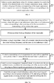
- Table 1 Resonant capacitor of receiver output voltage of receiver output current of receiver output power of receiver input power of transmitter wireless charging efficiency 500nF 19.86V 1A 19.86W 24W 82.8% 203nF 20.41V 1A 20.41W 23.97W 85.2%
- the target capacitance value of the resonant capacitor in the receiver of the electronic device is determined to which the corresponding wireless charging efficiency is superior to the wireless charging efficiency corresponding to the current capacitance value. Afterwards, the resonant capacitor is controlled to adjust from the current capacitance value to the target capacitance value. In the examples, by adjusting the current capacitance value of the resonant capacitor to the target capacitance value, the resonant frequency of the receiver is allowed to be closer to the actual working frequency of the transmitter, which helps improve the wireless charging efficiency and reduce time required for charging the electronic device.
- the examples of the present disclosure further provide an apparatus for improving a wireless charging efficiency.
- the apparatus may be applied to an electronic device supporting wireless charge.
- FIG. 10 is a block diagram illustrating an apparatus for improving a wireless charging efficiency according to an example of the present disclosure. As shown in FIG. 10 , the apparatus 1000 for improving a wireless charging efficiency includes the following modules and units.
- a capacitance value adjusting module 1001 is configured to adjust a current capacitance value of a resonant capacitor in a receiver of the electronic device to a target capacitance value, where a wireless charging efficiency corresponding to the target capacitance value is superior to a wireless charging efficiency corresponding to the current capacitance value.
- the capacitance value adjusting module 1001 includes:
- the open circuit inductance determining sub-module 1101 includes:
- the capacitance value adjusting module 1001 further includes:
- the capacitance value adjusting module 1001 further includes:
- the apparatus for improving a wireless charging efficiency corresponds to the above method of improving a wireless charging efficiency.
- a reference may be made to contents of different examples of the method for specific contents of the apparatus, which will not be repeated herein.
- FIG. 15 is a block diagram illustrating an electronic device 1500 according to an example of the present disclosure.
- the electronic device 1500 may be a mobile phone, a tablet computer, an electronic book reader, a multi-media player, a wearable device, a vehicle-mounted terminal and so on.
- the electronic device 1500 may include one or more of the following components: a processing component 1502, a memory 1504, a power supply component 1506, a multimedia component 1508, an audio component 1510, an input/output (I/O) interface 1512, a sensor component 1514 and a communication component 1516.
- the processing component 1502 usually controls overall operations of the electronic device 1500, such as operations relating to display, a telephone call, data communication, camera operations, and recording operations.
- the processing component 1502 may include one or more processors 1520 for executing instructions to complete all or a part of the steps of the above method.
- the processing component 1502 may include one or more modules to facilitate the interaction between the processing component 1502 and other components.
- the processing component 1502 may include a multimedia module to facilitate the interaction between the multimedia component 1508 and the processing component 1502.
- the processing component 1502 may read executable instructions from a memory to implement steps of the method of improving a wireless charging efficiency according to the above examples.
- the memory 1504 is configured to store different types of data to support operations at the electronic device 1500. Examples of such data include instructions, contact data, phonebook data, messages, pictures, videos, and so on for any application or method that operates on the electronic device 1500.
- the memory 1504 may be implemented by any type of volatile or non-volatile memory devices or a combination thereof, such as a Static Random Access Memory (SRAM), an Electrically Erasable Programmable Read-Only Memory (EEPROM), an Erasable Programmable Read-Only Memory (EPROM), a Programmable Read-Only Memory (PROM), a Read-Only Memory (ROM), a magnetic memory, a flash memory, a magnetic disk or a compact disk.
- SRAM Static Random Access Memory
- EEPROM Electrically Erasable Programmable Read-Only Memory
- EPROM Erasable Programmable Read-Only Memory
- PROM Programmable Read-Only Memory
- ROM Read-Only Memory
- the power supply component 1506 provides power for different components of the electronic device 1500.
- the power supply component 1506 may include a power management system, one or more power supplies, and other components associated with generating, managing and distributing power for the electronic device 1500.
- the power supply component 1506 may further include a receiver used for wireless charge.
- a resonant capacitor in the receiver may be an adjustable capacitor shown in FIG. 3 or 4 .
- the multimedia component 1508 includes a screen providing an output interface between the electronic device 1500 and a user.
- the multimedia component 1508 may include a front-facing camera and/or a rear camera.
- the front-facing camera and/or the rear camera may receive external multimedia data.
- Each of the front-facing camera and the rear camera may be a fixed optical lens system or may be capable of focal length and optical zoom.
- the audio component 1510 is configured to output and/or input an audio signal.
- the audio component 1510 includes a microphone (MIC).
- the microphone is configured to receive an external audio signal.
- the received audio signal may be further stored in the memory 1504 or sent via the communication component 1516.
- the audio component 1510 further includes a speaker for outputting an audio signal.
- the I/O interface 1512 provides an interface between the processing component 1502 and a peripheral interface module.
- the peripheral interface module may be a keyboard, a click wheel, a button, or the like. These buttons may include but not limited to, a home button, a volume button, a start button and a lock button.
- the sensor component 1514 includes one or more sensors for providing a state assessment in different aspects for the electronic device 1500.
- the sensor component 1514 may detect the on/off state of the electronic device 1500, and relative locations of components, for example, the components are a display and a keypad of the electronic device 1500.
- the sensor component 1514 may also detect a position change of the electronic device 1500 or a component of the electronic device 1500, presence or absence of contact of a user with the electronic device 1500, an orientation or acceleration/deceleration of the electronic device 1500 and a temperature change of the electronic device 1500.
- the sensor component 1514 may include a proximity sensor configured to detect presence of a nearby object without any physical contact.
- the sensor component 1514 may further include an optical sensor, such as a CMOS or CCD image sensor used in an imaging application.
- the sensor component 1514 may further include an acceleration sensor, a gyroscope sensor, a magnetic sensor, a pressure sensor, or a temperature sensor.
- the communication component 1516 is configured to facilitate wired or wireless communication between the electronic device 1500 and other devices.
- the electronic device 1500 may access a wireless network based on a communication standard, such as WIFI, 2G or 3G, 4G, 5G, or a combination thereof.
- the communication component 1516 receives a broadcast signal or broadcast-related information from an external broadcast management system via a broadcast channel.
- the communication component 1516 may further include a Near Field Communication (NFC) module to facilitate short-range communications.
- the NFC module may be implemented based on Radio Frequency Identification (RFID) technology, Infrared Data Association (IrDA) technology, Ultra Wide Band (UWB) technology, Bluetooth (BT) technology and other technology.
- RFID Radio Frequency Identification
- IrDA Infrared Data Association
- UWB Ultra Wide Band
- Bluetooth Bluetooth
- the electronic device 1500 may be implemented by one or more of Application-Specific Integrated Circuits (ASIC), Digital Signal Processors (DSP), Digital Signal Processing Devices (DSPD), Programmable Logical Devices (PLD), Field Programmable Gate Arrays (FPGA), controllers, microcontrollers, microprocessors or other electronic elements to perform the above method.
- ASIC Application-Specific Integrated Circuits
- DSP Digital Signal Processors
- DSPD Digital Signal Processing Devices
- PLD Programmable Logical Devices
- FPGA Field Programmable Gate Arrays
- controllers microcontrollers, microprocessors or other electronic elements to perform the above method.
- non-transitory machine readable storage medium including instructions, for example, the memory 1504 including instructions.
- the above instructions may be executed by the processor 1520 of the electronic device 1500 to complete the above method.
- the non-transitory computer readable storage medium may be a Read-Only Memory (ROM), a Random Access Memory (RAM), a CD-ROM, a magnetic tape, a floppy disk, and optical data storage device and so on.
Abstract
Description
- The present disclosure relates to the field of wireless charging technology, and in particular to a method of improving a wireless charging efficiency, an electronic device, an apparatus and a storage medium.
- At present, in a wireless charging solution of Qi protocol (a wireless charging protocol stipulated by Wireless Power Consortium (WPC)), it is stipulated that a capacitance value of a resonant capacitor in a receiver of an electronic device is a fixed value, i.e. 400nF or 500nF in a case of a resonant frequency of 100kHz.
- However, because a transmitter of a wireless charging device adjusts an actual working frequency (for example, 110kHz∼148kHz) according to its output voltage, a resonant frequency of the receiver is not matched with the actual working frequency of the transmitter. In this case, the resonant capacitor of the receiver does not work at an optimal charging efficiency.
- The present disclosure provides a method of improving a wireless charging efficiency, an electronic device, an apparatus and a storage medium to solve shortages of the related art.
- According to a first aspect of the present disclosure, a method of improving a wireless charging efficiency is provided. The method may be applicable to an electronic device having a wireless charging function. The method includes: adjusting a current capacitance value of a resonant capacitor of a receiver in the electronic device to a target capacitance value, where a wireless charging efficiency corresponding to the target capacitance value is superior to a wireless charging efficiency corresponding to the current capacitance value.
- According to a second aspect of the present disclosure, an apparatus for improving a wireless charging efficiency. The apparatus may be applicable to an electronic device having a wireless charging function. The apparatus includes a capacitance value adjusting module, configured to adjust a current capacitance value of a resonant capacitor in a receiver of the electronic device to a target capacitance value, where a wireless charging efficiency corresponding to the target capacitance value is superior to a wireless charging efficiency corresponding to the current capacitance value.
- According to a third aspect of the present disclosure, an electronic device is provided. The electronic device includes a receiver used for wireless charge where a resonant capacitor is disposed in the receiver and a receiving coil is disposed in the receiver and connected with the resonant capacitor; one or more processors connected with the resonant capacitor; and a memory storing executable instructions. When reading the executable instructions from the memory, the processors are configured to adjust a current capacitance value of the resonant capacitor to a target capacitance value, where a wireless charging efficiency corresponding to the target capacitance value is superior to a wireless charging efficiency corresponding to the current capacitance value.
- According to a fourth aspect of the present disclosure, a machine readable storage medium storing machine executable instructions is provided. The instructions are executed by a processor to perform the following operations: adjusting a current capacitance value of a resonant capacitor of a receiver of an electronic device to a target capacitance value, where a wireless charging efficiency corresponding to the target capacitance value is superior to a wireless charging efficiency corresponding to the current capacitance value.
- It is understood that the above general descriptions and subsequent detailed descriptions are merely illustrative and explanatory and shall not be intended to limit the present disclosure.
- The accompanying drawings, which are incorporated in and constitute a part of the present description, illustrate examples consistent with the present disclosure and serve to explain the principles of the present disclosure together with the description.
-
FIG. 1 is a wireless charging circuit in related art. -
FIG. 2 illustrates a model of a wireless charging circuit according to an example of the present disclosure. -
FIG. 3 is a schematic diagram illustrating a variable capacitor according to an example of the present disclosure. -
FIG. 4 is a schematic diagram illustrating a resonant capacitor formed by connecting a plurality of capacitor branches in parallel according to an example of the present disclosure. -
FIG. 5 is a flowchart illustrating a method of improving a wireless charging efficiency according to an example of the present disclosure. -
FIG. 6 is a flowchart of obtaining a target capacitance value according to an example of the present disclosure. -
FIG. 7A is a flowchart of obtaining an open circuit inductance value according to an example of the present disclosure. -
FIG. 7B is a schematic diagram illustrating a signal of damping oscillation according to an example of the present disclosure. -
FIG. 8 is another flowchart of obtaining a target capacitance value according to an example of the present disclosure. -
FIG. 9 is yet another flowchart of obtaining a target capacitance value according to an example of the present disclosure. -
FIG. 10 is a block diagram illustrating an apparatus for improving a wireless charging efficiency according to an example of the present disclosure. -
FIG. 11 illustrates an example for the capacitance value adjusting module. -
FIG. 12 illustrates an example for the open circuit inductance determining sub-module. -
FIG. 13 illustrates an example for the capacitance value adjusting module. -
FIG. 14 illustrates an example for the capacitance value adjusting module. -
FIG. 15 is a block diagram illustrating an electronic device according to an example of the present disclosure. - Examples will be described in detail herein with the examples thereof expressed in the drawings. When the following descriptions involve the drawings, like numerals in different drawings represent like or similar elements unless stated otherwise. The implementations described in the following examples do not represent all implementations consistent with the present disclosure. On the contrary, they are examples of an apparatus and a method consistent with some aspects of the present disclosure described in detail in the appended claims.
- At present, in a wireless charging solution of Qi protocol (a wireless charging protocol stipulated by wireless power consortium), it is stipulated that a capacitance value of a resonant capacitor in a receiver of an electronic device is a fixed value, i.e. 400nF or 500nF in a case of a resonant frequency of 100kHz.
FIG. 1 is a wireless charging circuit in related art. As shown inFIG. 1 , coil L7 is a transmitting coil in a transmitter of a wireless charging device, capacitor C6 is a transmitting capacitor in the transmitter, coil L8 is a receiving coil in the receiver, capacitor C7 is a resonant capacitor in the receiver, where the capacitor C7 is of fixed value, for example, 400nF or 500nF. - However, because the transmitter adjusts an actual working frequency (for example, 110kHz∼148kHz) according to its output voltage, a resonant frequency of the receiver is not matched with the actual working frequency of the transmitter. In this case, the resonant capacitor of the receiver does not work at an optimal charging efficiency. Further, if positions that the transmitting coil in the transmitter is placed on the receiving coil in the receiver are different, an inductance value of the receiving coil in the receiver is changed. In this case, the resonant frequency of the receiver is not matched with the working frequency of the transmitter, further reducing wireless charging efficiency.
- To overcome the above problem, the examples of the present disclosure provide a wireless charging circuit.
FIG. 2 is a model of a wireless charging circuit according to an example of the present disclosure. As shown inFIG. 2 , the transmitter includes a transmitting capacitor Cs_pri, an equivalent resistor Resr_11 and a transmitting coil L11. The receiver includes a resonant capacitor Cs_sec, an equivalent resistor Resr_22, and a receiving coil L22. The receiver further includes a load RL of the electronic device. A mutual inductance between the transmitting coil L11 and the receiving coil L22 is

- Based on the formula, it is deduced that, in a case of

- In an example of the present disclosure, in combination with the above formula (2), the resonant capacitor of the receiver is configured as an adjustable capacitor. In this case, the wireless charging efficiency of the receiver may be adjusted by adjusting the capacitance value of the resonant capacitor in the receiver.
- In an example, the resonant capacitor in the receiver may be a variable capacitor, which is a capacitor whose capacitance may be intentionally and repeatedly changed mechanically or electronically. As shown in
FIG. 3 , the variable capacitor includes an input end In, an output end Out, and a control end Con. In combination withFIGS. 2 and 3 , the input end In of the variable capacitor is connected with the equivalent resistor Resr_22, and the output end Out is connected with the load RL of the electronic device. The control end Con is connected with a processor of the electronic device, or coupled with a controller of a wireless charging device. After determining a target capacitance value of the resonant capacitor, the processor or the controller may input a target voltage corresponding to the target capacitance value to the control end Con of the variable capacitor so that the capacitance value of the variable capacitor changes to the target capacitance value. - In another example, the resonant capacitor in the receiver includes a plurality of capacitor branches connected in parallel. The number of the capacitor branches may be set according to the specific application scenario. As shown in
FIG. 4 , each capacitor branch includes one capacitor C and one controllable switch K connected in series. The control end Con of the plurality of capacitor branches connected in parallel is connected with the processor. In this case, the processor may connect in parallel all or part of the capacitors C1-C5 between the input end In and the output end Out by controlling each switch of the controller switches K(K1-K5) to turn off or on, thereby adjusting the resonant capacitor. - In another example, the resonant capacitor in the receiver may also be a mechanically adjustable capacitor. The mechanically adjustable capacitor may be adjusted by controlling a drive apparatus, thereby adjusting the resonant capacitor.
- In the case of the above receiver, the examples of the present disclosure provide a method of improving a wireless charging efficiency. The method may be applied to a processor of an electronic device.
FIG. 5 is a flowchart illustrating a method of improving a wireless charging efficiency according to an example of the present disclosure. As shown inFIG. 5 , the method of improving a wireless charging efficiency may includestep 501. - At
step 501, a current capacitance value of a resonant capacitor in a receiver of the electronic device is adjusted to a target capacitance value, where a wireless charging efficiency corresponding to the target capacitance value is superior to a wireless charging efficiency corresponding to the current capacitance value. - In the example, the processor of the electronic device may determine the target capacitance value of the resonant capacitor in the receiver of the electronic device in the following manners.
- In the first manner, as shown in
FIG. 6 , the processor firstly calculates an open circuit inductance value of the receiving coil L22 (corresponding to step 601). With continuous reference toFIG. 2 , the open circuit inductance value is an inductance value corresponding to the receiving coil L22 in the receiver when the transmitting coil L11 is in an open-circuit state. In other words, the open circuit inductance value is an inductance value corresponding to the receiving coil L22 in the receiver when the current i1 is zero. - As shown in
FIG. 7A , the open circuit inductance value may be calculated as follows: - After the transmitter is placed on the receiver, the processor may control the transmitting coil to open within a specified time period (corresponding to step 701), or the transmitter and the receiver may negotiate to enable the transmitting coil in the transmitter to maintain open within a specified time period. Afterwards, the processor may control a power management integrated circuit (PMIC) of the electronic device to perform reverse excitation for the receiving coil. In this way, damping oscillation signals are generated on the receiving coil (corresponding to step 702). The damping oscillation signals are sinusoidal periodic signals. Afterwards, the processor may detect amplitudes of the damping oscillation signals generated on the receiving coil, select two designated amplitudes and then calculate the open circuit inductance value L of the receiving coil L22 according to a time interval Δt between the two designated amplitudes (corresponding to step 703). The two designated amplitudes may be two preset amplitudes th0 and th1, which is specifically indicated in
FIG. 7B . Further, because position that the transmitter is placed on the receiver is different each time, calculation result of the open circuit inductance value L is different each time. - With continuous reference to
FIG. 6 , the processor may obtain the actual working frequency of the transmitter (corresponding to step 602). It is noted that the transmitter may adjust its actual working frequency in real time according to an output voltage of the transmitting coil. After the actual working frequency is determined, the processor may interact with the transmitter to obtain the actual working frequency of the transmitter. In addition, the sequence of performingsteps - With continuous reference to
FIG. 6 , in combination with the formula (2), the processor may determine the target capacitance value of the resonant capacitor according to the actual working frequency of the transmitter and the open circuit inductance value of the receiving coil (corresponding to step 603). - In the second manner, as shown in
FIG. 8 , the processor may adjust the current capacitance value of the resonant capacitor by a preset step length to obtain an adjusted capacitance value (corresponding to step 801). For example, the resonant capacitor may be an adjustable capacitor. In this case, the processor may increase a voltage by 0.1V each time on the basis of a current control voltage, so that the current capacitance value of the resonant capacitor becomes larger. For another example, the resonant capacitor is a capacitor formed by connecting a plurality of capacitor branches in parallel. In this case, the processor may turn off one controllable switch sequentially, so that the corresponding capacitor branch is removed from the resonant capacitor or the processor may turn on one controllable switch sequentially, so that the corresponding capacitor branch is incorporated into the resonant capacitor to change the current capacitance value of the resonant capacitor. Then, the processor may determine a wireless charging efficiency corresponding to the adjusted capacitance value (corresponding to step 802). Afterwards, the processor may determine whether the wireless charging efficiency exceeds a wireless charging efficiency threshold. If yes, it is determined the adjusted capacitance value is the target capacitance value (corresponding to step 803). If not, the processor continues to perform steps 801-803 until the wireless charging efficiency exceeds the wireless charging efficiency threshold. - In the third manner, as shown in
FIG. 9 , the processor may dynamically adjust the current capacitance value of the resonant capacitor so that the wireless charging efficiency of the receiver (the wireless charging efficiency corresponding to the current capacitance value) continuously increases until the wireless charging efficiency decreases or remains unchanged (corresponding to step 901). Afterwards, the processor determines a corresponding current capacitance value as the target capacitance value of the resonant capacitor when the wireless charging efficiency starts to decrease or starts to remain unchanged (corresponding to step 902). In other words, the processor may obtain a corresponding wireless charging efficiency curve by adjusting the capacitance value of the resonant capacitor from the minimum to the maximum, and determine the capacitance value corresponding to an inflexion point on the wireless charging efficiency curve as the target capacitance value of the resonant capacitor. - In the example, the processor or a controller may control the resonant capacitor to adjust from the current capacitance value to the target capacitance value, so that the wireless charging efficiency of the receiver exceeds the wireless charging efficiency threshold and even is the optimal wireless charging efficiency.
- In an example, the resonant capacitor in the receiver is of a fixed value of 500nF. Results shown in Table 1 may be obtained by adjusting the capacitance value of the resonant capacitor by the method of improving a wireless charging efficiency according to the examples of the present disclosure.
Table 1 Resonant capacitor of receiver output voltage of receiver output current of receiver output power of receiver input power of transmitter wireless charging efficiency 500nF 19.86V 1A 19.86W 24W 82.8% 203nF 20.41V 1A 20.41W 23.97W 85.2% - In the wireless charging process, analysis shows that when the resonant capacitor of the receiver is 203nF, the efficiency is the highest. Compared with the resonant capacitor of 500nF, the wireless charging efficiency is increased by 2.8%.
- In the examples of the present disclosure, the target capacitance value of the resonant capacitor in the receiver of the electronic device is determined to which the corresponding wireless charging efficiency is superior to the wireless charging efficiency corresponding to the current capacitance value. Afterwards, the resonant capacitor is controlled to adjust from the current capacitance value to the target capacitance value. In the examples, by adjusting the current capacitance value of the resonant capacitor to the target capacitance value, the resonant frequency of the receiver is allowed to be closer to the actual working frequency of the transmitter, which helps improve the wireless charging efficiency and reduce time required for charging the electronic device.
- Based on the method of improving a wireless charging efficiency according to some examples of the present disclosure, the examples of the present disclosure further provide an apparatus for improving a wireless charging efficiency. The apparatus may be applied to an electronic device supporting wireless charge.
FIG. 10 is a block diagram illustrating an apparatus for improving a wireless charging efficiency according to an example of the present disclosure. As shown inFIG. 10 , theapparatus 1000 for improving a wireless charging efficiency includes the following modules and units. - A capacitance
value adjusting module 1001 is configured to adjust a current capacitance value of a resonant capacitor in a receiver of the electronic device to a target capacitance value, where a wireless charging efficiency corresponding to the target capacitance value is superior to a wireless charging efficiency corresponding to the current capacitance value. - As shown in
FIG. 11 , based on theapparatus 1000 for improving a wireless charging efficiency shown inFIG. 10 , the capacitancevalue adjusting module 1001 includes: - an open circuit inductance determining sub-module 1101, configured to determine an open circuit inductance value in the receiver, where the open circuit inductance value is an inductance value corresponding to a receiving coil in the receiver when a transmitting coil in a transmitter of a wireless charging device is in an open-circuit state;
- a working frequency obtaining sub-module 1102, configured to obtain an actual working frequency of the transmitter; and
- a capacitance value determining sub-module 1103, configured to determine the target capacitance value of the resonant capacitor according to the actual working frequency and the open circuit inductance value.
- As shown in
FIG. 12 , based on theapparatus 1000 for improving a wireless charging efficiency shown inFIG. 11 , the open circuit inductance determining sub-module 1101 includes: - an open
circuit controlling unit 1201, configured to control the transmitting coil to open within a specified time period when it is detected the transmitter is placed on the receiver; - a coil
exciting unit 1202, configured to control a Power Management Integrated Circuit of the electronic device to perform reverse excitation for the receiving coil, so that damping oscillation signals are generated on the receiving coil; and - an open circuit
inductance determining unit 1203, configured to determine the open circuit inductance value of the receiving coil according to two designated amplitudes of the damping oscillation signals on the receiving coil and a time interval between the two designated amplitudes. - As shown in
FIG. 13 , based on theapparatus 1000 for improving a wireless charging efficiency shown inFIG. 10 , the capacitancevalue adjusting module 1001 further includes: - a current capacitance adjusting sub-module 1301, configured to obtain an adjusted capacitance value by adjusting the current capacitance value of the resonant capacitor by a preset step length sequentially;
- a charging efficiency determining sub-module 1302, configured to determine a wireless charging efficiency corresponding to the adjusted capacitance value; and
- a capacitance value determining sub-module 1303, configured to determine the adjusted capacitance value as a target capacitance value until the wireless charging efficiency exceeds a preset wireless charging efficiency threshold.
- As shown in
FIG. 14 , based on theapparatus 1000 for improving a wireless charging efficiency shown inFIG. 10 , the capacitancevalue adjusting module 1001 further includes: - a capacitance value adjusting sub-module 1401, configured to dynamically adjust the current capacitance value of the resonant capacitor to obtain intermediate capacitance values, so that the corresponding wireless charging efficiency continuously increases until the wireless charging efficiency decreases or remains unchanged;
- a capacitance value determining sub-module 1402, configured to determine a corresponding intermediate capacitance value as the target capacitance value of the resonant capacitor until the wireless charging efficiency starts to decrease or starts to remain unchanged.
- It is understood that the apparatus for improving a wireless charging efficiency according to the examples of the present disclosure corresponds to the above method of improving a wireless charging efficiency. A reference may be made to contents of different examples of the method for specific contents of the apparatus, which will not be repeated herein.
-
FIG. 15 is a block diagram illustrating anelectronic device 1500 according to an example of the present disclosure. For example, theelectronic device 1500 may be a mobile phone, a tablet computer, an electronic book reader, a multi-media player, a wearable device, a vehicle-mounted terminal and so on. - As shown in
FIG. 15 , theelectronic device 1500 may include one or more of the following components: aprocessing component 1502, amemory 1504, apower supply component 1506, amultimedia component 1508, anaudio component 1510, an input/output (I/O)interface 1512, asensor component 1514 and acommunication component 1516. - The
processing component 1502 usually controls overall operations of theelectronic device 1500, such as operations relating to display, a telephone call, data communication, camera operations, and recording operations. Theprocessing component 1502 may include one ormore processors 1520 for executing instructions to complete all or a part of the steps of the above method. In addition, theprocessing component 1502 may include one or more modules to facilitate the interaction between theprocessing component 1502 and other components. For example, theprocessing component 1502 may include a multimedia module to facilitate the interaction between themultimedia component 1508 and theprocessing component 1502. For another example, theprocessing component 1502 may read executable instructions from a memory to implement steps of the method of improving a wireless charging efficiency according to the above examples. - The
memory 1504 is configured to store different types of data to support operations at theelectronic device 1500. Examples of such data include instructions, contact data, phonebook data, messages, pictures, videos, and so on for any application or method that operates on theelectronic device 1500. Thememory 1504 may be implemented by any type of volatile or non-volatile memory devices or a combination thereof, such as a Static Random Access Memory (SRAM), an Electrically Erasable Programmable Read-Only Memory (EEPROM), an Erasable Programmable Read-Only Memory (EPROM), a Programmable Read-Only Memory (PROM), a Read-Only Memory (ROM), a magnetic memory, a flash memory, a magnetic disk or a compact disk. - The
power supply component 1506 provides power for different components of theelectronic device 1500. Thepower supply component 1506 may include a power management system, one or more power supplies, and other components associated with generating, managing and distributing power for theelectronic device 1500. Thepower supply component 1506 may further include a receiver used for wireless charge. A resonant capacitor in the receiver may be an adjustable capacitor shown inFIG. 3 or 4 . - The
multimedia component 1508 includes a screen providing an output interface between theelectronic device 1500 and a user. In some examples, themultimedia component 1508 may include a front-facing camera and/or a rear camera. When theelectronic device 1500 is in an operating mode, such as in a shooting mode or a video mode, the front-facing camera and/or the rear camera may receive external multimedia data. Each of the front-facing camera and the rear camera may be a fixed optical lens system or may be capable of focal length and optical zoom. - The
audio component 1510 is configured to output and/or input an audio signal. For example, theaudio component 1510 includes a microphone (MIC). When theelectronic device 1500 is in an operating mode, for example, in a call mode, a recording mode or a voice recognition mode, the microphone is configured to receive an external audio signal. The received audio signal may be further stored in thememory 1504 or sent via thecommunication component 1516. In some examples, theaudio component 1510 further includes a speaker for outputting an audio signal. - The I/
O interface 1512 provides an interface between theprocessing component 1502 and a peripheral interface module. The peripheral interface module may be a keyboard, a click wheel, a button, or the like. These buttons may include but not limited to, a home button, a volume button, a start button and a lock button. - The
sensor component 1514 includes one or more sensors for providing a state assessment in different aspects for theelectronic device 1500. For example, thesensor component 1514 may detect the on/off state of theelectronic device 1500, and relative locations of components, for example, the components are a display and a keypad of the electronic device 1500.Thesensor component 1514 may also detect a position change of theelectronic device 1500 or a component of theelectronic device 1500, presence or absence of contact of a user with theelectronic device 1500, an orientation or acceleration/deceleration of theelectronic device 1500 and a temperature change of theelectronic device 1500. Thesensor component 1514 may include a proximity sensor configured to detect presence of a nearby object without any physical contact. Thesensor component 1514 may further include an optical sensor, such as a CMOS or CCD image sensor used in an imaging application. In some examples, thesensor component 1514 may further include an acceleration sensor, a gyroscope sensor, a magnetic sensor, a pressure sensor, or a temperature sensor. - The
communication component 1516 is configured to facilitate wired or wireless communication between theelectronic device 1500 and other devices. Theelectronic device 1500 may access a wireless network based on a communication standard, such as WIFI, 2G or 3G, 4G, 5G, or a combination thereof. In an example, thecommunication component 1516 receives a broadcast signal or broadcast-related information from an external broadcast management system via a broadcast channel. In an example, thecommunication component 1516 may further include a Near Field Communication (NFC) module to facilitate short-range communications. For example, the NFC module may be implemented based on Radio Frequency Identification (RFID) technology, Infrared Data Association (IrDA) technology, Ultra Wide Band (UWB) technology, Bluetooth (BT) technology and other technology. - In an example, the
electronic device 1500 may be implemented by one or more of Application-Specific Integrated Circuits (ASIC), Digital Signal Processors (DSP), Digital Signal Processing Devices (DSPD), Programmable Logical Devices (PLD), Field Programmable Gate Arrays (FPGA), controllers, microcontrollers, microprocessors or other electronic elements to perform the above method. - In an example, there is further provided a non-transitory machine readable storage medium including instructions, for example, the
memory 1504 including instructions. The above instructions may be executed by theprocessor 1520 of theelectronic device 1500 to complete the above method. For example, the non-transitory computer readable storage medium may be a Read-Only Memory (ROM), a Random Access Memory (RAM), a CD-ROM, a magnetic tape, a floppy disk, and optical data storage device and so on. - After considering the specification and practicing the present disclosure, the persons of skill in the art may easily conceive of other implementations of the present disclosure. The present disclosure is intended to include any variations, uses and adaptive changes of the present disclosure. These variations, uses and adaptive changes follow the general principle of the present disclosure and include common knowledge or conventional technical means in the prior art not disclosed in the present disclosure. The specification and examples herein are intended to be illustrative only and the scope of the present disclosure are indicated by the claims.
- It is to be understood that the present disclosure is not limited to the precise structures described above and shown in the accompanying drawings and may be modified or changed without departing from the scope of the present disclosure. The scope of protection of the present disclosure is limited only by the appended claims.
Claims (14)
- A method of improving a wireless charging efficiency, the method being applicable to an electronic device supporting wireless charge, and comprising:
adjusting a current capacitance value of a resonant capacitor (C7) in a receiver of the electronic device to a target capacitance value, wherein a wireless charging efficiency corresponding to the target capacitance value is superior to a wireless charging efficiency corresponding to the current capacitance value. - The method according to claim 1, further comprising:determining an open circuit inductance value in the receiver, wherein the open circuit inductance value is an inductance value corresponding to a receiving coil (L22) in the receiver when a transmitting coil (L11) in a transmitter of a wireless charging device for charging the electronic device is in an open-circuit state;obtaining an actual working frequency of the transmitter; anddetermining the target capacitance value of the resonant capacitor according to the actual working frequency and the open circuit inductance value.
- The method according to claim 2, wherein determining the open circuit inductance value in the receiver comprises:when it is detected that the transmitter is placed on the receiver, controlling the transmitting coil to open within a specified time period;controlling a power management integrated circuit of the electronic device to perform reverse excitation for the receiving coil so that damping oscillation signals are generated on the receiving coil; anddetermining the open circuit inductance value according to two amplitudes of the damping oscillation signals on the receiving coil and a time interval between the two amplitudes.
- The method according to any preceding claim, wherein adjusting the current capacitance value of the resonant capacitor in the receiver of the electronic device to the target capacitance value comprises:obtaining an adjusted capacitance value by adjusting the current capacitance value of the resonant capacitor by a set step length sequentially;determining a wireless charging efficiency corresponding to the adjusted capacitance value; andin response to determining that the wireless charging efficiency exceeds a preset wireless charging efficiency threshold, determining the adjusted capacitance value as the target capacitance value.
- The method according to any of claims 1 to 3, wherein adjusting the current capacitance value of the resonant capacitor in the receiver of the electronic device to the target capacitance value comprises:dynamically adjusting the current capacitance value of the resonant capacitor to obtain intermediate capacitance values so that the wireless charging efficiency continuously increases until the wireless charging efficiency decreases or remains unchanged; anddetermining a corresponding intermediate capacitance value as the target capacitance value of the resonant capacitor when the wireless charging efficiency starts to decrease or starts to remain unchanged.
- An apparatus for improving a wireless charging efficiency, the apparatus being applicable to an electronic device supporting wireless charge, comprising:
a capacitance value adjusting module (1001), configured to adjust a current capacitance value of a resonant capacitor (C7) in a receiver of the electronic device to a target capacitance value, where a wireless charging efficiency corresponding to the target capacitance value is superior to a wireless charging efficiency corresponding to the current capacitance value. - The apparatus according to claim 6, the capacitance value adjusting module comprises:an open circuit inductance determining sub-module (1101), configured to determine an open circuit inductance value in the receiver, where the open circuit inductance value is an inductance value corresponding to a receiving coil in the receiver when a transmitting coil in a transmitter of a wireless charging device is in an open-circuit state;a working frequency obtaining sub-module (1102), configured to obtain an actual working frequency of the transmitter; anda capacitance value determining sub-module (1103), configured to determine the target capacitance value of the resonant capacitor according to the actual working frequency and the open circuit inductance value.
- The apparatus according to claim 7, the open circuit inductance determining sub-module comprises:an open circuit controlling unit (1201), configured to control the transmitting coil to open within a specified time period when it is detected the transmitter is placed on the receiver;a coil exciting unit (1202), configured to control a Power Management Integrated Circuit of the electronic device to perform reverse excitation for the receiving coil, so that damping oscillation signals are generated on the receiving coil; andan open circuit inductance determining unit (1203), configured to determine the open circuit inductance value of the receiving coil according to two designated amplitudes of the damping oscillation signals on the receiving coil and a time interval between the two designated amplitudes.
- The apparatus according to claim 6, the capacitance value adjusting module further comprises:a current capacitance adjusting sub-module (1301), configured to obtain an adjusted capacitance value by adjusting the current capacitance value of the resonant capacitor by a preset step length sequentially;a charging efficiency determining sub-module (1302), configured to determine a wireless charging efficiency corresponding to the adjusted capacitance value; anda capacitance value determining sub-module (1303), configured to determine the adjusted capacitance value as a target capacitance value until the wireless charging efficiency exceeds a preset wireless charging efficiency threshold.
- The apparatus according to claim 6, the capacitance value adjusting module further comprises:a capacitance value adjusting sub-module (1401), configured to dynamically adjust the current capacitance value of the resonant capacitor to obtain intermediate capacitance values, so that the corresponding wireless charging efficiency continuously increases until the wireless charging efficiency decreases or remains unchanged;a capacitance value determining sub-module (1402), configured to determine a corresponding intermediate capacitance value as the target capacitance value of the resonant capacitor until the wireless charging efficiency starts to decrease or starts to remain unchanged.
- An electronic device, comprising:a receiver for wireless charge where a resonant capacitor is disposed in the receiver and a receiving coil is disposed in the receiver and connected with the resonant capacitor;one or more processors (1502) connected with the resonant capacitor; anda memory (1504) storing executable instructions;wherein when reading executable instructions from the memory, the processors are caused to perform operations in accordance with the method of any of claims 1-5.
- The electronic device according to claim 11, wherein the resonant capacitor comprises a variable capacitor.
- The electronic device according to claim 11, wherein,
the resonant capacitor comprises a plurality of capacitor branches connected in parallel;
each of the capacitor branches comprises a capacitor and a controllable switch connected in series; and the controllable switch is connected with the processors. - A machine readable storage medium storing machine executable instructions, wherein the instructions are executed by a processor to perform operations in accordance with the method of any of claims 1-5.
Applications Claiming Priority (1)
| Application Number | Priority Date | Filing Date | Title |
|---|---|---|---|
| CN201910237992.2A CN111756119A (en) | 2019-03-27 | 2019-03-27 | Method and device for improving wireless charging efficiency and electronic equipment |
Publications (2)
| Publication Number | Publication Date |
|---|---|
| EP3716443A1 true EP3716443A1 (en) | 2020-09-30 |
| EP3716443B1 EP3716443B1 (en) | 2023-08-16 |
Family
ID=68762489
Family Applications (1)
| Application Number | Title | Priority Date | Filing Date |
|---|---|---|---|
| EP19212715.7A Active EP3716443B1 (en) | 2019-03-27 | 2019-11-29 | Method of improving wireless charging efficiency, electronic device, apparatus and storage medium |
Country Status (3)
| Country | Link |
|---|---|
| US (1) | US11264824B2 (en) |
| EP (1) | EP3716443B1 (en) |
| CN (1) | CN111756119A (en) |
Families Citing this family (18)
| Publication number | Priority date | Publication date | Assignee | Title |
|---|---|---|---|---|
| US11005308B1 (en) | 2020-06-28 | 2021-05-11 | Nucurrent, Inc. | Wireless power transmitter for high fidelity communications and high power transfer |
| US11476724B2 (en) | 2020-06-28 | 2022-10-18 | Nucurrent, Inc. | Higher power high frequency wireless power transfer system |
| US11476725B2 (en) | 2020-06-28 | 2022-10-18 | Nucurrent, Inc. | Wireless power transmitter for high fidelity communications and high power transfer |
| US11469626B2 (en) | 2020-06-28 | 2022-10-11 | Nucurrent, Inc. | Wireless power receiver for receiving high power high frequency transfer |
| US11404918B2 (en) | 2020-07-21 | 2022-08-02 | Nucurrent, Inc. | Wireless charging in eyewear with enhanced positional freedom |
| US11711112B2 (en) | 2021-01-28 | 2023-07-25 | Nucurrent, Inc. | Wireless power transmission systems and methods with selective signal damping active mode |
| US11722179B2 (en) | 2021-01-28 | 2023-08-08 | Nucurrent, Inc. | Wireless power transmission systems and methods for selectively signal damping for enhanced communications fidelity |
| US11476897B2 (en) | 2021-01-28 | 2022-10-18 | Nucurrent, Inc. | Wireless power transmitter for high fidelity communications at high power transfer |
| EP4285463A1 (en) * | 2021-01-28 | 2023-12-06 | NuCurrent, Inc. | Wireless power transmission systems and methods for selectively signal damping for enhanced communications fidelity |
| US11483032B2 (en) | 2021-01-28 | 2022-10-25 | Nucurrent, Inc. | Wireless power transmission systems and methods with selective signal damping at periodic active mode windows |
| US11695449B2 (en) | 2021-01-28 | 2023-07-04 | Nucurrent, Inc. | Wireless power transmission systems and methods with signal damping operating modes |
| US11489555B2 (en) | 2021-01-28 | 2022-11-01 | Nucurrent, Inc. | Wireless power transmitter for high fidelity communications with amplitude shift keying |
| WO2023023356A1 (en) * | 2021-08-19 | 2023-02-23 | Nucurrent, Inc. | Wireless power transmitter for high fidelity communications and high power transfer |
| CN114123436B (en) * | 2022-01-25 | 2023-04-07 | 合肥有感科技有限责任公司 | Inductance deviation self-adaptive wireless charging method |
| CN114679197A (en) * | 2022-03-02 | 2022-06-28 | 维沃移动通信有限公司 | Radio frequency circuit, capacitance value control method thereof and electronic equipment |
| CN114661090A (en) * | 2022-05-19 | 2022-06-24 | 深之蓝(天津)水下智能科技有限公司 | Method and system for self-adaptively acquiring matching capacitance value |
| CN116148584B (en) * | 2023-04-18 | 2023-09-01 | 紫光同芯微电子有限公司 | Wireless charging parameter testing method, device, equipment and medium |
| CN117691770A (en) * | 2024-02-04 | 2024-03-12 | 荣耀终端有限公司 | Wireless charging method and electronic equipment |
Citations (2)
| Publication number | Priority date | Publication date | Assignee | Title |
|---|---|---|---|---|
| US20160248275A1 (en) * | 2013-12-10 | 2016-08-25 | The Chugoku Electric Power Co., Inc. | Power receiving device and power feeding system |
| US20170346343A1 (en) * | 2016-05-27 | 2017-11-30 | Witricity Corporation | Voltage Regulation in Wireless Power Receivers |
Family Cites Families (6)
| Publication number | Priority date | Publication date | Assignee | Title |
|---|---|---|---|---|
| KR20150050027A (en) * | 2013-10-31 | 2015-05-08 | 삼성전기주식회사 | Wireless charging device and controlling method thereof |
| CN104659930B (en) * | 2014-08-13 | 2016-05-11 | 武汉泰可电气股份有限公司 | Radio energy receiving equipment and the method for adaptive frequency |
| US10491027B2 (en) * | 2016-04-01 | 2019-11-26 | Intel Corporation | Wireless power transmission |
| US10063087B2 (en) * | 2016-04-26 | 2018-08-28 | Nxp B.V. | Automatic tuning of resonance-based wireless charging receiver |
| TWI662760B (en) * | 2017-08-21 | 2019-06-11 | 國立交通大學 | Resonant magnetic coupling wireless power transfer system with calibration capability of its inductor-capacitor resonant frequencies |
| CN109494888A (en) * | 2018-11-27 | 2019-03-19 | 努比亚技术有限公司 | Wireless charging receiving terminal, terminal, system, method and readable storage medium storing program for executing |
-
2019
- 2019-03-27 CN CN201910237992.2A patent/CN111756119A/en active Pending
- 2019-11-08 US US16/679,135 patent/US11264824B2/en active Active
- 2019-11-29 EP EP19212715.7A patent/EP3716443B1/en active Active
Patent Citations (2)
| Publication number | Priority date | Publication date | Assignee | Title |
|---|---|---|---|---|
| US20160248275A1 (en) * | 2013-12-10 | 2016-08-25 | The Chugoku Electric Power Co., Inc. | Power receiving device and power feeding system |
| US20170346343A1 (en) * | 2016-05-27 | 2017-11-30 | Witricity Corporation | Voltage Regulation in Wireless Power Receivers |
Also Published As
| Publication number | Publication date |
|---|---|
| CN111756119A (en) | 2020-10-09 |
| US20200313454A1 (en) | 2020-10-01 |
| EP3716443B1 (en) | 2023-08-16 |
| US11264824B2 (en) | 2022-03-01 |
Similar Documents
| Publication | Publication Date | Title |
|---|---|---|
| EP3716443A1 (en) | Method of improving wireless charging efficiency, electronic device, apparatus and storage medium | |
| EP3316473B1 (en) | Method and device for controlling vibration of motor | |
| CN104503671B (en) | The driving control method and device of electronic Self-Balancing vehicle | |
| WO2017071093A1 (en) | Electronic device control method and apparatus | |
| US20180375209A1 (en) | Antenna and electronic device | |
| CN107482710B (en) | Wireless charging method and terminal | |
| CN104683691B (en) | Image pickup method, device and equipment | |
| CN109905812B (en) | Input power control method and device and terminal equipment | |
| US20200374847A1 (en) | Method and apparatus for configuring information, base station and user equipment | |
| KR20160142217A (en) | Method and device of optimizing sound signal | |
| CN105225647A (en) | Luminance regulating method and device | |
| CN105513104A (en) | Picture taking method, device and system | |
| CN107834205A (en) | Anneta module, electronic equipment and the method for controlling the electronic device works frequency | |
| CN109409235B (en) | Image recognition method and device, electronic equipment and computer readable storage medium | |
| EP3961848A1 (en) | Charging control method and apparatus, electronic device and storage medium | |
| CN111934382B (en) | Charging method, charging device and storage medium | |
| EP3016236A1 (en) | Power supply circuit and electronic equipment | |
| CN105357444A (en) | Focusing method and device | |
| CN105430567B (en) | Vehicle whistle volume adjusting method and device | |
| CN113972703A (en) | Wireless charging method, device, terminal and storage medium | |
| CN106101441A (en) | Terminal control method and device | |
| CN114900613A (en) | Control method, intelligent terminal and storage medium | |
| CN108429312A (en) | Charge control method and device | |
| CN109450032B (en) | Wireless charging processing method, device and equipment | |
| CN112311035B (en) | Charge control method, charge control device, and readable storage medium |
Legal Events
| Date | Code | Title | Description |
|---|---|---|---|
| PUAI | Public reference made under article 153(3) epc to a published international application that has entered the european phase |
Free format text: ORIGINAL CODE: 0009012 |
|
| STAA | Information on the status of an ep patent application or granted ep patent |
Free format text: STATUS: THE APPLICATION HAS BEEN PUBLISHED |
|
| AK | Designated contracting states |
Kind code of ref document: A1 Designated state(s): AL AT BE BG CH CY CZ DE DK EE ES FI FR GB GR HR HU IE IS IT LI LT LU LV MC MK MT NL NO PL PT RO RS SE SI SK SM TR |
|
| AX | Request for extension of the european patent |
Extension state: BA ME |
|
| STAA | Information on the status of an ep patent application or granted ep patent |
Free format text: STATUS: REQUEST FOR EXAMINATION WAS MADE |
|
| 17P | Request for examination filed |
Effective date: 20210113 |
|
| RBV | Designated contracting states (corrected) |
Designated state(s): AL AT BE BG CH CY CZ DE DK EE ES FI FR GB GR HR HU IE IS IT LI LT LU LV MC MK MT NL NO PL PT RO RS SE SI SK SM TR |
|
| STAA | Information on the status of an ep patent application or granted ep patent |
Free format text: STATUS: EXAMINATION IS IN PROGRESS |
|
| 17Q | First examination report despatched |
Effective date: 20210804 |
|
| GRAP | Despatch of communication of intention to grant a patent |
Free format text: ORIGINAL CODE: EPIDOSNIGR1 |
|
| STAA | Information on the status of an ep patent application or granted ep patent |
Free format text: STATUS: GRANT OF PATENT IS INTENDED |
|
| INTG | Intention to grant announced |
Effective date: 20230411 |
|
| GRAS | Grant fee paid |
Free format text: ORIGINAL CODE: EPIDOSNIGR3 |
|
| GRAA | (expected) grant |
Free format text: ORIGINAL CODE: 0009210 |
|
| STAA | Information on the status of an ep patent application or granted ep patent |
Free format text: STATUS: THE PATENT HAS BEEN GRANTED |
|
| P01 | Opt-out of the competence of the unified patent court (upc) registered |
Effective date: 20230620 |
|
| AK | Designated contracting states |
Kind code of ref document: B1 Designated state(s): AL AT BE BG CH CY CZ DE DK EE ES FI FR GB GR HR HU IE IS IT LI LT LU LV MC MK MT NL NO PL PT RO RS SE SI SK SM TR |
|
| REG | Reference to a national code |
Ref country code: CH Ref legal event code: EP |
|
| REG | Reference to a national code |
Ref country code: DE Ref legal event code: R096 Ref document number: 602019035020 Country of ref document: DE |
|
| REG | Reference to a national code |
Ref country code: IE Ref legal event code: FG4D |
|
| REG | Reference to a national code |
Ref country code: LT Ref legal event code: MG9D |
|
| REG | Reference to a national code |
Ref country code: NL Ref legal event code: MP Effective date: 20230816 |
|
| REG | Reference to a national code |
Ref country code: AT Ref legal event code: MK05 Ref document number: 1601020 Country of ref document: AT Kind code of ref document: T Effective date: 20230816 |
|
| PG25 | Lapsed in a contracting state [announced via postgrant information from national office to epo] |
Ref country code: GR Free format text: LAPSE BECAUSE OF FAILURE TO SUBMIT A TRANSLATION OF THE DESCRIPTION OR TO PAY THE FEE WITHIN THE PRESCRIBED TIME-LIMIT Effective date: 20231117 |
|
| PGFP | Annual fee paid to national office [announced via postgrant information from national office to epo] |
Ref country code: GB Payment date: 20231123 Year of fee payment: 5 |
|
| PG25 | Lapsed in a contracting state [announced via postgrant information from national office to epo] |
Ref country code: IS Free format text: LAPSE BECAUSE OF FAILURE TO SUBMIT A TRANSLATION OF THE DESCRIPTION OR TO PAY THE FEE WITHIN THE PRESCRIBED TIME-LIMIT Effective date: 20231216 |
|
| PG25 | Lapsed in a contracting state [announced via postgrant information from national office to epo] |
Ref country code: SE Free format text: LAPSE BECAUSE OF FAILURE TO SUBMIT A TRANSLATION OF THE DESCRIPTION OR TO PAY THE FEE WITHIN THE PRESCRIBED TIME-LIMIT Effective date: 20230816 Ref country code: RS Free format text: LAPSE BECAUSE OF FAILURE TO SUBMIT A TRANSLATION OF THE DESCRIPTION OR TO PAY THE FEE WITHIN THE PRESCRIBED TIME-LIMIT Effective date: 20230816 Ref country code: PT Free format text: LAPSE BECAUSE OF FAILURE TO SUBMIT A TRANSLATION OF THE DESCRIPTION OR TO PAY THE FEE WITHIN THE PRESCRIBED TIME-LIMIT Effective date: 20231218 Ref country code: NO Free format text: LAPSE BECAUSE OF FAILURE TO SUBMIT A TRANSLATION OF THE DESCRIPTION OR TO PAY THE FEE WITHIN THE PRESCRIBED TIME-LIMIT Effective date: 20231116 Ref country code: NL Free format text: LAPSE BECAUSE OF FAILURE TO SUBMIT A TRANSLATION OF THE DESCRIPTION OR TO PAY THE FEE WITHIN THE PRESCRIBED TIME-LIMIT Effective date: 20230816 Ref country code: LV Free format text: LAPSE BECAUSE OF FAILURE TO SUBMIT A TRANSLATION OF THE DESCRIPTION OR TO PAY THE FEE WITHIN THE PRESCRIBED TIME-LIMIT Effective date: 20230816 Ref country code: LT Free format text: LAPSE BECAUSE OF FAILURE TO SUBMIT A TRANSLATION OF THE DESCRIPTION OR TO PAY THE FEE WITHIN THE PRESCRIBED TIME-LIMIT Effective date: 20230816 Ref country code: IS Free format text: LAPSE BECAUSE OF FAILURE TO SUBMIT A TRANSLATION OF THE DESCRIPTION OR TO PAY THE FEE WITHIN THE PRESCRIBED TIME-LIMIT Effective date: 20231216 Ref country code: HR Free format text: LAPSE BECAUSE OF FAILURE TO SUBMIT A TRANSLATION OF THE DESCRIPTION OR TO PAY THE FEE WITHIN THE PRESCRIBED TIME-LIMIT Effective date: 20230816 Ref country code: GR Free format text: LAPSE BECAUSE OF FAILURE TO SUBMIT A TRANSLATION OF THE DESCRIPTION OR TO PAY THE FEE WITHIN THE PRESCRIBED TIME-LIMIT Effective date: 20231117 Ref country code: FI Free format text: LAPSE BECAUSE OF FAILURE TO SUBMIT A TRANSLATION OF THE DESCRIPTION OR TO PAY THE FEE WITHIN THE PRESCRIBED TIME-LIMIT Effective date: 20230816 Ref country code: AT Free format text: LAPSE BECAUSE OF FAILURE TO SUBMIT A TRANSLATION OF THE DESCRIPTION OR TO PAY THE FEE WITHIN THE PRESCRIBED TIME-LIMIT Effective date: 20230816 |
|
| PGFP | Annual fee paid to national office [announced via postgrant information from national office to epo] |
Ref country code: FR Payment date: 20231120 Year of fee payment: 5 Ref country code: DE Payment date: 20231121 Year of fee payment: 5 |
|
| PG25 | Lapsed in a contracting state [announced via postgrant information from national office to epo] |
Ref country code: PL Free format text: LAPSE BECAUSE OF FAILURE TO SUBMIT A TRANSLATION OF THE DESCRIPTION OR TO PAY THE FEE WITHIN THE PRESCRIBED TIME-LIMIT Effective date: 20230816 |
|
| PG25 | Lapsed in a contracting state [announced via postgrant information from national office to epo] |
Ref country code: ES Free format text: LAPSE BECAUSE OF FAILURE TO SUBMIT A TRANSLATION OF THE DESCRIPTION OR TO PAY THE FEE WITHIN THE PRESCRIBED TIME-LIMIT Effective date: 20230816 |
|
| PG25 | Lapsed in a contracting state [announced via postgrant information from national office to epo] |
Ref country code: SM Free format text: LAPSE BECAUSE OF FAILURE TO SUBMIT A TRANSLATION OF THE DESCRIPTION OR TO PAY THE FEE WITHIN THE PRESCRIBED TIME-LIMIT Effective date: 20230816 Ref country code: RO Free format text: LAPSE BECAUSE OF FAILURE TO SUBMIT A TRANSLATION OF THE DESCRIPTION OR TO PAY THE FEE WITHIN THE PRESCRIBED TIME-LIMIT Effective date: 20230816 Ref country code: ES Free format text: LAPSE BECAUSE OF FAILURE TO SUBMIT A TRANSLATION OF THE DESCRIPTION OR TO PAY THE FEE WITHIN THE PRESCRIBED TIME-LIMIT Effective date: 20230816 Ref country code: EE Free format text: LAPSE BECAUSE OF FAILURE TO SUBMIT A TRANSLATION OF THE DESCRIPTION OR TO PAY THE FEE WITHIN THE PRESCRIBED TIME-LIMIT Effective date: 20230816 Ref country code: DK Free format text: LAPSE BECAUSE OF FAILURE TO SUBMIT A TRANSLATION OF THE DESCRIPTION OR TO PAY THE FEE WITHIN THE PRESCRIBED TIME-LIMIT Effective date: 20230816 Ref country code: CZ Free format text: LAPSE BECAUSE OF FAILURE TO SUBMIT A TRANSLATION OF THE DESCRIPTION OR TO PAY THE FEE WITHIN THE PRESCRIBED TIME-LIMIT Effective date: 20230816 Ref country code: SK Free format text: LAPSE BECAUSE OF FAILURE TO SUBMIT A TRANSLATION OF THE DESCRIPTION OR TO PAY THE FEE WITHIN THE PRESCRIBED TIME-LIMIT Effective date: 20230816 |