EP3713068A2 - Matrix converter operating in current control mode using feed forward signals - Google Patents
Matrix converter operating in current control mode using feed forward signals Download PDFInfo
- Publication number
- EP3713068A2 EP3713068A2 EP19210436.2A EP19210436A EP3713068A2 EP 3713068 A2 EP3713068 A2 EP 3713068A2 EP 19210436 A EP19210436 A EP 19210436A EP 3713068 A2 EP3713068 A2 EP 3713068A2
- Authority
- EP
- European Patent Office
- Prior art keywords
- output
- voltage
- generator
- matrix converter
- current
- Prior art date
- Legal status (The legal status is an assumption and is not a legal conclusion. Google has not performed a legal analysis and makes no representation as to the accuracy of the status listed.)
- Pending
Links
Images


Classifications
-
- H—ELECTRICITY
- H02—GENERATION; CONVERSION OR DISTRIBUTION OF ELECTRIC POWER
- H02M—APPARATUS FOR CONVERSION BETWEEN AC AND AC, BETWEEN AC AND DC, OR BETWEEN DC AND DC, AND FOR USE WITH MAINS OR SIMILAR POWER SUPPLY SYSTEMS; CONVERSION OF DC OR AC INPUT POWER INTO SURGE OUTPUT POWER; CONTROL OR REGULATION THEREOF
- H02M5/00—Conversion of ac power input into ac power output, e.g. for change of voltage, for change of frequency, for change of number of phases
- H02M5/02—Conversion of ac power input into ac power output, e.g. for change of voltage, for change of frequency, for change of number of phases without intermediate conversion into dc
- H02M5/04—Conversion of ac power input into ac power output, e.g. for change of voltage, for change of frequency, for change of number of phases without intermediate conversion into dc by static converters
- H02M5/22—Conversion of ac power input into ac power output, e.g. for change of voltage, for change of frequency, for change of number of phases without intermediate conversion into dc by static converters using discharge tubes with control electrode or semiconductor devices with control electrode
- H02M5/275—Conversion of ac power input into ac power output, e.g. for change of voltage, for change of frequency, for change of number of phases without intermediate conversion into dc by static converters using discharge tubes with control electrode or semiconductor devices with control electrode using devices of a triode or transistor type requiring continuous application of a control signal
- H02M5/293—Conversion of ac power input into ac power output, e.g. for change of voltage, for change of frequency, for change of number of phases without intermediate conversion into dc by static converters using discharge tubes with control electrode or semiconductor devices with control electrode using devices of a triode or transistor type requiring continuous application of a control signal using semiconductor devices only
-
- H—ELECTRICITY
- H02—GENERATION; CONVERSION OR DISTRIBUTION OF ELECTRIC POWER
- H02M—APPARATUS FOR CONVERSION BETWEEN AC AND AC, BETWEEN AC AND DC, OR BETWEEN DC AND DC, AND FOR USE WITH MAINS OR SIMILAR POWER SUPPLY SYSTEMS; CONVERSION OF DC OR AC INPUT POWER INTO SURGE OUTPUT POWER; CONTROL OR REGULATION THEREOF
- H02M1/00—Details of apparatus for conversion
- H02M1/32—Means for protecting converters other than automatic disconnection
-
- H—ELECTRICITY
- H02—GENERATION; CONVERSION OR DISTRIBUTION OF ELECTRIC POWER
- H02M—APPARATUS FOR CONVERSION BETWEEN AC AND AC, BETWEEN AC AND DC, OR BETWEEN DC AND DC, AND FOR USE WITH MAINS OR SIMILAR POWER SUPPLY SYSTEMS; CONVERSION OF DC OR AC INPUT POWER INTO SURGE OUTPUT POWER; CONTROL OR REGULATION THEREOF
- H02M1/00—Details of apparatus for conversion
- H02M1/42—Circuits or arrangements for compensating for or adjusting power factor in converters or inverters
-
- H—ELECTRICITY
- H02—GENERATION; CONVERSION OR DISTRIBUTION OF ELECTRIC POWER
- H02M—APPARATUS FOR CONVERSION BETWEEN AC AND AC, BETWEEN AC AND DC, OR BETWEEN DC AND DC, AND FOR USE WITH MAINS OR SIMILAR POWER SUPPLY SYSTEMS; CONVERSION OF DC OR AC INPUT POWER INTO SURGE OUTPUT POWER; CONTROL OR REGULATION THEREOF
- H02M3/00—Conversion of dc power input into dc power output
- H02M3/22—Conversion of dc power input into dc power output with intermediate conversion into ac
- H02M3/24—Conversion of dc power input into dc power output with intermediate conversion into ac by static converters
- H02M3/28—Conversion of dc power input into dc power output with intermediate conversion into ac by static converters using discharge tubes with control electrode or semiconductor devices with control electrode to produce the intermediate ac
- H02M3/325—Conversion of dc power input into dc power output with intermediate conversion into ac by static converters using discharge tubes with control electrode or semiconductor devices with control electrode to produce the intermediate ac using devices of a triode or a transistor type requiring continuous application of a control signal
- H02M3/335—Conversion of dc power input into dc power output with intermediate conversion into ac by static converters using discharge tubes with control electrode or semiconductor devices with control electrode to produce the intermediate ac using devices of a triode or a transistor type requiring continuous application of a control signal using semiconductor devices only
- H02M3/33569—Conversion of dc power input into dc power output with intermediate conversion into ac by static converters using discharge tubes with control electrode or semiconductor devices with control electrode to produce the intermediate ac using devices of a triode or a transistor type requiring continuous application of a control signal using semiconductor devices only having several active switching elements
- H02M3/33576—Conversion of dc power input into dc power output with intermediate conversion into ac by static converters using discharge tubes with control electrode or semiconductor devices with control electrode to produce the intermediate ac using devices of a triode or a transistor type requiring continuous application of a control signal using semiconductor devices only having several active switching elements having at least one active switching element at the secondary side of an isolation transformer
- H02M3/33592—Conversion of dc power input into dc power output with intermediate conversion into ac by static converters using discharge tubes with control electrode or semiconductor devices with control electrode to produce the intermediate ac using devices of a triode or a transistor type requiring continuous application of a control signal using semiconductor devices only having several active switching elements having at least one active switching element at the secondary side of an isolation transformer having a synchronous rectifier circuit or a synchronous freewheeling circuit at the secondary side of an isolation transformer
-
- H—ELECTRICITY
- H02—GENERATION; CONVERSION OR DISTRIBUTION OF ELECTRIC POWER
- H02M—APPARATUS FOR CONVERSION BETWEEN AC AND AC, BETWEEN AC AND DC, OR BETWEEN DC AND DC, AND FOR USE WITH MAINS OR SIMILAR POWER SUPPLY SYSTEMS; CONVERSION OF DC OR AC INPUT POWER INTO SURGE OUTPUT POWER; CONTROL OR REGULATION THEREOF
- H02M5/00—Conversion of ac power input into ac power output, e.g. for change of voltage, for change of frequency, for change of number of phases
- H02M5/02—Conversion of ac power input into ac power output, e.g. for change of voltage, for change of frequency, for change of number of phases without intermediate conversion into dc
- H02M5/04—Conversion of ac power input into ac power output, e.g. for change of voltage, for change of frequency, for change of number of phases without intermediate conversion into dc by static converters
- H02M5/22—Conversion of ac power input into ac power output, e.g. for change of voltage, for change of frequency, for change of number of phases without intermediate conversion into dc by static converters using discharge tubes with control electrode or semiconductor devices with control electrode
- H02M5/25—Conversion of ac power input into ac power output, e.g. for change of voltage, for change of frequency, for change of number of phases without intermediate conversion into dc by static converters using discharge tubes with control electrode or semiconductor devices with control electrode using devices of a thyratron or thyristor type requiring extinguishing means
- H02M5/27—Conversion of ac power input into ac power output, e.g. for change of voltage, for change of frequency, for change of number of phases without intermediate conversion into dc by static converters using discharge tubes with control electrode or semiconductor devices with control electrode using devices of a thyratron or thyristor type requiring extinguishing means for conversion of frequency
- H02M5/271—Conversion of ac power input into ac power output, e.g. for change of voltage, for change of frequency, for change of number of phases without intermediate conversion into dc by static converters using discharge tubes with control electrode or semiconductor devices with control electrode using devices of a thyratron or thyristor type requiring extinguishing means for conversion of frequency from a three phase input voltage
-
- H—ELECTRICITY
- H02—GENERATION; CONVERSION OR DISTRIBUTION OF ELECTRIC POWER
- H02M—APPARATUS FOR CONVERSION BETWEEN AC AND AC, BETWEEN AC AND DC, OR BETWEEN DC AND DC, AND FOR USE WITH MAINS OR SIMILAR POWER SUPPLY SYSTEMS; CONVERSION OF DC OR AC INPUT POWER INTO SURGE OUTPUT POWER; CONTROL OR REGULATION THEREOF
- H02M5/00—Conversion of ac power input into ac power output, e.g. for change of voltage, for change of frequency, for change of number of phases
- H02M5/02—Conversion of ac power input into ac power output, e.g. for change of voltage, for change of frequency, for change of number of phases without intermediate conversion into dc
- H02M5/04—Conversion of ac power input into ac power output, e.g. for change of voltage, for change of frequency, for change of number of phases without intermediate conversion into dc by static converters
- H02M5/22—Conversion of ac power input into ac power output, e.g. for change of voltage, for change of frequency, for change of number of phases without intermediate conversion into dc by static converters using discharge tubes with control electrode or semiconductor devices with control electrode
- H02M5/275—Conversion of ac power input into ac power output, e.g. for change of voltage, for change of frequency, for change of number of phases without intermediate conversion into dc by static converters using discharge tubes with control electrode or semiconductor devices with control electrode using devices of a triode or transistor type requiring continuous application of a control signal
- H02M5/297—Conversion of ac power input into ac power output, e.g. for change of voltage, for change of frequency, for change of number of phases without intermediate conversion into dc by static converters using discharge tubes with control electrode or semiconductor devices with control electrode using devices of a triode or transistor type requiring continuous application of a control signal for conversion of frequency
-
- H—ELECTRICITY
- H02—GENERATION; CONVERSION OR DISTRIBUTION OF ELECTRIC POWER
- H02M—APPARATUS FOR CONVERSION BETWEEN AC AND AC, BETWEEN AC AND DC, OR BETWEEN DC AND DC, AND FOR USE WITH MAINS OR SIMILAR POWER SUPPLY SYSTEMS; CONVERSION OF DC OR AC INPUT POWER INTO SURGE OUTPUT POWER; CONTROL OR REGULATION THEREOF
- H02M7/00—Conversion of ac power input into dc power output; Conversion of dc power input into ac power output
- H02M7/42—Conversion of dc power input into ac power output without possibility of reversal
- H02M7/44—Conversion of dc power input into ac power output without possibility of reversal by static converters
- H02M7/48—Conversion of dc power input into ac power output without possibility of reversal by static converters using discharge tubes with control electrode or semiconductor devices with control electrode
- H02M7/53—Conversion of dc power input into ac power output without possibility of reversal by static converters using discharge tubes with control electrode or semiconductor devices with control electrode using devices of a triode or transistor type requiring continuous application of a control signal
- H02M7/537—Conversion of dc power input into ac power output without possibility of reversal by static converters using discharge tubes with control electrode or semiconductor devices with control electrode using devices of a triode or transistor type requiring continuous application of a control signal using semiconductor devices only, e.g. single switched pulse inverters
- H02M7/5387—Conversion of dc power input into ac power output without possibility of reversal by static converters using discharge tubes with control electrode or semiconductor devices with control electrode using devices of a triode or transistor type requiring continuous application of a control signal using semiconductor devices only, e.g. single switched pulse inverters in a bridge configuration
-
- H—ELECTRICITY
- H02—GENERATION; CONVERSION OR DISTRIBUTION OF ELECTRIC POWER
- H02P—CONTROL OR REGULATION OF ELECTRIC MOTORS, ELECTRIC GENERATORS OR DYNAMO-ELECTRIC CONVERTERS; CONTROLLING TRANSFORMERS, REACTORS OR CHOKE COILS
- H02P21/00—Arrangements or methods for the control of electric machines by vector control, e.g. by control of field orientation
-
- H—ELECTRICITY
- H02—GENERATION; CONVERSION OR DISTRIBUTION OF ELECTRIC POWER
- H02P—CONTROL OR REGULATION OF ELECTRIC MOTORS, ELECTRIC GENERATORS OR DYNAMO-ELECTRIC CONVERTERS; CONTROLLING TRANSFORMERS, REACTORS OR CHOKE COILS
- H02P27/00—Arrangements or methods for the control of AC motors characterised by the kind of supply voltage
- H02P27/04—Arrangements or methods for the control of AC motors characterised by the kind of supply voltage using variable-frequency supply voltage, e.g. inverter or converter supply voltage
- H02P27/16—Arrangements or methods for the control of AC motors characterised by the kind of supply voltage using variable-frequency supply voltage, e.g. inverter or converter supply voltage using ac to ac converters without intermediate conversion to dc
-
- H—ELECTRICITY
- H02—GENERATION; CONVERSION OR DISTRIBUTION OF ELECTRIC POWER
- H02M—APPARATUS FOR CONVERSION BETWEEN AC AND AC, BETWEEN AC AND DC, OR BETWEEN DC AND DC, AND FOR USE WITH MAINS OR SIMILAR POWER SUPPLY SYSTEMS; CONVERSION OF DC OR AC INPUT POWER INTO SURGE OUTPUT POWER; CONTROL OR REGULATION THEREOF
- H02M1/00—Details of apparatus for conversion
- H02M1/0003—Details of control, feedback or regulation circuits
- H02M1/0016—Control circuits providing compensation of output voltage deviations using feedforward of disturbance parameters
-
- H—ELECTRICITY
- H02—GENERATION; CONVERSION OR DISTRIBUTION OF ELECTRIC POWER
- H02M—APPARATUS FOR CONVERSION BETWEEN AC AND AC, BETWEEN AC AND DC, OR BETWEEN DC AND DC, AND FOR USE WITH MAINS OR SIMILAR POWER SUPPLY SYSTEMS; CONVERSION OF DC OR AC INPUT POWER INTO SURGE OUTPUT POWER; CONTROL OR REGULATION THEREOF
- H02M1/00—Details of apparatus for conversion
- H02M1/12—Arrangements for reducing harmonics from ac input or output
- H02M1/126—Arrangements for reducing harmonics from ac input or output using passive filters
-
- H—ELECTRICITY
- H02—GENERATION; CONVERSION OR DISTRIBUTION OF ELECTRIC POWER
- H02M—APPARATUS FOR CONVERSION BETWEEN AC AND AC, BETWEEN AC AND DC, OR BETWEEN DC AND DC, AND FOR USE WITH MAINS OR SIMILAR POWER SUPPLY SYSTEMS; CONVERSION OF DC OR AC INPUT POWER INTO SURGE OUTPUT POWER; CONTROL OR REGULATION THEREOF
- H02M1/00—Details of apparatus for conversion
- H02M1/32—Means for protecting converters other than automatic disconnection
- H02M1/325—Means for protecting converters other than automatic disconnection with means for allowing continuous operation despite a fault, i.e. fault tolerant converters
-
- H—ELECTRICITY
- H02—GENERATION; CONVERSION OR DISTRIBUTION OF ELECTRIC POWER
- H02M—APPARATUS FOR CONVERSION BETWEEN AC AND AC, BETWEEN AC AND DC, OR BETWEEN DC AND DC, AND FOR USE WITH MAINS OR SIMILAR POWER SUPPLY SYSTEMS; CONVERSION OF DC OR AC INPUT POWER INTO SURGE OUTPUT POWER; CONTROL OR REGULATION THEREOF
- H02M1/00—Details of apparatus for conversion
- H02M1/44—Circuits or arrangements for compensating for electromagnetic interference in converters or inverters
-
- Y—GENERAL TAGGING OF NEW TECHNOLOGICAL DEVELOPMENTS; GENERAL TAGGING OF CROSS-SECTIONAL TECHNOLOGIES SPANNING OVER SEVERAL SECTIONS OF THE IPC; TECHNICAL SUBJECTS COVERED BY FORMER USPC CROSS-REFERENCE ART COLLECTIONS [XRACs] AND DIGESTS
- Y02—TECHNOLOGIES OR APPLICATIONS FOR MITIGATION OR ADAPTATION AGAINST CLIMATE CHANGE
- Y02B—CLIMATE CHANGE MITIGATION TECHNOLOGIES RELATED TO BUILDINGS, e.g. HOUSING, HOUSE APPLIANCES OR RELATED END-USER APPLICATIONS
- Y02B70/00—Technologies for an efficient end-user side electric power management and consumption
- Y02B70/10—Technologies improving the efficiency by using switched-mode power supplies [SMPS], i.e. efficient power electronics conversion e.g. power factor correction or reduction of losses in power supplies or efficient standby modes
Definitions
- the present disclosure relates to a matrix converter, and more particularly, to a matrix converter operating in current control mode using feed forward signals.
- Matrix converters are generally used as alternating current (AC)-to-AC converters that receive a multiphase input and produce a multiphase output.
- Traditional matrix converters operate in voltage control mode (VCM) such that the output voltage is controlled directly based upon the input voltage.
- VCM voltage control mode
- input inductor-capacitor (LC) circuits are implemented at the input of the matrix converter.
- the input LC circuit generally includes capacitors connected between each phase of the input. These capacitors create low impedance paths between phases and thus, the matrix converter cannot be controlled to provide short circuits between input phase lines without risking damage to the switching elements. Since the matrix converter cannot create output voltages higher than the line-to-line input voltages, the matrix converter's ability to provide output voltage without distortion is limited. Specifically, the matrix converter is not able to provide an output voltage that is greater than 86.6% of the input voltage without distortion.
- a matrix converter system having a current control mode operation.
- the system includes a matrix converter having a switching matrix.
- the matrix converter is coupled at its low-voltage side to a generator and at its output load side to a load.
- a controller having a pulse width modulation (PWM) controller is configured to control the matrix converter via its switching matrix to increase energy within internal inductances of the generator when the switching matrix causes a short circuit.
- a feed forward calculator is configured to calculate a feed forward output phase angle, the feed forward output phase angle being an estimation of an angle between current and voltage output by the matrix converter. The angular position of the voltage output by the matrix converter is adjusted as a function of the feed forward output phase angle output voltage with desired phase angle or position.
- the feed forward calculator can be further configured to calculate feed forward values of active and reactive currents with respect to back electromotive frequency (EMF) of the generator.
- EMF back electromotive frequency
- the feed forward values of the active and reactive current can be used to adjust currents that affect the controller to minimize the possibility of saturation of the PWM controller.
- calculation of the feed forward active and reactive currents at the position with respect to the back EMF of the generator can be a function of magnitude and phase angle position of an EMF vector that represents the back EMF of the generator.
- the feed forward calculator is further configured to apply filter to generate the feed forward active and reactive currents.
- the system can include a startup generator configured to provide an amount of startup reactive current during a startup phase of the generator.
- the control circuit can be configured to receive the startup reactive current and provide an amount of voltage as a function of the startup reactive current to the controller during the startup phase, wherein the amount of voltage can be sufficient to avoid saturation of the PWM controller.
- the startup reactive current can be maintained for a first interval of time and can be ramped down to about zero over a second interval of time interval.
- the system further can include a plurality of output capacitors connected to phases of the current output by the matrix converter.
- the controller can be further configured to control the matrix converter to increase the energy in the internal inductance of the generator, wherein the increase in energy can be sufficient to cause current from the generator to charge the output capacitors.
- the feed forward output phase angle is provided to a unity current reference vector function that implements space-vector control to generate a unity reference current vector having a position defined by the feed forward output phase angle to adjust the angular position of the voltage output by the matrix converter.
- the feed forward calculator is further configured to apply a filter to generate the feed forward output phase angle.
- a method of controlling operation of a matrix converter operating in a current control mode operation is provided.
- the matrix converter is coupled at its input low-voltage side to a generator. At its output load side, the matrix converter is connected to a load.
- the method includes controlling pulse width modulation (PWM) to control the matrix converter to increase energy within internal inductances of the generator when a short circuit occurs.
- PWM pulse width modulation
- the method further includes calculating a feed forward output phase angle.
- the feed forward output phase angle is an estimation of an angle between an output current vector and an output voltage vector that represent feedback signals of current and voltage output by the matrix converter.
- the method further includes adjusting an angular position of the voltage output by the matrix converter as a function of the feed forward output phase angle. The adjusting of the angular position of the voltage output is performed in order to align an output voltage vector that represents the voltage output with a selected position.
- the method can further include calculating feed forward values of active current and the reactive current with respect to back EMF of the generator.
- the feed forward values of the active and reactive current from the generator can be used to adjust currents that affect control of the matrix converter to minimize the possibility of saturation during PWM control.
- calculation of at least one of the feed forward values of the active and reactive current can be a function of back EMF of the generator.
- controlling the matrix converter to increase energy within the internal inductances of the generator when a short circuit occurs wherein the increase in energy can be sufficient to cause current from the generator to charge output capacitors connected to the current output by the matrix converter.
- the method further can include providing during a startup phase of the generator an amount of startup reactive current, receiving the startup reactive current, and providing an amount of voltage as a function of the startup reactive current for controlling the matrix converter during the startup phase.
- the amount of voltage can be sufficient to avoid saturation during PWM control.
- the method can further include maintaining the startup reactive current for a first interval of time and ramping down the startup reactive current to about zero over a second interval of time interval.
- a matrix converter system having a current control mode operation includes a matrix converter having a switching matrix, the matrix converter being coupled at its low-voltage side to a generator and coupled at its output load side to a load.
- a controller having a pulse width modulation (PWM) controller is configured to control matrix converter via its switching matrix to increase energy within internal inductances of the generator when a short circuit occurs in the switching matrix.
- a feed forward calculator is configured to calculate feed forward values of active and reactive current. The feed forward values of the active and reactive current are calculated based on power demand at the output of the matrix converter. The feed forward values of the active and reactive current are used to adjust currents that affect input to the controller to minimize the possibility of saturation of the PWM controller.
- the multiphase voltage source has controllable back EMF.
- the system can further include a voltage reference generator configured to receive an input signal that is a function of the feed forward values and a magnitude of reactive current and configured to adjust the back EMF of the generator based at least in part on the input signal.
- the voltage reference generator can be configured to receive a target back EMF value, determine a voltage change based on a difference between the input signal and the target back EMF value, and can be further configured to output a voltage reference to the generator.
- the voltage reference can be based on the voltage change.
- determining the voltage change can include applying a current scaling function to the input signal.
- calculation of the feed forward values of the active and reactive current is a function of back EMF of the generator
- the system can further include a plurality of output capacitors connected to phases of the multiphase output, wherein the controller can be further configured to control the matrix converter to generate the energy in the internal inductance of the generator, wherein the increase in energy can be sufficient to cause current from the generator to charge the output capacitors.
- the system can further include a startup generator configured to provide an amount of startup reactive current during a startup phase of the generator.
- the control circuit can be configured to receive the startup reactive current and provide an amount of voltage as a function of the startup reactive current to the controller during the startup phase, the amount of voltage being sufficient to avoid saturation of the PWM controller.
- the startup reactive current can be maintained for a first interval of time and can be ramped down to about zero over a second interval of time interval.
- a matrix converter system is disclosed herein that operates from a controllable voltage source in a current control mode (CCM).
- the matrix converter system includes a matrix converter and a controller configured to control the matrix converter.
- the controller is configured to calculate a feed forward output phase angle, the feed forward output phase angle being an estimation of an angle between current and voltage output by the matrix converter.
- the angular position of the voltage output by the matrix converter is adjusted as a function of the feed forward output phase angle output voltage with desired phase angle or position.
- the feed forward calculator can be further configured to calculate feed forward values of active and reactive currents with respect to back electromotive frequency (EMF) of the generator.
- EMF back electromotive frequency
- the feed forward values of the active and reactive current can be used to adjust currents that affect the controller to minimize the possibility of saturation of the PWM controller.
- the feed forward values of the active and reactive current can be calculated based on power demand at the output of the matrix converter.
- the controller can include a startup generator configured to provide an amount of startup reactive current during a startup phase of the generator.
- the control circuit can be configured to receive the startup reactive current and provide an amount of voltage as a function of the startup reactive current to the controller during the startup phase, the amount of voltage being sufficient to avoid saturation of the PWM controller.
- a generator of the matrix converter system can be configured to have controllable back EMF.
- the controller can include a voltage reference generator configured to receive an input signal that is a function of the feed forward values and a magnitude of reactive current.
- the voltage reference generator can further be configured to adjust the back EMF of the generator based at least in part on the input signal.
- the voltage reference generator can be configured to receive a target back EMF value, determines a voltage change based on a difference between the input signal and the target back EMF value, and output a voltage reference to the generator, wherein the voltage reference is based on the voltage change.
- the matrix converter does not include an inductor-capacitor (LC) input filter and thus, there are no line-to-line capacitors on the input side of the matrix converter.
- the input of the matrix converter is connected to receive power from a multiphase generator.
- the generator includes internal inductances on each phase. Capacitors are connected between each output phase of the matrix converter and ground.
- the matrix converter system is capable of operating in a boost mode.
- switches of a switching matrix of the matrix converter may be operated to short phase lines to increase energy within the internal inductances of the generator when short-circuited. This is possible due to the absence of the LC circuit at the input, which removes the low impedance line-to-line capacitors.
- the switches of the matrix converter may then be controlled to provide current to charge the output capacitors using the generated energy stored in the inductances of the generator. This way, the output capacitors may be charged to a voltage greater than that of the input voltage.
- the matrix converter may be controlled normally to control the output to a load.
- FIG. 1 a block diagram of an exemplary embodiment of a matrix converter system in accordance with the disclosure is shown in FIG. 1 and is designated generally by reference character 10.
- FIGS. 2 -11 Methods associated with operations of the matrix converter system 10 in accordance with the disclosure, or aspects thereof, are provided in FIGS. 2 -11 as will be described.
- the systems and methods described herein can be used to provide improved control of a saturation level of pulse width modulation (PWM) for operation of a switch matrix in a matrix converter.
- PWM pulse width modulation
- FIG. 1 is a circuit diagram illustrating matrix converter system 10 capable of operation in a current control mode (CCM).
- Matrix converter system 10 includes matrix converter 22 connected to receive input power from three-phase generator 24 on input phases (a, b, c).
- Matrix converter 22 include switches SaA, S a B , SaC, SbA, SbB, SbC, ScA, ScB, and ScC (hereinafter "SaA-ScC" ) that each receive control signals from controller 26.
- the switches of matrix converter 22 are controlled to convert input power on input phases ( a, b, c) to output power on the output phases ( A, B, C ).
- Capacitors CA, CB, and CC are connected to the three respective output phases ( A, B, C ) of matrix converter 22.
- Damp circuit 28 (illustrated in further detail in FIG. 2C ) is connected to the three phase inputs of matrix converter 22.
- Generator 24 is connected directly to matrix converter 22 through grounded sheath 30.
- An electromagnetic interference (EMI) filter 32 can be connected to the output of matrix converter 22 to provide further filtering for system 10. While illustrated as three input phases ( a, b, c ) and three output phases ( A, B, C ), any number of input phases and any number of output phases may be connected through matrix converter 22.
- Matrix converter system 10 does not include inductors or capacitors at the input of matrix converter 22. By eliminating the capacitors at the input of matrix converter 22, the low impedance paths between phases ( a, b, c ) on the input side of matrix converter 22 are eliminated.
- the internal inductances of generator 24 create high impedances and thus, switches SaA-ScC may be controlled such that phase-to-phase short circuits are created without the risk of generating damaging overcurrents. This allows system 10 to utilize the internal inductances of generator 24 to generate reactive currents, which can be utilized to charge output capacitors CA, CB, and CC.
- matrix converter system 10 to operate in a boost mode, generating currents to charge capacitors CA, CB, and CC even when the voltage on output phases ( A, B, C ) is relatively small.
- system 10 is able to overcome the 86.6% input-to-output voltage limit of matrix converter systems that operate in VCM mode only.
- Controller 26 controls matrix converter 22 using a PWM control scheme. Controller 26 can be implemented using hardware, firmware, software, or a combination thereof. Controller 26 observes the current on input phases ( a, b, c ) and the voltage on output phases ( A, B, C ) to control matrix converter 22. Controller 26 may select a desired output frequency that is independent of the input frequency. For example, the output may be a three-phase AC output at a frequency greater than, or less than, that of generator 24. Generator 24 may also be a variable frequency generator, such that the frequency is at times greater than the output frequency, and at times less than the output frequency. The output frequency may also be selected to be zero, allowing for matrix converter 22 to generate a DC output from the AC input.
- controller 26 may control matrix converter 22 in a boost mode in order to boost the voltage on output phases ( A, B, C ). To do this, controller 26 may control select switches SaA-ScC ) to provide one or more short-circuit paths between input phases ( a, b, c ). These short-circuit paths rely on the high impedances created by the internal inductance of generator 24. During the short-circuit condition, energy is generated within the internal inductances of generator 24.
- switches are controlled to remove the short circuit, and utilize the energy stored in the internal inductances of generator 24 to direct current to charge capacitors CA, CB, and CC , which allows system 10 to create output voltages greater than the input voltages.
- certain matrix converter systems that operate in a voltage control mode (VCM) are configured to provide an AC-AC voltage conversion that provides three-phase smooth voltage on the output phases.
- VCM voltage control mode
- An input inductor-capacitor (LC) circuit is implemented at an input of the system's matrix converter.
- the input LC circuit generally includes capacitors connected between each phase of the input
- a motor can tolerate discontinuous voltages and therefore, motor windings can be directly connected to the output of such a matrix converter.
- output voltage When operating in VCM, output voltage may be controlled and limited by the available input voltage. Due to the capacitors connected between the input and output phases, there exists a low impedance path between each input phase lines. Because of this, switches of this matrix converter cannot be controlled to provide a short circuit between any of the input phase lines. If a short circuit were created, the low impedance path created by these capacitors would create a large current, risking damage to the switches. Without any energy storage devices present in such a matrix converter to boost voltage during conversion, analysis has shown that operation of the matrix converter in VCM can only achieve, at best, 86.6% of the input voltage at the output.
- FIGS. 2A-2B are circuit diagrams illustrating a switch matrix for matrix converter 22, a bidirectional switch 40, and damp circuit 28, respectively.
- FIG. 2A illustrates an embodiment of matrix converter 22.
- matrix converter 22 may have any number (n) of input phases, and any number (m) of output phases.
- matrix converter system 10 may be configured to generate any number of output phases from any number of input phases.
- S T is a transposed switching matrix S that represents a switching value applied to each switch of the switch matrix of the matrix converter 22.
- FIG. 2B illustrates bidirectional switch 40.
- matrix converters included bidirectional switches implemented using insulated gate bipolar transistors (IGBTs), for example.
- IGBTs insulated gate bipolar transistors
- IGBTs insulated gate bipolar transistors
- MOSFETs metal-oxide-semiconductor field-effect transistors
- SiC silicon carbide MOSFETs
- MOSFETs are channel devices that do not require the use of external diodes, as the internal channels of the MOSFET accomplish this task.
- bidirectional switch 40 may be accomplished by connecting the drains of MOSFETs 42 and 44. By using MOSFETs, the conduction loss of the bidirectional switch may be reduced.
- FIG. 2C illustrates an embodiment of damp circuit 28.
- damp circuit 28 is only connected to the input side of matrix converter 22. This is due to the absence of an LC circuit, in particular inductors of the LC circuit, provided at the input side of the matrix converter 22.
- Damp circuit 28 is configured such that if there is a disruption of current flow, the energy stored in the internal inductances of generator 24 has a path.
- Damp circuit 28 includes diodes D1-D7, capacitor CD, resistor RD, and switch SD. Diodes D1-D6 form a rectifier circuit. The energy stored in the internal inductances of generator 24 upon shutdown of matrix converter 22, for example, flows through the rectifier circuit and charges capacitor CD. Switch SD may then be controlled to discharge capacitor CD through resistor RD.
- FIGS. 3A-3C are diagrams illustrating voltage and current relationships within system 10.
- FIG. 3A is a line diagram illustrating a back EMF 50 of generator 24 connected to the input of matrix converter 22.
- FIG. 3B is a line diagram illustrating a balance between the back EMF voltage Ex of generator 24 and input voltage V x to matrix converter 22.
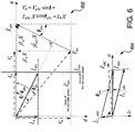
- FIG. 3C is a phasor diagram illustrating vectors for back EMF voltage ⁇ x of a generator, the voltage Vx at the input to a matrix converter, and active ⁇ q and reactive ⁇ d currents from generator 24.
- FIGS. 3A-3C will be discussed together.
- Generator 24 produces back EMF 50 ( eabc ) and has internal inductances LG. In accordance with the notation used with a subscript having multiple letters, a signal or component corresponds to each letter.
- Voltage (vabc) at the output of generator 24 is provided to matrix converter 22.
- the voltage across capacitors C ABC ( v ABC ) is the output voltage of matrix converter 22.
- controller 26 operates to control input voltage ( v abc ) to control current through matrix converter 22. This relationship is seen in FIG 3B .
- ⁇ x designates the voltage vector for the voltage of back EMF 50 ( eabc ).
- V x ⁇ x designates the voltage vector for the input voltage (vabc) to matrix converter 22.
- controller 26 may control the input voltage (vabc). For example, if the input voltage vector V ⁇ is equal to the back EMF vector ⁇ x, no current will be flowing to the input of matrix converter 22.
- FIG. 3C is a phasor diagram illustrating the relationship of the back EMF voltage ( e abc) and the input voltage ( vabc ).
- FIG. 3C includes phasors ⁇ x, V ⁇ x, and ⁇ x.
- ⁇ x is the product of the active current phasor ⁇ q and the reactive current phasor ⁇ d, which are 90° out of phase.
- the active current phasor ⁇ q is in phase with the back EMF voltage ⁇ x.
- the voltage drop across the internal inductance Lg ( j ⁇ L ⁇ x ) balances the input voltage V ⁇ x with the back EMF voltage ⁇ x.
- V ⁇ x can be controlled to control the current ⁇ x to matrix converter 22.
- vabc can be controlled, in part, by controlling switch matrix 22 to connect vABC on the output phases ( A, B, C ) to the input phases ( a, b, c ).
- FIG. 4 is a block diagram illustrating at least a portion of controller 26 for controlling matrix converter 22 using CCM in accordance with certain embodiments of controller 26.
- a generator 416 generates power that is provided to a load 412 via matrix converter 22.
- the load 412 can be unknown and/or variable.
- Control of matrix converter 22 by controller 26 is improved when alignment between vABC and iABC is maintained. With vABC and iABC aligned, voltage vector vabc can have the largest amplitude.
- vabc is proportional to a modulation index of MxC 22, amplitude of vABC, and a phase angle between vABC and iABC, and thus when vectors vABC and iABC are aligned, a vector having a maximized (e.g., largest possible) unity power factor offers the largest control action for controlling generator current.
- the switches (SaA-ScC) of matrix converter 22 are further controlled based on a reference voltage v*ABC provided to the matrix converter 22 as a reference voltage for vABC to create and remove short-circuit paths within matrix converter 22.
- v*ABC can be internally generated, e.g., in an internal microprocessor or provided by an external system that controls MxC 22 as a subsystem.
- the feed forward calculator 419 estimates feed forward current and feed forward load angle, which assist to control a saturation level of PWM controller 409 for operation of the switch matrix of matrix converter 22.
- Saturation of the PWM controller 409 can occur when the output voltage ( v ABC ) has become small compared to the input voltage ( vabc ) due to an inability of the PWM algorithm to control the input voltage ( vabc ) using the small output voltage ( v ABC ) .
- Saturation can be mitigated by controlling matrix converter 22 to generate some reactive current in generator 416 to reduce the demand on the voltage v abc to minimize the possibility of saturation, including to pull the PWM algorithm out of saturation, in other words to avoid saturation during PWM control.
- Generator 416 provides an input voltage v abc to matrix converter 22.
- Generator 416 such as a permanent magnet generator (PMG) is a multiphase generator that includes internal inductances 417 of windings of generator 416.
- Generator 16 is similar in function and structure to generator 24 of FIG. 1 .
- Generator 16 generates back EMF voltage e abc in its windings.
- the output of the matrix converter is provided to a three phase balanced load 412.
- the output voltage v ABC provided to the load 412 can be measured for each phase across capacitors 413, wherein capacitors 413 filter output voltage v ABC .
- Controller 26 includes a PWM controller 409, a complex vector current regulator (CVCR) 404, a magnitude calculator 402, a unity current reference vector generator 411, a feed-forward calculator 419, an Id startup generator 420, a voltage regulator 401, current sensors 422, a 3:2 transform circuit 408, an observer 415, rotators 405 and 407, an Id_trim regulator 414, an active adder 421, a reactive adder 403, a triangle waveform generator 410, and a 2:3 transform circuit 406.
- CVCR complex vector current regulator
- PWM controller 409 implements a matrix converter PWM algorithm such as, for example, space-vector control with triangle comparison, or any other PWM algorithm for matrix converter 22.
- An example PWM controller is described in U.S. Patent Serial No 8,259,474 to Vladimir Blasko , published 2/24/11.
- Feed forward calculator 419 receives output voltage V ABC , back EMF e abc , sensed current i abc , and the matrix converter's 22 D T , and outputs feed forward phase angle and feed forward q and d current components i e* qd_ff .
- the PWM controller 409 receives a triangle waveform from triangle waveform generator 410 and a unity current reference vector 1 I ABC from unity current reference vector generator 411 for implementing space-vector control with triangle comparison.
- the unity current reference vector generator 411 receives the feed forward phase angle ⁇ ABC_ff .
- the unity current reference vector generated by unity current reference vector generator 411 defines the position of current phasor/vector ⁇ ABC that is corrected by the feed forward phase angle ⁇ ABC_ff to adjust a vector V ⁇ ABC representing the output voltage to have a desired position/angle to be aligned with the Q axis (see FIG. 6 ).
- the corrected unity current reference vector ( ⁇ ABC ) that is provided to the matrix converter 22 thus adjusts output voltage position based upon the feed forward phase angle Q ABC_ff .
- the feed forward phase angle ⁇ ABC_ff is used to adjust the vector representing the output voltage V ⁇ ABC to be aligned with the unity voltage reference vector 1 V ABC in the presence of load 412, even when the load 412 is unknown and/or is changing.
- the feed forward q and d current components i qd_ff (also referred to as i q_ff and i d_ff ) are provided, respectively, to active adder 403b and reactive adder 403a, which each apply a function to the respective and feed forward q and d current components i qd_ff .
- output of the respective active and reactive adders 403b and 403a are provided as active and reactive current reference signals i e* q and i e* d to the CVCR 404.
- the active and reactive current reference signals i e* q and i e* d are configured to control power transfer from low voltage (denoted abc ) to high voltage (denoted ABC ), also referred to as low and high sides, respectively.
- Id startup generator 420 operates during startup time when the output voltage v ABC is still forming and has an amplitude significantly below reference value to generate an initial reactive current reference i e* d0 .
- Id startup generator 420 increases or initializes the initial reactive current reference i e* d0 at startup, e.g., as 1 to 1 per unit (pu) value, for a predetermined time interval that is a fraction of a period of the output voltage waveform. Then Id startup generator 420 gradually ramps down the initial reactive current reference i e* d0 , e.g., to zero, after the predetermined time interval. The ramp down can occur, for example, over a 5 to 10 ms time span.
- the initial reactive current reference i e * d0 output by the Id startup generator 420 is combined at reactive adder 403a with feed forward d current component i e d_ff from the feed forward circuit 419 and ⁇ i e d output from Id_trim regulator 414, wherein Id_trim regulator 414 is described further below.
- the output of the reactive adder 403a is the reactive current reference i e * d , which is provided to the CVCR 404.
- Voltage regulator 401 is a proportional integral (PI) output voltage magnitude regulator that uses a PI method to regulate magnitude of the output voltage.
- PI regulators consist of a proportional part and an integral part. The proportional part multiplies error signal with a proportional gain. The integral part integrates an error input signal with an integral gain. Due to integral action, the PI regulator eliminates steady state DC error from the input signal.
- PWM controller 409 receives a triangle waveform from triangle waveform generator 410 to implement a switching matrix S with switching pulses for turning on and off switches in a power stage of matrix converter 22.
- Matrix converter 22 can further receive a unity current reference vector from unity current reference vector generator 411, which uses three cosine functions with unity amplitude 120 degrees apart for defining position angle ⁇ ABC and frequency f 4BC of locally averaged current i ABC at the output of matrix converter 22.
- PWM controller 409 receives a triangle waveform from triangle waveform generator 410 to implement a switching matrix S with switching pulses for turning on and off switches in a power stage of matrix converter 22.
- Matrix converter 22 can further receive a unity current reference vector 1 I ABC from unity current reference vector generator 411, which uses three cosine functions with unity amplitude 120 degrees apart for defining position angle ⁇ ABC and frequency f ABC of locally averaged current i ABC ⁇ at the output of matrix converter 22.
- Locally averaged values of variables like fast changing current or voltages, are averaged values over short sampling interval that can be considered to be constant over short sampling intervals.
- the sampling time can be related to a period of switching of devices in a power circuit of a matrix converter.
- the output voltage ( v ABC ) of matrix converter 22 is sampled by magnitude calculator 402.
- Magnitude calculator 402 is any analog or digital circuit or device capable of outputting a voltage value ( V ) indicative of the magnitude of feedback voltage at capacitors CA, CB, and CC.
- the input voltage ( vabc ) of matrix converter 22 is sampled at the output of generator 416 and provided to observer 415.
- Current ( iabc ) is sampled by current sensors 422 at the output of generator 416 and provided to observer 415, feed forward calculator 419, and 3:2 transform circuit 408.
- Observer 415 is a circuit capable of determining a reference angle ⁇ .
- the observer 415 can include, for example, a position sensor (e.g., a resolver on a shaft of the generator 416) to determine an angular position ( ⁇ abc ) of a rotor of generator 416 based upon the sampled voltage ( vabc ) and current ( iabc ), and thus the position of generated voltage e (back EMF) in the generator.
- observer 415 includes a phase locked loop (PLL) from voltage source e abc if a separate voltage source is used.
- PLL phase locked loop
- 3:2 transform circuit 408 performs an abc -to- dq transformation to convert the three-phase AC signal into two-phase AC signal ( i s q and i s d ) .
- the block 407 performs a rotational transformation on the two-phase AC signal ( i s q and i s d ), creating from them DC-like signals ( i e q and i e d , hereinafter referred to as "static DC signals").
- Controller 26 receives a reference voltage vector v * ABC having magnitude
- a BC ) is provided to voltage regulator 401.
- voltage regulator 401 uses the reference input ( v* ABC ) and the measured voltage magnitude (
- the regulated active current signal i e* Q output by voltage regulator 401 is combined at active adder 403b with feed forward q current component i q_ff to form active reference current signal i e* q , which is provided to the active current regulator in CVCR 404, which includes active ( q ) and reactive ( d ) current regulators.
- the output of CVCR 404, components v d and v q are introduced into PWM controller 409 through rotator 405, and then through 2:3 transform circuit 406, as a three phase signal voltage reference signal v* abc
- the three phase voltage reference signal v* abc is after zero sequence injection, compared with triangle waveform signal vt and should not exceed its amplitude in order to avoid PWM saturation.
- voltage reference signal v* abc is transformed from v e * qd , the v e * qd , signal is input to Id_trim regulator 414, wherein the output signal of the Id_trim regulator 414 s indicative of saturation of the PWM algorithm.
- Id_trim regulator 414 is configured to output a control signal ( ⁇ id* ) indicative of a desired change in reactive current, wherein ( ⁇ id* ) is used to avoid saturation of the PWM controller 409 by reducing demand on voltage v abc which is proportional to voltage reference signal v* abc and consequently to v e * qd
- Reactive adder 403a is used to adjust the reactive current control signal ( id e * ) based on the desired change in reactive current ( ⁇ id* ) from Id_trim regulator 414 and feed forward reactive current i e* d_ff .
- the output of reactive adder 403a is provided to CVCR 404.
- Active adder 403b is used to adjust the regulated active current signal ( i e* Q ) output by voltage regulator 401 based on feed forward active current i e* q_ff .
- the output of active adder 403b is also provided to CVCR 404.
- CVCR 404 includes regulators for regulating active current ( i e q ) and reactive current ( i e d ) , implemented in a synchronous - rotating reference frame received output from rotator 407 using the respective active and reactive current control signals output by active adder 403b and reactive adder 403a.
- currents i e q and i e d can be regulated by separate synchronous reference frame q and d regulators.
- CVCR 404 can be viewed as an improved version of q and d separate regulators with inherent cross coupling as known to these familiar with theory of operation of CVCR.
- CVCR regulator 404 generates a voltage indicative of a difference between the regulated active and reactive current feedback ( i e q , i e d , respectively) and provides the voltage v e* qd to rotator 405.
- Rotator 405 receives the two DC like voltages, components v d and v q , from CVCR 404. Rotator 405 also receives a control angular position ( ⁇ abc ) . Controller 26 uses the control angular position ( ⁇ abc ) to control the frequency of the voltage ( v abc ) . Rotator 405 converts the two DC like voltages, components v d and v q , and provides v d and v q to 2:3 transform circuit 406.
- 2:3 transform circuit 406 performs a d s q s -to-abc transformation on the two ac voltages in d s q s stationary reference frame to generate three-phase signals v abc for PWM controller 409.
- PWM controller 409 then uses the three-phase signals v abc to control matrix converter 22.
- the superscript s represents a stationary reference frame, wherein signals in a stationary frame are AC sinusoidal signals and signals in a rotating frame are steady DC-like signals.
- Matrix converter system 10 has several advantages over a matrix converter that operates in the VCM mode. By controlling matrix converter system 10 using CCM, the input LC circuit may be removed, and output voltage can be filtered by only additional three capacitors, one per phase. This reduces the size and weight of the matrix converter system. Matrix converter system 10 is also able to operate in a boost mode, allowing voltage operation at the output above 86.6% of the input voltage (the generator's 416 back EMF) which has been a major drawback in previous matrix converter system design.
- CVCR 404 regulates i e q and i e d current components to follow current references i e * q and i e * d .
- Output of CVCR 404 is a voltage vector v e * qd , which after transformation into stationary reference frame and into abc coordinates by 2:3 transform circuit 406, becomes v* abc v* abc is a modulation input into PWM controller 409, which creates v abc on a low-voltage side from available voltage on high-voltage side, namely v ABC COS ⁇ ABC .
- voltage v abc is proportional to the modulation voltage v* abc and v ABC cos ⁇ ABC .
- the load power factor has an impact on available voltage and control of source current on the low-voltage side.
- Feed forward values of I q and I d current are calculated based on power demand at output of matrix controller 22 and also based on a need for reactive I d current component to provide an amount of voltage to still maintain PWM controller 409 below saturation level, having modulation index m ⁇ 1.
- Modulation index is the ratio between amplitude of voltage reference signal v* abc and peak value of triangle waveform from block 410.
- FIG. 5 shows an equivalent circuit of the matrix converter 22 with a positive direction of power flow defined to be from low-voltage abc side 502 to high-voltage ABC side 504.
- FIG. 6 shows a phasor diagram of the low-voltage side in plot 602 and the high-voltage side in plot 604 of the matrix converter 22. Phasors are defined with their amplitudes and phase angle in a complex plane captured at a specific moment in the time. Phasor notation is indicated by a dot above a capital letter. Magnitude of the phasor is indicated by usage of the capital letter without the dot.
- Equations (1) - (6) it was adopted that amplitude of each phasor was equal to the peak value of sinusoidal voltage from the voltage source, e.g., generator 416.
- Typical convention for phasors uses the root mean square (RMS) value of sinusoidal waveforms, which is 2 times smaller than peak value.
- RMS root mean square
- Equation (9) describes example calculations for determining the current I abc on the low side 502:
- FIG. 7 provides a flow diagram 700 that shows an example method of performance of generating feed forward references for reactive and active current signals i d and i q currents is shown and deriving angle ⁇ abc_ff between output voltage and current that is used adjust the position of output current i ABC to cause voltage vector v ABC to be positioned at a desired location.
- Equation (1) is performed to generate ⁇ abc which is provided to function 1/X at block 704.
- the output of block 704, I SC abc , where the superscript SC indicates "short circuit", is provided to block 706.
- a function e.g., multiplier function
- i abc and D T ⁇ S T are provided to operation 710.
- Operation 710 further receives feedback signal V ABC .
- Equations (2) - (6) are performed on the inputs.
- the outputs of Equations (2) - (6) are provided to operation 706 and operation 724.
- equation 14 is performed and sine and cosine values of load angle ⁇ are input to operations 714 and 716, respectively.
- the output of operations 716 and 702 are provided to operation 718 to operation 714 which performs a function on these two output values.
- the output of operations 714 and 720 are provided to operations 720.
- a function 1/X is applied and the output is provided to operation 722.
- Operation 722, namely 1/ (1+ skT s ) includes application of a filter that causes a delay in the generation of the feed forward active and reactive currents i qd_ff .
- a function is applied to ⁇ ABC received from operation 710 and ⁇ ABC _ ff is output.
- the function applied at operation 724 includes application of a filter that causes a delay in the generation of the feed forward output phase angle ⁇ ABC_ff .
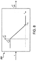
- FIG. 8 shows an operation 800 performed by Id startup generator 420 in which, based on the passage of time, for a predetermined first time interval, current reference i e* d0 i s set to a selected value, after which the value of current reference i e* d0 is ramped down to about zero over a second predetermined time interval ending at time t 0 .
- FIG. 9 a block diagram showing application of the feed forward phase angle ⁇ ABC_ff is shown.
- Plots 902 and 904 show how the position of current phasor/vector ⁇ ABC is adjusted by estimated angle ⁇ ABC_ff to keep the voltage phasor/vector at a selected position to be aligned with the Q axis.
- a voltage reference generator 1024 and a generator 416' configured to have controllable back EMF are provided. Control of the back EMF of generator 416' can be performed using an induction motor or generator. For example, the back EMF can be controlled through rotor flux vector control.
- the voltage reference generator 1024 generates a reference signal
- a scaling circuit 1026 receives an input signal from the output from reactive adder 403, which is a function of the feed forward reactive current i d_ff , current reference i e* d0 , and desired change in reactive current ⁇ id * from Id_trim regulator 414.
- a scaling function is applied to relate the input signal to a desired voltage change, namely a target back EMF value
- a regulator 1028 performs a regulator function on the output of the scaling circuit 1026 and outputs the reference signal
- functions as a control signal to control the source voltage from the generator 416 and/or the back EMF from the generator 416.
- CVCR 404 When generator voltage is controlled by the controller 26, CVCR 404 does not receive the output from reactive adder 403, and rather receives id e* , which can be kept close to zero or equal to zero. In this way, total current load of the source/controllable generator is kept to a minimum with minimal losses occurring in the generator 416 and matrix converter 22.
- This change in input to CVCR 404 relative to the embodiment shown in FIG. 4 is due to using regulation of the back EMF of generator 416' to keep PWM out of saturation, such application of feed forward reactive current i d_ff and/or desired change in reactive current ⁇ id* from Id_trim regulator 414 to CVCR 404 is not necessary for controlling saturation of PWM controller 409.
- FIG. 11 a block diagram of an example computing system 1100 is shown, which provides an example configuration of the controller 26 or one or more portions of the controller 26.
- Computing system 1100 is only one example of a suitable system and is not intended to suggest any limitation as to the scope of use or functionality of embodiments of the disclosure described herein.
- Computing system 1100 can be implemented using hardware, software, and/or firmware. Regardless, computing system 1100 is capable of being implemented and/or performing functionality as set forth in the disclosure.
- Computing system 1100 is shown in the form of a general-purpose computing device.
- Computing system 1100 includes a processing device 1102, memory 1104, an input/output (I/O) interface (I/F) 1106 that can communicate with an internal component 1110, and optionally an external component 1108.
- I/O input/output
- I/F input/output interface
- the processing device 1102 can include, for example, a programmable logic device (PLOD), microprocessor, digital signal processor (DSP), a microcontroller, a field programmable gate array (FPGA), an application specific integrated circuit (ASCI), and/or other discrete or integrated logic circuitry having similar processing capabilities.
- POD programmable logic device
- DSP digital signal processor
- FPGA field programmable gate array
- ASCI application specific integrated circuit
- the processing device 1102 and the memory 1104 can be included in components provided in the FPGA, ASCI, microcontroller, or microprocessor, for example.
- Memory 1104 can include, for example, volatile and non-volatile memory for storing data temporarily or long term, and for storing programmable instructions executable by the processing device 1102.
- I/O I/F 1106 can include an interface and/or conductors to couple to the one or more internal components 1108 and/or external components 1110.
- These computer program instructions may also be stored in a computer readable medium that can direct a computer, other programmable data processing apparatus, or other devices to function in a particular manner, such that the instructions stored in the computer readable medium produce an article of manufacture including instructions which implement the function/act specified in the flow diagram and/or block diagram block or blocks.
- the computer program instructions may also be loaded onto a computer, other programmable data processing apparatus, or other devices to cause a series of operational operations to be performed on the computer, other programmable apparatus or other devices to produce a computer implemented process such that the instructions which execute on the computer or other programmable apparatus provide processes for implementing the functions/acts specified in the block diagram block or blocks.
- Embodiments of the controller 26 may be implemented or executed by one or more computer systems, such as a microprocessor. Each computer system 1100 can implement controller 26, or multiple instances thereof. In various embodiments, computer system 1100 may include one or more of a microprocessor, an FPGA, application specific integrated circuit (ASCI), microcontroller. The computer system 1100 can be provided as an embedded device. All or portions of the computer system 1100 can be provided externally, such by way of a mobile computing device, a smart phone, a desktop computer, a laptop, or the like.
- a mobile computing device such as a smart phone, a desktop computer, a laptop, or the like.
- Computer system 1100 is only one example of a suitable system and is not intended to suggest any limitation as to the scope of use or functionality of embodiments of the disclosure described herein. Regardless, computer system 1100 is capable of being implemented and/or performing any of the functionality set forth hereinabove.
- Computer system 1100 may be described in the general context of computer system-executable instructions, such as program modules, being executed by a computer system.
- program modules may include routines, programs, objects, components, logic, data structures, and so on that perform particular tasks or implement particular abstract data types.
Landscapes
- Engineering & Computer Science (AREA)
- Power Engineering (AREA)
- Ac-Ac Conversion (AREA)
- Dc-Dc Converters (AREA)
Abstract
Description
- The present disclosure relates to a matrix converter, and more particularly, to a matrix converter operating in current control mode using feed forward signals.
- Matrix converters are generally used as alternating current (AC)-to-AC converters that receive a multiphase input and produce a multiphase output. Traditional matrix converters operate in voltage control mode (VCM) such that the output voltage is controlled directly based upon the input voltage. In systems that utilize VCM, input inductor-capacitor (LC) circuits are implemented at the input of the matrix converter. The input LC circuit generally includes capacitors connected between each phase of the input. These capacitors create low impedance paths between phases and thus, the matrix converter cannot be controlled to provide short circuits between input phase lines without risking damage to the switching elements. Since the matrix converter cannot create output voltages higher than the line-to-line input voltages, the matrix converter's ability to provide output voltage without distortion is limited. Specifically, the matrix converter is not able to provide an output voltage that is greater than 86.6% of the input voltage without distortion.
- While conventional methods and systems have generally been considered satisfactory for their intended purpose, there is still a need in the art for a matrix converter that can operate safely regardless of the output voltage level.
- The purpose and advantages of the below described illustrated embodiments will be set forth in and apparent from the description that follows. Additional advantages of the illustrated embodiments will be realized and attained by the devices, systems and methods particularly pointed out in the written description and claims hereof, as well as from the appended drawings.
- To achieve these and other advantages and in accordance with the purpose of the illustrated embodiments, in one aspect, disclosed is a matrix converter system having a current control mode operation. The system includes a matrix converter having a switching matrix. The matrix converter is coupled at its low-voltage side to a generator and at its output load side to a load. A controller having a pulse width modulation (PWM) controller is configured to control the matrix converter via its switching matrix to increase energy within internal inductances of the generator when the switching matrix causes a short circuit. A feed forward calculator is configured to calculate a feed forward output phase angle, the feed forward output phase angle being an estimation of an angle between current and voltage output by the matrix converter. The angular position of the voltage output by the matrix converter is adjusted as a function of the feed forward output phase angle output voltage with desired phase angle or position.
- In embodiments, the feed forward calculator can be further configured to calculate feed forward values of active and reactive currents with respect to back electromotive frequency (EMF) of the generator. The feed forward values of the active and reactive current can be used to adjust currents that affect the controller to minimize the possibility of saturation of the PWM controller.
- In embodiments, calculation of the feed forward active and reactive currents at the position with respect to the back EMF of the generator can be a function of magnitude and phase angle position of an EMF vector that represents the back EMF of the generator.
- In embodiments, the feed forward calculator is further configured to apply filter to generate the feed forward active and reactive currents.
- In embodiments, the system can include a startup generator configured to provide an amount of startup reactive current during a startup phase of the generator. The control circuit can be configured to receive the startup reactive current and provide an amount of voltage as a function of the startup reactive current to the controller during the startup phase, wherein the amount of voltage can be sufficient to avoid saturation of the PWM controller.
- In embodiments, the startup reactive current can be maintained for a first interval of time and can be ramped down to about zero over a second interval of time interval.
- In embodiments, the system further can include a plurality of output capacitors connected to phases of the current output by the matrix converter. The controller can be further configured to control the matrix converter to increase the energy in the internal inductance of the generator, wherein the increase in energy can be sufficient to cause current from the generator to charge the output capacitors.
- In embodiments, the feed forward output phase angle is provided to a unity current reference vector function that implements space-vector control to generate a unity reference current vector having a position defined by the feed forward output phase angle to adjust the angular position of the voltage output by the matrix converter.
- In embodiments, the feed forward calculator is further configured to apply a filter to generate the feed forward output phase angle.
- In another aspect, a method of controlling operation of a matrix converter operating in a current control mode operation is provided. The matrix converter is coupled at its input low-voltage side to a generator. At its output load side, the matrix converter is connected to a load. The method includes controlling pulse width modulation (PWM) to control the matrix converter to increase energy within internal inductances of the generator when a short circuit occurs. The method further includes calculating a feed forward output phase angle. The feed forward output phase angle is an estimation of an angle between an output current vector and an output voltage vector that represent feedback signals of current and voltage output by the matrix converter. The method further includes adjusting an angular position of the voltage output by the matrix converter as a function of the feed forward output phase angle. The adjusting of the angular position of the voltage output is performed in order to align an output voltage vector that represents the voltage output with a selected position.
- In embodiments, the method can further include calculating feed forward values of active current and the reactive current with respect to back EMF of the generator. The feed forward values of the active and reactive current from the generator can be used to adjust currents that affect control of the matrix converter to minimize the possibility of saturation during PWM control.
- In embodiments, calculation of at least one of the feed forward values of the active and reactive current can be a function of back EMF of the generator.
- In embodiments, controlling the matrix converter to increase energy within the internal inductances of the generator when a short circuit occurs, wherein the increase in energy can be sufficient to cause current from the generator to charge output capacitors connected to the current output by the matrix converter.
- In embodiments, the method further can include providing during a startup phase of the generator an amount of startup reactive current, receiving the startup reactive current, and providing an amount of voltage as a function of the startup reactive current for controlling the matrix converter during the startup phase. The amount of voltage can be sufficient to avoid saturation during PWM control.
- In embodiments, the method can further include maintaining the startup reactive current for a first interval of time and ramping down the startup reactive current to about zero over a second interval of time interval.
- In accordance with still another aspect of the disclosure, a matrix converter system having a current control mode operation is provided. The system includes a matrix converter having a switching matrix, the matrix converter being coupled at its low-voltage side to a generator and coupled at its output load side to a load. A controller having a pulse width modulation (PWM) controller is configured to control matrix converter via its switching matrix to increase energy within internal inductances of the generator when a short circuit occurs in the switching matrix. A feed forward calculator is configured to calculate feed forward values of active and reactive current. The feed forward values of the active and reactive current are calculated based on power demand at the output of the matrix converter. The feed forward values of the active and reactive current are used to adjust currents that affect input to the controller to minimize the possibility of saturation of the PWM controller.
- In embodiments, the multiphase voltage source has controllable back EMF. The system can further include a voltage reference generator configured to receive an input signal that is a function of the feed forward values and a magnitude of reactive current and configured to adjust the back EMF of the generator based at least in part on the input signal.
- In embodiments, the voltage reference generator can be configured to receive a target back EMF value, determine a voltage change based on a difference between the input signal and the target back EMF value, and can be further configured to output a voltage reference to the generator. The voltage reference can be based on the voltage change.
- In embodiments, determining the voltage change can include applying a current scaling function to the input signal.
- In embodiments, calculation of the feed forward values of the active and reactive current is a function of back EMF of the generator
- In embodiments, the system can further include a plurality of output capacitors connected to phases of the multiphase output, wherein the controller can be further configured to control the matrix converter to generate the energy in the internal inductance of the generator, wherein the increase in energy can be sufficient to cause current from the generator to charge the output capacitors.
- In embodiments, the system can further include a startup generator configured to provide an amount of startup reactive current during a startup phase of the generator. The control circuit can be configured to receive the startup reactive current and provide an amount of voltage as a function of the startup reactive current to the controller during the startup phase, the amount of voltage being sufficient to avoid saturation of the PWM controller.
- In embodiments, the startup reactive current can be maintained for a first interval of time and can be ramped down to about zero over a second interval of time interval.
- These and other features of the systems and methods of the subject disclosure will become more readily apparent to those skilled in the art from the following detailed description of the embodiments taken in conjunction with the drawings.
- So that those skilled in the art to which the subject disclosure appertains will readily understand how to make and use the devices and methods of the subject disclosure without undue experimentation, embodiments thereof will be described in detail herein below, by way of example only and with reference to certain figures, wherein:
-
FIG. 1 is a circuit diagram illustrating an example matrix converter system that utilizes a current control mode in accordance with embodiments of the disclosure; -
FIGS. 2A-2C are circuit diagrams illustrating an example switch matrix, an example bidirectional switch, and an example damping circuit, respectively, for the matrix converter system ofFIG. 1 ; -
FIG. 3A is a line diagram illustrating a back electromotive force (EMF) of an example generator connected to an input of a matrix converter in accordance with embodiments of the disclosure; -
FIG. 3B is a line diagram illustrating a balance between the back EMF of a generator and an input voltage of an example matrix converter system in accordance with embodiments of the disclosure; -
FIG. 3C is a phasor diagram illustrating vectors for back EMF voltage of an example generator, the voltage at the input to a matrix converter, and active and reactive currents from the generator in accordance with embodiments of the disclosure; -
FIG. 4 is a block diagram illustrating an example controller for controlling a matrix converter using a current control mode in accordance with embodiments of the disclosure; -
FIG. 5 is a diagram of an equivalent circuit of an example matrix converter in accordance with embodiments of the disclosure; -
FIG. 6 is a phasor diagram of low and high-voltage sides of the matrix converter ofFIG. 5 ; -
FIG. 7 is a flow diagram of an example method performed by an example controller of a matrix converter ofFIG. 4 ; -
FIG. 8 is a graph of an example plot of an input reactive current provided by an ID startup generator ofFIG. 4 ; -
FIG. 9 are phasor diagrams of showing correction of a current phasor/vector in accordance with embodiments of the disclosure; -
FIG. 10 is a block diagram illustrating an example voltage reference generator and an example controller for controlling a matrix converter using a current control mode in accordance with embodiments of the disclosure and -
FIG. 11 is a block diagram of an exemplary computer system configured to implement components of a controller of the matrix converter system ofFIG. 1 . - A matrix converter system is disclosed herein that operates from a controllable voltage source in a current control mode (CCM). The matrix converter system includes a matrix converter and a controller configured to control the matrix converter. The controller is configured to calculate a feed forward output phase angle, the feed forward output phase angle being an estimation of an angle between current and voltage output by the matrix converter. The angular position of the voltage output by the matrix converter is adjusted as a function of the feed forward output phase angle output voltage with desired phase angle or position.
- In embodiments, the feed forward calculator can be further configured to calculate feed forward values of active and reactive currents with respect to back electromotive frequency (EMF) of the generator. The feed forward values of the active and reactive current can be used to adjust currents that affect the controller to minimize the possibility of saturation of the PWM controller.
- In embodiments, the feed forward values of the active and reactive current can be calculated based on power demand at the output of the matrix converter.
- The controller can include a startup generator configured to provide an amount of startup reactive current during a startup phase of the generator. The control circuit can be configured to receive the startup reactive current and provide an amount of voltage as a function of the startup reactive current to the controller during the startup phase, the amount of voltage being sufficient to avoid saturation of the PWM controller.
- A generator of the matrix converter system can be configured to have controllable back EMF. The controller can include a voltage reference generator configured to receive an input signal that is a function of the feed forward values and a magnitude of reactive current. The voltage reference generator can further be configured to adjust the back EMF of the generator based at least in part on the input signal. In embodiments, the voltage reference generator can be configured to receive a target back EMF value, determines a voltage change based on a difference between the input signal and the target back EMF value, and output a voltage reference to the generator, wherein the voltage reference is based on the voltage change.
- The matrix converter does not include an inductor-capacitor (LC) input filter and thus, there are no line-to-line capacitors on the input side of the matrix converter. The input of the matrix converter is connected to receive power from a multiphase generator. The generator includes internal inductances on each phase. Capacitors are connected between each output phase of the matrix converter and ground.
- The matrix converter system is capable of operating in a boost mode. When the voltage on the output capacitors is relatively small, switches of a switching matrix of the matrix converter may be operated to short phase lines to increase energy within the internal inductances of the generator when short-circuited. This is possible due to the absence of the LC circuit at the input, which removes the low impedance line-to-line capacitors. Upon generation of energy within the internal inductances of the generator, the switches of the matrix converter may then be controlled to provide current to charge the output capacitors using the generated energy stored in the inductances of the generator. This way, the output capacitors may be charged to a voltage greater than that of the input voltage. Once the voltage on the output capacitors is sufficient, the matrix converter may be controlled normally to control the output to a load.
- Reference will now be made to the drawings wherein like reference numerals identify similar structural features or aspects of the subject disclosure. For purposes of explanation and illustration, and not limitation, a block diagram of an exemplary embodiment of a matrix converter system in accordance with the disclosure is shown in
FIG. 1 and is designated generally byreference character 10. Methods associated with operations of thematrix converter system 10 in accordance with the disclosure, or aspects thereof, are provided inFIGS. 2 -11 as will be described. The systems and methods described herein can be used to provide improved control of a saturation level of pulse width modulation (PWM) for operation of a switch matrix in a matrix converter. -
FIG. 1 is a circuit diagram illustratingmatrix converter system 10 capable of operation in a current control mode (CCM).Matrix converter system 10 includesmatrix converter 22 connected to receive input power from three-phase generator 24 on input phases (a, b, c).Matrix converter 22 include switches SaA, SaB, SaC, SbA, SbB, SbC, ScA, ScB, and ScC (hereinafter "SaA-ScC") that each receive control signals fromcontroller 26. The switches ofmatrix converter 22 are controlled to convert input power on input phases (a, b, c) to output power on the output phases (A, B, C). Capacitors CA, CB, and CC are connected to the three respective output phases (A, B, C) ofmatrix converter 22. Damp circuit 28 (illustrated in further detail inFIG. 2C ) is connected to the three phase inputs ofmatrix converter 22.Generator 24 is connected directly tomatrix converter 22 through grounded sheath 30. An electromagnetic interference (EMI)filter 32 can be connected to the output ofmatrix converter 22 to provide further filtering forsystem 10. While illustrated as three input phases (a, b, c) and three output phases (A, B, C), any number of input phases and any number of output phases may be connected throughmatrix converter 22. -
Matrix converter system 10 does not include inductors or capacitors at the input ofmatrix converter 22. By eliminating the capacitors at the input ofmatrix converter 22, the low impedance paths between phases (a, b, c) on the input side ofmatrix converter 22 are eliminated. The internal inductances ofgenerator 24 create high impedances and thus, switches SaA-ScC may be controlled such that phase-to-phase short circuits are created without the risk of generating damaging overcurrents. This allowssystem 10 to utilize the internal inductances ofgenerator 24 to generate reactive currents, which can be utilized to charge output capacitors CA, CB, and CC. This allowsmatrix converter system 10 to operate in a boost mode, generating currents to charge capacitors CA, CB, and CC even when the voltage on output phases (A, B, C) is relatively small. Thus,system 10 is able to overcome the 86.6% input-to-output voltage limit of matrix converter systems that operate in VCM mode only. -
Controller 26controls matrix converter 22 using a PWM control scheme.Controller 26 can be implemented using hardware, firmware, software, or a combination thereof.Controller 26 observes the current on input phases (a, b, c) and the voltage on output phases (A, B, C) to controlmatrix converter 22.Controller 26 may select a desired output frequency that is independent of the input frequency. For example, the output may be a three-phase AC output at a frequency greater than, or less than, that ofgenerator 24.Generator 24 may also be a variable frequency generator, such that the frequency is at times greater than the output frequency, and at times less than the output frequency. The output frequency may also be selected to be zero, allowing formatrix converter 22 to generate a DC output from the AC input. - When the system is starting up, or if the voltage on the output phases (A, B, C) becomes relatively small,
controller 26 may controlmatrix converter 22 in a boost mode in order to boost the voltage on output phases (A, B, C). To do this,controller 26 may control select switches SaA-ScC) to provide one or more short-circuit paths between input phases (a, b, c). These short-circuit paths rely on the high impedances created by the internal inductance ofgenerator 24. During the short-circuit condition, energy is generated within the internal inductances ofgenerator 24. After a selected time, switches (SaA-ScC) are controlled to remove the short circuit, and utilize the energy stored in the internal inductances ofgenerator 24 to direct current to charge capacitors CA, CB, and CC, which allowssystem 10 to create output voltages greater than the input voltages. - In contrast to
system 10 that operates in the CCM mode, certain matrix converter systems that operate in a voltage control mode (VCM) are configured to provide an AC-AC voltage conversion that provides three-phase smooth voltage on the output phases. An input inductor-capacitor (LC) circuit is implemented at an input of the system's matrix converter. The input LC circuit generally includes capacitors connected between each phase of the input However, in certain applications, such as motor control applications, a motor can tolerate discontinuous voltages and therefore, motor windings can be directly connected to the output of such a matrix converter. - When operating in VCM, output voltage may be controlled and limited by the available input voltage. Due to the capacitors connected between the input and output phases, there exists a low impedance path between each input phase lines. Because of this, switches of this matrix converter cannot be controlled to provide a short circuit between any of the input phase lines. If a short circuit were created, the low impedance path created by these capacitors would create a large current, risking damage to the switches. Without any energy storage devices present in such a matrix converter to boost voltage during conversion, analysis has shown that operation of the matrix converter in VCM can only achieve, at best, 86.6% of the input voltage at the output.
-
FIGS. 2A-2B are circuit diagrams illustrating a switch matrix formatrix converter 22, abidirectional switch 40, anddamp circuit 28, respectively.FIG. 2A illustrates an embodiment ofmatrix converter 22. As illustrated inFIG. 2A ,matrix converter 22 may have any number (n) of input phases, and any number (m) of output phases. In the embodiment illustrated inFIG. 1 , matrix converter has three input phases (n=3) and three output phases (m=3). As illustrated inFIG. 2A ,matrix converter system 10 may be configured to generate any number of output phases from any number of input phases. - The
matrix converter 22 is described by equations (A) and (B):

matrix converter 22. When a high sampling rate and short sampling time Ts is used, it can be assumed that input and output voltages and currents have negligible small changes and can be considered constant, such that switching matrix S can be replaced with duty cycle matrix D, as shown in Equations (A) and (B), wherev abc andi abc are locally averaged values of vabc and iabc . -
FIG. 2B illustratesbidirectional switch 40. In prior art systems, matrix converters included bidirectional switches implemented using insulated gate bipolar transistors (IGBTs), for example. The use of IGBTs required the use of diodes to properly achieve bidirectional power flow.Bidirectional switch 40, in contrast, uses metal-oxide-semiconductor field-effect transistors (MOSFETs) 42 and 44, which may be silicon carbide (SiC) MOSFETs, for example. MOSFETs are channel devices that do not require the use of external diodes, as the internal channels of the MOSFET accomplish this task. Thus,bidirectional switch 40 may be accomplished by connecting the drains ofMOSFETs -
FIG. 2C illustrates an embodiment ofdamp circuit 28. As seen inFIG. 1 , and in contrast to a matrix converter system that operates in VCM mode,damp circuit 28 is only connected to the input side ofmatrix converter 22. This is due to the absence of an LC circuit, in particular inductors of the LC circuit, provided at the input side of thematrix converter 22.Damp circuit 28 is configured such that if there is a disruption of current flow, the energy stored in the internal inductances ofgenerator 24 has a path.Damp circuit 28 includes diodes D1-D7, capacitor CD, resistor RD, and switch SD. Diodes D1-D6 form a rectifier circuit. The energy stored in the internal inductances ofgenerator 24 upon shutdown ofmatrix converter 22, for example, flows through the rectifier circuit and charges capacitor CD. Switch SD may then be controlled to discharge capacitor CD through resistor RD. -
FIGS. 3A-3C are diagrams illustrating voltage and current relationships withinsystem 10.FIG. 3A is a line diagram illustrating aback EMF 50 ofgenerator 24 connected to the input ofmatrix converter 22.FIG. 3B is a line diagram illustrating a balance between the back EMF voltage Ex ofgenerator 24 and input voltage Vx tomatrix converter 22.FIG. 3C is a phasor diagram illustrating vectors for back EMF voltage Ėx of a generator, the voltage Vx at the input to a matrix converter, and active İq and reactive İd currents fromgenerator 24.FIGS. 3A-3C will be discussed together. -
Generator 24 produces back EMF 50 (eabc) and has internal inductances LG. In accordance with the notation used with a subscript having multiple letters, a signal or component corresponds to each letter. Voltage (vabc) at the output ofgenerator 24 is provided tomatrix converter 22. The voltage across capacitors CABC (vABC ) is the output voltage ofmatrix converter 22. For CCM,controller 26 operates to control input voltage (vabc ) to control current throughmatrix converter 22. This relationship is seen inFIG 3B . Ėx designates the voltage vector for the voltage of back EMF 50 (eabc). VxĖx designates the voltage vector for the input voltage (vabc) tomatrix converter 22. İx designates the current vector for current flowing through internal inductances Lg. Thus, to control current flow in input phases (a, b, c),controller 26 may control the input voltage (vabc). For example, if the input voltage vector Vẋ is equal to the back EMF vector Ėx, no current will be flowing to the input ofmatrix converter 22. -
FIG. 3C is a phasor diagram illustrating the relationship of the back EMF voltage (eabc) and the input voltage (vabc).FIG. 3C includes phasors Ėx, V̇x, and İx. İx is the product of the active current phasor İq and the reactive current phasor İd, which are 90° out of phase. The active current phasor İq is in phase with the back EMF voltage Ėx. The voltage drop across the internal inductance Lg (jωLİx) balances the input voltage V̇x with the back EMF voltage Ėx. The voltage drop across inductor LG (jωLİx) is the result of the voltage drop due to the active current (jωLİq) and due to the reactive current (jωLİd). Thus, as can be seen inFIGS. 3B and3C , V̇x can be controlled to control the current İx tomatrix converter 22. As seen inFIG. 3A , vabc can be controlled, in part, by controllingswitch matrix 22 to connect vABC on the output phases (A, B, C) to the input phases (a, b, c). -
FIG. 4 is a block diagram illustrating at least a portion ofcontroller 26 for controllingmatrix converter 22 using CCM in accordance with certain embodiments ofcontroller 26. Agenerator 416 generates power that is provided to aload 412 viamatrix converter 22. Theload 412 can be unknown and/or variable. Control ofmatrix converter 22 bycontroller 26 is improved when alignment between vABC and iABC is maintained. With vABC and iABC aligned, voltage vector vabc can have the largest amplitude. Those skilled in the art will recognize that vabc is proportional to a modulation index ofMxC 22, amplitude of vABC, and a phase angle between vABC and iABC, and thus when vectors vABC and iABC are aligned, a vector having a maximized (e.g., largest possible) unity power factor offers the largest control action for controlling generator current. The switches (SaA-ScC) ofmatrix converter 22 are further controlled based on a reference voltage v*ABC provided to thematrix converter 22 as a reference voltage for vABC to create and remove short-circuit paths withinmatrix converter 22. v*ABC can be internally generated, e.g., in an internal microprocessor or provided by an external system that controlsMxC 22 as a subsystem. - The feed
forward calculator 419 estimates feed forward current and feed forward load angle, which assist to control a saturation level ofPWM controller 409 for operation of the switch matrix ofmatrix converter 22. Saturation of thePWM controller 409 can occur when the output voltage (vABC ) has become small compared to the input voltage (vabc) due to an inability of the PWM algorithm to control the input voltage (vabc) using the small output voltage (vABC ). Saturation can be mitigated by controllingmatrix converter 22 to generate some reactive current ingenerator 416 to reduce the demand on the voltage vabc to minimize the possibility of saturation, including to pull the PWM algorithm out of saturation, in other words to avoid saturation during PWM control. -
Generator 416 provides an input voltage vabc tomatrix converter 22.Generator 416, such as a permanent magnet generator (PMG), is a multiphase generator that includesinternal inductances 417 of windings ofgenerator 416. Generator 16 is similar in function and structure togenerator 24 ofFIG. 1 . Generator 16 generates back EMF voltage eabc in its windings. The output of the matrix converter is provided to a three phasebalanced load 412. The output voltage vABC provided to theload 412 can be measured for each phase acrosscapacitors 413, whereincapacitors 413 filter output voltage vABC. -
Controller 26 includes aPWM controller 409, a complex vector current regulator (CVCR) 404, amagnitude calculator 402, a unity currentreference vector generator 411, a feed-forward calculator 419, anId startup generator 420, avoltage regulator 401, current sensors 422, a 3:2transform circuit 408, anobserver 415,rotators Id_trim regulator 414, an active adder 421, a reactive adder 403, atriangle waveform generator 410, and a 2:3transform circuit 406. -
PWM controller 409 outputs control signals generated using pulse modulation to control switches SaA-ScC (for Sij, i=a-c and j-A-C, as shown inFIGS. 2-3C ) ofmatrix converter 22.PWM controller 409 implements a matrix converter PWM algorithm such as, for example, space-vector control with triangle comparison, or any other PWM algorithm formatrix converter 22. An example PWM controller is described inU.S. Patent Serial No 8,259,474 to Vladimir Blasko , published 2/24/11. - Feed
forward calculator 419 receives output voltage VABC, back EMF eabc, sensed current iabc, and the matrix converter's 22 DT , and outputs feed forward phase angle and feed forward q and d current components ie* qd_ff. - In the example shown, the
PWM controller 409 receives a triangle waveform fromtriangle waveform generator 410 and a unitycurrent reference vector 1I ABC from unity currentreference vector generator 411 for implementing space-vector control with triangle comparison. The unity currentreference vector generator 411 receives the feed forward phase angle θABC_ff. The unity current reference vector generated by unity currentreference vector generator 411 defines the position of current phasor/vector İABC that is corrected by the feed forward phase angle θABC_ff to adjust a vector V̇ABC representing the output voltage to have a desired position/angle to be aligned with the Q axis (seeFIG. 6 ). The corrected unity current reference vector (İABC ) that is provided to thematrix converter 22 thus adjusts output voltage position based upon the feed forward phase angle QABC_ff. The feed forward phase angle θABC_ff is used to adjust the vector representing the output voltage V̇ABC to be aligned with the unityvoltage reference vector 1V ABC in the presence ofload 412, even when theload 412 is unknown and/or is changing. - The feed forward q and d current components iqd_ff (also referred to as iq_ff and id_ff ) are provided, respectively, to
active adder 403b andreactive adder 403a, which each apply a function to the respective and feed forward q and d current components iqd_ff. As described below, output of the respective active andreactive adders CVCR 404. The active and reactive current reference signals ie* q and ie* d are configured to control power transfer from low voltage (denoted abc) to high voltage (denoted ABC), also referred to as low and high sides, respectively. - With reference to generation of the reactive current reference id e* that is provided to the
CVCR 40,Id startup generator 420 operates during startup time when the output voltage vABC is still forming and has an amplitude significantly below reference value to generate an initial reactive current reference ie* d0.Id startup generator 420 increases or initializes the initial reactive current reference ie* d0 at startup, e.g., as 1 to 1 per unit (pu) value, for a predetermined time interval that is a fraction of a period of the output voltage waveform. ThenId startup generator 420 gradually ramps down the initial reactive current reference ie* d0 , e.g., to zero, after the predetermined time interval. The ramp down can occur, for example, over a 5 to 10 ms time span. - At light load or no load, there is a need for substantial reactive id current to have regulators operational and the
PWM controller 409 in a non-saturated region. Once after startup when a grid is formed or there is a weak grid or parallel unit running and able to provide loading or reactive power for a capacitor bank (i.e., a small capacitor bank having three capacitors) at the output, thematrix converter 22 becomes fully controllable. - The initial reactive current reference ie*d0 output by the
Id startup generator 420 is combined atreactive adder 403a with feed forward d current component ie d_ff from the feedforward circuit 419 and Δie d output fromId_trim regulator 414, whereinId_trim regulator 414 is described further below. The output of thereactive adder 403a is the reactive current reference ie*d, which is provided to theCVCR 404. - With reference to generation of the active current reference ie* q that is provided to the
CVCR 404,voltage regulator 401 creates a regulated active current signal ie* Q.Voltage regulator 401 is a proportional integral (PI) output voltage magnitude regulator that uses a PI method to regulate magnitude of the output voltage. As is known to those having skill in the art, PI regulators consist of a proportional part and an integral part. The proportional part multiplies error signal with a proportional gain. The integral part integrates an error input signal with an integral gain. Due to integral action, the PI regulator eliminates steady state DC error from the input signal. - It is noted that in phasor notation active power brought to ABC from abc side is proportional to the product of phasor Ėabc = Eq which is phase current İabc = Iq in a phasor notation. In vector notation the power transfer is a product of vector components


- In the example embodiment shown,
PWM controller 409 receives a triangle waveform fromtriangle waveform generator 410 to implement a switching matrix S with switching pulses for turning on and off switches in a power stage ofmatrix converter 22.Matrix converter 22 can further receive a unity current reference vector from unity currentreference vector generator 411, which uses three cosine functions with unity amplitude 120 degrees apart for defining position angle θABC and frequency f4BC of locally averaged current iABC at the output ofmatrix converter 22. - With reference to application of the phase reference angle θABC_ff , in the example embodiment shown,
PWM controller 409 receives a triangle waveform fromtriangle waveform generator 410 to implement a switching matrix S with switching pulses for turning on and off switches in a power stage ofmatrix converter 22.Matrix converter 22 can further receive a unitycurrent reference vector 1I ABC from unity currentreference vector generator 411, which uses three cosine functions with unity amplitude 120 degrees apart for defining position angle θABC and frequency fABC of locally averaged current iABC δδ at the output ofmatrix converter 22. Locally averaged values of variables, like fast changing current or voltages, are averaged values over short sampling interval that can be considered to be constant over short sampling intervals. The sampling time can be related to a period of switching of devices in a power circuit of a matrix converter. Unity currentreference vector generator 411 receives phase reference angle θABC_ff and the frequency fABC of iABC and applies equations for determining unity current for each phase at a time t as shown in Equations (1):
- The output voltage (vABC ) of
matrix converter 22 is sampled bymagnitude calculator 402.Magnitude calculator 402 is any analog or digital circuit or device capable of outputting a voltage value (V) indicative of the magnitude of feedback voltage at capacitors CA, CB, and CC. The input voltage (vabc) ofmatrix converter 22 is sampled at the output ofgenerator 416 and provided toobserver 415. Current (iabc) is sampled by current sensors 422 at the output ofgenerator 416 and provided toobserver 415, feedforward calculator 419, and 3:2transform circuit 408. -
Observer 415 is a circuit capable of determining a reference angle θ. Theobserver 415 can include, for example, a position sensor (e.g., a resolver on a shaft of the generator 416) to determine an angular position (θabc ) of a rotor ofgenerator 416 based upon the sampled voltage (vabc) and current (iabc), and thus the position of generated voltage e (back EMF) in the generator. In embodiments,observer 415 includes a phase locked loop (PLL) from voltage source eabc if a separate voltage source is used. - 3:2
transform circuit 408 performs an abc-to-dq transformation to convert the three-phase AC signal into two-phase AC signal (is q and is d ). Theblock 407 performs a rotational transformation on the two-phase AC signal (is q and is d ), creating from them DC-like signals (ie q and ie d, hereinafter referred to as "static DC signals"). -
Controller 26 receives a reference voltage vector v* ABC having magnitude |v|*ABC that represents the amplitude of a desired output voltage (vABC ). The output voltage magnitude (|v|ABC ) is provided tovoltage regulator 401. Using the reference input (v*ABC ) and the measured voltage magnitude (|v| ABC ),voltage regulator 401 generates a current signal (ie q ) that is indicative of the difference between the output voltage magnitude (|v| ABC ) and the reference input (v* ABC ). Because active current (iq ) is in phase with the back EMF voltage ofgenerator 416, the output ofvoltage regulator 401 is a regulated active current signal ie* Q. As previously described, the regulated active current signal ie* Q output byvoltage regulator 401 is combined atactive adder 403b with feed forward q current component iq_ff to form active reference current signal ie* q, which is provided to the active current regulator inCVCR 404, which includes active (q) and reactive (d) current regulators. - The output of
CVCR 404, components vd and vq are introduced intoPWM controller 409 throughrotator 405, and then through 2:3transform circuit 406, as a three phase signal voltage reference signal v*abc The three phase voltage reference signal v*abc is after zero sequence injection, compared with triangle waveform signal vt and should not exceed its amplitude in order to avoid PWM saturation. While voltage reference signal v*abc is transformed from ve*qd, the ve * qd , signal is input toId_trim regulator 414, wherein the output signal of the Id_trim regulator 414 s indicative of saturation of the PWM algorithm.Id_trim regulator 414 is configured to output a control signal (Δid*) indicative of a desired change in reactive current, wherein (Δid*) is used to avoid saturation of thePWM controller 409 by reducing demand on voltage vabc which is proportional to voltage reference signal v*abc and consequently to ve*qd -
Reactive adder 403a is used to adjust the reactive current control signal (ide*) based on the desired change in reactive current (Δid*) fromId_trim regulator 414 and feed forward reactive current ie* d_ff. The output ofreactive adder 403a is provided toCVCR 404.Active adder 403b is used to adjust the regulated active current signal (ie*Q) output byvoltage regulator 401 based on feed forward active current ie* q_ff. The output ofactive adder 403b is also provided toCVCR 404. -
CVCR 404 includes regulators for regulating active current (ie q ) and reactive current (ie d ), implemented in a synchronous - rotating reference frame received output fromrotator 407 using the respective active and reactive current control signals output byactive adder 403b andreactive adder 403a. Thus, in embodiments, currents ie q and ie d can be regulated by separate synchronous reference frame q and d regulators.CVCR 404 can be viewed as an improved version of q and d separate regulators with inherent cross coupling as known to these familiar with theory of operation of CVCR.CVCR regulator 404 generates a voltage indicative of a difference between the regulated active and reactive current feedback (ie q, ie d, respectively) and provides the voltage ve* qd torotator 405. -
Rotator 405 receives the two DC like voltages, components vd and vq , fromCVCR 404.Rotator 405 also receives a control angular position (θabc ).Controller 26 uses the control angular position (θabc ) to control the frequency of the voltage (vabc ).Rotator 405 converts the two DC like voltages, components vd and vq, and provides vd and vq to 2:3transform circuit 406. 2:3transform circuit 406 performs a dsqs-to-abc transformation on the two ac voltages in dsqs stationary reference frame to generate three-phase signals vabc forPWM controller 409.PWM controller 409 then uses the three-phase signals vabc to controlmatrix converter 22. The superscript s represents a stationary reference frame, wherein signals in a stationary frame are AC sinusoidal signals and signals in a rotating frame are steady DC-like signals. -
Matrix converter system 10 has several advantages over a matrix converter that operates in the VCM mode. By controllingmatrix converter system 10 using CCM, the input LC circuit may be removed, and output voltage can be filtered by only additional three capacitors, one per phase. This reduces the size and weight of the matrix converter system.Matrix converter system 10 is also able to operate in a boost mode, allowing voltage operation at the output above 86.6% of the input voltage (the generator's 416 back EMF) which has been a major drawback in previous matrix converter system design. - In operation,
CVCR 404, regulates ie q and ie d current components to follow current references ie * q and ie*d. Output ofCVCR 404 is a voltage vector ve*qd, which after transformation into stationary reference frame and into abc coordinates by 2:3transform circuit 406, becomes v*abc v*abc is a modulation input intoPWM controller 409, which creates vabc on a low-voltage side from available voltage on high-voltage side, namely vABC COS θABC. Thus voltage vabc is proportional to the modulation voltage v*abc and vABC cos θABC. Thus, the load power factor has an impact on available voltage and control of source current on the low-voltage side. - Operation with feed forward q and d current components ie* q_ff and identification of a load angle δ is now described. Feed forward values of Iq and Id current are calculated based on power demand at output of
matrix controller 22 and also based on a need for reactive Id current component to provide an amount of voltage to still maintainPWM controller 409 below saturation level, having modulation index m<1. Modulation index is the ratio between amplitude of voltage reference signal v*abc and peak value of triangle waveform fromblock 410. - With reference to
FIGS. 5 and6 ,FIG. 5 shows an equivalent circuit of thematrix converter 22 with a positive direction of power flow defined to be from low-voltage abc side 502 to high-voltage ABC side 504.FIG. 6 shows a phasor diagram of the low-voltage side inplot 602 and the high-voltage side inplot 604 of thematrix converter 22. Phasors are defined with their amplitudes and phase angle in a complex plane captured at a specific moment in the time. Phasor notation is indicated by a dot above a capital letter. Magnitude of the phasor is indicated by usage of the capital letter without the dot. - Equations to be used for feed forward calculations are provided in Equations (1) - (14). Equation (1) describes an example calculation of the amplitude of a phasor representing back EMF of the source, e.g., generator 416:

- Equations (2)-(4) describe example calculations of active P, reactive Q and apparent power S, respectively:


- Equations (5) describe example calculations for a load angle on the high-voltage side 504:

- Equation (6) describes an example calculation of the output voltage (determined similarly to Eabc in Equation (1)):

- In Equations (1) - (6), it was adopted that amplitude of each phasor was equal to the peak value of sinusoidal voltage from the voltage source, e.g.,
generator 416. Typical convention for phasors uses the root mean square (RMS) value of sinusoidal waveforms, which is
- The
matrix converter 22 having a sinusoidal balanced three - phase system with voltage transfer from the high-voltage side 504 to the low-voltage side 502 is governed by Equation (7):
voltage side 502 to the high-voltage side 504 is governed by Equation (8):
Fig. 6 . - Equation (9) describes example calculations for determining the current Iabc on the low side 502:

- Equations (10) describe example calculations of active and reactive current components along the q and d axes:


- Equations (11) describes power delivered from low-
voltage side 502 to high-voltage side 504 for L̇abc -q :


voltage side 502 to high-voltage side 504 is described by Equation (12):
- Equation (13) results from introducing Equation (7) into Equation (12):


-
FIG. 7 provides a flow diagram 700 that shows an example method of performance of generating feed forward references for reactive and active current signals id and iq currents is shown and deriving angle φabc_ff between output voltage and current that is used adjust the position of output current iABC to cause voltage vector vABC to be positioned at a desired location. - At
operation 702 Equation (1) is performed to generate Ėabc which is provided to function 1/X atblock 704. The output ofblock 704, ISC abc, where the superscript SC indicates "short circuit", is provided to block 706. Atoperation 708, a function (e.g., multiplier function) is applied to iabc and DT →ST, and the output iABC is provided tooperation 710.Operation 710 further receives feedback signal VABC. Atoperation 710, Equations (2) - (6) are performed on the inputs. The outputs of Equations (2) - (6) are provided tooperation 706 andoperation 724. Atoperation 706equation 14 is performed and sine and cosine values of load angle δ are input tooperations operations operation 718 tooperation 714 which performs a function on these two output values. The output ofoperations operations 720. - At
operation 720, afunction 1/Xis applied and the output is provided tooperation 722. Atoperation 722, anoperation 1/ (1+skTs ) is applied to the output ofoperation 720, wherein k=25-200 in the example shown, and feed forward active and reactive currents iqd_ff are output.Operation 722, namely 1/ (1+skTs ), includes application of a filter that causes a delay in the generation of the feed forward active and reactive currents iqd_ff. Atoperation 724, a function is applied to φABC received fromoperation 710 and φ ABC_ff is output. The function applied atoperation 724 includes application of a filter that causes a delay in the generation of the feed forward output phase angle φABC_ff. -
FIG. 8 shows anoperation 800 performed byId startup generator 420 in which, based on the passage of time, for a predetermined first time interval, current reference ie* d0 is set to a selected value, after which the value of current reference ie* d0 is ramped down to about zero over a second predetermined time interval ending at time t0. - At
FIG. 9 , a block diagram showing application of the feed forward phase angle φABC_ff is shown. Unity currentreference vector generator 411 receives φABC_ff and the frequency of fABC of iABC and applies equations for determining unity voltage for each phase at a time t as shown in Equations (15):
-
Plots - With reference to
FIG. 10 , avoltage reference generator 1024 and a generator 416' configured to have controllable back EMF are provided. Control of the back EMF of generator 416' can be performed using an induction motor or generator. For example, the back EMF can be controlled through rotor flux vector control. Thevoltage reference generator 1024 generates a reference signal |E*abc | that is used to controlgenerator 416 for adjusting the back EMF. - A
scaling circuit 1026 receives an input signal from the output from reactive adder 403, which is a function of the feed forward reactive current id_ff, current reference ie* d0, and desired change in reactive current Δid* fromId_trim regulator 414. A scaling function is applied to relate the input signal to a desired voltage change, namely a target back EMF value |E** abc | that is input to thevoltage reference generator 1024. Aregulator 1028 performs a regulator function on the output of thescaling circuit 1026 and outputs the reference signal |E*abc |. Reference signal |E*abc | functions as a control signal to control the source voltage from thegenerator 416 and/or the back EMF from thegenerator 416. - When generator voltage is controlled by the
controller 26,CVCR 404 does not receive the output from reactive adder 403, and rather receives ide*, which can be kept close to zero or equal to zero. In this way, total current load of the source/controllable generator is kept to a minimum with minimal losses occurring in thegenerator 416 andmatrix converter 22. This change in input to CVCR 404 relative to the embodiment shown inFIG. 4 is due to using regulation of the back EMF of generator 416' to keep PWM out of saturation, such application of feed forward reactive current id_ff and/or desired change in reactive current Δid* fromId_trim regulator 414 toCVCR 404 is not necessary for controlling saturation ofPWM controller 409. - Aspects of the present disclosure are described above with reference to block diagrams of methods, apparatus (systems) and computer program products according to embodiments of the disclosure. Features of the methods described include operations, such as equations, transformations, conversions, etc., that can be performed using software, hardware, and/or firmware. Regarding software implementations, it will be understood that individual blocks of the block diagram illustrations and combinations of blocks in the block diagram illustrations, can be implemented by computer program instructions. These computer program instructions may be provided to a processor of a general purpose computer, special purpose computer, or other programmable data processing apparatus to produce a machine, such that the instructions, which execute via the processor of the computer or other programmable data processing apparatus, create means for implementing the functions/acts specified in the block diagram block or blocks.
- With reference to
FIG. 11 , a block diagram of anexample computing system 1100 is shown, which provides an example configuration of thecontroller 26 or one or more portions of thecontroller 26.Computing system 1100 is only one example of a suitable system and is not intended to suggest any limitation as to the scope of use or functionality of embodiments of the disclosure described herein.Computing system 1100 can be implemented using hardware, software, and/or firmware. Regardless,computing system 1100 is capable of being implemented and/or performing functionality as set forth in the disclosure. -
Computing system 1100 is shown in the form of a general-purpose computing device.Computing system 1100 includes aprocessing device 1102,memory 1104, an input/output (I/O) interface (I/F) 1106 that can communicate with aninternal component 1110, and optionally anexternal component 1108. - The
processing device 1102 can include, for example, a programmable logic device (PLOD), microprocessor, digital signal processor (DSP), a microcontroller, a field programmable gate array (FPGA), an application specific integrated circuit (ASCI), and/or other discrete or integrated logic circuitry having similar processing capabilities. - The
processing device 1102 and thememory 1104 can be included in components provided in the FPGA, ASCI, microcontroller, or microprocessor, for example.Memory 1104 can include, for example, volatile and non-volatile memory for storing data temporarily or long term, and for storing programmable instructions executable by theprocessing device 1102. I/O I/F 1106 can include an interface and/or conductors to couple to the one or moreinternal components 1108 and/orexternal components 1110. - These computer program instructions may also be stored in a computer readable medium that can direct a computer, other programmable data processing apparatus, or other devices to function in a particular manner, such that the instructions stored in the computer readable medium produce an article of manufacture including instructions which implement the function/act specified in the flow diagram and/or block diagram block or blocks.
- The computer program instructions may also be loaded onto a computer, other programmable data processing apparatus, or other devices to cause a series of operational operations to be performed on the computer, other programmable apparatus or other devices to produce a computer implemented process such that the instructions which execute on the computer or other programmable apparatus provide processes for implementing the functions/acts specified in the block diagram block or blocks.
- Embodiments of the
controller 26 may be implemented or executed by one or more computer systems, such as a microprocessor. Eachcomputer system 1100 can implementcontroller 26, or multiple instances thereof. In various embodiments,computer system 1100 may include one or more of a microprocessor, an FPGA, application specific integrated circuit (ASCI), microcontroller. Thecomputer system 1100 can be provided as an embedded device. All or portions of thecomputer system 1100 can be provided externally, such by way of a mobile computing device, a smart phone, a desktop computer, a laptop, or the like. -
Computer system 1100 is only one example of a suitable system and is not intended to suggest any limitation as to the scope of use or functionality of embodiments of the disclosure described herein. Regardless,computer system 1100 is capable of being implemented and/or performing any of the functionality set forth hereinabove. -
Computer system 1100 may be described in the general context of computer system-executable instructions, such as program modules, being executed by a computer system. Generally, program modules may include routines, programs, objects, components, logic, data structures, and so on that perform particular tasks or implement particular abstract data types. - While the invention has been described with reference to an exemplary embodiment(s), it will be understood by those skilled in the art that various changes may be made and equivalents may be substituted for elements thereof without departing from the scope of the claims. In addition, many modifications may be made to adapt a particular situation or material to the teachings of the claims without departing from the scope thereof. Therefore, it is intended that the invention not be limited to the particular embodiment(s) disclosed, but that the invention will include all embodiments falling within the scope of the appended claims.
- Unless defined otherwise, all technical and scientific terms used herein have the same meaning as commonly understood by one of ordinary skill in the art to which this disclosure belongs. Although any methods and materials similar or equivalent to those described herein can also be used in the practice or testing of the illustrated embodiments, exemplary methods and materials are now described. All publications mentioned herein are incorporated herein by reference to disclose and describe the methods and/or materials in connection with which the publications are cited.
- It must be noted that as used herein and in the appended claims, the singular forms "a", "an," and "the" include plural referents unless the context clearly dictates otherwise. Thus, for example, reference to "a stimulus" includes a plurality of such stimuli and reference to "the signal" includes reference to one or more signals and equivalents thereof known to those skilled in the art, and so forth.
- While the apparatus and methods of the subject disclosure have been shown and described with reference to embodiments, those skilled in the art will readily appreciate that changes and/or modifications may be made thereto without departing from the scope of the claims.
Claims (15)
- A matrix converter system (10) having a current control mode operation comprising:a matrix converter (22) having a switching matrix (S), wherein the matrix converter is coupled at its low-voltage side to a generator (416) and at its output load side to a load (412);a controller (26) having a pulse width modulation (PWM) controller configured to control the matrix converter via its switching matrix to increase energy within internal inductances of the generator when the switching matrix causes a short circuit; anda feed forward calculator (419) configured to calculate a feed forward output phase angle, the feed forward output phase angle being an estimation of an angle between an output current vector and an output voltage vector that represent feedback signals of current and voltage output by the matrix converter; wherein the angular position of the voltage output vector is adjusted as a function of the feed forward output phase angle to align angular position or phase angle of the voltage output vector that represents the voltage output with a selected angular position or phase angle.
- The system of claim 1, wherein the feed forward calculator is further configured to calculate feed forward values of active and reactive currents with respect to back electromotive frequency (EMF) of the generator, the feed forward values of the active and reactive current being calculated based on power demand at the output of the matrix converter, wherein the feed forward values of the active and reactive current are used to adjust currents that affect the controller to minimize the possibility of saturation of the PWM controller.
- The system of claim 2, wherein calculation of the feed forward active and reactive currents at the position with respect to the back EMF of the generator is a function of magnitude and phase angle position of an EMF vector that represents the back EMF of the generator.
- The system of claim 2 or 3, wherein the feed forward calculator is further configured to apply a filter (32) to generate the feed forward active and reactive currents.
- The system of claim 2, 3 or 4, further comprising:a startup generator (420) configured to provide an amount of startup reactive current during a startup phase of the generator,wherein the control circuit is configured to receive the startup reactive current and provide an amount of voltage as a function of the startup reactive current to the controller during the startup phase, the amount of voltage being sufficient to avoid saturation of the PWM controller; optionally wherein the startup reactive current is maintained for a first interval of time and is ramped down to about zero over a second interval of time interval.
- The system of any preceding claim, further comprising a plurality of output capacitors (CA,CB,CC) connected to phases of the current output by the matrix converter, wherein the controller is further configured to control the matrix converter to increase the energy in the internal inductance of the generator sufficient, wherein the increase in energy to cause current from the generator to charge the output capacitors.
- The system of any preceding claim, wherein the feed forward output phase angle is provided to a unity current reference vector function that implements space-vector control to generate a unity reference current vector having a position defined by the feed forward output phase angle to adjust the angular position of the voltage output by the matrix converter.
- The system of any preceding claim, wherein the feed forward calculator is further configured to apply a filter to generate the feed forward output phase angle.
- A method of controlling operation of a matrix converter (22) operating in a current control mode operation, the matrix converter having a switching matrix (S), wherein the matrix converter is coupled at its low-voltage side to a generator (416) and at its output load side to a load (412), the method comprising:controlling pulse width modulation (PWM) to control the matrix converter to increase energy within internal inductances of the generator when the a short circuit occurs;calculating a feed forward output phase angle, the feed forward output phase angle as an estimation of an angle between an output current vector and an output voltage vector that represent feedback signals of current and voltage output by the matrix converter; andadjusting an angular position of the voltage output by the matrix converter as a function of the feed forward output phase angle, the adjusting of the angular position of the voltage output being in order to align angular position or phase angle of the voltage output voltage vector that represents the voltage output with a selected angular position or phase angle.
- The method of claim 9, further comprising:calculating feed forward values of active current and the reactive current at the position with respect to back electromotive frequency (EMF) of the generator, the feed forward values of the active and reactive current being calculated based on power demand at the output of the matrix converter; and using the feed forward values of the active and reactive current from the generator to adjust currents that affect control of the matrix converter to minimize the possibility of saturation during PWM control, optionally wherein calculation of the feed forward values of the active and reactive current is a function of back EMF of the generator; and/or the method further comprising:providing during a startup phase of the generator an amount of startup reactive current;receiving the startup reactive current; andproviding an amount of voltage as a function of the startup reactive current for controlling the matrix converter during the startup phase, the amount of voltage being sufficient to avoid saturation during PWM control; and/or the method further comprising:maintaining the startup reactive current for a first interval of time; andramping down the startup reactive current to about zero over a second interval of time interval.
- The method of claim 9 or 10, wherein controlling the matrix converter to increase energy within the internal inductances of the generator when the short circuit occurs , wherein the increase in energy is sufficient to cause current from the generator to charge output capacitors connected to the current output by the matrix converter.
- A matrix converter system (10) having a current control mode operation comprising:a matrix converter (22) that includes a switching matrix (S), the matrix converter being coupled at its low-voltage side to a generator (416) and coupled at its output load side to a load (412);a controller having a pulse width modulation (PWM) controller configured to control the matrix converter via its switching matrix to increase energy within internal inductances of the generator when a short circuit occurs in the switching matrix; anda feed forward calculator (419) configured to calculate feed forward values of active and reactive current, the feed forward values of the active and reactive current being calculated based on power demand at the output of the matrix converter,wherein the feed forward values of the active and reactive current are used to adjust currents that affect the controller to minimize the possibility of saturation of the PWM controller; optionally wherein the generator has controllable back electromotive frequency (EMF), the system further comprising a voltage reference generator configured to receive an input signal that is a function of the feed forward values and a magnitude of reactive current and to adjust the back EMF of the generator based at least in part on the input signal; and/orwherein the voltage reference generator is configured to receive a target back EMF value, determines a voltage change based on a difference between the input signal and the target back EMF value, and is further configured to output a voltage reference to the generator, the voltage reference being based on the voltage change, and/or wherein determining the voltage change includes applying a current scaling function to the input signal.
- The system of claim 12, wherein calculation of the feed forward values of the active and reactive current is a function of back EMF of the generator.
- The system of claim 12 or 13, further comprising a plurality of output capacitors (413) connected to phases of the current output by the matrix converter, wherein the controller is further configured to control the matrix converter to increase the energy in the internal inductance of the generator, wherein the increase in energy is sufficient to cause current from the generator to charge the output capacitors.
- The system of claim 12, 13 or 14, further comprising:a startup generator (420) configured to provide an amount of startup reactive current during a startup phase of the generator,wherein the control circuit is configured to receive the startup reactive current and provide an amount of voltage as a function of the startup reactive current to the controller during the startup phase, the amount of voltage being sufficient to avoid saturation of the PWM controller; optionally wherein the startup reactive current is maintained for a first interval of time and is ramped down to about zero over a second interval of time interval.
Applications Claiming Priority (1)
| Application Number | Priority Date | Filing Date | Title |
|---|---|---|---|
| US16/362,533 US10594227B1 (en) | 2019-03-22 | 2019-03-22 | Matrix converter operating in current control mode using feed forward signals |
Publications (2)
| Publication Number | Publication Date |
|---|---|
| EP3713068A2 true EP3713068A2 (en) | 2020-09-23 |
| EP3713068A3 EP3713068A3 (en) | 2020-10-07 |
Family
ID=68621188
Family Applications (1)
| Application Number | Title | Priority Date | Filing Date |
|---|---|---|---|
| EP19210436.2A Pending EP3713068A3 (en) | 2019-03-22 | 2019-11-20 | Matrix converter operating in current control mode using feed forward signals |
Country Status (2)
| Country | Link |
|---|---|
| US (1) | US10594227B1 (en) |
| EP (1) | EP3713068A3 (en) |
Families Citing this family (7)
| Publication number | Priority date | Publication date | Assignee | Title |
|---|---|---|---|---|
| EP3540929A1 (en) * | 2018-03-16 | 2019-09-18 | Siemens Gamesa Renewable Energy A/S | Improved converter network bridge controller |
| US10911061B2 (en) * | 2018-03-23 | 2021-02-02 | The Boeing Company | System and method for demodulation of resolver outputs |
| US10830591B2 (en) | 2018-03-23 | 2020-11-10 | The Boeing Company | System and method for dual speed resolver |
| US10913550B2 (en) | 2018-03-23 | 2021-02-09 | The Boeing Company | System and method for position and speed feedback control |
| EP3799283A1 (en) * | 2019-09-24 | 2021-03-31 | Siemens Aktiengesellschaft | Clamp circuit in a rectifier with more than two output potentials |
| US11733680B2 (en) * | 2020-03-23 | 2023-08-22 | Hamilton Sundstrand Corporation | Control of matrix converters using machine learning |
| CN113422533B (en) * | 2021-06-30 | 2022-05-31 | 浙江大学 | Vector angle proportional-integral control method |
Citations (1)
| Publication number | Priority date | Publication date | Assignee | Title |
|---|---|---|---|---|
| US8259474B2 (en) | 2007-05-16 | 2012-09-04 | Otis Elevator Company | Pulse width modulation control of a matrix converter |
Family Cites Families (12)
| Publication number | Priority date | Publication date | Assignee | Title |
|---|---|---|---|---|
| CA2147257A1 (en) * | 1992-10-30 | 1994-05-11 | Steven A. Moran | Active power line conditioner with synchronous transformation control |
| JP4113848B2 (en) * | 2004-02-18 | 2008-07-09 | 三菱電機株式会社 | Motor generator control device |
| JP4007345B2 (en) * | 2004-06-29 | 2007-11-14 | アイシン・エィ・ダブリュ株式会社 | Electric drive control device, electric drive control method, and program |
| GB2421365B (en) * | 2004-12-16 | 2007-12-27 | Alstom | Matrix converters |
| WO2007139800A2 (en) | 2006-05-22 | 2007-12-06 | Regents Of The University Of Minnesota | Carrier-based pulse-width modulation (pwm) control for matrix converters |
| US8228016B2 (en) * | 2007-07-27 | 2012-07-24 | GM Global Technology Operations LLC | Gain adjustment to improve torque linearity in a field weakening region |
| JP5013283B2 (en) * | 2010-02-17 | 2012-08-29 | 株式会社安川電機 | Control device for matrix converter |
| US8599577B2 (en) | 2010-11-08 | 2013-12-03 | GM Global Technology Operations LLC | Systems and methods for reducing harmonic distortion in electrical converters |
| JP5946053B2 (en) * | 2011-05-27 | 2016-07-05 | 国立大学法人三重大学 | Power converter |
| JP5858420B2 (en) * | 2011-05-27 | 2016-02-10 | 国立大学法人三重大学 | Power converter |
| CA2926825C (en) * | 2013-10-18 | 2022-02-01 | Abb Technology Ag | Control method for electrical converter with lc filter |
| US10320306B1 (en) * | 2017-12-22 | 2019-06-11 | Hamilton Sundstrand Corporation | Matrix converter system with current control mode operation |
-
2019
- 2019-03-22 US US16/362,533 patent/US10594227B1/en active Active
- 2019-11-20 EP EP19210436.2A patent/EP3713068A3/en active Pending
Patent Citations (1)
| Publication number | Priority date | Publication date | Assignee | Title |
|---|---|---|---|---|
| US8259474B2 (en) | 2007-05-16 | 2012-09-04 | Otis Elevator Company | Pulse width modulation control of a matrix converter |
Also Published As
| Publication number | Publication date |
|---|---|
| EP3713068A3 (en) | 2020-10-07 |
| US10594227B1 (en) | 2020-03-17 |
Similar Documents
| Publication | Publication Date | Title |
|---|---|---|
| EP3713068A2 (en) | Matrix converter operating in current control mode using feed forward signals | |
| EP3713069A2 (en) | Matrix converter operating in current control mode using feed forward signals | |
| US11011973B2 (en) | Harmonic regulator for current source rectification and inversion | |
| EP2043241B1 (en) | Motor Drive Using Flux Adjustment to Control Power Factor | |
| US7336509B2 (en) | Method and apparatus for estimating line inductance for PWM rectifier control | |
| US9509233B2 (en) | Power converter, power generation system, control apparatus, and power conversion method | |
| AU669937B2 (en) | Active power line conditioner with synchronous transformation control | |
| US9054621B2 (en) | Position sensorless open loop control for motor drives with output filter and transformer | |
| KR102009509B1 (en) | Apparatus and method for generating offset voltage of 3-phase inverter | |
| JPS6137864B2 (en) | ||
| US9240733B2 (en) | High dynamic control apparatus for current source converter | |
| EP3722896B1 (en) | Model predictive control for matrix converter operating in current control mode with load current estimation | |
| EP2667503A1 (en) | Power conversion apparatus | |
| EP2866338B1 (en) | Matrix converter | |
| CN104253572A (en) | Method and apparatus for stability control of open loop motor drive operation | |
| US20150137779A1 (en) | Matrix converter and method for controlling matrix converter | |
| EP2958223A1 (en) | Power-conversion device and method for controlling same | |
| EP3503373A1 (en) | Matrix converter system with current control mode operation | |
| EP3136586A1 (en) | Sensorless motor drive vector control with feedback compensation for filter capacitor current | |
| CN108476011A (en) | The control device and drive system of motor | |
| EP4020791A1 (en) | High switching frequency pwm inverter | |
| EP3675344B1 (en) | Power conversion device and electric power steering device | |
| Kwon et al. | Three-phase PWM synchronous rectifiers without line-voltage sensors | |
| Misra | Decoupled Vector Control of Grid Side Converter with Less Number of Sensors under imbalanced Grid Conditions | |
| JPS63262060A (en) | Power converter |
Legal Events
| Date | Code | Title | Description |
|---|---|---|---|
| PUAI | Public reference made under article 153(3) epc to a published international application that has entered the european phase |
Free format text: ORIGINAL CODE: 0009012 |
|
| STAA | Information on the status of an ep patent application or granted ep patent |
Free format text: STATUS: THE APPLICATION HAS BEEN PUBLISHED |
|
| PUAL | Search report despatched |
Free format text: ORIGINAL CODE: 0009013 |
|
| AK | Designated contracting states |
Kind code of ref document: A2 Designated state(s): AL AT BE BG CH CY CZ DE DK EE ES FI FR GB GR HR HU IE IS IT LI LT LU LV MC MK MT NL NO PL PT RO RS SE SI SK SM TR |
|
| AX | Request for extension of the european patent |
Extension state: BA ME |
|
| AK | Designated contracting states |
Kind code of ref document: A3 Designated state(s): AL AT BE BG CH CY CZ DE DK EE ES FI FR GB GR HR HU IE IS IT LI LT LU LV MC MK MT NL NO PL PT RO RS SE SI SK SM TR |
|
| AX | Request for extension of the european patent |
Extension state: BA ME |
|
| RIC1 | Information provided on ipc code assigned before grant |
Ipc: H02M 1/42 20070101ALI20200903BHEP Ipc: H02M 1/12 20060101ALI20200903BHEP Ipc: H02M 1/32 20070101ALI20200903BHEP Ipc: H02P 21/00 20160101ALI20200903BHEP Ipc: H02M 3/335 20060101ALI20200903BHEP Ipc: H02M 5/297 20060101ALI20200903BHEP Ipc: H02P 27/16 20060101ALI20200903BHEP Ipc: H02P 9/00 20060101ALI20200903BHEP Ipc: H02M 7/5387 20070101ALI20200903BHEP Ipc: H02M 5/293 20060101AFI20200903BHEP Ipc: H02M 1/00 20060101ALI20200903BHEP Ipc: H02M 1/44 20070101ALI20200903BHEP |
|
| STAA | Information on the status of an ep patent application or granted ep patent |
Free format text: STATUS: REQUEST FOR EXAMINATION WAS MADE |
|
| 17P | Request for examination filed |
Effective date: 20210407 |
|
| RBV | Designated contracting states (corrected) |
Designated state(s): AL AT BE BG CH CY CZ DE DK EE ES FI FR GB GR HR HU IE IS IT LI LT LU LV MC MK MT NL NO PL PT RO RS SE SI SK SM TR |
|
| STAA | Information on the status of an ep patent application or granted ep patent |
Free format text: STATUS: EXAMINATION IS IN PROGRESS |
|
| 17Q | First examination report despatched |
Effective date: 20210720 |