EP3799283A1 - Clamp circuit in a rectifier with more than two output potentials - Google Patents
Clamp circuit in a rectifier with more than two output potentials Download PDFInfo
- Publication number
- EP3799283A1 EP3799283A1 EP19199206.4A EP19199206A EP3799283A1 EP 3799283 A1 EP3799283 A1 EP 3799283A1 EP 19199206 A EP19199206 A EP 19199206A EP 3799283 A1 EP3799283 A1 EP 3799283A1
- Authority
- EP
- European Patent Office
- Prior art keywords
- rectifier
- circuit
- potential
- potentials
- capacitor
- Prior art date
- Legal status (The legal status is an assumption and is not a legal conclusion. Google has not performed a legal analysis and makes no representation as to the accuracy of the status listed.)
- Withdrawn
Links
Images


Classifications
-
- H—ELECTRICITY
- H02—GENERATION; CONVERSION OR DISTRIBUTION OF ELECTRIC POWER
- H02M—APPARATUS FOR CONVERSION BETWEEN AC AND AC, BETWEEN AC AND DC, OR BETWEEN DC AND DC, AND FOR USE WITH MAINS OR SIMILAR POWER SUPPLY SYSTEMS; CONVERSION OF DC OR AC INPUT POWER INTO SURGE OUTPUT POWER; CONTROL OR REGULATION THEREOF
- H02M7/00—Conversion of ac power input into dc power output; Conversion of dc power input into ac power output
- H02M7/42—Conversion of dc power input into ac power output without possibility of reversal
- H02M7/44—Conversion of dc power input into ac power output without possibility of reversal by static converters
- H02M7/48—Conversion of dc power input into ac power output without possibility of reversal by static converters using discharge tubes with control electrode or semiconductor devices with control electrode
- H02M7/483—Converters with outputs that each can have more than two voltages levels
- H02M7/487—Neutral point clamped inverters
-
- H—ELECTRICITY
- H02—GENERATION; CONVERSION OR DISTRIBUTION OF ELECTRIC POWER
- H02M—APPARATUS FOR CONVERSION BETWEEN AC AND AC, BETWEEN AC AND DC, OR BETWEEN DC AND DC, AND FOR USE WITH MAINS OR SIMILAR POWER SUPPLY SYSTEMS; CONVERSION OF DC OR AC INPUT POWER INTO SURGE OUTPUT POWER; CONTROL OR REGULATION THEREOF
- H02M7/00—Conversion of ac power input into dc power output; Conversion of dc power input into ac power output
- H02M7/02—Conversion of ac power input into dc power output without possibility of reversal
- H02M7/04—Conversion of ac power input into dc power output without possibility of reversal by static converters
- H02M7/12—Conversion of ac power input into dc power output without possibility of reversal by static converters using discharge tubes with control electrode or semiconductor devices with control electrode
- H02M7/21—Conversion of ac power input into dc power output without possibility of reversal by static converters using discharge tubes with control electrode or semiconductor devices with control electrode using devices of a triode or transistor type requiring continuous application of a control signal
- H02M7/217—Conversion of ac power input into dc power output without possibility of reversal by static converters using discharge tubes with control electrode or semiconductor devices with control electrode using devices of a triode or transistor type requiring continuous application of a control signal using semiconductor devices only
- H02M7/219—Conversion of ac power input into dc power output without possibility of reversal by static converters using discharge tubes with control electrode or semiconductor devices with control electrode using devices of a triode or transistor type requiring continuous application of a control signal using semiconductor devices only in a bridge configuration
-
- H—ELECTRICITY
- H02—GENERATION; CONVERSION OR DISTRIBUTION OF ELECTRIC POWER
- H02M—APPARATUS FOR CONVERSION BETWEEN AC AND AC, BETWEEN AC AND DC, OR BETWEEN DC AND DC, AND FOR USE WITH MAINS OR SIMILAR POWER SUPPLY SYSTEMS; CONVERSION OF DC OR AC INPUT POWER INTO SURGE OUTPUT POWER; CONTROL OR REGULATION THEREOF
- H02M1/00—Details of apparatus for conversion
- H02M1/12—Arrangements for reducing harmonics from ac input or output
- H02M1/123—Suppression of common mode voltage or current
-
- H—ELECTRICITY
- H02—GENERATION; CONVERSION OR DISTRIBUTION OF ELECTRIC POWER
- H02M—APPARATUS FOR CONVERSION BETWEEN AC AND AC, BETWEEN AC AND DC, OR BETWEEN DC AND DC, AND FOR USE WITH MAINS OR SIMILAR POWER SUPPLY SYSTEMS; CONVERSION OF DC OR AC INPUT POWER INTO SURGE OUTPUT POWER; CONTROL OR REGULATION THEREOF
- H02M1/00—Details of apparatus for conversion
- H02M1/32—Means for protecting converters other than automatic disconnection
- H02M1/34—Snubber circuits
-
- H—ELECTRICITY
- H02—GENERATION; CONVERSION OR DISTRIBUTION OF ELECTRIC POWER
- H02M—APPARATUS FOR CONVERSION BETWEEN AC AND AC, BETWEEN AC AND DC, OR BETWEEN DC AND DC, AND FOR USE WITH MAINS OR SIMILAR POWER SUPPLY SYSTEMS; CONVERSION OF DC OR AC INPUT POWER INTO SURGE OUTPUT POWER; CONTROL OR REGULATION THEREOF
- H02M1/00—Details of apparatus for conversion
- H02M1/44—Circuits or arrangements for compensating for electromagnetic interference in converters or inverters
Definitions
- Such rectifier circuits are generally known.
- Vienna rectifiers are known.
- a Vienna rectifier has a bridge rectifier, the rectifying elements of which are designed as diodes.
- the high and low potential are provided by means of the bridge rectifier.
- the phase voltages within the Vienna rectifier are connected to the output for the mean potential via a respective bidirectionally switchable switching device.
- the respective Bidirectionally switchable switching device can, for example, be designed as a series connection of two semiconductor switching elements, for example bipolar or field effect transistors.
- 3L rectifiers (3L stands for 3 levels) are also known.
- a 3L rectifier has a bridge rectifier whose rectifying elements are designed as switchable elements (mostly transistors). Furthermore, the phase voltages within the 3L rectifier are connected to the output for the average potential via bidirectionally switchable switching devices.
- multilevel rectifiers are also known, that is to say rectifiers which provide more than three potentials on the output side.
- the rectifier circuit often feeds an intermediate circuit from which loads are in turn fed.
- electrical drives with alternating current of variable amplitude and variable frequency can be fed via frequency converters.
- high-frequency interference can occur in the lines from the rectifier circuit to the loads, which in turn can have repercussions on the rectifier circuit and also on the connected loads.
- the lines from the rectifier circuit to the loads form parasitic capacitances which, in conjunction with the input-side chokes of the rectifier circuit, can come into resonance. This can cause a so-called common-mode current, which is often only insufficiently attenuated by the losses in the chokes. This can lead to an excessive voltage increase between the DC link and the reference potential (e.g. earth).
- the reference potential e.g. earth
- auxiliary windings are assigned to the input-side chokes of the rectifier circuit.
- the auxiliary windings are connected in series with one another and a resistor.
- the auxiliary windings only dampen the common mode oscillations.
- the disadvantage of this solution is, on the one hand, the relatively high power losses, which can lead to a reduction in the degree of efficiency and to problems in removing the heat that occurs. Another disadvantage is the relatively high cost.
- a so-called clamping circuit is also known in the case of 2L rectifiers - that is to say in the case of rectifiers in which the rectifier has exactly two outputs at which the rectifier provides a high and a low potential.
- This clamping circuit has a series connection of two diode circuits, so that the series connection has a node arranged between the two diode circuits and two end points. One of the two end points is connected to one of the two outputs of the rectifier.
- the node is connected to a reference potential via an overall capacitor circuit of the clamping circuit.
- the clamping circuit limits jumping of the high potential and the low potential relative to the reference potential to half the potential difference between the high and the low potential.
- the object of the present invention is to further develop a rectifier circuit of the type mentioned at the beginning in such a way that interference, in particular a common-mode current, can be reduced and suppressed as far as possible with as little effort as possible.
- the rectifier circuit is therefore supplemented by a camping circuit, as is known for a 2L rectifier.
- the end points of the diode circuit of the clamping circuit are not connected to the outputs for the high and the low potential, but to one of the outputs at which the rectifier provides one of the medium potentials and a further output.
- the other output can be one of the two outputs at which the rectifier provides the high and the low potential.
- at least one of the two outputs connected to one another via the clamping circuit is different from these two outputs.
- the potential difference bridged by the clamping circuit is therefore smaller than the potential difference between the high and the low potential.
- the clamping circuit limits jumping of the potentials provided by the rectifier circuit (including the high potential and the low potential) relative to the reference potential to half the potential difference between the two potentials of the two outputs, which are connected to one another via the diode circuit of the clamping circuit.
- This refinement makes it possible, in particular, to fine-tune the behavior of the clamping circuit and to reduce the current flowing through the clamping circuit.
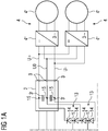
- a rectifier circuit 1 has a rectifier 2.
- the rectifier 2 has at least three outputs 3.
- the outputs 3 are usually connected to one another via backup capacitors 3 '.
- the rectifier 2 provides a potential U +, UO, U- at each of the outputs 3.
- the provided potentials U +, UO, U- are direct voltage potentials.
- the potential U + is the highest potential provided by the rectifier 2. It is referred to below as high potential U +.
- the potential U- is the lowest potential provided by the rectifier 2. It is referred to below as the low potential U-. All other potentials UO provided by the rectifier 2 - here only a single potential UO - lie between the high potential U + and the low potential U-. In the following, they are referred to as the mean potentials UO.
- the potentials U +, UO, U- are fed to loads 4.
- the loads 4 can according to the representation in FIG 1 For example, each be designed as electrical machines 4 'which are each fed via a frequency converter 4 ′′.
- the loads 4 can, however, also be designed differently.
- the loads 4 are not the subject of the present invention.
- the rectifier circuit 1 has several feed lines 5. Phase voltages L1, L2, L3 of a supply network 6 are fed to the rectifier 2 via the feed lines 5. In the feed lines 5, filter elements 7 are arranged towards the supply network 6. The filter elements 7 can be designed as throttles or comprise throttles. The supply network 6 and the filter elements 7 as such are not the subject of the present invention. Furthermore, 5 chokes 8 are arranged in the feed lines. The phase voltages L1, L2, L3 fed to the rectifier 2 are thus fed to the rectifier 2 via the respective choke 8. The chokes 8 are part of the rectifier circuit 1.
- the rectifier 2 can, for example, as shown in FIG FIG 2 Have diodes 9.
- the phase voltages L1, L2, L3 fed to the rectifier 2 are rectified by means of the diodes 9.
- the high and low potentials U +, U- are generated.
- the rectifier 2 has bidirectional electronic switching devices. Usually show the electronic switching devices as shown in FIG 2 two electronic switches 10 connected in series, for example IGBTs or FETs.
- the electronic switches 10 diodes 11 can be connected in parallel.
- the diodes 11 can alternatively be independent components or intrinsic elements of the electronic switches 10. By means of the electronic electronic switching devices, the average potential UO is made available on the basis of a corresponding control.
- the rectifier 2 can be used as shown in FIG FIG 3 instead of the diodes 9 or in parallel with the diodes 9 have electronic switches 12, for example IGBTs or FETs. If they are still present, the diodes 9 can alternatively be independent components or intrinsic elements of the electronic switches 12.
- the electronic switch 12 By means of the electronic switch 12, the high and the low potential U +, U- are provided on the basis of a corresponding control. Furthermore - are analogous to FIG 2 -
- the electronic switching devices are available, by means of which the mean potential UO is provided.
- the rectifier circuit 1 furthermore has a number of clamping circuits 13. At least one single clamping circuit 13 is present. However, several clamping circuits 13 can also be present. In particular, according to the representation in FIG 1 a clamping circuit 13 may be present for each two successive potentials U +, UO or U0, U- provided. If there are several clamping circuits 13, they are generally designed to be identical to one another. Only one of the clamping circuits 13 will therefore be explained in more detail below.
- the clamping circuit 13 has a series connection of two diode circuits 14.
- the two diode circuits 14 of the clamping circuit 13 can each be individual diodes or series connections or parallel connections of diodes.
- End points 15 of the series circuit mentioned are each connected to an output 3 at which the rectifier 2 provides one of the potentials U +, UO, U-.
- One of the outputs 3 is that output 3 at which the rectifier 2 provides the mean potential UO.
- Another of the outputs 3 is that output 3 at which the rectifier 2 provides the high potential U + or the low potential U-.
- the rectifier 2 has more than three outputs 3 and consequently also provides more than three potentials U +, UO, U-, however, two outputs 3 can also be connected to one another via the series connection of the diode circuits 14, which provide two different mean potentials UO.
- the two outputs 3, which are connected to one another via the series connection of the diode circuits 14, preferably provide immediately adjacent potentials U +, UO, U-.
- the rectifier 2 therefore preferably does not provide any potential that lies between the two potentials U +, UO or UO, U-, the corresponding outputs 3 of which are connected to one another via the series connection of the diode circuits 14.
- the clamping circuit 11 also has an overall capacitor circuit 16.
- a node 17 is connected to a reference potential PE, for example to ground or earth, via the overall capacitor circuit 16.
- the node 17 is in turn arranged between the two diode circuits 14.
- the overall capacitor circuit 16 It is possible for the overall capacitor circuit 16 to be connected directly to the reference potential PE. According to the representation in FIG 1 however, the overall capacitor circuit 16 has a number of series circuits which in turn each consist of two partial capacitor circuits 18, 19. One partial capacitor circuit 18 of such a series circuit connects the node 17 to a line section of one of the feed lines 5. The other partial capacitor circuit 19 of such a series circuit connects the same line section to the reference potential PE.
- the line section is selected in such a way that the throttle 8 of the corresponding feed line 5 is arranged between the rectifier 2 and said line section.
- the overall capacitor circuit 16 is designed symmetrically in the sense that for each phase voltage L1, L2, L3 there is one such series circuit, which in turn consists of two partial capacitor circuits 18, 19. However, this is not absolutely necessary.
- a rectifier 2 has at least three outputs 3 at which the rectifier 2 provides a high potential U +, a low potential U- and at least one medium potential UO.
- Phase voltages L1, L2, L3 of a supply network 6 can be fed to the rectifier 2 via feed lines 5.
- Chokes 8 are arranged in the feed lines 5.
- a clamping circuit 13 has two diode circuits 14 connected in series. One of the end points 15 of the series circuit is connected to an output 3 at which the rectifier 2 provides one of the average potentials UO. The other end point 15 is connected to another output 3.
- the node 17 is connected to a reference potential PE via an overall capacitor circuit 16.
- the present invention has many advantages. Due to the use of a rectifier circuit 1 which, in addition to the high potential U + and the low potential U-, also provides the average potential UO, the exciting common-mode voltage is already significantly reduced.
- the clamping circuit 13 can continue to allow potential jumps to half the potential difference between the two potentials U +, UO or UO, U- are limited, which are connected to one another via the clamping circuit 13. In this way, in particular, the voltage load on the insulation of the electrical machines 4 'can again be significantly reduced.
- the solution is robust and can be implemented cost-effectively.
- the energy that is stored in the parasitic capacitances of the lines between the rectifier circuit 1 and the loads 4 is for the most part fed back into the intermediate circuit. As a result, the efficiency of the overall circuit is improved, especially with long such lines.
Landscapes
- Engineering & Computer Science (AREA)
- Power Engineering (AREA)
- Physics & Mathematics (AREA)
- Electromagnetism (AREA)
- Rectifiers (AREA)
Abstract
Ein Gleichrichter (2) weist mindestens drei Ausgänge (3) auf, an denen der Gleichrichter (2) ein hohes Potenzial (U+), ein niedriges Potenzial (U-) und mindestens ein mittleres Potenzial (U0) bereitstellt. Über Speiseleitungen (5) sind dem Gleichrichter (2) Phasenspannungen (L1, L2, L3) eines Versorgungsnetzes (6) zuführbar. In den Speiseleitungen (5) sind Drosseln (8) angeordnet. Eine Clampingschaltung (13) weist zwei in Reihe geschaltete Diodenschaltungen (14) auf. Einer der Endpunkte (15) der Reihenschaltung ist mit einem Ausgang (3) verbunden, an dem der Gleichrichter (2) eines der mittleren Potenziale (U0) bereitstellt. Der andere Endpunkt (15) ist mit einem anderen Ausgang (3) verbunden. Über eine Gesamt-Kondensatorschaltung (16) ist der Knotenpunkt (17) mit einem Referenzpotenzial (PE) verbunden.A rectifier (2) has at least three outputs (3) at which the rectifier (2) provides a high potential (U +), a low potential (U-) and at least one medium potential (U0). Phase voltages (L1, L2, L3) of a supply network (6) can be fed to the rectifier (2) via feed lines (5). Chokes (8) are arranged in the feed lines (5). A clamping circuit (13) has two series-connected diode circuits (14). One of the end points (15) of the series circuit is connected to an output (3) at which the rectifier (2) provides one of the average potentials (U0). The other end point (15) is connected to another output (3). The node (17) is connected to a reference potential (PE) via an overall capacitor circuit (16).
Description
Die vorliegende Erfindung geht aus von einer Gleichrichterschaltung,
- wobei die Gleichrichterschaltung einen Gleichrichter aufweist,
- wobei der Gleichrichter mindestens drei Ausgänge aufweist, an denen der Gleichrichter jeweils ein Potenzial bereitstellt,
- wobei eines der bereitgestellten Potenziale ein hohes Potenzial ist, das höher als alle anderen bereitgestellten Potenziale ist,
- wobei ein weiteres der bereitgestellten Potenziale ein niedriges Potenzial ist, das niedriger als alle anderen bereitgestellten Potenziale ist,
- wobei die bereitgestellten Potenziale mit Ausnahme des hohen Potenzials und des niedrigen Potenzials mittlere Potenziale sind, die zwischen dem hohen und dem niedrigen Potenzial liegen,
- wobei die Gleichrichterschaltung mehrere Speiseleitungen aufweist, über die dem Gleichrichter jeweils eine Phasenspannung eines Versorgungsnetzes zuführbar ist,
- wobei die Gleichrichterschaltung in den Speiseleitungen angeordnete Drosseln aufweist.
- wherein the rectifier circuit comprises a rectifier,
- wherein the rectifier has at least three outputs, at which the rectifier provides a potential,
- where one of the provided potentials is a high potential that is higher than all other provided potentials,
- where another of the provided potentials is a low potential, which is lower than all other provided potentials,
- With the exception of the high potential and the low potential, the provided potentials are medium potentials that lie between the high and the low potential,
- wherein the rectifier circuit has several feed lines via which a phase voltage of a supply network can be fed to the rectifier,
- wherein the rectifier circuit has chokes arranged in the feed lines.
Derartige Gleichrichterschaltungen sind allgemein bekannt.Such rectifier circuits are generally known.
Beispielsweise sind sogenannte Vienna-Rectifier bekannt. Bei einem Vienna-Rectifier ist ein Brückengleichrichter vorhanden, dessen gleichrichtende Elemente als Dioden ausgebildet sind. Mittels des Brückengleichrichters werden das hohe und das niedrige Potenzial bereitgestellt. Weiterhin sind die Phasenspannungen innerhalb des Vienna-Rectifiers über eine jeweilige bidirektional schaltbare Schalteinrichtung mit dem Ausgang für das mittlere Potenzial verbunden. Die jeweilige bidirektional schaltbare Schalteinrichtung kann beispielsweise als Reihenschaltung von zwei Halbleiter-Schaltelementen ausgebildet sein, beispielsweise Bipolar- oder FeldeffektTransistoren.For example, so-called Vienna rectifiers are known. A Vienna rectifier has a bridge rectifier, the rectifying elements of which are designed as diodes. The high and low potential are provided by means of the bridge rectifier. Furthermore, the phase voltages within the Vienna rectifier are connected to the output for the mean potential via a respective bidirectionally switchable switching device. The respective Bidirectionally switchable switching device can, for example, be designed as a series connection of two semiconductor switching elements, for example bipolar or field effect transistors.
Weiterhin sind sogenannte 3L-Gleichrichter (3L steht für 3 Level) bekannt. Bei einem 3L-Gleichrichter ist ein Brückengleichrichter vorhanden, dessen gleichrichtende Elemente als schaltbare Elemente (meist Transistoren) ausgebildet sind. Weiterhin sind die Phasenspannungen innerhalb des 3L-Gleichrichters über bidirektional schaltbare Schalteinrichtungen mit dem Ausgang für das mittlere Potenzial verbunden.So-called 3L rectifiers (3L stands for 3 levels) are also known. A 3L rectifier has a bridge rectifier whose rectifying elements are designed as switchable elements (mostly transistors). Furthermore, the phase voltages within the 3L rectifier are connected to the output for the average potential via bidirectionally switchable switching devices.
Weiterhin sind auch Multilevelgleichrichter bekannt, also Gleichrichter, die ausgangsseitig mehr als drei Potenziale bereitstellen.Furthermore, multilevel rectifiers are also known, that is to say rectifiers which provide more than three potentials on the output side.
Die Gleichrichterschaltung speist oftmals einen Zwischenkreis, aus dem heraus wiederum Lasten gespeist werden. Beispielsweise können über Frequenzumrichter elektrische Antriebe mit Wechselstrom variabler Amplitude und variabler Frequenz gespeist werden. Beim Betrieb der Lasten können beispielsweise in den Leitungen von der Gleichrichterschaltung zu den Lasten hochfrequente Störungen auftreten, die ihrerseits Rückwirkungen auf die Gleichrichterschaltung und auch auf die angeschlossenen Lasten haben können. Beispielsweise bilden die Leitungen von der Gleichrichterschaltung zu den Lasten parasitäre Kapazitäten, welche in Verbindung mit den eingangsseitigen Drosseln der Gleichrichterschaltung in Resonanz treten können. Dies kann einen sogenannten Gleichtaktstrom bewirken, der durch die Verluste in den Drosseln oftmals nur unzureichend gedämpft wird. Dadurch kann es zu einer Spannungsüberhöhung zwischen dem Gleichspannungszwischenkreis und dem Referenzpotenzial (beispielsweise Erde) kommen. Unabhängig von der Art der Störung ist die Störung jedoch oftmals von Nachteil und sollte so weit wie möglich unterdrückt oder zumindest gering gehalten werden.The rectifier circuit often feeds an intermediate circuit from which loads are in turn fed. For example, electrical drives with alternating current of variable amplitude and variable frequency can be fed via frequency converters. When operating the loads, for example, high-frequency interference can occur in the lines from the rectifier circuit to the loads, which in turn can have repercussions on the rectifier circuit and also on the connected loads. For example, the lines from the rectifier circuit to the loads form parasitic capacitances which, in conjunction with the input-side chokes of the rectifier circuit, can come into resonance. This can cause a so-called common-mode current, which is often only insufficiently attenuated by the losses in the chokes. This can lead to an excessive voltage increase between the DC link and the reference potential (e.g. earth). Regardless of the type of disturbance, however, the disturbance is often a disadvantage and should be suppressed as far as possible or at least kept to a minimum.
Im Stand der Technik wird zur stärkeren Dämpfung des Gleichtaktstroms oftmals eine passive Dämpfung eingesetzt. Zu diesem Zweck werden den eingangsseitigen Drosseln der Gleichrichterschaltung Hilfswicklungen zugeordnet. Die Hilfswicklungen werden miteinander sowie einem Widerstand in Reihe geschaltet. Die Hilfswicklungen dämpfen nur die Gleichtaktschwingungen. Nachteilig bei dieser Lösung sind zum einen die relativ hohen Verlustleistungen, die zu einer Reduzierung des Wirkungsgrades und zu Problemen beim Abführen der auftretenden Wärme führen können. Ein weiterer Nachteil sind die relativ hohen Kosten.In the prior art, passive attenuation is often used for greater attenuation of the common-mode current. For this purpose, auxiliary windings are assigned to the input-side chokes of the rectifier circuit. The auxiliary windings are connected in series with one another and a resistor. The auxiliary windings only dampen the common mode oscillations. The disadvantage of this solution is, on the one hand, the relatively high power losses, which can lead to a reduction in the degree of efficiency and to problems in removing the heat that occurs. Another disadvantage is the relatively high cost.
Im Stand der Technik ist bei 2L-Gleichrichtern - also bei Gleichrichtern, bei denen der Gleichrichter exakt zwei Ausgänge aufweist, an denen der Gleichrichter ein hohes und ein niedriges Potenzial bereitstellt - weiterhin eine sogenannte Clampingschaltung bekannt. Diese Clampingschaltung weist eine Reihenschaltung von zwei Diodenschaltungen auf, so dass die Reihenschaltung einen zwischen den beiden Diodenschaltungen angeordneten Knotenpunkt und zwei Endpunkte aufweist. Je einer der beiden Endpunkte ist mit einem der beiden Ausgänge des Gleichrichters verbunden. Der Knotenpunkt ist über eine Gesamt-Kondensatorschaltung der Clampingschaltung mit einem Referenzpotenzial verbunden. Die Clampingschaltung begrenzt ein Springen des hohen Potenzials und des niedrigen Potenzials relativ zu dem Referenzpotenzial auf die Hälfte der Potenzialdifferenz zwischen dem hohen und dem niedrigen Potenzial.In the prior art, a so-called clamping circuit is also known in the case of 2L rectifiers - that is to say in the case of rectifiers in which the rectifier has exactly two outputs at which the rectifier provides a high and a low potential. This clamping circuit has a series connection of two diode circuits, so that the series connection has a node arranged between the two diode circuits and two end points. One of the two end points is connected to one of the two outputs of the rectifier. The node is connected to a reference potential via an overall capacitor circuit of the clamping circuit. The clamping circuit limits jumping of the high potential and the low potential relative to the reference potential to half the potential difference between the high and the low potential.
Die Aufgabe der vorliegenden Erfindung besteht darin, eine Gleichrichterschaltung der eingangs genannten Art derart weiterzuentwickeln, dass Störungen, insbesondere ein Gleichtaktstrom, mit möglichst geringem Aufwand so weit wie möglich reduziert und unterdrückt werden können.The object of the present invention is to further develop a rectifier circuit of the type mentioned at the beginning in such a way that interference, in particular a common-mode current, can be reduced and suppressed as far as possible with as little effort as possible.
Die Aufgabe wird durch eine Gleichrichterschaltung mit den Merkmalen des Anspruchs 1 gelöst. Vorteilhafte Ausgestaltungen der Gleichrichterschaltung sind Gegenstand der abhängigen Ansprüche 2 und 3.The object is achieved by a rectifier circuit having the features of claim 1. Advantageous configurations the rectifier circuit are the subject of
Erfindungsgemäß wird eine Gleichrichterschaltung der eingangs genannten Art dadurch ausgestaltet,
- dass die Gleichrichterschaltung mindestens eine Clampingschaltung aufweist,
- dass die Clampingschaltung eine Reihenschaltung von zwei Diodenschaltungen aufweist, so dass die Reihenschaltung einen zwischen den beiden Diodenschaltungen angeordneten Knotenpunkt und zwei Endpunkte aufweist,
- dass einer der Endpunkte mit einem der Ausgänge verbunden ist, an denen der Gleichrichter eines der mittleren Potenziale bereitstellt,
- dass der andere Endpunkt mit einem anderen der Ausgänge verbunden ist und
- dass die Clampingschaltung eine Gesamt-Kondensatorschaltung aufweist, über die der Knotenpunkt mit einem Referenzpotenzial verbunden ist.
- that the rectifier circuit has at least one clamping circuit,
- that the clamping circuit has a series connection of two diode circuits, so that the series connection has a node arranged between the two diode circuits and two end points,
- that one of the end points is connected to one of the outputs at which the rectifier provides one of the medium potentials,
- that the other endpoint is connected to another of the outputs and
- that the clamping circuit has an overall capacitor circuit via which the node is connected to a reference potential.
Die Gleichrichterschaltung wird also vom Ansatz her um eine Campingschaltung ergänzt, wie sie für einen 2L-Gleichrichter bekannt ist. Die Endpunkte der Diodenschaltung der Clampingschaltung werden aber nicht mit den Ausgängen für das hohe und das niedrige Potenzial verbunden, sondern mit einem der Ausgänge, an denen der Gleichrichter eines der mittleren Potenziale bereitstellt, und einem weiteren Ausgang. Der weitere Ausgang kann zwar einer der beiden Ausgänge sein, an denen der Gleichrichter das hohe und das niedrige Potenzial bereitstellt. Mindestens einer der beiden über die Clampingschaltung miteinander verbundenen Ausgänge ist jedoch von diesen beiden Ausgängen verschieden. Die von der Clampingschaltung überbrückte Potenzialdifferenz ist daher kleiner als Potenzialdifferenz zwischen dem hohen und dem niedrigen Potenzial. Die Clampingschaltung begrenzt ein Springen der von der Gleichrichterschaltung bereitgestellten Potenziale (einschließlich des hohen Potenzials und des niedrigen Potenzials) relativ zu dem Referenzpotenzial auf die Hälfte der Potenzialdifferenz zwischen den beiden Potenzialen der beiden Ausgänge, die über die Diodenschaltung der Clampingschaltung miteinander verbunden sind.The rectifier circuit is therefore supplemented by a camping circuit, as is known for a 2L rectifier. The end points of the diode circuit of the clamping circuit, however, are not connected to the outputs for the high and the low potential, but to one of the outputs at which the rectifier provides one of the medium potentials and a further output. The other output can be one of the two outputs at which the rectifier provides the high and the low potential. However, at least one of the two outputs connected to one another via the clamping circuit is different from these two outputs. The potential difference bridged by the clamping circuit is therefore smaller than the potential difference between the high and the low potential. The clamping circuit limits jumping of the potentials provided by the rectifier circuit (including the high potential and the low potential) relative to the reference potential to half the potential difference between the two potentials of the two outputs, which are connected to one another via the diode circuit of the clamping circuit.
In einer bevorzugten Ausgestaltung ist vorgesehen,
- dass die Gesamt-Kondensatorschaltung mindestens eine Reihenschaltung aufweist, die aus zwei Teil-Kondensatorschaltungen besteht,
- dass die eine Teil-Kondensatorschaltung den Knotenpunkt mit einem Leitungsabschnitt einer der Speiseleitungen verbindet,
- dass die andere Teil-Kondensatorschaltung denselben Leitungsabschnitt mit dem Referenzpotenzial verbindet und
- dass die in der entsprechenden Speiseleitung angeordnete Drossel zwischen dem Gleichrichter und dem Leitungsabschnitt angeordnet ist.
- that the overall capacitor circuit has at least one series circuit which consists of two partial capacitor circuits,
- that the one partial capacitor circuit connects the junction with a line section of one of the feed lines,
- that the other partial capacitor circuit connects the same line section to the reference potential and
- that the choke arranged in the corresponding feed line is arranged between the rectifier and the line section.
Diese Ausgestaltung nutzt den Umstand, dass die Teil-Kondensatorschaltung, die einen Leitungsabschnitt mit dem Referenzpotenzial verbindet, aus anderen Gründen oftmals bereits vorhanden ist. Sie bringt insbesondere den Vorteil mit sich, dass innerhalb der Gleichrichterschaltung nur eine einzelne Anschaltung an das Referenzpotenzial erforderlich ist. Anderenfalls würden zwei Anschaltungen existieren, was oftmals wiederum zu Problemen führen kann.This refinement makes use of the fact that the partial capacitor circuit which connects a line section to the reference potential is often already present for other reasons. It has the particular advantage that only a single connection to the reference potential is required within the rectifier circuit. Otherwise there would be two connections, which in turn can often lead to problems.
Es ist möglich, dass die Gesamt-Kondensatorschaltung direkt, also ohne zwischengeschaltete Elemente, mit dem Knotenpunkt zwischen den beiden Diodenschaltungen verbunden ist. Vorzugsweise ist aber vorgesehen,
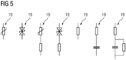
- dass die Clampingschaltung ein Schaltungsnetzwerk aufweist,
- dass das Schaltungsnetzwerk zwischen dem Knotenpunkt und der Gesamt-Kondensatorschaltung angeordnet ist und
- dass das Schaltungsnetzwerk einen Varistor mit einem oder ohne einen in Reihe geschalteten Widerstand, eine Zenerdiode mit einem oder ohne einen in Reihe geschalteten Widerstand, einen Dämpfungswiderstand oder eine Reihenschaltung eines Widerstandes und eines Kondensators mit einem oder ohne einen den Kondensator überbrückenden Widerstand aufweist.
- that the clamping circuit has a circuit network,
- that the circuit network is arranged between the node and the overall capacitor circuit and
- that the circuit network comprises a varistor with or without a series-connected resistor, a Zener diode with or without a series-connected resistor, a damping resistor or a series connection of a resistor and a capacitor with an or without a resistor bridging the capacitor.
Durch diese Ausgestaltung können insbesondere ein Feintuning des Verhaltens der Clampingschaltung und eine Reduzierung des über die Clampingschaltung fließenden Stromes erreicht werden.This refinement makes it possible, in particular, to fine-tune the behavior of the clamping circuit and to reduce the current flowing through the clamping circuit.
Die oben beschriebenen Eigenschaften, Merkmale und Vorteile dieser Erfindung sowie die Art und Weise, wie diese erreicht werden, werden klarer und deutlicher verständlich im Zusammenhang mit der folgenden Beschreibung der Ausführungsbeispiele, die in Verbindung mit den Zeichnungen näher erläutert werden. Hierbei zeigen in schematischer Darstellung:
- FIG 1
- eine Gleichrichterschaltung und ergänzende Komponenten,
- FIG 2
- eine mögliche Ausgestaltung eines Gleichrichters,
- FIG 3
- eine weitere mögliche Ausgestaltung eines Gleichrichters,
- FIG 4
- eine Modifikation der Gleichrichterschaltung von
FIG 1 und - FIG 5
- mögliche Ausgestaltungen eines Schaltungsnetzwerks.
- FIG 1
- a rectifier circuit and additional components,
- FIG 2
- a possible design of a rectifier,
- FIG 3
- another possible design of a rectifier,
- FIG 4
- a modification of the rectifier circuit of
FIG 1 and - FIG 5
- possible configurations of a circuit network.
Gemäß
Die Potenziale U+, UO, U- werden Lasten 4 zugeführt. Die Lasten 4 können entsprechend der Darstellung in
Die Gleichrichterschaltung 1 weist mehrere Speiseleitungen 5 aufweist. Über die Speiseleitungen 5 werden dem Gleichrichter 2 Phasenspannungen L1, L2, L3 eines Versorgungsnetzes 6 zugeführt. In den Speiseleitungen 5 sind zum Versorgungsnetz 6 hin Filterelemente 7 angeordnet. Die Filterelemente 7 können als Drosseln ausgebildet sein oder Drosseln umfassen. Das Versorgungsnetz 6 und die Filterelemente 7 sind als solche nicht Gegenstand der vorliegenden Erfindung. Weiterhin sind in den Speiseleitungen 5 Drosseln 8 angeordnet. Die dem Gleichrichter 2 zugeführten Phasenspannungen L1, L2, L3 werden dem Gleichrichter 2 somit über die jeweilige Drossel 8 zugeführt. Die Drosseln 8 sind Bestandteil der Gleichrichterschaltung 1.The rectifier circuit 1 has
Für die innere Ausgestaltung des Gleichrichters 2 sind verschiedene Ausgestaltungen möglich. Nachfolgend werden mögliche Ausgestaltungen für den häufigsten Fall erläutert, bei dem der Gleichrichter 2 zusätzlich zu dem hohen und dem niedrigen Potenzial U+, U- nur ein einziges mittleres Potenzial UO bereitstellt.Various configurations are possible for the internal configuration of the
In diesem Fall kann der Gleichrichter 2 beispielsweise entsprechend der Darstellung in
Alternativ kann der Gleichrichter 2 entsprechend der Darstellung in
Sowohl der schaltungstechnische Aufbau der Gleichrichter 2 der
Gemäß
Die Clampingschaltung 13 weist eine Reihenschaltung von zwei Diodenschaltungen 14 auf. Die beiden Diodenschaltungen 14 der Clampingschaltung 13 können jeweils einzelne Dioden oder Reihenschaltungen oder Parallelschaltungen von Dioden sein.The clamping
Endpunkte 15 der genannten Reihenschaltung sind mit je einem Ausgang 3 verbunden, an dem der Gleichrichter 2 je eines der Potenziale U+, UO, U- bereitstellt. Einer der Ausgänge 3 ist derjenige Ausgang 3, an dem der Gleichrichter 2 das mittlere Potenzial UO bereitstellt. Ein weiterer der Ausgänge 3 ist derjenige Ausgang 3, an dem der Gleichrichter 2 das hohe Potenzial U+ oder das niedrige Potenzial U- bereitstellt. Im Falle der Ausgestaltung gemäß
Die Clampingschaltung 11 weist weiterhin eine Gesamt-Kondensatorschaltung 16 auf. Über die Gesamt-Kondensatorschaltung 16 ist ein Knotenpunkt 17 mit einem Referenzpotenzial PE verbunden, beispielsweise mit Masse oder Erde. Der Knotenpunkt 17 ist seinerseits zwischen den beiden Diodenschaltungen 14 angeordnet.The clamping
Es ist möglich, dass die Gesamt-Kondensatorschaltung 16 direkt mit dem Referenzpotenzial PE verbunden ist. Entsprechend der Darstellung in
In der Regel wird die Gesamt-Kondensatorschaltung 16 symmetrisch in dem Sinne ausgebildet sein, dass für jede Phasenspannung L1, L2, L3 je eine derartige Reihenschaltung vorhanden ist, die ihrerseits aus zwei Teil-Kondensatorschaltungen 18, 19 besteht. Dies ist aber nicht zwingend erforderlich.As a rule, the
Im einfachsten Fall ist die Gesamt-Kondensatorschaltung 16 direkt mit dem Knotenpunkt 17 verbunden. Es ist jedoch entsprechend der Darstellung in
- Es kann als Varistor ausgebildet sein. Ein Varistor ist, wie Fachleuten allgemein bekannt ist, ein elektrisches Bauelement, dessen Widerstand von der über dem Bauelement abfallenden elektrischen Spannung abhängig ist. Insbesondere wird der differenzielle Widerstand des Varistors oberhalb einer bestimmten Schwellenspannung rapide kleiner. Die Schwellenspannung ihrerseits ist durch die Bauart und die Auslegung des Varistors festgelegt.
- Es kann als Varistor ausgebildet sein, dem ein Widerstand in Reihe geschaltet ist.
- Es kann als Zenerdiode ausgebildet sein.
- Es kann als Zenerdiode ausgebildet sein, der ein Widerstand in Reihe geschaltet ist.
- Es kann als Dämpfungswiderstand ausgebildet sein.
- Es kann als Reihenschaltung eines Widerstandes und eines Kondensators ausgebildet sein.
- Es kann als Reihenschaltung eines Widerstandes und eines Kondensators ausgebildet sein, wobei der Kondensator zusätzlich durch einen weiteren Widerstand überbrückt ist.
- It can be designed as a varistor. As is well known to those skilled in the art, a varistor is an electrical component, the resistance of which is dependent on the electrical voltage drop across the component. In particular, the differential resistance of the varistor decreases rapidly above a certain threshold voltage. The The threshold voltage, for its part, is determined by the type and design of the varistor.
- It can be designed as a varistor with a resistor connected in series.
- It can be designed as a Zener diode.
- It can be designed as a Zener diode with a resistor connected in series.
- It can be designed as a damping resistor.
- It can be designed as a series connection of a resistor and a capacitor.
- It can be designed as a series connection of a resistor and a capacitor, the capacitor being additionally bridged by a further resistor.
Ein Gleichrichter 2 weist mindestens drei Ausgänge 3 auf, an denen der Gleichrichter 2 ein hohes Potenzial U+, ein niedriges Potenzial U- und mindestens ein mittleres Potenzial UO bereitstellt. Über Speiseleitungen 5 sind dem Gleichrichter 2 Phasenspannungen L1, L2, L3 eines Versorgungsnetzes 6 zuführbar. In den Speiseleitungen 5 sind Drosseln 8 angeordnet. Eine Clampingschaltung 13 weist zwei in Reihe geschaltete Diodenschaltungen 14 auf. Einer der Endpunkte 15 der Reihenschaltung ist mit einem Ausgang 3 verbunden, an dem der Gleichrichter 2 eines der mittleren Potenziale UO bereitstellt. Der andere Endpunkt 15 ist mit einem anderen Ausgang 3 verbunden. Über eine Gesamt-Kondensatorschaltung 16 ist der Knotenpunkt 17 mit einem Referenzpotenzial PE verbunden.A
Die vorliegende Erfindung weist viele Vorteile auf. Aufgrund der Verwendung einer Gleichrichterschaltung 1, welche zusätzlich zu dem hohen Potenzial U+ und dem niedrigen Potenzial U-auch das mittlere Potenzial UO bereitstellt, ist die anregende Gleichtaktspannung bereits deutlich verringert. Durch die Clampingschaltung 13 können weiterhin Potenzialsprünge auf die Hälfte der Potenzialdifferenz der beiden Potenziale U+, UO bzw. UO, U- begrenzt werden, die über die Clampingschaltung 13 miteinander verbunden sind. Dadurch kann insbesondere die Spannungsbelastung an der Isolierung der elektrischen Maschinen 4' nochmals deutlich reduziert werden. Die Lösung ist robust und kostengünstig realisierbar. Die Energie, die in den parasitären Kapazitäten der Leitungen zwischen der Gleichrichterschaltung 1 und den Lasten 4 gespeichert wird, wird zum größten Teil zurück in den Zwischenkreis geführt. Dadurch wird der Wirkungsgrad der Gesamtschaltung insbesondere bei langen derartigen Leitungen verbessert.The present invention has many advantages. Due to the use of a rectifier circuit 1 which, in addition to the high potential U + and the low potential U-, also provides the average potential UO, the exciting common-mode voltage is already significantly reduced. The clamping
Obwohl die Erfindung im Detail durch das bevorzugte Ausführungsbeispiel näher illustriert und beschrieben wurde, so ist die Erfindung nicht durch die offenbarten Beispiele eingeschränkt und andere Variationen können vom Fachmann hieraus abgeleitet werden, ohne den Schutzumfang der Erfindung zu verlassen.Although the invention has been illustrated and described in more detail by the preferred exemplary embodiment, the invention is not restricted by the disclosed examples and other variations can be derived therefrom by the person skilled in the art without departing from the scope of protection of the invention.
Claims (3)
dadurch gekennzeichnet,
characterized,
dadurch gekennzeichnet,
characterized,
dadurch gekennzeichnet,
characterized,
Priority Applications (5)
| Application Number | Priority Date | Filing Date | Title |
|---|---|---|---|
| EP19199206.4A EP3799283A1 (en) | 2019-09-24 | 2019-09-24 | Clamp circuit in a rectifier with more than two output potentials |
| PCT/EP2020/072082 WO2021058187A1 (en) | 2019-09-24 | 2020-08-06 | Clamping circuit in a rectifier with more than two potentials provided on the output side |
| EP20763987.3A EP3987637B1 (en) | 2019-09-24 | 2020-08-06 | Clamp circuit in a rectifier with more than two output potentials |
| US17/763,079 US11973434B2 (en) | 2019-09-24 | 2020-08-06 | Clamping circuit in a rectifier with more than two potentials provided on the output side |
| CN202080066720.1A CN114503412A (en) | 2019-09-24 | 2020-08-06 | Clamping circuit in a rectifier with more than two potentials provided at the output |
Applications Claiming Priority (1)
| Application Number | Priority Date | Filing Date | Title |
|---|---|---|---|
| EP19199206.4A EP3799283A1 (en) | 2019-09-24 | 2019-09-24 | Clamp circuit in a rectifier with more than two output potentials |
Publications (1)
| Publication Number | Publication Date |
|---|---|
| EP3799283A1 true EP3799283A1 (en) | 2021-03-31 |
Family
ID=68066611
Family Applications (2)
| Application Number | Title | Priority Date | Filing Date |
|---|---|---|---|
| EP19199206.4A Withdrawn EP3799283A1 (en) | 2019-09-24 | 2019-09-24 | Clamp circuit in a rectifier with more than two output potentials |
| EP20763987.3A Active EP3987637B1 (en) | 2019-09-24 | 2020-08-06 | Clamp circuit in a rectifier with more than two output potentials |
Family Applications After (1)
| Application Number | Title | Priority Date | Filing Date |
|---|---|---|---|
| EP20763987.3A Active EP3987637B1 (en) | 2019-09-24 | 2020-08-06 | Clamp circuit in a rectifier with more than two output potentials |
Country Status (4)
| Country | Link |
|---|---|
| US (1) | US11973434B2 (en) |
| EP (2) | EP3799283A1 (en) |
| CN (1) | CN114503412A (en) |
| WO (1) | WO2021058187A1 (en) |
Citations (3)
| Publication number | Priority date | Publication date | Assignee | Title |
|---|---|---|---|---|
| DE102010008426A1 (en) * | 2010-02-18 | 2011-08-18 | Hochschule Konstanz, 78462 | 3-stage pulse inverter with discharge network |
| DE102012005622A1 (en) * | 2012-03-22 | 2013-09-26 | Sew-Eurodrive Gmbh & Co. Kg | Circuit arrangement and arrangement of capacitors |
| DE102013112538A1 (en) * | 2013-11-14 | 2015-05-21 | Sma Solar Technology Ag | Method and inverter for determining capacitance values of capacities of a power supply system |
Family Cites Families (3)
| Publication number | Priority date | Publication date | Assignee | Title |
|---|---|---|---|---|
| WO2009076771A1 (en) * | 2007-12-19 | 2009-06-25 | Phoster Industries | Creating and modifying a colored shadow |
| US10594227B1 (en) * | 2019-03-22 | 2020-03-17 | Hamilton Sundstrand Corporation | Matrix converter operating in current control mode using feed forward signals |
| US11689115B2 (en) * | 2020-10-02 | 2023-06-27 | The Research Foundation for the State University o | Bidirectional AC-DC converter with multilevel power factor correction |
-
2019
- 2019-09-24 EP EP19199206.4A patent/EP3799283A1/en not_active Withdrawn
-
2020
- 2020-08-06 EP EP20763987.3A patent/EP3987637B1/en active Active
- 2020-08-06 WO PCT/EP2020/072082 patent/WO2021058187A1/en active Search and Examination
- 2020-08-06 US US17/763,079 patent/US11973434B2/en active Active
- 2020-08-06 CN CN202080066720.1A patent/CN114503412A/en active Pending
Patent Citations (3)
| Publication number | Priority date | Publication date | Assignee | Title |
|---|---|---|---|---|
| DE102010008426A1 (en) * | 2010-02-18 | 2011-08-18 | Hochschule Konstanz, 78462 | 3-stage pulse inverter with discharge network |
| DE102012005622A1 (en) * | 2012-03-22 | 2013-09-26 | Sew-Eurodrive Gmbh & Co. Kg | Circuit arrangement and arrangement of capacitors |
| DE102013112538A1 (en) * | 2013-11-14 | 2015-05-21 | Sma Solar Technology Ag | Method and inverter for determining capacitance values of capacities of a power supply system |
Non-Patent Citations (1)
| Title |
|---|
| CHRISTOPH HAMMERSCHMIDT: "Soft switching: Better efficiency for high power inverters", 11 April 2016 (2016-04-11), XP002798481, Retrieved from the Internet <URL:https://www.eenewspower.com/news/soft-switching-better-efficiency-high-power-inverters> [retrieved on 20200326] * |
Also Published As
| Publication number | Publication date |
|---|---|
| WO2021058187A1 (en) | 2021-04-01 |
| US20220407434A1 (en) | 2022-12-22 |
| EP3987637B1 (en) | 2023-05-31 |
| US11973434B2 (en) | 2024-04-30 |
| EP3987637A1 (en) | 2022-04-27 |
| CN114503412A (en) | 2022-05-13 |
Similar Documents
| Publication | Publication Date | Title |
|---|---|---|
| DE19710319B4 (en) | Circuit for blocking a semiconductor switching device in the event of overcurrent | |
| EP0298562B1 (en) | Circuit arrangement for the transmission of electric energy | |
| DE3325612C2 (en) | ||
| EP0899859B1 (en) | Intermediate voltage link inverter | |
| DE112012005768T5 (en) | High-frequency current reduction device | |
| DE19757452A1 (en) | Current converter circuit arrangement | |
| DE112016003290T5 (en) | POWER CONVERTER | |
| EP0682402B1 (en) | Output magnitudes rise limiting device for self-commutated constant voltage intermediate circuit converter | |
| DE10062075A1 (en) | Converter with integrated DC link capacitors | |
| EP0682401B1 (en) | Limiting device for the output voltage slope of a self-commutated converter | |
| EP3251194B1 (en) | Energy storage arrangement | |
| DE19607201A1 (en) | Anti-HF-noise filter for voltage source inverter | |
| EP3987637B1 (en) | Clamp circuit in a rectifier with more than two output potentials | |
| DE10314514B4 (en) | Power device control circuit | |
| WO2001039347A1 (en) | Protective device against overpotential in the terminals of electrical equipment, caused by switching operations | |
| AT504961B1 (en) | CIRCUIT ARRANGEMENT FOR REDUCED SWITCH LOAD | |
| DE102017217483A1 (en) | Converter and system with an electric drive and a converter | |
| EP3850739B1 (en) | Electrical supply device and method for operating an electrical supply device | |
| DE3036092A1 (en) | BATTERY CHARGING SYSTEM | |
| AT514765B1 (en) | Circuit for limiting common-mode voltages | |
| DE4106045C1 (en) | Multi-phase semiconductor three-stage AC inverter - has low inductance capacitors which limit sheet duration voltage transients | |
| DE10204040A1 (en) | Method for operating an intermediate circuit voltage changer, e.g. for electric motor controller, uses phased power supply in sinusoidal operation on earthed mains system | |
| DE102016004331A1 (en) | Circuit arrangement for limiting a load current | |
| DE102012205080A1 (en) | Method for controlling insulated gate bipolar transistor of three-level converter, involves deriving unacceptable error state to protect transistors by rate pulse pattern in accordance with pulse pattern changed to unimpaired operation | |
| DE102010027866A1 (en) | Link voltage-converter has link-condenser with slight link and current supply-unit that has buffer condenser, where series connection has current-limiting component |
Legal Events
| Date | Code | Title | Description |
|---|---|---|---|
| PUAI | Public reference made under article 153(3) epc to a published international application that has entered the european phase |
Free format text: ORIGINAL CODE: 0009012 |
|
| STAA | Information on the status of an ep patent application or granted ep patent |
Free format text: STATUS: THE APPLICATION HAS BEEN PUBLISHED |
|
| AK | Designated contracting states |
Kind code of ref document: A1 Designated state(s): AL AT BE BG CH CY CZ DE DK EE ES FI FR GB GR HR HU IE IS IT LI LT LU LV MC MK MT NL NO PL PT RO RS SE SI SK SM TR |
|
| AX | Request for extension of the european patent |
Extension state: BA ME |
|
| STAA | Information on the status of an ep patent application or granted ep patent |
Free format text: STATUS: THE APPLICATION IS DEEMED TO BE WITHDRAWN |
|
| 18D | Application deemed to be withdrawn |
Effective date: 20211001 |