EP3712665A1 - Interposer-type component carrier and method of manufacturing the same - Google Patents
Interposer-type component carrier and method of manufacturing the same Download PDFInfo
- Publication number
- EP3712665A1 EP3712665A1 EP20162435.0A EP20162435A EP3712665A1 EP 3712665 A1 EP3712665 A1 EP 3712665A1 EP 20162435 A EP20162435 A EP 20162435A EP 3712665 A1 EP3712665 A1 EP 3712665A1
- Authority
- EP
- European Patent Office
- Prior art keywords
- component carrier
- component
- interposer
- layer structure
- cavity
- Prior art date
- Legal status (The legal status is an assumption and is not a legal conclusion. Google has not performed a legal analysis and makes no representation as to the accuracy of the status listed.)
- Pending
Links
Images

Classifications
-
- H—ELECTRICITY
- H10—SEMICONDUCTOR DEVICES; ELECTRIC SOLID-STATE DEVICES NOT OTHERWISE PROVIDED FOR
- H10W—GENERIC PACKAGES, INTERCONNECTIONS, CONNECTORS OR OTHER CONSTRUCTIONAL DETAILS OF DEVICES COVERED BY CLASS H10
- H10W70/00—Package substrates; Interposers; Redistribution layers [RDL]
- H10W70/60—Insulating or insulated package substrates; Interposers; Redistribution layers
- H10W70/611—Insulating or insulated package substrates; Interposers; Redistribution layers for connecting multiple chips together
- H10W70/614—Insulating or insulated package substrates; Interposers; Redistribution layers for connecting multiple chips together the multiple chips being integrally enclosed
-
- G—PHYSICS
- G02—OPTICS
- G02B—OPTICAL ELEMENTS, SYSTEMS OR APPARATUS
- G02B6/00—Light guides; Structural details of arrangements comprising light guides and other optical elements, e.g. couplings
- G02B6/10—Light guides; Structural details of arrangements comprising light guides and other optical elements, e.g. couplings of the optical waveguide type
- G02B6/12—Light guides; Structural details of arrangements comprising light guides and other optical elements, e.g. couplings of the optical waveguide type of the integrated circuit kind
-
- H—ELECTRICITY
- H05—ELECTRIC TECHNIQUES NOT OTHERWISE PROVIDED FOR
- H05K—PRINTED CIRCUITS; CASINGS OR CONSTRUCTIONAL DETAILS OF ELECTRIC APPARATUS; MANUFACTURE OF ASSEMBLAGES OF ELECTRICAL COMPONENTS
- H05K1/00—Printed circuits
- H05K1/02—Details
- H05K1/0271—Arrangements for reducing stress or warp in rigid printed circuit boards, e.g. caused by loads, vibrations or differences in thermal expansion
-
- H—ELECTRICITY
- H05—ELECTRIC TECHNIQUES NOT OTHERWISE PROVIDED FOR
- H05K—PRINTED CIRCUITS; CASINGS OR CONSTRUCTIONAL DETAILS OF ELECTRIC APPARATUS; MANUFACTURE OF ASSEMBLAGES OF ELECTRICAL COMPONENTS
- H05K1/00—Printed circuits
- H05K1/18—Printed circuits structurally associated with non-printed electric components
- H05K1/182—Printed circuits structurally associated with non-printed electric components associated with components mounted in printed circuit boards [PCB], e.g. insert-mounted components [IMC]
- H05K1/185—Printed circuits structurally associated with non-printed electric components associated with components mounted in printed circuit boards [PCB], e.g. insert-mounted components [IMC] associated with components encapsulated in the insulating substrate of the PCBs; associated with components incorporated in internal layers of multilayer circuit boards
-
- H—ELECTRICITY
- H10—SEMICONDUCTOR DEVICES; ELECTRIC SOLID-STATE DEVICES NOT OTHERWISE PROVIDED FOR
- H10W—GENERIC PACKAGES, INTERCONNECTIONS, CONNECTORS OR OTHER CONSTRUCTIONAL DETAILS OF DEVICES COVERED BY CLASS H10
- H10W20/00—Interconnections in chips, wafers or substrates
- H10W20/40—Interconnections external to wafers or substrates, e.g. back-end-of-line [BEOL] metallisations or vias connecting to gate electrodes
- H10W20/482—Interconnections external to wafers or substrates, e.g. back-end-of-line [BEOL] metallisations or vias connecting to gate electrodes for individual devices provided for in groups H10D8/00 - H10D48/00, e.g. for power transistors
- H10W20/484—Interconnections having extended contours, e.g. pads having mesh shape or interconnections comprising connected parallel stripes
-
- H—ELECTRICITY
- H10—SEMICONDUCTOR DEVICES; ELECTRIC SOLID-STATE DEVICES NOT OTHERWISE PROVIDED FOR
- H10W—GENERIC PACKAGES, INTERCONNECTIONS, CONNECTORS OR OTHER CONSTRUCTIONAL DETAILS OF DEVICES COVERED BY CLASS H10
- H10W70/00—Package substrates; Interposers; Redistribution layers [RDL]
- H10W70/01—Manufacture or treatment
- H10W70/05—Manufacture or treatment of insulating or insulated package substrates, or of interposers, or of redistribution layers
-
- H—ELECTRICITY
- H10—SEMICONDUCTOR DEVICES; ELECTRIC SOLID-STATE DEVICES NOT OTHERWISE PROVIDED FOR
- H10W—GENERIC PACKAGES, INTERCONNECTIONS, CONNECTORS OR OTHER CONSTRUCTIONAL DETAILS OF DEVICES COVERED BY CLASS H10
- H10W70/00—Package substrates; Interposers; Redistribution layers [RDL]
- H10W70/01—Manufacture or treatment
- H10W70/05—Manufacture or treatment of insulating or insulated package substrates, or of interposers, or of redistribution layers
- H10W70/08—Manufacture or treatment of insulating or insulated package substrates, or of interposers, or of redistribution layers by depositing layers on the chip or wafer, e.g. "chip-first" RDLs
- H10W70/09—Manufacture or treatment of insulating or insulated package substrates, or of interposers, or of redistribution layers by depositing layers on the chip or wafer, e.g. "chip-first" RDLs extending onto an encapsulation that laterally surrounds the chip or wafer, e.g. fan-out wafer level package [FOWLP] RDLs
-
- H—ELECTRICITY
- H10—SEMICONDUCTOR DEVICES; ELECTRIC SOLID-STATE DEVICES NOT OTHERWISE PROVIDED FOR
- H10W—GENERIC PACKAGES, INTERCONNECTIONS, CONNECTORS OR OTHER CONSTRUCTIONAL DETAILS OF DEVICES COVERED BY CLASS H10
- H10W70/00—Package substrates; Interposers; Redistribution layers [RDL]
- H10W70/01—Manufacture or treatment
- H10W70/05—Manufacture or treatment of insulating or insulated package substrates, or of interposers, or of redistribution layers
- H10W70/095—Manufacture or treatment of insulating or insulated package substrates, or of interposers, or of redistribution layers of vias therein
-
- H—ELECTRICITY
- H10—SEMICONDUCTOR DEVICES; ELECTRIC SOLID-STATE DEVICES NOT OTHERWISE PROVIDED FOR
- H10W—GENERIC PACKAGES, INTERCONNECTIONS, CONNECTORS OR OTHER CONSTRUCTIONAL DETAILS OF DEVICES COVERED BY CLASS H10
- H10W70/00—Package substrates; Interposers; Redistribution layers [RDL]
- H10W70/60—Insulating or insulated package substrates; Interposers; Redistribution layers
- H10W70/611—Insulating or insulated package substrates; Interposers; Redistribution layers for connecting multiple chips together
-
- H—ELECTRICITY
- H10—SEMICONDUCTOR DEVICES; ELECTRIC SOLID-STATE DEVICES NOT OTHERWISE PROVIDED FOR
- H10W—GENERIC PACKAGES, INTERCONNECTIONS, CONNECTORS OR OTHER CONSTRUCTIONAL DETAILS OF DEVICES COVERED BY CLASS H10
- H10W70/00—Package substrates; Interposers; Redistribution layers [RDL]
- H10W70/60—Insulating or insulated package substrates; Interposers; Redistribution layers
- H10W70/62—Insulating or insulated package substrates; Interposers; Redistribution layers characterised by their interconnections
- H10W70/63—Vias, e.g. via plugs
- H10W70/635—Through-vias
-
- H—ELECTRICITY
- H10—SEMICONDUCTOR DEVICES; ELECTRIC SOLID-STATE DEVICES NOT OTHERWISE PROVIDED FOR
- H10W—GENERIC PACKAGES, INTERCONNECTIONS, CONNECTORS OR OTHER CONSTRUCTIONAL DETAILS OF DEVICES COVERED BY CLASS H10
- H10W70/00—Package substrates; Interposers; Redistribution layers [RDL]
- H10W70/60—Insulating or insulated package substrates; Interposers; Redistribution layers
- H10W70/62—Insulating or insulated package substrates; Interposers; Redistribution layers characterised by their interconnections
- H10W70/65—Shapes or dispositions of interconnections
-
- H—ELECTRICITY
- H10—SEMICONDUCTOR DEVICES; ELECTRIC SOLID-STATE DEVICES NOT OTHERWISE PROVIDED FOR
- H10W—GENERIC PACKAGES, INTERCONNECTIONS, CONNECTORS OR OTHER CONSTRUCTIONAL DETAILS OF DEVICES COVERED BY CLASS H10
- H10W70/00—Package substrates; Interposers; Redistribution layers [RDL]
- H10W70/60—Insulating or insulated package substrates; Interposers; Redistribution layers
- H10W70/67—Insulating or insulated package substrates; Interposers; Redistribution layers characterised by their insulating layers or insulating parts
- H10W70/68—Shapes or dispositions thereof
- H10W70/685—Shapes or dispositions thereof comprising multiple insulating layers
-
- H—ELECTRICITY
- H10—SEMICONDUCTOR DEVICES; ELECTRIC SOLID-STATE DEVICES NOT OTHERWISE PROVIDED FOR
- H10W—GENERIC PACKAGES, INTERCONNECTIONS, CONNECTORS OR OTHER CONSTRUCTIONAL DETAILS OF DEVICES COVERED BY CLASS H10
- H10W70/00—Package substrates; Interposers; Redistribution layers [RDL]
- H10W70/60—Insulating or insulated package substrates; Interposers; Redistribution layers
- H10W70/67—Insulating or insulated package substrates; Interposers; Redistribution layers characterised by their insulating layers or insulating parts
- H10W70/69—Insulating materials thereof
-
- H—ELECTRICITY
- H10—SEMICONDUCTOR DEVICES; ELECTRIC SOLID-STATE DEVICES NOT OTHERWISE PROVIDED FOR
- H10W—GENERIC PACKAGES, INTERCONNECTIONS, CONNECTORS OR OTHER CONSTRUCTIONAL DETAILS OF DEVICES COVERED BY CLASS H10
- H10W72/00—Interconnections or connectors in packages
- H10W72/01—Manufacture or treatment
- H10W72/019—Manufacture or treatment of bond pads
-
- H—ELECTRICITY
- H10—SEMICONDUCTOR DEVICES; ELECTRIC SOLID-STATE DEVICES NOT OTHERWISE PROVIDED FOR
- H10W—GENERIC PACKAGES, INTERCONNECTIONS, CONNECTORS OR OTHER CONSTRUCTIONAL DETAILS OF DEVICES COVERED BY CLASS H10
- H10W72/00—Interconnections or connectors in packages
- H10W72/071—Connecting or disconnecting
-
- H—ELECTRICITY
- H10—SEMICONDUCTOR DEVICES; ELECTRIC SOLID-STATE DEVICES NOT OTHERWISE PROVIDED FOR
- H10W—GENERIC PACKAGES, INTERCONNECTIONS, CONNECTORS OR OTHER CONSTRUCTIONAL DETAILS OF DEVICES COVERED BY CLASS H10
- H10W72/00—Interconnections or connectors in packages
- H10W72/071—Connecting or disconnecting
- H10W72/072—Connecting or disconnecting of bump connectors
-
- H—ELECTRICITY
- H10—SEMICONDUCTOR DEVICES; ELECTRIC SOLID-STATE DEVICES NOT OTHERWISE PROVIDED FOR
- H10W—GENERIC PACKAGES, INTERCONNECTIONS, CONNECTORS OR OTHER CONSTRUCTIONAL DETAILS OF DEVICES COVERED BY CLASS H10
- H10W90/00—Package configurations
- H10W90/20—Configurations of stacked chips
- H10W90/293—Configurations of stacked chips characterised by non-galvanic coupling between the chips, e.g. capacitive coupling
-
- H—ELECTRICITY
- H10—SEMICONDUCTOR DEVICES; ELECTRIC SOLID-STATE DEVICES NOT OTHERWISE PROVIDED FOR
- H10W—GENERIC PACKAGES, INTERCONNECTIONS, CONNECTORS OR OTHER CONSTRUCTIONAL DETAILS OF DEVICES COVERED BY CLASS H10
- H10W90/00—Package configurations
- H10W90/701—Package configurations characterised by the relative positions of pads or connectors relative to package parts
-
- G—PHYSICS
- G02—OPTICS
- G02B—OPTICAL ELEMENTS, SYSTEMS OR APPARATUS
- G02B6/00—Light guides; Structural details of arrangements comprising light guides and other optical elements, e.g. couplings
- G02B6/10—Light guides; Structural details of arrangements comprising light guides and other optical elements, e.g. couplings of the optical waveguide type
- G02B6/12—Light guides; Structural details of arrangements comprising light guides and other optical elements, e.g. couplings of the optical waveguide type of the integrated circuit kind
- G02B2006/12035—Materials
- G02B2006/12038—Glass (SiO2 based materials)
-
- H—ELECTRICITY
- H05—ELECTRIC TECHNIQUES NOT OTHERWISE PROVIDED FOR
- H05K—PRINTED CIRCUITS; CASINGS OR CONSTRUCTIONAL DETAILS OF ELECTRIC APPARATUS; MANUFACTURE OF ASSEMBLAGES OF ELECTRICAL COMPONENTS
- H05K2201/00—Indexing scheme relating to printed circuits covered by H05K1/00
- H05K2201/09—Shape and layout
- H05K2201/09209—Shape and layout details of conductors
- H05K2201/095—Conductive through-holes or vias
- H05K2201/09636—Details of adjacent, not connected vias
-
- H—ELECTRICITY
- H05—ELECTRIC TECHNIQUES NOT OTHERWISE PROVIDED FOR
- H05K—PRINTED CIRCUITS; CASINGS OR CONSTRUCTIONAL DETAILS OF ELECTRIC APPARATUS; MANUFACTURE OF ASSEMBLAGES OF ELECTRICAL COMPONENTS
- H05K2201/00—Indexing scheme relating to printed circuits covered by H05K1/00
- H05K2201/10—Details of components or other objects attached to or integrated in a printed circuit board
- H05K2201/10227—Other objects, e.g. metallic pieces
- H05K2201/10378—Interposers
-
- H—ELECTRICITY
- H05—ELECTRIC TECHNIQUES NOT OTHERWISE PROVIDED FOR
- H05K—PRINTED CIRCUITS; CASINGS OR CONSTRUCTIONAL DETAILS OF ELECTRIC APPARATUS; MANUFACTURE OF ASSEMBLAGES OF ELECTRICAL COMPONENTS
- H05K2201/00—Indexing scheme relating to printed circuits covered by H05K1/00
- H05K2201/10—Details of components or other objects attached to or integrated in a printed circuit board
- H05K2201/10227—Other objects, e.g. metallic pieces
- H05K2201/10416—Metallic blocks or heatsinks completely inserted in a PCB
-
- H—ELECTRICITY
- H05—ELECTRIC TECHNIQUES NOT OTHERWISE PROVIDED FOR
- H05K—PRINTED CIRCUITS; CASINGS OR CONSTRUCTIONAL DETAILS OF ELECTRIC APPARATUS; MANUFACTURE OF ASSEMBLAGES OF ELECTRICAL COMPONENTS
- H05K2201/00—Indexing scheme relating to printed circuits covered by H05K1/00
- H05K2201/10—Details of components or other objects attached to or integrated in a printed circuit board
- H05K2201/10431—Details of mounted components
- H05K2201/10507—Involving several components
- H05K2201/10522—Adjacent components
-
- H—ELECTRICITY
- H10—SEMICONDUCTOR DEVICES; ELECTRIC SOLID-STATE DEVICES NOT OTHERWISE PROVIDED FOR
- H10W—GENERIC PACKAGES, INTERCONNECTIONS, CONNECTORS OR OTHER CONSTRUCTIONAL DETAILS OF DEVICES COVERED BY CLASS H10
- H10W70/00—Package substrates; Interposers; Redistribution layers [RDL]
- H10W70/01—Manufacture or treatment
- H10W70/05—Manufacture or treatment of insulating or insulated package substrates, or of interposers, or of redistribution layers
- H10W70/093—Connecting or disconnecting other interconnections thereto or therefrom, e.g. connecting bond wires or bumps
-
- H—ELECTRICITY
- H10—SEMICONDUCTOR DEVICES; ELECTRIC SOLID-STATE DEVICES NOT OTHERWISE PROVIDED FOR
- H10W—GENERIC PACKAGES, INTERCONNECTIONS, CONNECTORS OR OTHER CONSTRUCTIONAL DETAILS OF DEVICES COVERED BY CLASS H10
- H10W70/00—Package substrates; Interposers; Redistribution layers [RDL]
- H10W70/099—Connecting interconnections to insulating or insulated package substrates, interposers or redistribution layers
-
- H—ELECTRICITY
- H10—SEMICONDUCTOR DEVICES; ELECTRIC SOLID-STATE DEVICES NOT OTHERWISE PROVIDED FOR
- H10W—GENERIC PACKAGES, INTERCONNECTIONS, CONNECTORS OR OTHER CONSTRUCTIONAL DETAILS OF DEVICES COVERED BY CLASS H10
- H10W70/00—Package substrates; Interposers; Redistribution layers [RDL]
- H10W70/60—Insulating or insulated package substrates; Interposers; Redistribution layers
-
- H—ELECTRICITY
- H10—SEMICONDUCTOR DEVICES; ELECTRIC SOLID-STATE DEVICES NOT OTHERWISE PROVIDED FOR
- H10W—GENERIC PACKAGES, INTERCONNECTIONS, CONNECTORS OR OTHER CONSTRUCTIONAL DETAILS OF DEVICES COVERED BY CLASS H10
- H10W70/00—Package substrates; Interposers; Redistribution layers [RDL]
- H10W70/60—Insulating or insulated package substrates; Interposers; Redistribution layers
- H10W70/62—Insulating or insulated package substrates; Interposers; Redistribution layers characterised by their interconnections
- H10W70/63—Vias, e.g. via plugs
-
- H—ELECTRICITY
- H10—SEMICONDUCTOR DEVICES; ELECTRIC SOLID-STATE DEVICES NOT OTHERWISE PROVIDED FOR
- H10W—GENERIC PACKAGES, INTERCONNECTIONS, CONNECTORS OR OTHER CONSTRUCTIONAL DETAILS OF DEVICES COVERED BY CLASS H10
- H10W70/00—Package substrates; Interposers; Redistribution layers [RDL]
- H10W70/60—Insulating or insulated package substrates; Interposers; Redistribution layers
- H10W70/62—Insulating or insulated package substrates; Interposers; Redistribution layers characterised by their interconnections
- H10W70/65—Shapes or dispositions of interconnections
- H10W70/652—Cross-sectional shapes
-
- H—ELECTRICITY
- H10—SEMICONDUCTOR DEVICES; ELECTRIC SOLID-STATE DEVICES NOT OTHERWISE PROVIDED FOR
- H10W—GENERIC PACKAGES, INTERCONNECTIONS, CONNECTORS OR OTHER CONSTRUCTIONAL DETAILS OF DEVICES COVERED BY CLASS H10
- H10W70/00—Package substrates; Interposers; Redistribution layers [RDL]
- H10W70/60—Insulating or insulated package substrates; Interposers; Redistribution layers
- H10W70/62—Insulating or insulated package substrates; Interposers; Redistribution layers characterised by their interconnections
- H10W70/65—Shapes or dispositions of interconnections
- H10W70/654—Top-view layouts
- H10W70/655—Fan-out layouts
-
- H—ELECTRICITY
- H10—SEMICONDUCTOR DEVICES; ELECTRIC SOLID-STATE DEVICES NOT OTHERWISE PROVIDED FOR
- H10W—GENERIC PACKAGES, INTERCONNECTIONS, CONNECTORS OR OTHER CONSTRUCTIONAL DETAILS OF DEVICES COVERED BY CLASS H10
- H10W70/00—Package substrates; Interposers; Redistribution layers [RDL]
- H10W70/60—Insulating or insulated package substrates; Interposers; Redistribution layers
- H10W70/67—Insulating or insulated package substrates; Interposers; Redistribution layers characterised by their insulating layers or insulating parts
- H10W70/68—Shapes or dispositions thereof
- H10W70/682—Shapes or dispositions thereof comprising holes having chips therein
-
- H—ELECTRICITY
- H10—SEMICONDUCTOR DEVICES; ELECTRIC SOLID-STATE DEVICES NOT OTHERWISE PROVIDED FOR
- H10W—GENERIC PACKAGES, INTERCONNECTIONS, CONNECTORS OR OTHER CONSTRUCTIONAL DETAILS OF DEVICES COVERED BY CLASS H10
- H10W72/00—Interconnections or connectors in packages
- H10W72/071—Connecting or disconnecting
- H10W72/073—Connecting or disconnecting of die-attach connectors
-
- H—ELECTRICITY
- H10—SEMICONDUCTOR DEVICES; ELECTRIC SOLID-STATE DEVICES NOT OTHERWISE PROVIDED FOR
- H10W—GENERIC PACKAGES, INTERCONNECTIONS, CONNECTORS OR OTHER CONSTRUCTIONAL DETAILS OF DEVICES COVERED BY CLASS H10
- H10W72/00—Interconnections or connectors in packages
- H10W72/20—Bump connectors, e.g. solder bumps or copper pillars; Dummy bumps; Thermal bumps
- H10W72/241—Dispositions, e.g. layouts
-
- H—ELECTRICITY
- H10—SEMICONDUCTOR DEVICES; ELECTRIC SOLID-STATE DEVICES NOT OTHERWISE PROVIDED FOR
- H10W—GENERIC PACKAGES, INTERCONNECTIONS, CONNECTORS OR OTHER CONSTRUCTIONAL DETAILS OF DEVICES COVERED BY CLASS H10
- H10W72/00—Interconnections or connectors in packages
- H10W72/851—Dispositions of multiple connectors or interconnections
- H10W72/874—On different surfaces
-
- H—ELECTRICITY
- H10—SEMICONDUCTOR DEVICES; ELECTRIC SOLID-STATE DEVICES NOT OTHERWISE PROVIDED FOR
- H10W—GENERIC PACKAGES, INTERCONNECTIONS, CONNECTORS OR OTHER CONSTRUCTIONAL DETAILS OF DEVICES COVERED BY CLASS H10
- H10W72/00—Interconnections or connectors in packages
- H10W72/90—Bond pads, in general
- H10W72/941—Dispositions of bond pads
- H10W72/9413—Dispositions of bond pads on encapsulations
-
- H—ELECTRICITY
- H10—SEMICONDUCTOR DEVICES; ELECTRIC SOLID-STATE DEVICES NOT OTHERWISE PROVIDED FOR
- H10W—GENERIC PACKAGES, INTERCONNECTIONS, CONNECTORS OR OTHER CONSTRUCTIONAL DETAILS OF DEVICES COVERED BY CLASS H10
- H10W90/00—Package configurations
- H10W90/10—Configurations of laterally-adjacent chips
-
- H—ELECTRICITY
- H10—SEMICONDUCTOR DEVICES; ELECTRIC SOLID-STATE DEVICES NOT OTHERWISE PROVIDED FOR
- H10W—GENERIC PACKAGES, INTERCONNECTIONS, CONNECTORS OR OTHER CONSTRUCTIONAL DETAILS OF DEVICES COVERED BY CLASS H10
- H10W90/00—Package configurations
- H10W90/701—Package configurations characterised by the relative positions of pads or connectors relative to package parts
- H10W90/721—Package configurations characterised by the relative positions of pads or connectors relative to package parts of bump connectors
- H10W90/724—Package configurations characterised by the relative positions of pads or connectors relative to package parts of bump connectors between a chip and a stacked insulating package substrate, interposer or RDL
-
- H—ELECTRICITY
- H10—SEMICONDUCTOR DEVICES; ELECTRIC SOLID-STATE DEVICES NOT OTHERWISE PROVIDED FOR
- H10W—GENERIC PACKAGES, INTERCONNECTIONS, CONNECTORS OR OTHER CONSTRUCTIONAL DETAILS OF DEVICES COVERED BY CLASS H10
- H10W90/00—Package configurations
- H10W90/701—Package configurations characterised by the relative positions of pads or connectors relative to package parts
- H10W90/791—Package configurations characterised by the relative positions of pads or connectors relative to package parts of direct-bonded pads
- H10W90/794—Package configurations characterised by the relative positions of pads or connectors relative to package parts of direct-bonded pads between a chip and a stacked insulating package substrate, interposer or RDL
Definitions
- the invention relates to an interposer-type component carrier and to a method of manufacturing the same.
- a conventional interposer-type component carrier comprises a stack having at least one electrically conductive layer structure and at least one electrically insulating layer structure, and an active component which is surface mounted with its contacts facing downwards on the stack.
- the term "facing downwards” means that the component is embedded in the component carrier with the contacts of the component being arranged at the bottom main surface of the component. This configuration usually requires a plurality of fan out layers.
- the component carrier can suffer on parasitic influences such as parasitic inductivities or parasitic capacities which may form an undesired resonant circuit, wherein disturbing voltage oscillations can damage semiconductor components and worsen electromagnetic compatibility and signal transmission properties. This can also lead to a loss or a decrease in signal and power integrity.
- the component is often a semiconductor chip which can be damaged during manufacturing the component carrier. The manufacturing method as described creates or poses a high risk for yield loss.
- interposer-type component carrier There may be a need of an interposer-type component carrier and a method of manufacturing the same, by which the yield is improved and parasitic influences are reduced, while a sufficient fan-out is provided. This need may be met by the interposer-type component carrier and the method of manufacturing the same set forth in the independent claims.
- an interposer-type component carrier comprising a stack having at least one electrically conductive layer structure and at least one electrically insulating layer structure; a cavity formed in an upper portion of the stack; an active component embedded in the cavity and having at least one terminal facing upwards; and a redistribution structure having only electrically insulating layer structure above the component.
- a method of manufacturing an interposer-type component carrier comprising providing a stack comprising at least one electrically conductive layer structure and at least one electrically insulating layer structure; forming a cavity in an upper portion of the stack; embedding an active component in the cavity so that at least one terminal of the component faces upwards; and forming a redistribution structure having only one electrically insulating layer structure above the component.
- the active component can be embedded in the cavity at a very late stage of the manufacturing process of the interposer-type component carrier so that damages of the active component during the remainder of the manufacturing process are not likely.
- the stack is nearly completed and optionally tested. Since the active component is embedded as late as possible because only the one electrically insulating layer structure is to be arranged above the component, a high yield can be obtained and material costs can be saved.
- redistribution structure or redistribution layer is required so that the number of inter-metallic interfaces above the active component and thus parasitic influences can be reduced.
- a length of line connections between active component and a main surface of the interposer-type component carrier, where other components can be connected, can be shortened.
- only one electrically insulating layer structure above the component can either mean exactly one or several individual but contiguous layers (of same or different materials) consecutively applied atop each other.
- the only one electrically insulating layer structure above the component can have a plurality of internal routing layers which are formed by several (thin) layers of an electrically conductive material, wherein these routing layers can have different densities.
- the present invention enables a simple creation of the required cavity so that different cavity depths are possible.
- the active component has a plurality of terminals, wherein all terminals thereof are facing upwards.
- the terminal is an electrically conductive pad and the redistribution structure comprises an electrically conductive connection of the pad up to an exterior surface of the component carrier.
- the terminal is an optical terminal and the redistribution structure comprises at least one lightguide extending up to an exterior surface of the component carrier.
- the lightguide can be a glass fiber which is embedded in the redistribution structure, or the lightguide can be part of the only one electrically insulating layer structure above the component.
- the lightguide can by formed by altering an index of refraction in parts of the only one electrically insulating layer structure above the component.
- the active component is a semiconductor chip, in particular at least one of a memory chip, a controller chip, a microprocessor chip, a transmitter chip, and a receiver chip.
- the interposer-type component carrier comprises a layer or block of thermally highly conductive material, in particular a copper layer or a copper block, in the cavity below the active component.
- the layer or the block of thermally highly conductive material promotes heat dissipation from the active component.
- the interposer-type component carrier comprises a further cavity in which a further active component is embedded, wherein in particular the active component is interactively connected with the further active component, more particularly through the at least one electrically conductive layer structure.
- the active component and the further active component have different heights.
- the different heights can readily be created when forming the cavities in the stack.
- the only electrically insulating layer structure of the redistribution structure comprises or consists of a photoimageable dielectric (PID).
- PID photoimageable dielectric
- the PID enables very fine, high-density fan-out layers, for example by a dual damascene process.
- the PID further reduces thermal and mechanical stresses to the stack and the active component.
- the only electrically insulating layer structure of the redistribution structure is liquid, powdery or a dry film.
- the only electrically insulating layer structure of the redistribution structure is patterned by a lithographic process or another photo process or plasma etching, imprinting, laser grooving or dry etching.
- the interposer-type component carrier comprises an electrically insulating solder resist on a part of an upper main surface of the component carrier.
- the interposer-type component carrier at least one of the active component, the cavities and the stack are known good.
- the meaning of the term "known good” can include previously successfully tested active components, cavities and/or stacks, i.e. at least one of the active component, the cavity and the stack successfully passed a previous test. Thereby, a high yield can be obtained and material costs can be saved.
- a test is not always obligatory if the active component, the cavity and/or the stack are known to be good for other reasons.
- the active component, the cavity and/or the stack can be known to be good when their manufacturing processes have a certain (quality) standard or their reject rate in the manufacturing process is generally lower than a certain limit.
- the interposer-type component carrier comprises at least one of the following features: the component carrier comprises at least one component being surface mounted on and/or embedded in the component carrier, wherein the at least one component is in particular selected from a group consisting of an electronic component, an electrically non-conductive and/or electrically conductive inlay, a heat transfer unit, a light guiding element, an energy harvesting unit, an active electronic component, a passive electronic component, an electronic chip, a storage device, a filter, an integrated circuit, a signal processing component, a power management component, an optoelectronic interface element, a voltage converter, a cryptographic component, a transmitter and/or receiver, an electromechanical transducer, an actuator, a microelectromechanical system, a microprocessor, a capacitor, a resistor, an inductance, an accumulator, a switch, a camera, an antenna, a magnetic element, a further component carrier, and a logic chip; wherein at least one of the electrical
- the terminal is an electrically conductive pad and the redistribution structure comprises an electrically conductive connection of the pad up to an exterior surface of the component carrier.
- the terminal is an optical terminal and the redistribution structure comprises at least one lightguide extending up to an exterior surface of the component carrier.
- the active component is a semiconductor chip, in particular at least one of a memory chip, a controller chip, a microprocessor chip, a transmitter chip, and a receiver chip.
- the method comprises applying a layer or inserting a block of thermally highly conductive material, in particular a copper layer or a copper block, in the cavity before embedding the active component in the cavity.
- the method comprises embedding a further active component in a further cavity of the interposer-type component carrier, wherein in particular the active component is interactively connected with the further active component, more particularly through the at least one electrically conductive layer structure.
- the active component and the further active component have different heights.
- the only electrically insulating layer structure of the redistribution structure comprises or consists of a photoimageable dielectric.
- the only electrically insulating layer structure of the redistribution structure is liquid, powdery or a dry film.
- the only electrically insulating layer structure of the redistribution structure is patterned by a lithographic process or another photo process,, plasma etching, imprinting, laser grooving or dry etching.
- the method comprises applying an electrically insulating solder resist on a part of an upper main surface of the component carrier.
- only known good active components are embedded in known good cavities of known good stack.
- component carrier may particularly denote any support structure which is capable of accommodating one or more components thereon and/or therein for providing mechanical support and/or electrical connectivity.
- a component carrier may be configured as a mechanical and/or electronic carrier for components.
- a component carrier may be one of a printed circuit board, an organic interposer, and an IC (integrated circuit) substrate.
- a component carrier may also be a hybrid board combining different ones of the above mentioned types of component carriers.
- the component carrier comprises a stack of at least one electrically insulating layer structure and at least one electrically conductive layer structure.
- the component carrier may be a laminate of the mentioned electrically insulating layer structure(s) and electrically conductive layer structure(s), in particular formed by applying mechanical pressure and/or thermal energy.
- the mentioned stack may provide a plate-shaped component carrier capable of providing a large mounting surface for further components and being nevertheless very thin and compact.
- layer structure may particularly denote a continuous layer, a patterned layer or a plurality of nonconsecutive islands within a common plane.
- the component carrier is shaped as a plate. This contributes to the compact design, wherein the component carrier nevertheless provides a large basis for mounting components thereon. Furthermore, in particular a naked die as example for an embedded electronic component, can be conveniently embedded, thanks to its small thickness, into a thin plate such as a printed circuit board.
- the component carrier is configured as one of the group consisting of a printed circuit board, a substrate (in particular an IC substrate), and an interposer.
- the term "printed circuit board” may particularly denote a plate-shaped component carrier which is formed by laminating several electrically conductive layer structures with several electrically insulating layer structures, for instance by applying pressure and/or by the supply of thermal energy.
- the electrically conductive layer structures are made of copper
- the electrically insulating layer structures may comprise resin and/or glass fibers, so-called prepreg or FR4 material.
- the various electrically conductive layer structures may be connected to one another in a desired way by forming through-holes through the laminate, for instance by laser drilling or mechanical drilling, and by filling them with electrically conductive material (in particular copper), thereby forming vias as through-hole connections.
- a printed circuit board is usually configured for accommodating one or more components on one or both opposing surfaces of the plate-shaped printed circuit board. They may be connected to the respective main surface by soldering.
- a dielectric part of a PCB may be composed of resin with reinforcing fibers (such as glass fibers).
- the term "substrate” may particularly denote a small component carrier having substantially the same size as a component (in particular an electronic component) to be mounted thereon. More specifically, a substrate can be understood as a carrier for electrical connections or electrical networks as well as component carrier comparable to a printed circuit board (PCB), however with a considerably higher density of laterally and/or vertically arranged connections. Lateral connections are for example conductive paths, whereas vertical connections may be for example drill holes. These lateral and/or vertical connections are arranged within the substrate and can be used to provide electrical and/or mechanical connections of housed components or unhoused components (such as bare dies), particularly of IC chips, with a printed circuit board or intermediate printed circuit board. Thus, the term “substrate” also includes "IC substrates". A dielectric part of a substrate may be composed of resin with reinforcing particles (such as reinforcing spheres, in particular glass spheres).
- the substrate or interposer may comprise or consist of at least a layer of glass, silicon (Si) or a photoimageable or dry-etchable organic material like epoxy-based build-up material (such as epoxy-based build-up film) or polymer compounds like polyimide, polybenzoxazole, or benzocyclobutene.
- Si silicon
- a photoimageable or dry-etchable organic material like epoxy-based build-up material (such as epoxy-based build-up film) or polymer compounds like polyimide, polybenzoxazole, or benzocyclobutene.
- the at least one electrically insulating layer structure comprises at least one of the group consisting of resin (such as reinforced or non-reinforced resins, for instance epoxy resin or bismaleimide-triazine resin), cyanate ester, polyphenylene derivate, glass (in particular glass fibers, multilayer glass, glass-like materials), prepreg material (such as FR-4 or FR-5), polyimide, polyamide, liquid crystal polymer (LCP), epoxy-based build-up film, polytetrafluoroethylene (teflon), a ceramic, and a metal oxide.
- Reinforcing materials such as webs, fibers or spheres, for example made of glass (multilayer glass) may be used as well.
- prepreg particularly FR4 are usually preferred for rigid PCBs
- other materials in particular epoxy-based build-up film for substrates may be used as well.
- highfrequency materials such as polytetrafluoroethylene, liquid crystal polymer and/or cyanate ester resins, low temperature cofired ceramics (LTCC) or other low, very low or ultra-low DK materials may be implemented in the component carrier as electrically insulating layer structure.
- the at least one electrically conductive layer structure comprises at least one of the group consisting of copper, aluminum, nickel, silver, gold, palladium, and tungsten.
- copper is usually preferred, other materials or coated versions thereof are possible as well, in particular coated with supra-conductive material such as graphene.
- the at least one component can be selected from a group consisting of an electrically non-conductive inlay, an electrically conductive inlay (such as a metal inlay, preferably comprising copper or aluminum), a heat transfer unit (for example a heat pipe), a light guiding element (for example an optical waveguide or a light conductor connection), an electronic component, or combinations thereof.
- an electrically non-conductive inlay such as a metal inlay, preferably comprising copper or aluminum
- a heat transfer unit for example a heat pipe
- a light guiding element for example an optical waveguide or a light conductor connection
- an electronic component or combinations thereof.
- the component can be an active electronic component, a passive electronic component, an electronic chip, a storage device (for instance a DRAM or another data memory), a filter, an integrated circuit, a signal processing component, a power management component, an optoelectronic interface element, a light emitting diode, a photocoupler, a voltage converter (for example a DC/DC converter or an AC/DC converter), a cryptographic component, a transmitter and/or receiver, an electromechanical transducer, a sensor, an actuator, a microelectromechanical system (MEMS), a microprocessor, a capacitor, a resistor, an inductance, a battery, a switch, a camera, an antenna, a logic chip, and an energy harvesting unit.
- a storage device for instance a DRAM or another data memory
- a filter for instance a DRAM or another data memory
- an integrated circuit for instance a DRAM or another data memory
- a signal processing component for instance a DC/DC converter or an AC/DC
- a magnetic element can be used as a component.
- a magnetic element may be a permanent magnetic element (such as a ferromagnetic element, an antiferromagnetic element, a multiferroic element or a ferrimagnetic element, for instance a ferrite core) or may be a paramagnetic element.
- the component may also be a substrate, an interposer or a further component carrier, for example in a board-in-board configuration.
- the component may be surface mounted on the component carrier and/or may be embedded in an interior thereof.
- other components in particular those which generate and emit electromagnetic radiation and/or are sensitive with regard to electromagnetic radiation propagating from an environment, may be used as component.
- the component carrier is a laminate-type component carrier.
- the component carrier is a compound of multiple layer structures which are stacked and connected together by applying a pressing force and/or heat.
- Figure 1 illustrates a cross-sectional view of an interposer-type component carrier 1 according to an exemplary embodiment of the invention.
- the interposer-type component carrier 1 can be shaped as a plate.
- the interposer-type component carrier comprises a stack having electrically conductive layer structures 2 and an electrically insulating layer structure 3.
- the electrically conductive layer structures 2 of the component carrier can comprise at least one of the group consisting of copper, aluminum, nickel, silver, gold, palladium, and tungsten, any of the mentioned materials being optionally coated with supra-conductive material such as graphene.
- the electrically insulating layer structure 3 can comprise at least one of the group consisting of resin, in particular reinforced or non-reinforced resin, for instance epoxy resin or bismaleimide-triazine resin, FR-4, FR-5, cyanate ester, polyphenylene derivate, glass, prepreg material, polyimide, polyamide, liquid crystal polymer, epoxy-based build-up film, polytetrafluoroethylene, a ceramic, and a metal oxide.
- resin in particular reinforced or non-reinforced resin, for instance epoxy resin or bismaleimide-triazine resin, FR-4, FR-5, cyanate ester, polyphenylene derivate, glass, prepreg material, polyimide, polyamide, liquid crystal polymer, epoxy-based build-up film, polytetrafluoroethylene, a ceramic, and a metal oxide.
- a cavity 4 is formed in an upper portion of the stack.
- the active component 5 is embedded in the cavity 4 and has terminals 6 facing upwards.
- the active component 5 can be a semiconductor chip, in particular at least one of a memory chip, a controller chip, a microprocessor chip, a transmitter chip, and a receiver chip.
- the interposer-type component carrier 1 comprises a redistribution structure 7.
- the redistribution structure 7 is formed as a redistribution layer which is connected to the terminals 6 of the active component 5 having a smaller density and comprises an upper electrically conductive layer structure 13 having a higher density.
- the upper electrically conductive layer structure 13 can form a first level interconnection (i.e. a die connection and a fan out).
- Solder balls 11 at the bottom main surface of the interposer-type component carrier 1 are connected to a respective electrically conductive layer structure 2 and form end terminals of the interposer-type component carrier 1 having the smaller density.
- the upper electrically conductive layer structure 13 forms terminals or solder pads with the larger density, which can be connected to terminals 15 of other dies or other components 16.
- the redistribution structure 7 comprises only one electrically insulating layer structure 8 above the component 5.
- the only electrically insulating layer structure 8 of the redistribution structure 7 comprises or consists of a photoimageable dielectric.
- the only electrically insulating layer structure 8 of the redistribution structure 7 can be obtained by a patterning process such as a lithographic process or another photo process, plasma etching, imprinting, laser grooving or dry etching.
- the only electrically insulating layer structure 8 of the redistribution structure 7 can alternatively be liquid, powdery or a dry film.
- the terminals 6 are electrically conductive pads and the redistribution structure 7 comprises an electrically conductive connection of the pads 6 up to an exterior surface of the component carrier 1.
- the terminal 6 of the component 5 can be an optical terminal and the redistribution structure 7 can comprise at least one lightguide extending up to an exterior surface of the component carrier 1.
- the interposer-type component carrier 1 further comprises a further cavity 9 in which a further active component 10 is embedded, wherein in particular the active component 5 is interactively connected with the further active component 10, more particularly through the at least one electrically conductive layer structure 2 and/or the upper electrically conductive layer structure 13.
- the active component 5 and the further active component 10 can have different heights.
- the depths of the cavities 4 and 9 can be adapted to the different heights of the active component 5 and the further active component 10.
- Upper main surfaces of the active component 5 and the further active component 10 can be aligned to the same level.
- the interposer-type component carrier 1 comprises an electrically insulating solder resist 12 on a part of an upper main surface of the component carrier 1.
- known good active components are embedded in known good cavities of known good stack.
- known-good can include previously successfully tested active components, cavities and/or stacks. That means, at least one of the active components 5, 10, the cavities 4, 9 and/or the stack has successfully passed a test.
- a test is not obligatory because the active component, the cavity and/or the stack can be known to be good for other reasons.
- the active component, the cavity and/or the stack can be known to be good when their manufacturing processes have a certain (quality) standard or a reject rate is generally lower than a certain limit.
- the interposer-type component carrier 1 can comprise a block of thermally highly conductive material, in particular a copper block, in the cavity 4 below the active component 5 so that the heat dissipation from the active component 5 is promoted.
- the interposer-type component carrier 1 can further comprise an additional component (not shown) which is selected from a group consisting of an electronic component, an electrically non-conductive and/or electrically conductive inlay, a heat transfer unit, a light guiding element, an energy harvesting unit, an active electronic component, a passive electronic component, an electronic chip, a storage device, a filter, an integrated circuit, a signal processing component, a power management component, an optoelectronic interface element, a voltage converter, a cryptographic component, a transmitter and/or receiver, an electromechanical transducer, an actuator, a microelectromechanical system, a microprocessor, a capacitor, a resistor, an inductance, an accumulator, a switch, a camera, an antenna, a magnetic element, a further component carrier, and a logic chip.
- an additional component (not shown) which is selected from a group consisting of an electronic component, an electrically non-conductive and/or electrically conductive inlay, a heat transfer unit
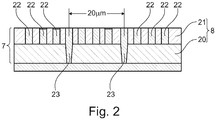
- FIG. 2 illustrates a redistribution structure 7 of an interposer-type component carrier 1 according to an exemplary embodiment of the invention.
- the redistribution structure 7 comprises microvias 23 with a high density, for example with a distance of 20 ⁇ m between adjacent microvias 23.
- the redistribution structure 7 with such a high I/O density can be manufactured by a so called via-in-trench (ViT) technology, in particular by a dual damascene process.
- the dual damascene process can have the following steps:
- the vias 23 are formed after the trenches 22, i.e. the vias 23 are arranged underneath the trenches 22.
- the embodiment can be modified in that the vias 23 are formed before the trenches 22, i.e. the trenches 22 are arranged underneath the vias 23, for example by interchanging the inter-level dielectric (ILD) and the inter-metal dielectric (IMD).
- ILD inter-level dielectric
- IMD inter-metal dielectric
- the redistribution structure 7 comprises the trenches 22 and the vias 23.
- the inter-level dielectric (ILD) 20 and the inter-metal dielectric (IMD) 21 are contiguous, amongst others by the interconnected vias 23 and trenches 22, so that the inter-level dielectric (ILD) 20 and the inter-metal dielectric (IMD) 21 form together the only one electrically insulating layer structure 8 of the redistribution structure 7 in the meaning of the present invention.
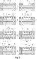
- Figure 3 illustrates a method of manufacturing an interposer-type component carrier 1 according to an exemplary embodiment of the invention.
- a stack is formed comprising electrically conductive layer structures 2 and an electrically insulating layer structure 3.
- the stack can be formed by conventional PCB processes.
- the stack can be coreless stack, and the stack can be symmetrically or asymmetrically built up.
- electrically conductive layer structures 2 are schematically depicted in Figure 3 as straight interconnected lines, the present invention is not limited thereto.
- the electrically conductive layer structures 2 can assume any (partially) patterned conductive layer shapes.
- a cavity 4 is formed in an upper portion of the stack.
- the cavity 4 can be formed by mechanical drilling, etching and/or laser drilling.
- the electrically conductive layer structures 2 can first be roughened or blackened by an UV laser, wherein the roughened or blackened parts are subsequently removed by a CO 2 laser. Parts of the electrically conductive layer structures 2 and/or the electrically insulating layer structure 3 are thus removed to form the cavity 4.
- a gap between a cavity bottom and a component can be filled with an extra dielectric material using e.g. inkjet or dispenser.
- a dielectric layer of a next build-up layer can be used to fill the gap.
- the bottom of the cavity 4 can be covered with a copper layer to support the thermal management for a component that is placed and embedded in the cavity 4.
- This copper layer can be exposed during forming the cavity 4.
- This copper layer can be provided in addition or as an alternative to the above described thermally highly conductive material, which is in particular a copper block.
- an active component 5 is embedded in the cavity 4, wherein the active component 5 has terminals 6 facing upwards.
- the active component 5 can be a semiconductor chip, in particular at least one of a memory chip, a controller chip, a microprocessor chip, a transmitter chip, and a receiver chip.
- a block of a thermally highly conductive material in particular a copper block, can optionally be placed in the cavity 4 below the active component 5.
- an electrically insulating material is filled in the cavity 4 to form the electrically insulating layer structure 8 above the component 5.
- the electrically insulating material can optionally be filled at side surfaces of the component 5 and on the remaining upper surface of the stack.
- the electrically insulating layer structure 8 can comprise a PID (photoimageable dielectric) material, or alternatively a liquid or powdery material or a dry film.
- vias 23 corresponding to the terminals 6 of the active component 5 are formed in the electrically insulating layer structure 8.
- trenches can also be formed in the electrically insulating layer structure 8.
- the only electrically insulating layer structure of the redistribution structure 8 is patterned, which can be done by a lithographic process or another photo process, plasma etching, imprinting, laser grooving or dry etching.
- photovias 23 have benefits of a high registration, lower costs and less thermal damage of the component.
- a step S6 the vias 23 and optionally the trenches are filled or plated by an electrically conductive material such as copper to form a preform of an upper electrically conductive layer structure 13.
- an electrically conductive material such as copper to form a preform of an upper electrically conductive layer structure 13.
- a thin copper seed layer can optionally be deposited by physical vapor deposition (PVD).
- the upper electrically conductive layer structure 13 is patterned or structured by conventional lithography and etching processes.
- an electrically insulating solder resist 12 is applied to a part of an upper main surface, here on the upper electrically conductive layer structure 13, of the thus manufactured component carrier 1.
- a further cavity can be formed in step S2, in which a further active component is embedded in step S3.
- the active component 5 can interactively be connected with the further active component, more particularly through the at least one electrically conductive layer structure 2 or through the upper electrically conductive layer structure 13 of the redistribution structure 7.
- the active component 5 and the further active component can have different heights. Accordingly, different depths of the cavity 4 and the further cavity can readily be created in step S2.
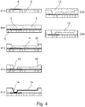
- Figure 4 illustrates a method of manufacturing a redistribution structure 7 of an interposer-type component carrier 1 according to another exemplary embodiment of the invention.
- Step S10 shows the initial situation where the component 5 having the terminal 6 faced upwards is placed in the cavity 4 of the component carrier 1 (see Figure 1 ).
- an electrically insulating layer structure 8 is formed in the cavity 4 above the component 5 (see also Figure 1 ).
- the electrically insulating layer structure 8 can comprise a PID (photoimageable dielectric) material, or a liquid or powdery material or a dry film.
- a lithography or another photo process, plasma etching, imprinting, laser grooving or dry etching is carried out to form a trench 22 in the electrically insulating layer structure 8.
- a lithography or another photo process, plasma etching, imprinting, laser grooving or dry etching is carried out to form a via 23 in the electrically insulating layer structure 8, wherein the via 23 is underneath the trench 22.
- the trench 22 can be formed underneath the via 23.
- a seed layer 14 is applied on the electrically insulating layer structure 8, i.e. in the trench 22 and the via 23, for example by physical vapor deposition (PVD).
- PVD physical vapor deposition
- a metal such as copper is applied to the seed layer 14 in the trenches 22 and the vias 23, for example by copper electroplating.
- a step S16 an excess of the copper can be removed, for example by a chemical mechanical polishing process (CMP).
- CMP chemical mechanical polishing process
- a finish (not shown), for example an electrically insulating solder resist, can be applied to the polished metal surface.
- the methods shown in Figures 3 and 4 can be carried out in that only known good active components 5 are embedded in cavities 4 of a stack.
- the meaning of the term "known good” can include previously successfully tested active components, cavities and/or stacks.
- a step of testing the active component 5 can be carried out before embedding the same in the cavity 4.
- a step of testing the cavity 4 can optionally be carried out before embedding the active component 5 therein.
- a step of testing the stack can optionally be carried out before forming the cavity 4 or before embedding the active component 5 therein.
Landscapes
- Physics & Mathematics (AREA)
- Engineering & Computer Science (AREA)
- Microelectronics & Electronic Packaging (AREA)
- General Physics & Mathematics (AREA)
- Optics & Photonics (AREA)
- Production Of Multi-Layered Print Wiring Board (AREA)
- Geometry (AREA)
Abstract
Description
- The invention relates to an interposer-type component carrier and to a method of manufacturing the same.
- A conventional interposer-type component carrier comprises a stack having at least one electrically conductive layer structure and at least one electrically insulating layer structure, and an active component which is surface mounted with its contacts facing downwards on the stack. The term "facing downwards" means that the component is embedded in the component carrier with the contacts of the component being arranged at the bottom main surface of the component. This configuration usually requires a plurality of fan out layers.
- Once the chip is embedded, many inter-metallic interfaces are built up thereon so that the component carrier can suffer on parasitic influences such as parasitic inductivities or parasitic capacities which may form an undesired resonant circuit, wherein disturbing voltage oscillations can damage semiconductor components and worsen electromagnetic compatibility and signal transmission properties. This can also lead to a loss or a decrease in signal and power integrity. In addition, the component is often a semiconductor chip which can be damaged during manufacturing the component carrier. The manufacturing method as described creates or poses a high risk for yield loss.
- There may be a need of an interposer-type component carrier and a method of manufacturing the same, by which the yield is improved and parasitic influences are reduced, while a sufficient fan-out is provided. This need may be met by the interposer-type component carrier and the method of manufacturing the same set forth in the independent claims.
- According to an exemplary embodiment of the invention, an interposer-type component carrier is provided, the interposer-type component carrier comprising a stack having at least one electrically conductive layer structure and at least one electrically insulating layer structure; a cavity formed in an upper portion of the stack; an active component embedded in the cavity and having at least one terminal facing upwards; and a redistribution structure having only electrically insulating layer structure above the component.
- According to an exemplary embodiment of the invention, a method of manufacturing an interposer-type component carrier is provided, the method comprising providing a stack comprising at least one electrically conductive layer structure and at least one electrically insulating layer structure; forming a cavity in an upper portion of the stack; embedding an active component in the cavity so that at least one terminal of the component faces upwards; and forming a redistribution structure having only one electrically insulating layer structure above the component.
- According to the invention, the active component can be embedded in the cavity at a very late stage of the manufacturing process of the interposer-type component carrier so that damages of the active component during the remainder of the manufacturing process are not likely. Before the active component is embedded, the stack is nearly completed and optionally tested. Since the active component is embedded as late as possible because only the one electrically insulating layer structure is to be arranged above the component, a high yield can be obtained and material costs can be saved.
- In the present invention, only one redistribution structure or redistribution layer is required so that the number of inter-metallic interfaces above the active component and thus parasitic influences can be reduced. A length of line connections between active component and a main surface of the interposer-type component carrier, where other components can be connected, can be shortened.
- In the context of the present application, the term "only one electrically insulating layer structure above the component" can either mean exactly one or several individual but contiguous layers (of same or different materials) consecutively applied atop each other. The only one electrically insulating layer structure above the component can have a plurality of internal routing layers which are formed by several (thin) layers of an electrically conductive material, wherein these routing layers can have different densities.
- In addition, the present invention enables a simple creation of the required cavity so that different cavity depths are possible.
- It is possible that the active component has a plurality of terminals, wherein all terminals thereof are facing upwards.
- In the following, further exemplary embodiments of the present invention will be explained.
- According to an exemplary embodiment of the interposer-type component carrier, the terminal is an electrically conductive pad and the redistribution structure comprises an electrically conductive connection of the pad up to an exterior surface of the component carrier.
- According to an exemplary embodiment of the interposer-type component carrier, the terminal is an optical terminal and the redistribution structure comprises at least one lightguide extending up to an exterior surface of the component carrier. The lightguide can be a glass fiber which is embedded in the redistribution structure, or the lightguide can be part of the only one electrically insulating layer structure above the component. The lightguide can by formed by altering an index of refraction in parts of the only one electrically insulating layer structure above the component.
- According to an exemplary embodiment of the interposer-type component carrier, the active component is a semiconductor chip, in particular at least one of a memory chip, a controller chip, a microprocessor chip, a transmitter chip, and a receiver chip.
- According to an exemplary embodiment of the interposer-type component carrier, the interposer-type component carrier comprises a layer or block of thermally highly conductive material, in particular a copper layer or a copper block, in the cavity below the active component. The layer or the block of thermally highly conductive material promotes heat dissipation from the active component.
- According to an exemplary embodiment of the interposer-type component carrier, the interposer-type component carrier comprises a further cavity in which a further active component is embedded, wherein in particular the active component is interactively connected with the further active component, more particularly through the at least one electrically conductive layer structure.
- According to an exemplary embodiment of the interposer-type component carrier, the active component and the further active component have different heights. The different heights can readily be created when forming the cavities in the stack.
- According to an exemplary embodiment of the interposer-type component carrier, the only electrically insulating layer structure of the redistribution structure comprises or consists of a photoimageable dielectric (PID). The PID enables very fine, high-density fan-out layers, for example by a dual damascene process. The PID further reduces thermal and mechanical stresses to the stack and the active component.
- According to an exemplary embodiment of the interposer-type component carrier, the only electrically insulating layer structure of the redistribution structure is liquid, powdery or a dry film.
- According to an exemplary embodiment of the interposer-type component carrier, the only electrically insulating layer structure of the redistribution structure is patterned by a lithographic process or another photo process or plasma etching, imprinting, laser grooving or dry etching.
- According to an exemplary embodiment of the interposer-type component carrier, the interposer-type component carrier comprises an electrically insulating solder resist on a part of an upper main surface of the component carrier.
- According to an exemplary embodiment of the interposer-type component carrier, at least one of the active component, the cavities and the stack are known good. The meaning of the term "known good" can include previously successfully tested active components, cavities and/or stacks, i.e. at least one of the active component, the cavity and the stack successfully passed a previous test. Thereby, a high yield can be obtained and material costs can be saved. However, a test is not always obligatory if the active component, the cavity and/or the stack are known to be good for other reasons. For example, the active component, the cavity and/or the stack can be known to be good when their manufacturing processes have a certain (quality) standard or their reject rate in the manufacturing process is generally lower than a certain limit.
- According to an exemplary embodiment of the invention, the interposer-type component carrier comprises at least one of the following features: the component carrier comprises at least one component being surface mounted on and/or embedded in the component carrier, wherein the at least one component is in particular selected from a group consisting of an electronic component, an electrically non-conductive and/or electrically conductive inlay, a heat transfer unit, a light guiding element, an energy harvesting unit, an active electronic component, a passive electronic component, an electronic chip, a storage device, a filter, an integrated circuit, a signal processing component, a power management component, an optoelectronic interface element, a voltage converter, a cryptographic component, a transmitter and/or receiver, an electromechanical transducer, an actuator, a microelectromechanical system, a microprocessor, a capacitor, a resistor, an inductance, an accumulator, a switch, a camera, an antenna, a magnetic element, a further component carrier, and a logic chip; wherein at least one of the electrically conductive layer structures of the component carrier comprises at least one of the group consisting of copper, aluminum, nickel, silver, gold, palladium, and tungsten, any of the mentioned materials being optionally coated with supra-conductive material such as graphene; wherein the electrically insulating layer structure comprises at least one of the group consisting of resin, in particular reinforced or non-reinforced resin, for instance epoxy resin or bismaleimide-triazine resin, FR-4, FR-5, cyanate ester, polyphenylene derivate, glass, prepreg material, polyimide, polyamide, liquid crystal polymer, epoxy-based build-up material, polytetrafluoroethylene, a ceramic, and a metal oxide; wherein the component carrier is shaped as a plate; wherein the component carrier is configured as one of the group consisting of a printed circuit board, a substrate, and an interposer; wherein the component carrier is configured as a laminate-type component carrier.
- According to an exemplary embodiment of the method, the terminal is an electrically conductive pad and the redistribution structure comprises an electrically conductive connection of the pad up to an exterior surface of the component carrier.
- According to an exemplary embodiment of the method, the terminal is an optical terminal and the redistribution structure comprises at least one lightguide extending up to an exterior surface of the component carrier.
- According to an exemplary embodiment of the method, the active component is a semiconductor chip, in particular at least one of a memory chip, a controller chip, a microprocessor chip, a transmitter chip, and a receiver chip.
- According to an exemplary embodiment, the method comprises applying a layer or inserting a block of thermally highly conductive material, in particular a copper layer or a copper block, in the cavity before embedding the active component in the cavity.
- According to an exemplary embodiment, the method comprises embedding a further active component in a further cavity of the interposer-type component carrier, wherein in particular the active component is interactively connected with the further active component, more particularly through the at least one electrically conductive layer structure.
- According to an exemplary embodiment of the method, the active component and the further active component have different heights.
- According to an exemplary embodiment of the method, the only electrically insulating layer structure of the redistribution structure comprises or consists of a photoimageable dielectric.
- According to an exemplary embodiment of the method, the only electrically insulating layer structure of the redistribution structure is liquid, powdery or a dry film.
- According to an exemplary embodiment of the method, the only electrically insulating layer structure of the redistribution structure is patterned by a lithographic process or another photo process,, plasma etching, imprinting, laser grooving or dry etching.
- According to an exemplary embodiment, the method comprises applying an electrically insulating solder resist on a part of an upper main surface of the component carrier.
- According to an exemplary embodiment of the method, only known good active components are embedded in known good cavities of known good stack.
- In the context of the present application, the term "component carrier" may particularly denote any support structure which is capable of accommodating one or more components thereon and/or therein for providing mechanical support and/or electrical connectivity. In other words, a component carrier may be configured as a mechanical and/or electronic carrier for components. In particular, a component carrier may be one of a printed circuit board, an organic interposer, and an IC (integrated circuit) substrate. A component carrier may also be a hybrid board combining different ones of the above mentioned types of component carriers.
- In an embodiment, the component carrier comprises a stack of at least one electrically insulating layer structure and at least one electrically conductive layer structure. For example, the component carrier may be a laminate of the mentioned electrically insulating layer structure(s) and electrically conductive layer structure(s), in particular formed by applying mechanical pressure and/or thermal energy. The mentioned stack may provide a plate-shaped component carrier capable of providing a large mounting surface for further components and being nevertheless very thin and compact. The term "layer structure" may particularly denote a continuous layer, a patterned layer or a plurality of nonconsecutive islands within a common plane.
- In an embodiment, the component carrier is shaped as a plate. This contributes to the compact design, wherein the component carrier nevertheless provides a large basis for mounting components thereon. Furthermore, in particular a naked die as example for an embedded electronic component, can be conveniently embedded, thanks to its small thickness, into a thin plate such as a printed circuit board.
- In an embodiment, the component carrier is configured as one of the group consisting of a printed circuit board, a substrate (in particular an IC substrate), and an interposer.
- In the context of the present application, the term "printed circuit board" (PCB) may particularly denote a plate-shaped component carrier which is formed by laminating several electrically conductive layer structures with several electrically insulating layer structures, for instance by applying pressure and/or by the supply of thermal energy. As preferred materials for PCB technology, the electrically conductive layer structures are made of copper, whereas the electrically insulating layer structures may comprise resin and/or glass fibers, so-called prepreg or FR4 material. The various electrically conductive layer structures may be connected to one another in a desired way by forming through-holes through the laminate, for instance by laser drilling or mechanical drilling, and by filling them with electrically conductive material (in particular copper), thereby forming vias as through-hole connections. Apart from one or more components which may be embedded in a printed circuit board, a printed circuit board is usually configured for accommodating one or more components on one or both opposing surfaces of the plate-shaped printed circuit board. They may be connected to the respective main surface by soldering. A dielectric part of a PCB may be composed of resin with reinforcing fibers (such as glass fibers).
- In the context of the present application, the term "substrate" may particularly denote a small component carrier having substantially the same size as a component (in particular an electronic component) to be mounted thereon. More specifically, a substrate can be understood as a carrier for electrical connections or electrical networks as well as component carrier comparable to a printed circuit board (PCB), however with a considerably higher density of laterally and/or vertically arranged connections. Lateral connections are for example conductive paths, whereas vertical connections may be for example drill holes. These lateral and/or vertical connections are arranged within the substrate and can be used to provide electrical and/or mechanical connections of housed components or unhoused components (such as bare dies), particularly of IC chips, with a printed circuit board or intermediate printed circuit board. Thus, the term "substrate" also includes "IC substrates". A dielectric part of a substrate may be composed of resin with reinforcing particles (such as reinforcing spheres, in particular glass spheres).
- The substrate or interposer may comprise or consist of at least a layer of glass, silicon (Si) or a photoimageable or dry-etchable organic material like epoxy-based build-up material (such as epoxy-based build-up film) or polymer compounds like polyimide, polybenzoxazole, or benzocyclobutene.
- In an embodiment, the at least one electrically insulating layer structure comprises at least one of the group consisting of resin (such as reinforced or non-reinforced resins, for instance epoxy resin or bismaleimide-triazine resin), cyanate ester, polyphenylene derivate, glass (in particular glass fibers, multilayer glass, glass-like materials), prepreg material (such as FR-4 or FR-5), polyimide, polyamide, liquid crystal polymer (LCP), epoxy-based build-up film, polytetrafluoroethylene (teflon), a ceramic, and a metal oxide. Reinforcing materials such as webs, fibers or spheres, for example made of glass (multilayer glass) may be used as well. Although prepreg particularly FR4 are usually preferred for rigid PCBs, other materials in particular epoxy-based build-up film for substrates may be used as well. For high frequency applications, highfrequency materials such as polytetrafluoroethylene, liquid crystal polymer and/or cyanate ester resins, low temperature cofired ceramics (LTCC) or other low, very low or ultra-low DK materials may be implemented in the component carrier as electrically insulating layer structure.
- In an embodiment, the at least one electrically conductive layer structure comprises at least one of the group consisting of copper, aluminum, nickel, silver, gold, palladium, and tungsten. Although copper is usually preferred, other materials or coated versions thereof are possible as well, in particular coated with supra-conductive material such as graphene.
- The at least one component can be selected from a group consisting of an electrically non-conductive inlay, an electrically conductive inlay (such as a metal inlay, preferably comprising copper or aluminum), a heat transfer unit (for example a heat pipe), a light guiding element (for example an optical waveguide or a light conductor connection), an electronic component, or combinations thereof. For example, the component can be an active electronic component, a passive electronic component, an electronic chip, a storage device (for instance a DRAM or another data memory), a filter, an integrated circuit, a signal processing component, a power management component, an optoelectronic interface element, a light emitting diode, a photocoupler, a voltage converter (for example a DC/DC converter or an AC/DC converter), a cryptographic component, a transmitter and/or receiver, an electromechanical transducer, a sensor, an actuator, a microelectromechanical system (MEMS), a microprocessor, a capacitor, a resistor, an inductance, a battery, a switch, a camera, an antenna, a logic chip, and an energy harvesting unit. However, other components may be embedded in the component carrier. For example, a magnetic element can be used as a component. Such a magnetic element may be a permanent magnetic element (such as a ferromagnetic element, an antiferromagnetic element, a multiferroic element or a ferrimagnetic element, for instance a ferrite core) or may be a paramagnetic element. However, the component may also be a substrate, an interposer or a further component carrier, for example in a board-in-board configuration. The component may be surface mounted on the component carrier and/or may be embedded in an interior thereof. Moreover, also other components, in particular those which generate and emit electromagnetic radiation and/or are sensitive with regard to electromagnetic radiation propagating from an environment, may be used as component.
- In an embodiment, the component carrier is a laminate-type component carrier. In such an embodiment, the component carrier is a compound of multiple layer structures which are stacked and connected together by applying a pressing force and/or heat.
- The aspects defined above and further aspects of the invention are apparent from the examples of embodiment to be described hereinafter and are explained with reference to these examples of embodiment.
-
-
Figure 1 illustrates a cross-sectional view of an interposer-type component carrier according to an exemplary embodiment of the invention. -
Figure 2 illustrates a redistribution structure of an interposer-type component carrier according to an exemplary embodiment of the invention. -
Figure 3 illustrates a method of manufacturing an interposer-type component carrier according to an exemplary embodiment of the invention. -
Figure 4 illustrates a method of manufacturing a redistribution structure of an interposer-type component carrier according to an exemplary embodiment of the invention. - The illustrations in the drawings are schematic. In different drawings, similar or identical elements are provided with the same reference signs.
-
Figure 1 illustrates a cross-sectional view of an interposer-type component carrier 1 according to an exemplary embodiment of the invention. The interposer-type component carrier 1 can be shaped as a plate. - The interposer-type component carrier comprises a stack having electrically
conductive layer structures 2 and an electrically insulatinglayer structure 3. - The electrically
conductive layer structures 2 of the component carrier can comprise at least one of the group consisting of copper, aluminum, nickel, silver, gold, palladium, and tungsten, any of the mentioned materials being optionally coated with supra-conductive material such as graphene. - The electrically insulating
layer structure 3 can comprise at least one of the group consisting of resin, in particular reinforced or non-reinforced resin, for instance epoxy resin or bismaleimide-triazine resin, FR-4, FR-5, cyanate ester, polyphenylene derivate, glass, prepreg material, polyimide, polyamide, liquid crystal polymer, epoxy-based build-up film, polytetrafluoroethylene, a ceramic, and a metal oxide. - A
cavity 4 is formed in an upper portion of the stack. - An
active component 5 is embedded in thecavity 4 and hasterminals 6 facing upwards. Theactive component 5 can be a semiconductor chip, in particular at least one of a memory chip, a controller chip, a microprocessor chip, a transmitter chip, and a receiver chip. - The interposer-type component carrier 1 comprises a
redistribution structure 7. Theredistribution structure 7 is formed as a redistribution layer which is connected to theterminals 6 of theactive component 5 having a smaller density and comprises an upper electricallyconductive layer structure 13 having a higher density. The upper electricallyconductive layer structure 13 can form a first level interconnection (i.e. a die connection and a fan out). -
Solder balls 11 at the bottom main surface of the interposer-type component carrier 1 are connected to a respective electricallyconductive layer structure 2 and form end terminals of the interposer-type component carrier 1 having the smaller density. The upper electricallyconductive layer structure 13 forms terminals or solder pads with the larger density, which can be connected toterminals 15 of other dies orother components 16. - The
redistribution structure 7 comprises only one electrically insulatinglayer structure 8 above thecomponent 5. The only electrically insulatinglayer structure 8 of theredistribution structure 7 comprises or consists of a photoimageable dielectric. - The only electrically insulating
layer structure 8 of theredistribution structure 7 can be obtained by a patterning process such as a lithographic process or another photo process, plasma etching, imprinting, laser grooving or dry etching. - The only electrically insulating
layer structure 8 of theredistribution structure 7 can alternatively be liquid, powdery or a dry film. - In the embodiment, the
terminals 6 are electrically conductive pads and theredistribution structure 7 comprises an electrically conductive connection of thepads 6 up to an exterior surface of the component carrier 1. In a modified embodiment, theterminal 6 of thecomponent 5 can be an optical terminal and theredistribution structure 7 can comprise at least one lightguide extending up to an exterior surface of the component carrier 1. - The interposer-type component carrier 1 further comprises a
further cavity 9 in which a furtheractive component 10 is embedded, wherein in particular theactive component 5 is interactively connected with the furtheractive component 10, more particularly through the at least one electricallyconductive layer structure 2 and/or the upper electricallyconductive layer structure 13. Theactive component 5 and the furtheractive component 10 can have different heights. The depths of thecavities active component 5 and the furtheractive component 10. Upper main surfaces of theactive component 5 and the furtheractive component 10 can be aligned to the same level. - The interposer-type component carrier 1 comprises an electrically insulating solder resist 12 on a part of an upper main surface of the component carrier 1.
- A finish 17, for example an electrically insulating solder resist, is applied to the bottom main surface of the component carrier 1.
- In order to enhance the yield of manufacturing of the interposer-type component carrier 1, only known good active components are embedded in known good cavities of known good stack. The meaning of the term "known-good" can include previously successfully tested active components, cavities and/or stacks. That means, at least one of the
active components cavities - In a modified embodiment, the interposer-type component carrier 1 can comprise a block of thermally highly conductive material, in particular a copper block, in the
cavity 4 below theactive component 5 so that the heat dissipation from theactive component 5 is promoted. - The interposer-type component carrier 1 can further comprise an additional component (not shown) which is selected from a group consisting of an electronic component, an electrically non-conductive and/or electrically conductive inlay, a heat transfer unit, a light guiding element, an energy harvesting unit, an active electronic component, a passive electronic component, an electronic chip, a storage device, a filter, an integrated circuit, a signal processing component, a power management component, an optoelectronic interface element, a voltage converter, a cryptographic component, a transmitter and/or receiver, an electromechanical transducer, an actuator, a microelectromechanical system, a microprocessor, a capacitor, a resistor, an inductance, an accumulator, a switch, a camera, an antenna, a magnetic element, a further component carrier, and a logic chip.
-
Figure 2 illustrates aredistribution structure 7 of an interposer-type component carrier 1 according to an exemplary embodiment of the invention. In the embodiment, theredistribution structure 7 comprisesmicrovias 23 with a high density, for example with a distance of 20 µm betweenadjacent microvias 23. Theredistribution structure 7 with such a high I/O density can be manufactured by a so called via-in-trench (ViT) technology, in particular by a dual damascene process. In an embodiment, the dual damascene process can have the following steps: - In a first step, an inter-level dielectric (ILD) 20 can be applied to the stack.
- In a second step, an etch stop layer (not shown) is applied to the
inter-level dielectric 20. - In a third step, an inter-metal dielectric (IMD) 21 is applied to the etch stop layer.
- In a fourth step, a photoresist is applied to the
inter-metal dielectric 21 and structured by a lithography process or another photo process, plasma etching, imprinting, laser grooving or dry etching. - In a fifth step, the
inter-metal dielectric 21 is etched to formtrenches 22. - in a sixth step, the photoresist is removed or stripped.
- In a seventh step, another photoresist is applied to the
inter-metal dielectric 21 and the etch stop layer, and this photoresist is structured by a lithography process or another photo process, plasma etching, imprinting, laser grooving or dry etching. - In an eighth step, the etch stop layer and the
inter-level dielectric 20 are etched to form vias (microvias) 23. - In a ninth step, the other photoresist is removed or stripped. In addition, a cleaning step can be performed, and a hydrophobic coating (e.g. for Cu Migration) and/or a diffusion barrier, for example a tantal-based layer (Ta), can be applied to the
trenches 22 and thevias 23. - In a tenth step, a metal is filled in the
trenches 22 and thevias 23, for example by copper electroplating. Before that, a copper seed layer can optionally be deposited by physical vapor deposition (PVD). After the copper electroplating step, an excess of the copper can be removed, for example by a chemical mechanical polishing process (CMP). At the end, a finish (not shown) can be applied to theinter-metal dielectric 21 and thetrenches 22. - In this embodiment of the dual damascene process, the
vias 23 are formed after thetrenches 22, i.e. thevias 23 are arranged underneath thetrenches 22. The embodiment can be modified in that thevias 23 are formed before thetrenches 22, i.e. thetrenches 22 are arranged underneath thevias 23, for example by interchanging the inter-level dielectric (ILD) and the inter-metal dielectric (IMD). - In any case, the
redistribution structure 7 comprises thetrenches 22 and thevias 23. - In the embodiment of the dual damascene process, the inter-level dielectric (ILD) 20 and the inter-metal dielectric (IMD) 21 are contiguous, amongst others by the
interconnected vias 23 andtrenches 22, so that the inter-level dielectric (ILD) 20 and the inter-metal dielectric (IMD) 21 form together the only one electrically insulatinglayer structure 8 of theredistribution structure 7 in the meaning of the present invention. -
Figure 3 illustrates a method of manufacturing an interposer-type component carrier 1 according to an exemplary embodiment of the invention. - In a step S1, a stack is formed comprising electrically
conductive layer structures 2 and an electrically insulatinglayer structure 3. The stack can be formed by conventional PCB processes. The stack can be coreless stack, and the stack can be symmetrically or asymmetrically built up. - It is to be noted that, even though the electrically
conductive layer structures 2 are schematically depicted inFigure 3 as straight interconnected lines, the present invention is not limited thereto. The electricallyconductive layer structures 2 can assume any (partially) patterned conductive layer shapes. - In a step S2, a
cavity 4 is formed in an upper portion of the stack. For example, thecavity 4 can be formed by mechanical drilling, etching and/or laser drilling. For example, the electricallyconductive layer structures 2 can first be roughened or blackened by an UV laser, wherein the roughened or blackened parts are subsequently removed by a CO2 laser. Parts of the electricallyconductive layer structures 2 and/or the electrically insulatinglayer structure 3 are thus removed to form thecavity 4. In addition, it is possible to refill a part of thecavity 4 by an electrically insulating material. For example, a gap between a cavity bottom and a component can be filled with an extra dielectric material using e.g. inkjet or dispenser. Alternatively, a dielectric layer of a next build-up layer can be used to fill the gap. - Optionally (not shown in drawings), the bottom of the
cavity 4 can be covered with a copper layer to support the thermal management for a component that is placed and embedded in thecavity 4. This copper layer can be exposed during forming thecavity 4. This copper layer can be provided in addition or as an alternative to the above described thermally highly conductive material, which is in particular a copper block. - In a step S3, an
active component 5 is embedded in thecavity 4, wherein theactive component 5 hasterminals 6 facing upwards. Theactive component 5 can be a semiconductor chip, in particular at least one of a memory chip, a controller chip, a microprocessor chip, a transmitter chip, and a receiver chip. - Before embedding the
active component 5 in thecavity 4, a block of a thermally highly conductive material, in particular a copper block, can optionally be placed in thecavity 4 below theactive component 5. - In a step S4, an electrically insulating material is filled in the
cavity 4 to form the electrically insulatinglayer structure 8 above thecomponent 5. The electrically insulating material can optionally be filled at side surfaces of thecomponent 5 and on the remaining upper surface of the stack. The electrically insulatinglayer structure 8 can comprise a PID (photoimageable dielectric) material, or alternatively a liquid or powdery material or a dry film. The - In a step S5, vias 23 corresponding to the
terminals 6 of theactive component 5 are formed in the electrically insulatinglayer structure 8. Optionally, trenches (not shown) can also be formed in the electrically insulatinglayer structure 8. Thereby, the only electrically insulating layer structure of theredistribution structure 8 is patterned, which can be done by a lithographic process or another photo process, plasma etching, imprinting, laser grooving or dry etching. In particular if another component is connected to the component carrier 1 by a flip-chip connection, photovias 23 have benefits of a high registration, lower costs and less thermal damage of the component. - In a step S6, the
vias 23 and optionally the trenches are filled or plated by an electrically conductive material such as copper to form a preform of an upper electricallyconductive layer structure 13. Before the electroplating process, a thin copper seed layer can optionally be deposited by physical vapor deposition (PVD). - In a step S7, the upper electrically
conductive layer structure 13 is patterned or structured by conventional lithography and etching processes. - In a step S8, an electrically insulating solder resist 12 is applied to a part of an upper main surface, here on the upper electrically
conductive layer structure 13, of the thus manufactured component carrier 1. - Alternatively, a dual damascene process similar to
Figure 2 can be carried out in the steps S4 to S7 ofFigure 3 to form theredistribution structure 7. - In a modified embodiment, a further cavity can be formed in step S2, in which a further active component is embedded in step S3. The
active component 5 can interactively be connected with the further active component, more particularly through the at least one electricallyconductive layer structure 2 or through the upper electricallyconductive layer structure 13 of theredistribution structure 7. Furthermore, theactive component 5 and the further active component can have different heights. Accordingly, different depths of thecavity 4 and the further cavity can readily be created in step S2. -
Figure 4 illustrates a method of manufacturing aredistribution structure 7 of an interposer-type component carrier 1 according to another exemplary embodiment of the invention. - Step S10 shows the initial situation where the
component 5 having theterminal 6 faced upwards is placed in thecavity 4 of the component carrier 1 (seeFigure 1 ). - In a step S11, an electrically insulating
layer structure 8 is formed in thecavity 4 above the component 5 (see alsoFigure 1 ). The electrically insulatinglayer structure 8 can comprise a PID (photoimageable dielectric) material, or a liquid or powdery material or a dry film. - In a step S12, a lithography or another photo process, plasma etching, imprinting, laser grooving or dry etching is carried out to form a
trench 22 in the electrically insulatinglayer structure 8. - In a step S13, a lithography or another photo process, plasma etching, imprinting, laser grooving or dry etching is carried out to form a via 23 in the electrically insulating
layer structure 8, wherein the via 23 is underneath thetrench 22. Alternatively, thetrench 22 can be formed underneath the via 23. - In a step S14, a
seed layer 14 is applied on the electrically insulatinglayer structure 8, i.e. in thetrench 22 and the via 23, for example by physical vapor deposition (PVD). - In a step S15, a metal such as copper is applied to the
seed layer 14 in thetrenches 22 and thevias 23, for example by copper electroplating. - In a step S16, an excess of the copper can be removed, for example by a chemical mechanical polishing process (CMP). Eventually, a finish (not shown), for example an electrically insulating solder resist, can be applied to the polished metal surface.
- The methods shown in
Figures 3 and4 can be carried out in that only known goodactive components 5 are embedded incavities 4 of a stack. The meaning of the term "known good" can include previously successfully tested active components, cavities and/or stacks. Thus, a step of testing theactive component 5 can be carried out before embedding the same in thecavity 4. In addition, a step of testing thecavity 4 can optionally be carried out before embedding theactive component 5 therein. In addition, a step of testing the stack can optionally be carried out before forming thecavity 4 or before embedding theactive component 5 therein. - It should be noted that the term "comprising" does not exclude other elements or steps and the "a" or "an" does not exclude a plurality. Also elements described in association with different embodiments may be combined.
- It should also be noted that reference signs in the claims shall not be construed as limiting the scope of the claims.
- Implementation of the invention is not limited to the preferred embodiments shown in the figures and described above. Instead, a multiplicity of variants are possible which use the solutions shown and the principle according to the invention even in the case of fundamentally different embodiments.
Claims (15)
- An interposer-type component carrier (1), comprising:a stack comprising at least one electrically conductive layer structure (2) and at least one electrically insulating layer structure (3);a cavity (4) formed in an upper portion of the stack;an active component (5) embedded in the cavity (4) and having at least one terminal (6) facing upwards;a redistribution structure (7) having only one electrically insulating layer structure (8) above the component (5).
- The interposer-type component carrier (1) according to claim 1,
wherein the terminal (6) is an electrically conductive pad and the redistribution structure (7) comprises an electrically conductive connection of the pad up to an exterior surface of the component carrier (1). - The interposer-type component carrier (1) according to claim 1 or claim 2,
wherein the terminal (6) is an optical terminal and the redistribution structure (7) comprises at least one lightguide extending up to an exterior surface of the component carrier (1). - The interposer-type component carrier (1) according to any one of the preceding claims,
wherein the active component (5) is a semiconductor chip, in particular at least one of a memory chip, a controller chip, a microprocessor chip, a transmitter chip, and a receiver chip. - The interposer-type component carrier (1) according to any one of the preceding claims,
further comprising a layer or block of thermally highly conductive material, in particular a copper layer or a copper block, in the cavity (4) below the active component (5). - The interposer-type component carrier (1) according to any one of the preceding claims,
comprising a further cavity (9) in which a further active component (10) is embedded, wherein in particular the active component (5) is interactively connected with the further active component (10), more particularly through the at least one electrically conductive layer structure (2). - The interposer-type component carrier (1) according to claim 6,
wherein the active component (5) and the further active component (10) have different heights. - The interposer-type component carrier (1) according to any one of the preceding claims,
wherein the only electrically insulating layer structure (8) of the redistribution structure (7) comprises or consists of a photoimageable dielectric. - The interposer-type component carrier (1) according to any one of the preceding claims,
wherein the only electrically insulating layer structure (8) of the redistribution structure (7) is liquid, powdery or a dry film. - The interposer-type component carrier (1) according to any one of the preceding claims,
comprising an electrically insulating solder resist (12) on a part of an upper main surface of the component carrier (1). - The interposer-type component carrier (1) according to any one of the preceding claims,
comprising at least one of the following features:the component carrier (1) comprises at least one component being surface mounted on and/or embedded in the component carrier (1), wherein the at least one component is in particular selected from a group consisting of an electronic component, an electrically non-conductive and/or electrically conductive inlay, a heat transfer unit, a light guiding element, an energy harvesting unit, an active electronic component, a passive electronic component, an electronic chip, a storage device, a filter, an integrated circuit, a signal processing component, a power management component, an optoelectronic interface element, a voltage converter, a cryptographic component, a transmitter and/or receiver, an electromechanical transducer, an actuator, a microelectromechanical system, a microprocessor, a capacitor, a resistor, an inductance, an accumulator, a switch, a camera, an antenna, a magnetic element, a further component carrier (1), and a logic chip;wherein the at least one electrically conductive layer structure (2) of the component carrier (1) comprises at least one of the group consisting of copper, aluminum, nickel, silver, gold, palladium, and tungsten, any of the mentioned materials being optionally coated with supra-conductive material such as graphene;wherein the electrically insulating layer structure (3) comprises at least one of the group consisting of resin, in particular reinforced or non-reinforced resin, for instance epoxy resin or bismaleimide-triazine resin, FR-4, FR-5, cyanate ester, polyphenylene derivate, glass, prepreg material, polyimide, polyamide, liquid crystal polymer, epoxy-based build-up material, polytetrafluoroethylene, a ceramic, polyimide, polybenzoxazole, benzocyclobutene, and a metal oxide;wherein the component carrier (1) is shaped as a plate;wherein the component carrier (1) is configured as one of the group consisting of a printed circuit board, a substrate, and an interposer;wherein the component carrier (1) is configured as a laminate-type component carrier (1). - A method of manufacturing an interposer-type component carrier (1), the method comprising:providing a stack comprising at least one electrically conductive layer structure (2) and at least one electrically insulating layer structure (3);forming a cavity (4) in an upper portion of the stack;embedding an active component (5) in the cavity (4) so that at least one terminal (6) of the component faces upwards;forming a redistribution structure (7) having only one electrically insulating layer structure (8) above the component.
- The method according to the preceding claim, the method comprising
applying a layer or inserting a block of thermally highly conductive material, in particular a copper layer or a copper block, in the cavity (4) before embedding the active component (5) in the cavity (4). - The method according to claim 12 or claim 13,
wherein the only electrically insulating layer structure (8) of the redistribution structure (7) is patterned by a lithographic process or another photo process, plasma etching, imprinting, laser grooving or dry etching. - The method according to any one of claims 12 to 14,
wherein only a known good active component (5, 10) is embedded in a known good cavity (4, 9) of a known good stack.
Applications Claiming Priority (1)
| Application Number | Priority Date | Filing Date | Title |
|---|---|---|---|
| US16/362,380 US11069622B2 (en) | 2019-03-22 | 2019-03-22 | Interposer-type component carrier and method of manufacturing the same |
Publications (1)
| Publication Number | Publication Date |
|---|---|
| EP3712665A1 true EP3712665A1 (en) | 2020-09-23 |
Family
ID=69804679
Family Applications (1)
| Application Number | Title | Priority Date | Filing Date |
|---|---|---|---|
| EP20162435.0A Pending EP3712665A1 (en) | 2019-03-22 | 2020-03-11 | Interposer-type component carrier and method of manufacturing the same |
Country Status (3)
| Country | Link |
|---|---|
| US (2) | US11069622B2 (en) |
| EP (1) | EP3712665A1 (en) |
| CN (1) | CN111725177B (en) |
Cited By (1)
| Publication number | Priority date | Publication date | Assignee | Title |
|---|---|---|---|---|
| CN117993348A (en) * | 2024-04-07 | 2024-05-07 | 上海合见工业软件集团有限公司 | A method for drawing EDA stacking embedding schematic diagram, electronic device and storage medium |
Families Citing this family (7)
| Publication number | Priority date | Publication date | Assignee | Title |
|---|---|---|---|---|
| US11069622B2 (en) * | 2019-03-22 | 2021-07-20 | At&S Austria Technologie & Systemtechnik Aktiengesellschaft | Interposer-type component carrier and method of manufacturing the same |
| KR102698828B1 (en) * | 2019-12-26 | 2024-08-26 | 삼성전자주식회사 | Package substrate and semiconductor package including the same |
| JP2022061638A (en) * | 2020-10-07 | 2022-04-19 | 株式会社村田製作所 | Multilayer ceramic capacitor |
| US20230093008A1 (en) * | 2021-09-22 | 2023-03-23 | Intel Corporation | Microelectronic package with dielectric layer including self-assembled filler-depleted regions |
| CN116669278A (en) * | 2022-02-18 | 2023-08-29 | 欣兴电子股份有限公司 | circuit board structure |
| US20230395581A1 (en) * | 2022-06-01 | 2023-12-07 | Taiwan Semiconductor Manufacturing Co., Ltd. | Package and Method for Forming the Same |
| US20240113029A1 (en) * | 2022-09-30 | 2024-04-04 | Intel Corporation | Multichip ic devices in glass medium & including an interconnect bridge die |
Citations (7)
| Publication number | Priority date | Publication date | Assignee | Title |
|---|---|---|---|---|
| US20090215231A1 (en) * | 2008-02-25 | 2009-08-27 | Shinko Electric Industries Co., Ltd | Method of manufacturing electronic component built-in substrate |
| US20120020026A1 (en) * | 2010-07-23 | 2012-01-26 | Tessera Research Llc | Microelectronic elements with post-assembly planarization |
| KR20140076090A (en) * | 2012-12-12 | 2014-06-20 | 엘지이노텍 주식회사 | Printed circuit board and manufacturing method thereof |
| US20170256478A1 (en) * | 2016-03-07 | 2017-09-07 | Ibiden Co., Ltd. | Wiring substrate and method for manufacturing the same |
| US20170316994A1 (en) * | 2016-04-15 | 2017-11-02 | Infineon Technologies Ag | Laminate package of chip on carrier and in cavity |
| EP3336893A1 (en) * | 2015-08-11 | 2018-06-20 | Huatian Technology (Kunshan) Electronics Co., Ltd | Embedded silicon substrate fan-out type packaging structure and manufacturing method therefor |
| EP3422398A1 (en) * | 2016-02-23 | 2019-01-02 | Huatian Technology (Kunshan) Electronics Co., Ltd | Silicon substrate embedded, fan-out, 3d package structure |
Family Cites Families (17)
| Publication number | Priority date | Publication date | Assignee | Title |
|---|---|---|---|---|
| US5081563A (en) * | 1990-04-27 | 1992-01-14 | International Business Machines Corporation | Multi-layer package incorporating a recessed cavity for a semiconductor chip |
| TW448524B (en) | 1997-01-17 | 2001-08-01 | Seiko Epson Corp | Electronic component, semiconductor device, manufacturing method therefor, circuit board and electronic equipment |
| JP4854845B2 (en) * | 2000-02-25 | 2012-01-18 | イビデン株式会社 | Multilayer printed circuit board |
| US8059380B2 (en) * | 2008-05-15 | 2011-11-15 | Freescale Semiconductor, Inc. | Package level ESD protection and method therefor |
| US8745860B2 (en) | 2011-03-11 | 2014-06-10 | Ibiden Co., Ltd. | Method for manufacturing printed wiring board |
| JP6705096B2 (en) | 2013-08-21 | 2020-06-03 | インテル・コーポレーション | Package assembly with bumpless die-package interface for bumpless build-up layer (BBUL), computing device, and method of manufacturing package assembly |
| US9024429B2 (en) * | 2013-08-29 | 2015-05-05 | Freescale Semiconductor Inc. | Microelectronic packages containing opposing devices and methods for the fabrication thereof |
| TWI515829B (en) * | 2013-08-30 | 2016-01-01 | 南茂科技股份有限公司 | Wafer level packaging method and package structure |
| JP6492169B2 (en) * | 2015-04-27 | 2019-03-27 | 京セラ株式会社 | Optical transmission board and optical transmission module |
| US9806063B2 (en) * | 2015-04-29 | 2017-10-31 | Qualcomm Incorporated | Reinforced wafer level package comprising a core layer for reducing stress in a solder joint and improving solder joint reliability |
| US10064292B2 (en) | 2016-03-21 | 2018-08-28 | Multek Technologies Limited | Recessed cavity in printed circuit board protected by LPI |
| US9935009B2 (en) * | 2016-03-30 | 2018-04-03 | International Business Machines Corporation | IR assisted fan-out wafer level packaging using silicon handler |
| KR101999608B1 (en) | 2016-11-23 | 2019-07-18 | 삼성전자주식회사 | Fan-out semiconductor package |
| US10651160B2 (en) * | 2017-03-20 | 2020-05-12 | Qualcomm Incorporated | Low profile integrated package |
| CN207022275U (en) * | 2017-04-01 | 2018-02-16 | 奥特斯(中国)有限公司 | Part bearing part |
| CN107393900B (en) * | 2017-08-08 | 2019-07-26 | 中国电子科技集团公司第五十八研究所 | The embedded type TSV adapter plate structure of pole multilayer wiring |
| US11069622B2 (en) * | 2019-03-22 | 2021-07-20 | At&S Austria Technologie & Systemtechnik Aktiengesellschaft | Interposer-type component carrier and method of manufacturing the same |
-
2019
- 2019-03-22 US US16/362,380 patent/US11069622B2/en active Active
-
2020
- 2020-03-11 EP EP20162435.0A patent/EP3712665A1/en active Pending
- 2020-03-20 CN CN202010200931.1A patent/CN111725177B/en active Active
-
2021
- 2021-06-24 US US17/304,724 patent/US11784132B2/en active Active
Patent Citations (7)
| Publication number | Priority date | Publication date | Assignee | Title |
|---|---|---|---|---|
| US20090215231A1 (en) * | 2008-02-25 | 2009-08-27 | Shinko Electric Industries Co., Ltd | Method of manufacturing electronic component built-in substrate |
| US20120020026A1 (en) * | 2010-07-23 | 2012-01-26 | Tessera Research Llc | Microelectronic elements with post-assembly planarization |
| KR20140076090A (en) * | 2012-12-12 | 2014-06-20 | 엘지이노텍 주식회사 | Printed circuit board and manufacturing method thereof |
| EP3336893A1 (en) * | 2015-08-11 | 2018-06-20 | Huatian Technology (Kunshan) Electronics Co., Ltd | Embedded silicon substrate fan-out type packaging structure and manufacturing method therefor |
| EP3422398A1 (en) * | 2016-02-23 | 2019-01-02 | Huatian Technology (Kunshan) Electronics Co., Ltd | Silicon substrate embedded, fan-out, 3d package structure |
| US20170256478A1 (en) * | 2016-03-07 | 2017-09-07 | Ibiden Co., Ltd. | Wiring substrate and method for manufacturing the same |
| US20170316994A1 (en) * | 2016-04-15 | 2017-11-02 | Infineon Technologies Ag | Laminate package of chip on carrier and in cavity |
Cited By (2)
| Publication number | Priority date | Publication date | Assignee | Title |
|---|---|---|---|---|
| CN117993348A (en) * | 2024-04-07 | 2024-05-07 | 上海合见工业软件集团有限公司 | A method for drawing EDA stacking embedding schematic diagram, electronic device and storage medium |
| CN117993348B (en) * | 2024-04-07 | 2024-05-31 | 上海合见工业软件集团有限公司 | A method for drawing EDA stacking embedding schematic diagram, electronic device and storage medium |
Also Published As
| Publication number | Publication date |
|---|---|
| US20200303313A1 (en) | 2020-09-24 |
| CN111725177A (en) | 2020-09-29 |
| US11069622B2 (en) | 2021-07-20 |
| US20210320068A1 (en) | 2021-10-14 |
| CN111725177B (en) | 2024-11-05 |
| US11784132B2 (en) | 2023-10-10 |
Similar Documents
| Publication | Publication Date | Title |
|---|---|---|
| US11784132B2 (en) | Interposer-type component carrier and method of manufacturing the same | |
| US11810844B2 (en) | Component carrier and method of manufacturing the same | |
| EP3547361A1 (en) | Component carrier connected with tilted other component carrier for short electric connection | |
| US11470714B2 (en) | Component carrier with embedded component and horizontally elongated via | |
| US11324122B2 (en) | Component carrier and method of manufacturing the same | |
| EP4220710A1 (en) | Module comprising a semiconductor-based component and method of manufacturing the same | |
| US20180288879A1 (en) | Component Carrier and Manufacturing Method | |
| US11424179B2 (en) | Ultra-thin component carrier having high stiffness and method of manufacturing the same | |
| CN111341750B (en) | Component carrier including conductive base structure and method of manufacturing | |
| US12207399B2 (en) | Component carrier having a double dielectric layer and method of manufacturing the same | |
| US12205877B2 (en) | Ultra-thin component carrier having high stiffness and method of manufacturing the same | |
| CN112349678B (en) | Component carrier and method for producing the same | |
| US11211317B2 (en) | Component carrier comprising a component having vertical through connection | |
| US20230254977A1 (en) | Component Carrier and Method of Manufacturing the Same | |
| US11665826B2 (en) | Component carrier and method of manufacturing the same | |
| US11622443B2 (en) | Component carrier and method of manufacturing the same | |
| EP3629682A1 (en) | Component carrier with embedded component having pads connected in different wiring layers | |
| EP3790365A1 (en) | Component carrier and method of manufacturing the same | |
| US12219701B2 (en) | Component carrier | |
| EP3709779A1 (en) | Component carrier and method of manufacturing the same | |
| US20240021440A1 (en) | Component Carrier and Method of Manufacturing the Same | |
| CN113937072A (en) | Component carrier and method for producing the same | |
| US20250071907A1 (en) | Component Carrier With Embedded Interposer Laterally Between Electrically Conductive Structures of Stack |
Legal Events
| Date | Code | Title | Description |
|---|---|---|---|
| PUAI | Public reference made under article 153(3) epc to a published international application that has entered the european phase |
Free format text: ORIGINAL CODE: 0009012 |
|
| STAA | Information on the status of an ep patent application or granted ep patent |
Free format text: STATUS: THE APPLICATION HAS BEEN PUBLISHED |
|
| AK | Designated contracting states |
Kind code of ref document: A1 Designated state(s): AL AT BE BG CH CY CZ DE DK EE ES FI FR GB GR HR HU IE IS IT LI LT LU LV MC MK MT NL NO PL PT RO RS SE SI SK SM TR |
|
| AX | Request for extension of the european patent |
Extension state: BA ME |
|
| STAA | Information on the status of an ep patent application or granted ep patent |
Free format text: STATUS: REQUEST FOR EXAMINATION WAS MADE |
|
| 17P | Request for examination filed |
Effective date: 20210311 |
|
| RBV | Designated contracting states (corrected) |
Designated state(s): AL AT BE BG CH CY CZ DE DK EE ES FI FR GB GR HR HU IE IS IT LI LT LU LV MC MK MT NL NO PL PT RO RS SE SI SK SM TR |
|
| STAA | Information on the status of an ep patent application or granted ep patent |
Free format text: STATUS: EXAMINATION IS IN PROGRESS |
|
| 17Q | First examination report despatched |
Effective date: 20220726 |