EP3709498A2 - L'équilibrage des tensions sous-modules dans les bras d'un convertisseur modulaire à plusieurs niveaux fonctionnant à un indice de modulation élevé - Google Patents
L'équilibrage des tensions sous-modules dans les bras d'un convertisseur modulaire à plusieurs niveaux fonctionnant à un indice de modulation élevé Download PDFInfo
- Publication number
- EP3709498A2 EP3709498A2 EP20160322.2A EP20160322A EP3709498A2 EP 3709498 A2 EP3709498 A2 EP 3709498A2 EP 20160322 A EP20160322 A EP 20160322A EP 3709498 A2 EP3709498 A2 EP 3709498A2
- Authority
- EP
- European Patent Office
- Prior art keywords
- converter
- arm
- voltage
- switching modules
- current
- Prior art date
- Legal status (The legal status is an assumption and is not a legal conclusion. Google has not performed a legal analysis and makes no representation as to the accuracy of the status listed.)
- Granted
Links
- 238000000034 method Methods 0.000 claims abstract description 29
- 239000004065 semiconductor Substances 0.000 claims abstract description 26
- 238000004146 energy storage Methods 0.000 claims description 9
- 230000001052 transient effect Effects 0.000 claims description 6
- 239000003990 capacitor Substances 0.000 description 9
- 238000010586 diagram Methods 0.000 description 8
- 238000013461 design Methods 0.000 description 3
- 230000010363 phase shift Effects 0.000 description 3
- 238000001514 detection method Methods 0.000 description 2
- 230000000694 effects Effects 0.000 description 2
- 238000012544 monitoring process Methods 0.000 description 2
- 230000002123 temporal effect Effects 0.000 description 2
- 230000001276 controlling effect Effects 0.000 description 1
- 230000001419 dependent effect Effects 0.000 description 1
- 238000011156 evaluation Methods 0.000 description 1
- 238000011835 investigation Methods 0.000 description 1
- 230000005404 monopole Effects 0.000 description 1
- 230000001105 regulatory effect Effects 0.000 description 1
- 230000000630 rising effect Effects 0.000 description 1
- 238000004804 winding Methods 0.000 description 1
Images


Classifications
-
- H—ELECTRICITY
- H02—GENERATION; CONVERSION OR DISTRIBUTION OF ELECTRIC POWER
- H02M—APPARATUS FOR CONVERSION BETWEEN AC AND AC, BETWEEN AC AND DC, OR BETWEEN DC AND DC, AND FOR USE WITH MAINS OR SIMILAR POWER SUPPLY SYSTEMS; CONVERSION OF DC OR AC INPUT POWER INTO SURGE OUTPUT POWER; CONTROL OR REGULATION THEREOF
- H02M7/00—Conversion of ac power input into dc power output; Conversion of dc power input into ac power output
- H02M7/42—Conversion of dc power input into ac power output without possibility of reversal
- H02M7/44—Conversion of dc power input into ac power output without possibility of reversal by static converters
- H02M7/48—Conversion of dc power input into ac power output without possibility of reversal by static converters using discharge tubes with control electrode or semiconductor devices with control electrode
- H02M7/483—Converters with outputs that each can have more than two voltages levels
- H02M7/4835—Converters with outputs that each can have more than two voltages levels comprising two or more cells, each including a switchable capacitor, the capacitors having a nominal charge voltage which corresponds to a given fraction of the input voltage, and the capacitors being selectively connected in series to determine the instantaneous output voltage
Definitions
- the invention relates to a method for operating a converter arrangement with a modular multi-level converter, which comprises at least one converter arm with a series connection of two-pole (two-terminal) switching modules, each of the switching modules having a plurality of semiconductor switches and an energy store, at least some of the switching modules having switching modules of a first type and at least some further ones of the switching modules are switching modules of a second type, in which an arm voltage is generated at the at least one converter arm which causes an arm current through the converter arm.
- a procedure in this regard is from the article "Optimized Design of a Hybrid MMC and Evaluation of Different MMC Topologies" by Viktor Hoffmann and Mark-M. Bakran (EPE'16 ECCE Europe) known.
- the multi-stage converter has six converter arms with switching modules, which are each arranged between a DC voltage connection and an AC voltage connection. Two types of switching modules are used in each converter arm, namely full-bridge switching modules and half-bridge switching modules.
- the arm voltage generated can be used to bring about a corresponding arm current which, in its temporal course, has two zero crossings within one period.
- the Multi-stage converters can be operated at a reduced DC voltage VDC, an increased AC voltage, especially in cases when the modulation index is sufficiently large compared to its own nominal value, in which case a changed arm current is effected.
- the changed arm current (over time) may no longer have zero crossings.
- the object of the invention is to specify a method of the type which enables the converter arrangement to be operated as reliably as possible.
- the object is achieved according to the invention in that a converter circuit current is generated by the converter to generate an arm current zero crossing.
- a converter circuit current is generated so that an arm current with a positive and a negative component and thus with a zero crossing can be generated.
- the arm current does not have a zero crossing, in particular due to a certain generated arm voltage
- a converter circuit current is generated so that an arm current flowing through the converter arm results which (in its temporal progression and within a network period) at least one zero crossing, suitably at least two Having zero crossings within a network period.
- a converter circuit current is characterized by the fact that it has no effect on either the AC voltage side or the DC voltage side of the converter (if the multi-stage converter has a DC voltage side in the given application).
- Balancing means, for example, that there is a balance between the voltages of the switching modules of the first type and the second type. In this case, energy storage voltages of the switching modules are to be considered appropriately, ie the voltages present at the energy storage devices of the switching modules during operation of the converter.
- a measure for the balancing can be determined, for example, by first calculating a first mean value over the energy storage voltages of all switching modules of the first type in the relevant converter arm and a second mean value over the energy storage voltages of all switching modules of the second type in the same converter arm, and then calculating a balancing error as one Difference between the two mean values is determined.
- This balancing error can be used by a control device of the converter arrangement to bring about a balancing through control through a specific selection (for example frequency and / or sequence) of switching operations on the switching modules.
- the voltage component of the switching module voltages of the switching modules of one of the module types is expediently varied in relation to the total voltage set.
- the switching module types can also be balanced when arm voltages are generated by a predetermined operating point of the converter arrangement which cause arm currents without zero crossings. In this way, the reliability of the converter arrangement can be increased in its operation.
- the design of the converter can advantageously be optimized, in particular with regard to the number of switching modules used of the respective type.
- connection terminals of the switching modules of the first type each generates a positive switching module voltage, a negative switching module voltage or a zero voltage and a positive switching module voltage or a zero voltage is generated at connection terminals of the switching modules of the second type.
- switching modules are full-bridge switching modules and half-bridge switching modules. It is known that half-bridge switching modules generally generate lower losses than full-bridge switching modules when the converter arrangement is in operation.
- the design of the converter can be optimized in such a way that a higher number of switching modules of the second type can be used, which advantageously lowers the operating costs of the converter arrangement.
- the multistage converter expediently comprises several converter arms, the converter circuit current generated flowing in a closed circuit formed by the converter arms.
- the converter can have an additional current path, for example a capacitor branch with a capacitor, by means of which the closed circuit or current path is formed. In this way, it is ensured that the converter circuit current only flows through the converter and does not (or not significantly) make itself felt outside the converter.
- the multi-stage converter comprises a first converter branch, which extends between a first and a second DC voltage pole of the multi-stage converter, the first converter branch having a first AC voltage connection for connecting to a first network phase of an AC voltage network, a first converter arm between the first DC voltage pole and the comprises first AC voltage connection and a second converter arm between the first AC voltage connection and the second DC voltage pole, wherein the first and the second converter arm each comprise a series connection of switching modules, so that a first and second arm voltage can be generated on the associated converter arm, which causes a correspondingly associated arm current through the associated converter arm, and the multi-stage converter further comprises a second converter branch, which extends between the first and the second DC voltage pole of the multi-stage converter, the second converter branch having a second AC voltage connection for connecting to a second network phase of the AC voltage network, comprises a third converter arm between the first DC voltage pole and the second AC voltage connection and a fourth converter arm between the second AC voltage connection and the second DC voltage pole, the third and fourth
- This arrangement can accordingly be expanded to a three-phase configuration.
- it is sometimes useful to impress several converter circuit currents in order to enable balancing in all converter arms.
- a sinusoidal converter circuit current can be generated.
- the converter circuit current expediently has a phase position which has a phase shift of + -Pi / 2 with respect to the arm voltage (in particular at a frequency of 50 Hz), where Pi denotes the number of circles. At other frequencies, others can Phase shifts can be advantageous, e.g. a phase shift of 3 ⁇ Pi / 2 at 100 Hz.
- a converter circuit current is generated which has a rectangular or trapezoidal current pulse. Rectangular pulse is a special case of a trapezoidal pulse with a particularly steep rising or falling edge. It is of course also possible for the converter circuit current to have several such current pulses.
- the current pulses can be positive and / or negative current pulses, with the converter circuit current, for example, having at least one positive and one negative current pulse in each period.
- the current pulse is generated in a minimum and / or a maximum of the arm current.
- an amplitude and / or a phase and / or a frequency of the converter circuit current are determined as a function of an energy asymmetry of the energies between the switching modules of the first and second types.
- the amplitude, phase position and frequency of the converter circuit current are initially degrees of freedom that can be used by the control to optimize the process.
- the energy asymmetry can be determined as a difference between the mean energies of the switching modules of the two types. Instead of the energy asymmetry, a voltage asymmetry, for example, can also be used.
- a pulse width and / or pulse height of the current pulse are preferably defined as a function of an energy asymmetry or a magnitude of the energies derived therefrom between the switching modules of the first and the second type.
- the definition here is suitably understood to mean a value resulting from the regulation. In this
- the sizes to be determined are regulated.
- a voltage asymmetry or a quantity derived from it can also be used here. It should be noted that with the methods described here, the determination can be made continuously by means of a control.
- a phase of the converter circuit current is preferably determined in such a way that it corresponds to a phase of a predetermined reactive power.
- the phase of the predetermined reactive power is suitably dependent on the respective operating point of the converter arrangement.
- the converter circuit current has a frequency between 10 Hz and 70 Hz.
- the frequency can be 50 Hz or 60 Hz and thus correspond to the frequency of a connected AC voltage network.
- a particular advantage of this embodiment is that no additional harmonics occur when the converter arrangement is stationary.
- the converter circuit current has a frequency of more than 70 Hz, particularly preferably a frequency of 90-130 Hz, in particular 100 Hz or 120 Hz or another multiple of 50 Hz or 60 Hz.
- a resulting converter circuit current advantageously results No additional active power component that would have to be taken into account when determining the phase of the converter circuit current.
- the converter circuit current is generated after a transient network event has been detected.
- the detection can result, for example, from monitoring the switching module voltages, or can be achieved by such monitoring.
- the converter circuit current is accordingly impressed after a transient network event has been determined by means of a suitable detection device.
- a transient network event can, for example an AC voltage side overvoltage, a reduced DC voltage side voltage or the like. In this way, even during such transient (that is, relatively short-term) events, a balancing and thus reliable operation of the converter arrangement can be made possible.
- the invention further relates to a power converter arrangement with a modular multi-stage power converter, which comprises at least one power converter arm with a series connection of two-pole switching modules, each of the switching modules having a plurality of semiconductor switches and an energy store, at least some of the switching modules having switching modules of a first type and at least some more of the switching modules being switching modules of a second type, as well as with a control device.
- a modular multi-stage power converter which comprises at least one power converter arm with a series connection of two-pole switching modules, each of the switching modules having a plurality of semiconductor switches and an energy store, at least some of the switching modules having switching modules of a first type and at least some more of the switching modules being switching modules of a second type, as well as with a control device.
- Such a converter arrangement is known, for example, from the above-mentioned article by Hoffmann and Bakran.
- the object of the invention is to specify such a converter arrangement which is as reliable as possible in operation.
- the object is achieved according to the invention in a type-appropriate converter arrangement in that the control device is set up to carry out a method according to the invention.
- the converter arrangement 1 comprises semiconductor switches in switching modules which are connected to a modular multi-stage converter (MMC) 2, which in the example shown is used to convert an alternating voltage of an alternating voltage network 3, to which the MMC 2 is connected by means of a network transformer 4 (only the secondary windings L figuratively are shown), into a DC voltage Udc.
- MMC modular multi-stage converter
- the MMC 2 comprises six converter arms 5-10 which are connected to one another in a double star connection.
- Each of the similarly constructed converter arms 5-10 comprises an arm inductance 11 and a series connection of two-pole Switching modules SM1 of the first type and switching modules SM2 of the second type.
- the number of switching modules SM1 or SM2 in each converter branch 5-10 is basically arbitrary and can be adapted to the respective application.
- the switching modules SM1 of the first type can be, for example, full-bridge switching modules, the switching modules SM2 of the second type, for example, half-bridge switching modules, based on their structure in the following Figures 2 and 3 will be discussed in more detail.
- Each switching module SM comprises controllable semiconductor switches, for example IGBT or the like, an energy store and a control assembly by means of which the semiconductor switches can be controlled.
- the converter arrangement 1 comprises further switching module types.
- the converter system 1 also includes a central control device 12 which is set up to control the MMC 2 and to control the switching modules SM.
- the control device 12 receives specifications relating to the required active power and reactive power from a superordinate entity, which are converted by the control unit into setpoint values of some control parameters.
- the control parameters can be, for example, an AC voltage Uac, an AC current Iac, a DC current Idc and / or a DC voltage Udc.
- a voltage between the positive DC voltage pole and the ground potential, Udc +, and a voltage between the negative DC voltage pole and the ground potential, Udc- are important.
- FIG 2 shows a switching module SM1 of the first type for the converter of Figure 1 is suitable, and which is connected in a full bridge circuit.
- the switching module SM1 comprises a first turn-off semiconductor switch H1, to which a first freewheeling diode D1 is connected in antiparallel, a second turn-off semiconductor switch H2, the one second freewheeling diode D2 is connected in antiparallel, the first and the second semiconductor switch H1, H2 are connected to one another in a first semiconductor series circuit and have the same forward direction.
- the switching module SM2 further comprises a third turn-off semiconductor switch H3, to which a third freewheeling diode D3 is connected in anti-parallel, and a fourth turn-off semiconductor switch H4, to which a fourth freewheeling diode D4 is connected in anti-parallel, the third and fourth semiconductor switches H3, H4 in a second semiconductor series circuit are connected to each other and have the same flow direction.
- the two semiconductor series circuits are arranged parallel to one another and to an energy store C in the form of a capacitor, at which a capacitor voltage Uc is applied.
- the switching module SM1 further comprises a first connection terminal X1, which is arranged between the semiconductor switches H1, H2 of the first semiconductor series circuit, and a second connection terminal X2, which is arranged between the semiconductor switches H3, H4 of the second semiconductor series circuit.
- a switching module voltage USM1 can be generated at the terminals X1, X2, which corresponds to the capacitor voltage Uc, the negative capacitor voltage -Uc, or a zero voltage.
- FIG. 3 shows a switching module SM2 of the second type for the converter of FIG Figure 1 is suitable, and which is connected in a half-bridge circuit.
- a parallel connection of a first semiconductor switch S1 and a capacitor C is arranged in a capacitor branch.
- a second semiconductor switch is arranged in a bridge branch between two connections X1, X2 of the first switching module SM2.
- a freewheeling diode F is connected anti-parallel to each of the two semiconductor switches S1, S2.
- a switching module voltage USM2 which corresponds to the capacitor voltage Uc, or a zero voltage, can be generated at the connections X1, X2.
- Figure 4 shows in a diagram the time course of an arm voltage Uarm and an arm current Iarm.
- a time t (in seconds) is plotted on the x-axis of the diagram and a voltage in kilovolts or a current in amperes is plotted on the y-axis of the diagram.
- the arm voltage Uarm comprises a DC component and an AC component.
- the DC component corresponds to a DC nominal value
- the AC component also corresponds to an AC nominal value.
- the arm current Iarm has a negative range and thus two zero crossings during one period of the arm current.
- Figure 5 shows in a diagram the time course of an arm voltage Uarm and an arm current Iarm.
- a time t (in seconds) is plotted on the x-axis of the diagram and a voltage in kilovolts or a current in amperes is plotted on the y-axis of the diagram.
- the arm voltage Uarm comprises a DC component and an AC component.
- the DC component is a DC nominal value and the AC component is one and a half times the AC nominal value.
- the arm current Iarm does not have a zero crossing during the entire period of the arm current.
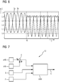
- FIG 6 an example of an arm current curve for a first arm current In and a second arm current Ip of one of the converter branches is shown.
- the diagram of the Figure 6 has a first axis I, on which the current intensity is plotted in any normalized units, and a second axis t, on which time is plotted in any units. Up to an excellent point in time t0, the diagram shows curves of the arm currents without a circulating current being generated. It can be seen that the curves of the arm currents each do not have a zero crossing.
- a circulating current is generated in the converter, which is a sinusoidal current (has a sinusoidal shape), namely with a frequency of 100 Hz Circulating current now has the recognizable effect that the arm currents Ip and In have zero crossings in their curves.
- FIG 7 is part of a control device 12 of the converter arrangement 1 of Figure 1 shown.
- a group balancing module GBM is provided.
- the group balancing module GBM On the input side of the group balancing module GBM, a difference between the switching module voltages or the energy storage voltages vVB of the full-bridge switching modules (or the average energy storage voltage of the full-bridge switching modules) and the switching module voltages or the energy storage voltages vHB of the half-bridge switching modules (or the average energy storage voltage of all the half-bridge switching modules) is supplied a differentiator D has been determined.
- the arm currents I of the converter arms are fed to the group balancing module GBM.
- the group balancing module GBM is provided with an information signal that contains information about a transient network state. Depending on the information available, the group balancing module GBM generates an instruction S for generating one or more superimposed converter circuit currents, which can be implemented by downstream parts of the control device 12.
Applications Claiming Priority (1)
| Application Number | Priority Date | Filing Date | Title |
|---|---|---|---|
| DE102019203407.1A DE102019203407A1 (de) | 2019-03-13 | 2019-03-13 | Stromrichteranordnung sowie Verfahren zu deren Betrieb |
Publications (3)
| Publication Number | Publication Date |
|---|---|
| EP3709498A2 true EP3709498A2 (fr) | 2020-09-16 |
| EP3709498A3 EP3709498A3 (fr) | 2020-09-23 |
| EP3709498B1 EP3709498B1 (fr) | 2024-05-01 |
Family
ID=69743087
Family Applications (1)
| Application Number | Title | Priority Date | Filing Date |
|---|---|---|---|
| EP20160322.2A Active EP3709498B1 (fr) | 2019-03-13 | 2020-03-02 | L'équilibrage des tensions sous-modules dans les bras d'un convertisseur modulaire à plusieurs niveaux fonctionnant à un indice de modulation élevé |
Country Status (2)
| Country | Link |
|---|---|
| EP (1) | EP3709498B1 (fr) |
| DE (1) | DE102019203407A1 (fr) |
-
2019
- 2019-03-13 DE DE102019203407.1A patent/DE102019203407A1/de not_active Withdrawn
-
2020
- 2020-03-02 EP EP20160322.2A patent/EP3709498B1/fr active Active
Also Published As
| Publication number | Publication date |
|---|---|
| DE102019203407A1 (de) | 2020-09-17 |
| EP3709498A3 (fr) | 2020-09-23 |
| EP3709498B1 (fr) | 2024-05-01 |
Similar Documents
| Publication | Publication Date | Title |
|---|---|---|
| EP2122817A1 (fr) | Asservissement d'une branche de module de phase d'un convertisseur à plusieurs niveaux | |
| EP3734818B1 (fr) | Procédé de traitement d'un défaut dans une conduite de tension continue ainsi que dispositif convertisseur de courant permettant la mise en oeuvre dudit procédé | |
| EP2845288B1 (fr) | Couplage ou découplage de puissance dans une dérivation à un noeud de un réseau dc par une source de tension connectée en série | |
| DE1438654A1 (de) | Elektrische Speisestromkreisanordnung | |
| EP2845303B1 (fr) | Convertisseur et procédés de conversion de tension | |
| WO2014206704A1 (fr) | Ensemble mutateur à mutateurs multi-étages câblés en parallèle et son procédé de commande | |
| EP0208088A1 (fr) | Dispositif pur l'obtention d'un système de tensions triphasées avec conducteur neutre chargeable | |
| EP0521901A1 (fr) | Dispositif d'alimentation ininterrompue en courant electrique. | |
| EP3622621B1 (fr) | Onduleur à plusieurs niveaux | |
| EP2966769B1 (fr) | Fonctionnement d'un convertisseur multi-étagé modulaire | |
| EP3709498B1 (fr) | L'équilibrage des tensions sous-modules dans les bras d'un convertisseur modulaire à plusieurs niveaux fonctionnant à un indice de modulation élevé | |
| EP3751718B1 (fr) | Procédé de traitement de défauts dans une ligne de tension continue ainsi que dispositif convertisseur de courant permettant la mise en oeuvre dudit procédé | |
| DE102019105196B4 (de) | Verfahren zur Strombegrenzung bei transienten Spannungsänderungen an einem Wechselstromausgang eines Multilevel-Wechselrichters und Multilevel-Wechselrichter | |
| WO2018113926A1 (fr) | Convertisseur | |
| EP3331118B1 (fr) | Installation de transfert d'énergie électrique | |
| DE102008036809A1 (de) | Redundanzsteuerverfahren eines mehrphasigen Stromrichters mit verteilten Energiespeichern | |
| EP3639352B1 (fr) | Ensemble convertisseur de puissance présentant une capacité de coupure d'un courant de fuite et procédé pour la coupure d'un courant de fuite pour ledit ensemble convertisseur de puissance | |
| EP3449554B1 (fr) | Onduleur et procédé pour générer un courant alternatif | |
| EP3994792A1 (fr) | Procédé de précharge de modules d'un convertisseur multiniveau modulaire | |
| WO2014127829A1 (fr) | Prélèvement en série avec unité de précharge | |
| DE3907940A1 (de) | Verfahren zur symmetrierung der spannungsaufteilung an stromrichtern mit mehrpunktschaltung | |
| EP0491690B1 (fr) | Procede de reglage par impulsion pour un onduleur a plusieurs etages | |
| EP4092895A1 (fr) | Procédé de fonctionnement d'un régulateur de courant continu destinés à l'alimentation d'un dispositif d'électrolyse en énergie électrique de fonctionnement | |
| WO2016050720A1 (fr) | Redresseur hybride à diodes m2c | |
| DE102021119899A1 (de) | Verfahren zum betrieb eines wechselrichters und wechselrichter |
Legal Events
| Date | Code | Title | Description |
|---|---|---|---|
| PUAI | Public reference made under article 153(3) epc to a published international application that has entered the european phase |
Free format text: ORIGINAL CODE: 0009012 |
|
| STAA | Information on the status of an ep patent application or granted ep patent |
Free format text: STATUS: THE APPLICATION HAS BEEN PUBLISHED |
|
| PUAL | Search report despatched |
Free format text: ORIGINAL CODE: 0009013 |
|
| AK | Designated contracting states |
Kind code of ref document: A2 Designated state(s): AL AT BE BG CH CY CZ DE DK EE ES FI FR GB GR HR HU IE IS IT LI LT LU LV MC MK MT NL NO PL PT RO RS SE SI SK SM TR |
|
| AX | Request for extension of the european patent |
Extension state: BA ME |
|
| AK | Designated contracting states |
Kind code of ref document: A3 Designated state(s): AL AT BE BG CH CY CZ DE DK EE ES FI FR GB GR HR HU IE IS IT LI LT LU LV MC MK MT NL NO PL PT RO RS SE SI SK SM TR |
|
| AX | Request for extension of the european patent |
Extension state: BA ME |
|
| RIC1 | Information provided on ipc code assigned before grant |
Ipc: H02M 7/483 20070101AFI20200820BHEP |
|
| RAP1 | Party data changed (applicant data changed or rights of an application transferred) |
Owner name: SIEMENS ENERGY GLOBAL GMBH & CO. KG |
|
| STAA | Information on the status of an ep patent application or granted ep patent |
Free format text: STATUS: REQUEST FOR EXAMINATION WAS MADE |
|
| 17P | Request for examination filed |
Effective date: 20210304 |
|
| RBV | Designated contracting states (corrected) |
Designated state(s): AL AT BE BG CH CY CZ DE DK EE ES FI FR GB GR HR HU IE IS IT LI LT LU LV MC MK MT NL NO PL PT RO RS SE SI SK SM TR |
|
| GRAP | Despatch of communication of intention to grant a patent |
Free format text: ORIGINAL CODE: EPIDOSNIGR1 |
|
| STAA | Information on the status of an ep patent application or granted ep patent |
Free format text: STATUS: GRANT OF PATENT IS INTENDED |
|
| INTG | Intention to grant announced |
Effective date: 20231127 |
|
| GRAS | Grant fee paid |
Free format text: ORIGINAL CODE: EPIDOSNIGR3 |
|
| GRAA | (expected) grant |
Free format text: ORIGINAL CODE: 0009210 |
|
| STAA | Information on the status of an ep patent application or granted ep patent |
Free format text: STATUS: THE PATENT HAS BEEN GRANTED |
|
| AK | Designated contracting states |
Kind code of ref document: B1 Designated state(s): AL AT BE BG CH CY CZ DE DK EE ES FI FR GB GR HR HU IE IS IT LI LT LU LV MC MK MT NL NO PL PT RO RS SE SI SK SM TR |
|
| REG | Reference to a national code |
Ref country code: GB Ref legal event code: FG4D Free format text: NOT ENGLISH |