EP3709493A1 - Test system and test method for power conversion device - Google Patents
Test system and test method for power conversion device Download PDFInfo
- Publication number
- EP3709493A1 EP3709493A1 EP18877150.5A EP18877150A EP3709493A1 EP 3709493 A1 EP3709493 A1 EP 3709493A1 EP 18877150 A EP18877150 A EP 18877150A EP 3709493 A1 EP3709493 A1 EP 3709493A1
- Authority
- EP
- European Patent Office
- Prior art keywords
- power conversion
- terminal
- conversion device
- power
- testing
- Prior art date
- Legal status (The legal status is an assumption and is not a legal conclusion. Google has not performed a legal analysis and makes no representation as to the accuracy of the status listed.)
- Granted
Links
Images






Classifications
-
- G—PHYSICS
- G01—MEASURING; TESTING
- G01R—MEASURING ELECTRIC VARIABLES; MEASURING MAGNETIC VARIABLES
- G01R31/00—Arrangements for testing electric properties; Arrangements for locating electric faults; Arrangements for electrical testing characterised by what is being tested not provided for elsewhere
- G01R31/40—Testing power supplies
-
- H—ELECTRICITY
- H02—GENERATION; CONVERSION OR DISTRIBUTION OF ELECTRIC POWER
- H02M—APPARATUS FOR CONVERSION BETWEEN AC AND AC, BETWEEN AC AND DC, OR BETWEEN DC AND DC, AND FOR USE WITH MAINS OR SIMILAR POWER SUPPLY SYSTEMS; CONVERSION OF DC OR AC INPUT POWER INTO SURGE OUTPUT POWER; CONTROL OR REGULATION THEREOF
- H02M3/00—Conversion of DC power input into DC power output
- H02M3/22—Conversion of DC power input into DC power output with intermediate conversion into AC
- H02M3/24—Conversion of DC power input into DC power output with intermediate conversion into AC by static converters
- H02M3/28—Conversion of DC power input into DC power output with intermediate conversion into AC by static converters using discharge tubes with control electrode or semiconductor devices with control electrode to produce the intermediate AC
- H02M3/325—Conversion of DC power input into DC power output with intermediate conversion into AC by static converters using discharge tubes with control electrode or semiconductor devices with control electrode to produce the intermediate AC using devices of a triode or a transistor type requiring continuous application of a control signal
- H02M3/335—Conversion of DC power input into DC power output with intermediate conversion into AC by static converters using discharge tubes with control electrode or semiconductor devices with control electrode to produce the intermediate AC using devices of a triode or a transistor type requiring continuous application of a control signal using semiconductor devices only
- H02M3/33569—Conversion of DC power input into DC power output with intermediate conversion into AC by static converters using discharge tubes with control electrode or semiconductor devices with control electrode to produce the intermediate AC using devices of a triode or a transistor type requiring continuous application of a control signal using semiconductor devices only having several active switching elements
- H02M3/33576—Conversion of DC power input into DC power output with intermediate conversion into AC by static converters using discharge tubes with control electrode or semiconductor devices with control electrode to produce the intermediate AC using devices of a triode or a transistor type requiring continuous application of a control signal using semiconductor devices only having several active switching elements having at least one active switching element at the secondary side of an isolation transformer
-
- H—ELECTRICITY
- H02—GENERATION; CONVERSION OR DISTRIBUTION OF ELECTRIC POWER
- H02M—APPARATUS FOR CONVERSION BETWEEN AC AND AC, BETWEEN AC AND DC, OR BETWEEN DC AND DC, AND FOR USE WITH MAINS OR SIMILAR POWER SUPPLY SYSTEMS; CONVERSION OF DC OR AC INPUT POWER INTO SURGE OUTPUT POWER; CONTROL OR REGULATION THEREOF
- H02M3/00—Conversion of DC power input into DC power output
- H02M3/22—Conversion of DC power input into DC power output with intermediate conversion into AC
- H02M3/24—Conversion of DC power input into DC power output with intermediate conversion into AC by static converters
- H02M3/28—Conversion of DC power input into DC power output with intermediate conversion into AC by static converters using discharge tubes with control electrode or semiconductor devices with control electrode to produce the intermediate AC
- H02M3/325—Conversion of DC power input into DC power output with intermediate conversion into AC by static converters using discharge tubes with control electrode or semiconductor devices with control electrode to produce the intermediate AC using devices of a triode or a transistor type requiring continuous application of a control signal
- H02M3/335—Conversion of DC power input into DC power output with intermediate conversion into AC by static converters using discharge tubes with control electrode or semiconductor devices with control electrode to produce the intermediate AC using devices of a triode or a transistor type requiring continuous application of a control signal using semiconductor devices only
- H02M3/337—Conversion of DC power input into DC power output with intermediate conversion into AC by static converters using discharge tubes with control electrode or semiconductor devices with control electrode to produce the intermediate AC using devices of a triode or a transistor type requiring continuous application of a control signal using semiconductor devices only in push-pull configuration
-
- H—ELECTRICITY
- H02—GENERATION; CONVERSION OR DISTRIBUTION OF ELECTRIC POWER
- H02M—APPARATUS FOR CONVERSION BETWEEN AC AND AC, BETWEEN AC AND DC, OR BETWEEN DC AND DC, AND FOR USE WITH MAINS OR SIMILAR POWER SUPPLY SYSTEMS; CONVERSION OF DC OR AC INPUT POWER INTO SURGE OUTPUT POWER; CONTROL OR REGULATION THEREOF
- H02M7/00—Conversion of AC power input into DC power output; Conversion of DC power input into AC power output
- H02M7/02—Conversion of AC power input into DC power output without possibility of reversal
- H02M7/04—Conversion of AC power input into DC power output without possibility of reversal by static converters
- H02M7/12—Conversion of AC power input into DC power output without possibility of reversal by static converters using discharge tubes with control electrode or semiconductor devices with control electrode
- H02M7/21—Conversion of AC power input into DC power output without possibility of reversal by static converters using discharge tubes with control electrode or semiconductor devices with control electrode using devices of a triode or transistor type requiring continuous application of a control signal
- H02M7/217—Conversion of AC power input into DC power output without possibility of reversal by static converters using discharge tubes with control electrode or semiconductor devices with control electrode using devices of a triode or transistor type requiring continuous application of a control signal using semiconductor devices only
- H02M7/219—Conversion of AC power input into DC power output without possibility of reversal by static converters using discharge tubes with control electrode or semiconductor devices with control electrode using devices of a triode or transistor type requiring continuous application of a control signal using semiconductor devices only in a bridge configuration
-
- H—ELECTRICITY
- H02—GENERATION; CONVERSION OR DISTRIBUTION OF ELECTRIC POWER
- H02M—APPARATUS FOR CONVERSION BETWEEN AC AND AC, BETWEEN AC AND DC, OR BETWEEN DC AND DC, AND FOR USE WITH MAINS OR SIMILAR POWER SUPPLY SYSTEMS; CONVERSION OF DC OR AC INPUT POWER INTO SURGE OUTPUT POWER; CONTROL OR REGULATION THEREOF
- H02M7/00—Conversion of AC power input into DC power output; Conversion of DC power input into AC power output
- H02M7/42—Conversion of DC power input into AC power output without possibility of reversal
- H02M7/44—Conversion of DC power input into AC power output without possibility of reversal by static converters
- H02M7/48—Conversion of DC power input into AC power output without possibility of reversal by static converters using discharge tubes with control electrode or semiconductor devices with control electrode
- H02M7/483—Converters with outputs that each can have more than two voltages levels
- H02M7/4835—Converters with outputs that each can have more than two voltages levels comprising two or more cells, each including a switchable capacitor, the capacitors having a nominal charge voltage which corresponds to a given fraction of the input voltage, and the capacitors being selectively connected in series to determine the instantaneous output voltage
-
- H—ELECTRICITY
- H02—GENERATION; CONVERSION OR DISTRIBUTION OF ELECTRIC POWER
- H02M—APPARATUS FOR CONVERSION BETWEEN AC AND AC, BETWEEN AC AND DC, OR BETWEEN DC AND DC, AND FOR USE WITH MAINS OR SIMILAR POWER SUPPLY SYSTEMS; CONVERSION OF DC OR AC INPUT POWER INTO SURGE OUTPUT POWER; CONTROL OR REGULATION THEREOF
- H02M1/00—Details of apparatus for conversion
- H02M1/0067—Converter structures employing plural converter units, other than for parallel operation of the units on a single load
- H02M1/0077—Plural converter units whose outputs are connected in series
Definitions
- the present invention relates to a system and method for testing a power conversion device, and more particularly to testing a power conversion device which performs direct current (DC) voltage conversion with an input and an output both being DC voltage.
- DC direct current
- Patent Literature 1 US Patent US 5 027 264 A discloses that a configuration including two single- or three-phase full bridge circuits and a transformer is suitable for high power applications. Specifically, for the two full-bridge circuits, a DC terminal is connected to an input terminal or an output terminal of DC voltage, and an alternate current (AC) terminal is connected to a primary side winding or a secondary side winding of the transformer. This implements a power conversion device capable of DC/DC conversion with the primary side and the secondary side electrically insulated. Further, PTL 1 describes suppressing power loss by applying soft switching to semiconductor switching elements constituting each full bridge circuit.
- NPL 1 Rik W.A.A. De Doncker et. al., "A Three-Phase Soft-Switched High-Power-Density dc/dc Converter for High-Power Applications," IEEE TRANSACTIONS ON INDUSTRY APPLICATIONS, VOL. 27, NO. 1, JANUARY/FEBRUARY 1991 .
- Testing a power conversion device such as described in PTL 1, requires a testing power supply and peripheral devices such as a protective circuit breaker and a measuring instrument.
- testing a power conversion device for high power applications entails a testing power supply and peripheral devices having increased rated capacities, and a test system increased in size and cost is a matter of concern.
- the present invention has been made to solve such a problem, and an object of the present invention is to provide a system and method for efficiently testing a power conversion device which performs DC/DC conversion.
- a power conversion device test system includes at least one power conversion device which is a test target, a testing power supply for testing the test target, and first and second connection members.
- Each power conversion device performs DC voltage conversion between a primary side DC terminal and a secondary side DC terminal for inputting and outputting DC voltage.
- the first connection member connects the testing power supply and an input side of the test target.
- the second connection member electrically connects an output side of the test target and the testing power supply. Active power output from the output side of the test target is transmitted to the input side of the test target by the second connection member.
- a method for testing a power conversion device is a method in which at least one power conversion device is a test target, each power conversion device performing DC voltage conversion between a primary side DC terminal and a secondary side DC terminal for inputting and outputting DC voltage.
- the test target from the testing power supply electrically connected to the input side of the test target by the first connection member, the test target, with its input and output sides electrically connected via the second connection member, is supplied via the first connection member with active power smaller than active power which passes through the test target.
- the power conversion device by supplying from a testing power supply active power smaller than active power passing through a power conversion device, which is a test target, the power conversion device can be efficiently tested.
- FIG. 1 is a block diagram for illustrating a first example of a power conversion device which is a test target.
- a power conversion device 100a according to the first example includes primary side DC terminals 1a and 1b, secondary side DC terminals 2a and 2b, and a plurality of converter cells 10.
- Converter cells 10 each perform DC/DC conversion.
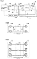
- FIG. 2 is a circuit diagram for illustrating a first example configuration of converter cell 10 shown in FIG. 1 .
- converter cell 10 according to the first example configuration includes capacitors 6 and 7, a single-phase transformer 8, a first switching circuit 41, a second switching circuit 42, and a control circuit 45.
- Control circuit 45 can be composed of dedicated hardware such as an analog circuit or an ASIC (Application Specific Integrated Circuit). Alternatively, control circuit 45 may have its functions partially or entirely implemented by software processing by a processor (not shown) executing a program installed in a memory (not shown).
- Transformer 8 includes a single-phase primary side winding 8x connected to primary side AC nodes 81a and 81b, and a single-phase secondary side winding 8y connected to secondary side AC nodes 82a and 82b.
- Capacitor 6 is connected between primary side DC nodes 11a and 11b.
- Capacitor 7 is connected between secondary side DC nodes 12a and 12b.
- First switching circuit 41 is connected between primary side DC nodes 11a and 11b and primary side AC nodes 81a and 81b.
- First switching circuit 41 includes semiconductor switching elements Q11 to Q14 connected in a single-phase full bridge, and freewheeling diodes D11 to D14 connected to semiconductor switching elements Q11 to Q14 in antiparallel.
- second switching circuit 42 is connected between secondary side DC nodes 12a and 12b and secondary side AC nodes 82a and 82b.
- Second switching circuit 42 includes semiconductor switching elements Q21 to Q24 connected in a single-phase full bridge, and freewheeling diodes D21 to D24 connected to semiconductor switching elements Q21 to Q24 in antiparallel.
- Semiconductor switching elements Q11 to Q14 and Q21 to Q24 can each be composed of a self arc-extinguishing switching element such as an IGBT (Insulated Gate Bipolar Transistor). Turning on/off semiconductor switching elements Q11 to Q14 and Q21 to Q24 can be controlled by control signals S11 to S14 and S21 to S24, respectively, issued from control circuit 45.
- IGBT Insulated Gate Bipolar Transistor
- Turning on/off semiconductor switching elements Q11 to Q14 is controlled so as to perform power conversion (DC/AC conversion) between DC voltage Vc1 of primary side DC nodes 11a and 11b and AC voltage (single phase) V41 of primary side AC nodes 81a and 81b.
- turning on/off semiconductor switching elements Q21 to Q24 is controlled so as to perform power conversion (AC/DC conversion) between AC voltage (single phase) V42 of secondary side AC nodes 82a and 82b and DC voltage Vc2 of secondary side DC nodes 12a and 12b.
- converter cell 10 is configured as a so-called single-phase DAB (Dual-Active Bridge) that converts DC voltage to DC voltage via single-phase AC voltage transmitted via insulation by transformer 8.
- First switching circuit 41 corresponds to an embodiment of a "first power conversion unit” and second switching circuit 42 corresponds to an embodiment of a "second power conversion unit.”
- turning on/off semiconductor switching elements Q11 to Q14 and Q21 to Q24 can be controlled to control AC voltages V41 and V42 in amplitude and phase to control power transmission between the primary side and the secondary side in amount and direction, as desired. This is done in a known method, which is described for example in NPL 1.
- control circuit 45 can detect temperatures TQ11 to TQ14 and TQ21 to TQ24 of semiconductor switching elements Q11 to Q14 and Q21 to Q24 and temperatures TD11 to TD14 and TD21 to TD24 of freewheeling diodes D11 to D14 and D21 to D24. Furthermore, disposing a voltage sensor (not shown) for capacitors 6 and 7 enables control circuit 45 to detect DC voltages Vc1 and Vc2. Similarly, disposing a current sensor (not shown) for transformer 3 enables control circuit 45 to also detect an AC current (single phase) passing through transformer 3.
- FIG. 3 shows a second example configuration of converter cell 10 shown in FIG. 1 .
- converter cell 10 according to the second example configuration includes a three-phase transformer 3, capacitors 6 and 7, a first switching circuit 51, a second switching circuit 52, and a control circuit 55.
- control circuit 55 can also have its functions implemented by dedicated hardware and/or software processing by executing a program.
- Transformer 3 includes a three-phase primary side winding (not shown) connected to primary side AC nodes 31a, 31b, 31c and a three-phase secondary side winding (not shown) connected to secondary side AC nodes 32a, 32b, 32c.
- Capacitor 6 is connected between primary side DC nodes 11a and 11b and capacitor 7 is connected between secondary side DC nodes 12a and 12b, similarly as shown in FIG. 2 .
- First switching circuit 51 is connected between primary side DC nodes 11a, 11b and secondary side AC nodes 32a, 32b, 32c.
- First switching circuit 51 includes semiconductor switching elements Q61 to Q66 connected in a three-phase full bridge, and freewheeling diodes D61 to D66 connected to semiconductor switching elements Q61 to Q66 in antiparallel.
- second switching circuit 52 is connected between secondary side DC nodes 12a, 12b and secondary side AC nodes 32a, 32b, 32c.
- Second switching circuit 52 includes semiconductor switching elements Q71 to Q76 connected in a three-phase full bridge, and freewheeling diodes D71 to D76 connected to semiconductor switching elements Q71 to Q76 in antiparallel.
- Semiconductor switching elements Q61 to Q66 and Q71 to Q76 can each also be composed of a self arc-extinguishing switching element such as an IGBT (Insulated Gate Bipolar Transistor). Turning on/off semiconductor switching elements Q61 to Q66 and Q71 to Q76 can be controlled by control signals S61 to S66 and S71 to S76, respectively, issued from control circuit 55.
- IGBT Insulated Gate Bipolar Transistor
- Turning on/off semiconductor switching elements Q61 to Q66 is controlled so as to perform power conversion (DC/AC conversion) between DC voltage Vc1 of primary side DC nodes 11a and 11b and AC voltage (three phases) of primary side AC nodes 31a, 31b, 31c.
- turning on/off semiconductor switching elements Q71 to Q76 is controlled so as to perform power conversion (AC/DC conversion) between AC voltage (three phases) of secondary side AC nodes 32a, 32b, 32c and DC voltage Vc2 of secondary side DC nodes 12a and 12b.
- converter cell 10 is configured as a so-called 3-phase DAB (Dual-Active Bridge) that converts DC voltage to DC voltage via 3-phase AC voltage transmitted via insulation by transformer 3.
- First switching circuit 51 corresponds to an embodiment of the "first power conversion unit”
- second switching circuit 52 corresponds to an embodiment of the "second power conversion unit.”
- turning on/off semiconductor switching elements Q61 to Q66 and Q71 to Q76 can be controlled to control 3-phase AC voltage in amplitude and phase to control power transmission between the primary side and the secondary side in amount and direction, as desired. This is done in a known method, which is described for example in NPL 1.
- control circuit 55 can detect temperatures TQ61 to TQ66 and TQ71 to TQ76 of semiconductor switching elements Q61 to Q66 and Q71 to Q76 and temperatures TD61 to TD66 and TD71 to TD76 of freewheeling diodes D61 to D66 and D71 to D76. It is also possible to dispose a voltage sensor (not shown) for capacitors 6 and 7 and dispose a current sensor (not shown) for transformer 8. Thereby, control circuit 45 can further detect DC voltages Vc1 and Vc2 and an AC current (three phases) passing through transformer 8.
- a plurality of converter cells 10 each have primary side DC nodes 11a and 11b connected to primary side DC terminals 1a and 1b in parallel.
- the plurality of converter cells 10 On the secondary side of power conversion device 100a, the plurality of converter cells 10 have secondary side DC nodes 12a and 12b connected in series between secondary side DC terminals 2a and 2b.
- power conversion device 100a while power of a large current can be handled on the primary side, power of high voltage can be handled on the secondary side. Furthermore, DC power of low voltage can be converted to DC power of high voltage.
- FIG. 4 is a block diagram for illustrating a second example of a power conversion device which is a test target.
- a power conversion device 100b according to the second example is similar to power conversion device 100a, that is, it includes primary side DC terminals 1a and 1b, secondary side DC terminals 2a and 2b, and a plurality of converter cells 10.
- the plurality of converter cells 10 are connected in series on both the primary side and the secondary side.
- the plurality of converter cells 10 each have primary side DC nodes 11a and 1 1b connected in series between primary side DC terminals 1a and 1b.
- the plurality of converter cells 10 On the secondary side of power conversion device 100b as well, the plurality of converter cells 10 have secondary side DC nodes 12a and 12b connected in series between secondary side DC terminals 2a and 2b.
- DC voltage of high voltage can be handled on both the primary side and the secondary side.
- DC voltage between primary side DC terminals 1a and 1 and DC voltage between secondary side DC terminals 2a and 2b will be equivalent.
- FIG. 5 is a block diagram for illustrating a third example of a power conversion device which is a test target.
- a power conversion device 100c according to the third example is similar to power conversion devices 100a and 100b, that is, it includes primary side DC terminals 1a and 1b, secondary side DC terminals 2a and 2b, and a plurality of converter cells 10.
- the plurality of converter cells 10 are connected in parallel on both the primary side and the secondary side.
- the plurality of converter cells 10 each have primary side DC nodes 11a and 11b connected to primary side DC terminals 1a and 1b in parallel.
- the plurality of converter cells 10 On the secondary side of power conversion device 100c as well, the plurality of converter cells 10 have secondary side DC nodes 12a and 12b connected to secondary side DC terminals 2a and 2b in parallel.
- DC voltage of a large current can be handled on both the primary side and the secondary side.
- DC voltage between primary side DC terminals 1a and 1b and DC voltage between secondary side DC terminals 2a and 2b will be equivalent.
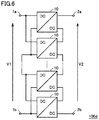
- FIG. 6 is a block diagram for illustrating a fourth example of a power conversion device which is a test target.
- a power conversion device 100d according to the third example is similar to power conversion devices 100a to 100c, that is, it includes primary side DC terminals 1a and 1b, secondary side DC terminals 2a and 2b, and a plurality of converter cells 10.
- the plurality of converter cells 10 On the secondary side of power conversion device 100d, as well as power conversion device 100b (see FIG. 4 ), the plurality of converter cells 10 have secondary side DC nodes 12a and 12b connected in series between secondary side DC terminals 2a and 2b.
- every two converter cells 10 On the primary side of power conversion device 100d, every two converter cells 10 have primary side DC nodes 11a and 11b connected in parallel, and furthermore, primary side DC nodes 11a and 11b of every two converter cells 10 that are connected in parallel are connected in series between primary side DC terminals 1a and 1b. That is, on the primary side, the plurality of converter cells 10 are connected in series-parallel.
- intermediate DC voltage higher than the primary side of power converter (see FIG. 5 ) 100c and lower than power conversion device 100b (see FIG. 4 ) can be handled by using the same number of converter cells 10.
- the intermediate DC voltage on the primary side can be converted on the secondary side to high voltage equivalent to that of power conversion device 100b.
- power conversion device 100 having a plurality of converter cells 10, including power conversion devices 100a to 100d described with reference to in FIGS. 1 and 4 to 6 are test targets. That is, power conversion device 100 includes power conversion devices 100a to 100d described above, and includes a plurality of converter cells 10 arranged in any number in any connection manner (series, parallel, or series-parallel).
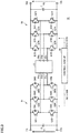
- FIG. 7 is a block diagram for illustrating an example configuration of a test system 5a to test a power conversion device according to the first embodiment.
- power conversion device 100 shown in FIG. 7 is an embodiment of a "first power conversion device.”
- Test system 5a includes a DC power supply 201 which is an example of the "testing power supply,” a testing circuit breaker 205, measuring instruments 206 to 209, power cables PL1 and PL2, and a control device 250.
- DC power supply 201 which is an example of the "testing power supply”
- testing circuit breaker 205 measuring instruments 206 to 209
- power cables PL1 and PL2 power cables PL1 and PL2, and a control device 250.
- primary side DC terminals 1a and 1b correspond to an "input side”
- secondary side DC terminals 2a and 2b correspond to an "output side.”
- Power cable PL1 electrically connects DC power supply 201 and primary side DC terminals 1a and 1b of power conversion device 100.
- Power cable PL2 has one end connected to secondary side DC terminals 2a and 2b of power conversion device 100 and the other end electrically connected to power cable PL1.
- power cable PL2 electrically connects secondary side DC terminals 2a and 2b of power conversion device 100 and DC power supply 201. That is, power cable PL1 corresponds to an embodiment of a "first connection member" and power cable PL2 corresponds to an embodiment of a "second connection member.”
- Circuit breaker 205 is connected in series with power cable PL1. Circuit breaker 205 has a protective function to interrupt or form a current path in response to an open/close command received from control device 250 and automatically interrupt the current path when a value of a current exceeds a predetermined reference value.
- Measuring instrument 206 detects output voltage (power supply voltage) of DC power supply 201.
- Measuring instrument 207 measures an output current (a power supply current) of DC power supply 201.
- Measuring instrument 208 is connected to power cable PL1 and measures a current passing through primary side DC terminals 1a and 1b.
- Measuring instrument 209 is connected to power cable PL2 and measures a current passing through secondary side DC terminals 2a and 2b. Measurement values obtained by measuring instruments 206 to 209 are input to control device 250.
- Control circuit 250 can also have its functions configured by dedicated hardware such as an analog circuit, an ASIC or the like. Alternatively, control circuit 250 may be composed of a microcomputer or the like having a computing function and have its functions partially or entirely implemented by software processing by a processor (not shown) executing a program installed in a memory (not shown).
- control device 250 can generate a command value for DC power supply 201, a command to open/close circuit breaker 205, and a command value for power conversion device 100. Thereby, in testing power conversion device 100, an output of DC power supply 201, opening/closing circuit breaker 205, and an operation in power conversion device 100 (for example, turning on/off the semiconductor switching elements constituting converter cell 10) can be controlled. Further, a value detected in power conversion device 100, e.g., a value in temperature detected in testing the semiconductor switching elements and the freewheeling diodes, as has been described with reference to FIGS. 3 and 4 , can also be input to control device 250.
- a value detected in power conversion device 100 e.g., a value in temperature detected in testing the semiconductor switching elements and the freewheeling diodes, as has been described with reference to FIGS. 3 and 4 , can also be input to control device 250.
- Pi - Po corresponds to power loss in power conversion device 100, and it is understood that this power loss is equivalent to active power Ps supplied from DC power supply 201.
- Active power Ps can be measured using measuring instruments 206 and 207.
- active power Pi can be measured using measuring instruments 206 and 208, and active power Po can be measured using measuring instruments 206 and 209.
- test system 5a can test power conversion device 100 by supplying active power Ps smaller than active power Po passing through power conversion device 100.
- This allows a testing power supply (DC power supply 201), circuit breaker 205, and measuring instrument 207 to have reduced rated capacities.
- test system 5a can be reduced in size and cost, and power conversion device 100 can be efficiently tested.
- FIG. 8 is a conceptual diagram for illustrating an operation of converter cell 10 shown in FIG. 2 when a test is conducted.
- FIG. 8 shows an AC equivalent circuit of a single-phase DAB.
- an equivalent voltage source 410 is configured by turning on/off semiconductor switching elements Q11 to Q14 in first switching circuit 41.
- Equivalent voltage source 410 outputs AC voltage (line voltage) V41 to primary side AC nodes 81a and 81b of transformer 8, as has been shown in FIG. 2 .
- an equivalent voltage source 420 is configured by turning on/off semiconductor switching elements Q21 to Q24 in second switching circuit 42.
- Equivalent voltage source 420 outputs AC voltage (line voltage) V42 to secondary side AC nodes 82a and 82b of transformer 8, as has been shown in FIG. 2 .
- Equivalent voltage sources 410 and 420 are equivalently connected via an equivalent inductance 80.
- Equivalent inductance 80 corresponds to leakage inductance of transformer 8.
- the inductance of the inductor is also included in equivalent inductance 80.
- line voltages V41 and 42 can be controlled in phase and amplitude, as desired, by controlling turning on/off semiconductor switching elements Q11 to Q14 in first switching circuit 41 and semiconductor switching elements Q21 to Q24 in second switching circuit 42.
- control circuit 45 By controlling a phase difference between line voltage V41 and line voltage V42, active power Pc passing through converter cell 10 can be controlled. Accordingly, by control circuit 45, control signals S11 to S14 and S21 to S24 can be generated to implement a switching pattern for semiconductor switching elements Q11 to Q14 and Q21 to Q24 for causing a phase difference following a command value for active power Pc.
- reactive power Qc generated in converter cell 10 can be controlled by controlling an amplitude difference between line voltage V41 and line voltage V42. Accordingly, by control circuit 45, control signals S11 to S14 and S21 to S24 can be generated to implement a switching pattern for semiconductor switching elements Q11 to Q14 and Q21 to Q24 for causing an amplitude difference following a command value for reactive power Qc.
- control signals S11 to S14 and S21 to S24 can be generated to control a switching pattern for semiconductor switching elements Q11 to Q14 and Q21 to Q24 in accordance with a combination of the command value for active power Pc and the command value for reactive power Qc.
- capacitors 6 and 7 are connected in parallel by power cables PL1 and PL2 and thus equal in voltage.
- one of first switching circuit 41 and second switching circuit 42 performs a zero voltage output operation. Specifically, in the zero voltage output operation, in first switching circuit 41, while semiconductor switching elements Q11, Q13 (or Q12, Q14) are turned on, semiconductor switching elements Q12, Q14 (or Q11, Q13) are turned off to zero a voltage difference between AC nodes 81a and 81b.
- second switching circuit 42 in the zero voltage output operation, while semiconductor switching elements Q21 and Q23 (or Q22 and Q24) are turned on, semiconductor switching elements Q22 and Q24 (or Q21 and Q23) are turned off to zero a voltage difference between secondary side AC nodes 82a and 82b.
- first switching circuit 41 and second switching circuit 42 a normal operation for outputting AC voltage (single phase) controlled in phase and amplitude can be performed to cause an amplitude difference between line voltage V41 and line voltage V42.
- reactive power Qc can also be generated in each converter cell 10 when a test is conducted in test system 5a of FIG. 7 .
- FIG. 9 is a conceptual diagram for illustrating an operation of converter cell 10 shown in FIG. 3 when a test is conducted.
- FIG. 9 shows an AC-side equivalent circuit of a three-phase DAB.
- an equivalent voltage source 510 is configured by turning on and off semiconductor switching elements Q61 to Q66 in first switching circuit 51.
- Equivalent voltage source 510 outputs AC voltages (line voltages) V51a to V51c to primary side AC nodes 31a, 31b, 31c of transformer 3, as has been shown in FIG. 2 .
- AC voltages (line voltages) V51a to V51c have a phase difference by 120 degrees.
- an equivalent voltage source 520 is configured by turning on and off semiconductor switching elements Q71 to Q76 in second switching circuit 52.
- Equivalent voltage source 520 outputs AC voltages (phase voltages) V52a to V52c to secondary side AC nodes 32a, 32b, 32c of transformer 3, as shown in FIG. 2 .
- AC voltages (phase voltages) V52a to V52c have a phase difference by 120 degrees.
- Equivalent voltage sources 510 and 520 are equivalently connected via an equivalent inductance 30.
- Equivalent inductance 30 corresponds to leakage inductance of transformer 3.
- the inductance of the inductor is also included in equivalent inductance 30.
- phase voltages V51a to V51c can be controlled in phase and amplitude, as desired, by controlling turning on/off semiconductor switching elements Q61 to Q66 in first switching circuit 51.
- phase voltages V52a to V52c can be controlled in phase and amplitude, as desired, by controlling turning on/off semiconductor switching elements Q71 to Q76 in second switching circuit 52.
- control signals S61 to S66 and S71 to S76 can be generated to implement a switching pattern for semiconductor switching elements Q61 to Q66 and Q71 to Q76 for causing a phase difference and/or an amplitude difference following a command value for at least one of active power Pc and reactive power Qc.
- converter cell 10 of FIG. 3 when first switching circuit 51 performs a zero voltage operation, while semiconductor switching elements Q61, Q63, Q65 (or Q62, Q64, Q66) are turned on, semiconductor switching elements Q62 Q64, Q66 (or Q61, Q63, Q65) are turned off to zero a voltage difference among primary side AC nodes 31a to 31c.
- second switching circuit 52 performs a zero voltage output operation, while semiconductor switching elements Q71, Q73, Q75 (or Q72, Q74, Q76) are turned on, semiconductor switching elements Q72, Q74, Q76 (or Q71, Q73, Q75) are turned off to zero a voltage difference among secondary side AC nodes 32a to 32c.
- reactive power Qc can be generated in each converter cell 10 by performing a zero voltage output operation in one of first switching circuit 51 and second switching circuit 52 and performing a normal operation in the other of first switching circuit 51 and second switching circuit 52 for outputting AC voltage (three phases) controlled in phase and amplitude.
- controllability of active power of power conversion device 100 and power loss of power conversion device 100 can be measured by measuring active power Pi input to primary side DC terminals 1a and 1b, active power Po output from secondary side DC terminals 2a and 2b, and active power Ps supplied from testing DC power supply 201 as shown in FIG. 7 in a state in which active power Pc of each converter cell 10 is controlled in response to a command value issued from control device 250, as has been described with reference to FIGS. 8 and 9 .
- test system 5a controllability of power conversion device 100 and whether an overcurrent is generated can be confirmed by measuring an AC current sensed by a current sensor disposed at transformer 3 (see FIG. 2 ) or transformer 8 (see FIG. 3 ).
- test system 5a whether a balance of currents of converter cells 10 can also be confirmed by measuring currents of primary side DC nodes 11a and 1 1b and secondary side DC nodes 12a and 12b of the plurality of converter cells 10. Further, whether a balance of voltages of converter cells 10 can also be confirmed by measuring the voltages of capacitors 6, 7 of the plurality of converter cells 10 (i.e., DC voltages Vc1, Vc2).
- test system 5a by conducting a heat run test by measuring the temperature of the semiconductor switching elements and freewheeling diodes constituting each converter cell 10, it can be confirmed whether the temperature falls within a range lower than a tolerable value.
- the tolerable value in the heat run test can be set to about 125 to 150°C.
- Reactive power is power which is generated inside power conversion device 100 and does not flow out of power conversion device 100.
- testing DC power supply 201 by generating reactive power, active power that testing DC power supply 201 supplies can be reduced, so that the rated capacities of the testing power supply (DC power supply 201), circuit breaker 205, and measuring instruments 207 to 209 can further be reduced, and the rated capacities of power cables PL1 and PL2 for connection for testing can also be reduced.
- reactive power can be easily generated by controlling turning on/off the semiconductor switching elements in each converter cell 10. As the reactive power is increased, the above effect is extended. For example, the reactive power in a test target or power conversion device 100 can be made larger than the active power passing through power conversion device 100.
- FIG. 10 is a block diagram for illustrating an example configuration of a test system 5b to test a power conversion device according to a modification of the first embodiment.
- power conversion device 100 shown in FIG. 10 is an embodiment of a "second power conversion device.”
- V1 V2 ⁇ V2.
- the two power conversion devices 100 one located on the left side in FIG. 10 will also be referred to as a preceding stage's power conversion device 100, and the other one located on the right side in FIG. 10 will also be referred to as a following stage's power conversion device 100.
- Power cable PL1 electrically connects DC power supply 201 and primary side DC terminals 1a and 1b of the preceding stage's power conversion device 100.
- Power cable PL2 has one end connected to secondary side DC terminals 2a and 2b of the following stage's power conversion device 100 and the other end electrically connected to power cable PL1.
- Power cable PL3 connects secondary side DC terminals 2a and 2b of the two power conversion devices 100 that input and output DC voltage V2.
- test system 5b of FIG. 10 primary side DC terminals 1a and 1b of the preceding stage's power conversion device 100 correspond to an input side of a test target, and primary side DC terminals 1a and 1b of the following stage's power conversion device 100 correspond to an output side of the test target. Therefore, in test system 5b as well, power cable PL1 corresponds to an embodiment of the "first connection member,” and power cable PL2 corresponds to an embodiment of the "second connection member.”
- Circuit breaker 205 and measuring instruments 206 and 207 are connected to power cable PL1 similarly as done in test system 5a.
- a measuring instrument 208 is further provided for measuring a current of primary side DC terminals 1a and 1b of the preceding stage's power conversion device 100.
- measuring instruments 210 and 211 are provided for measuring a DC current and a DC voltage (V2)
- measuring instruments 209 and 212 are provided for measuring a DC current and a DC voltage (VI).
- Measurement values obtained by measuring instruments 206 to 212 are input to control device 250.
- Active power Ps can be measured by measuring instruments 206 and 207
- active power Pi can be measured by measuring instruments 206 and 208
- active power Pm can be measured by measuring instruments 210 and 211
- active power Po can be measured by measuring instruments 209 and 212.
- control device 250 can generate a command value for each of the preceding and following stages' power conversion devices 100 for controlling an operation (i.e., power conversion).
- the command value includes the command values for active power Pc and reactive power Qc described in the first embodiment.
- the values of temperature, voltage, and a current sensed, as have been described in the first embodiment can be obtained from control circuits 45 and 55 for each power conversion device 100.
- the preceding stage's power conversion device 100 operates, as controlled, to increase DC voltage V1 input to primary side DC terminals 1a and 1b and output DC voltage V2 from secondary side DC terminals 2a and 2b.
- the following stage's power conversion device 100 operates, as controlled, to decrease DC voltage V2 input to secondary side DC terminals 2a and 2b and output DC voltage V1 from primary side DC terminals 1a and 1b.
- at least one of active power Pc and reactive power Qc is controlled in each of the preceding and following stages' power conversion devices 100.
- active power Pm is output from secondary side DC terminals 2a and 2b of the preceding stage's power conversion device 100 and input to secondary side DC terminals 2a and 2b of the following stage's power conversion device 100.
- Active power Po output from primary side DC terminals 1a and 1b of the following stage's power conversion device 100 is transmitted by power cable PL2 and will be a part of power input to the preceding stage's power conversion device 100.
- Pi - Pm corresponds to power lost in the preceding stage's power conversion device 100
- test system 5b can test a power conversion device by supplying active power Ps smaller than active power Po passing through a test target which is power conversion device 100 having different input and output voltages.
- This allows a testing power supply (DC power supply 201), circuit breaker 205, and measuring instrument 207 to have reduced rated capacities.
- test system 5b can be reduced in size and cost, and power conversion device 100 having different input and output voltages can be efficiently tested.
- the preceding stage's power conversion device 100 in a configuration in which primary side DC terminals 1a and 1b on the lower-voltage side (VI ⁇ V2) are connected to the testing power supply (DC power supply 201) allows a power supply having a low rated voltage to be used as the testing power supply (DC power supply 201). Furthermore, withstand voltage required for the testing power supply and power cables PL1 and PL2 is reduced, and test system 5b can further be reduced in size and cost by reducing an insulating member in size.
- each power conversion device 100 has specific contents which are similar to those in the first embodiment, including a heat run test and generation of reactive power, and accordingly, will not be described repeatedly in detail.
- test system 5b a power conversion operation in the preceding stage's power conversion device 100 in a direction in which primary side DC terminals 1a and 1b are an input and secondary side DC terminals 2a and 2b are an output, and a power conversion operation in the following stage's power conversion device 100 in a direction in which secondary side DC terminals 2a and 2b are an input and primary side DC terminals 1a and 1b are an output, can both be tested simultaneously. This allows the test to be conducted in a reduced period of time.
- the preceding stage's power conversion device 100 can control DC voltage V2 of secondary side DC terminals 2a and 2b and the following stage's power conversion device 100 can control active power Po.
- the following stage's power conversion device 100 can control DC voltage V2 of secondary side DC terminals 2a and 2b
- the preceding stage's power conversion device 100 can control active power Pm.
- FIG. 11 is a block diagram for illustrating an example configuration of a test system 5c to test a power conversion device according to the second embodiment.
- test system 5c includes AC power supply 301, testing circuit breaker 305, measuring instruments 206, 208, 209, 212, 306 to 308, testing converters 400a and 400b, cables PL1, PL2, PL10, PL11, and a control device 350.
- Control circuit 350 can also have its functions configured by dedicated hardware such as an analog circuit, an ASIC or the like.
- control circuit 350 may be composed of a microcomputer or the like having a computing function and have its functions partially or entirely implemented by software processing by a processor (not shown) executing a program installed in a memory (not shown).
- AC power supply 301 can be configured by a power supply device having a controllable output or an AC power system (for example, 6.6 kV).
- Testing converter 400a performs AC/DC conversion between AC voltage of AC power supply 301 and DC voltage V1 of primary side DC terminals 1a and 1b of power conversion device 100.
- Testing converter 400b performs DC/AC conversion between DC voltage V2 of secondary side DC terminals 2a and 2b of power conversion device 100 and AC voltage of AC power supply 301.
- FIG. 12 shows an example configuration of testing converters 400a and 400b shown in FIG. 11 .
- Testing converters 400a and 400b have the same configuration, and accordingly, hereinafter they will collectively, simply be referred to as a testing converter 400.
- testing converter 400 can be constituted by a modular multilevel converter which performs AC/DC power conversion or DC/AC power conversion bidirectionally between AC nodes 406u, 406v, 406v and DC nodes 407x, 407y.
- an arm circuit 430 in which a plurality of submodules 50 and a reactor are connected in series is arranged on each of a positive side and a negative side.
- three arm circuits 430 for U, V, and W phases (for the positive side) are connected between AC nodes 406u, 406v, and 406v, respectively, and DC node 407x.
- three arm circuits 430 for U, V, and W phases (for the negative side) are connected between AC nodes 406u, 406v, and 406v, respectively, and DC node 407y.
- a plurality of submodules 50 have output terminals 408x and 408y connected in series.
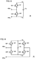
- FIG. 13 shows a first example configuration of submodule 50 shown in FIG. 12 .
- submodule 50 according to the first example configuration has a so-called half-bridge configuration.
- submodule 50 includes a pair of output terminals 408x and 408y, a capacitor Ca, semiconductor switching elements Q91 and Q92, and freewheeling diodes D91 and D92.
- Output terminal 408x, 408y is electrically connected to output terminal 408x, 408y of another submodule 50, AC node 406u, 406v, 406w, or DC node 407x, 407y for the series connection shown in FIG. 12 .
- Capacitor Ca is connected between node Nx and node Ny, semiconductor switching element Q91 is electrically connected between output terminal 408x and node Nx, and semiconductor switching element Q92 is electrically connected between output terminals 408x and 408y. Freewheeling diodes D91 and D92 are connected to semiconductor switching elements Q91 and Q92 in antiparallel.
- capacitor Ca is connected between output terminals 408x and 408y via semiconductor switching element Q91.
- voltage Vca of capacitor Ca output voltage between output terminals 408x and 408y is controlled to + Vca or 0 by turning on and off semiconductor switching elements Q91 and Q92.
- FIG. 14 shows a second example configuration of submodule 50 shown in FIG. 12 .
- submodule 50 according to the second example configuration has a so-called full bridge configuration.
- submodule 50 includes a pair of output terminals 408x and 408y, capacitor Ca, semiconductor switching elements Q91 to Q94, and freewheeling diodes D91 to D94.
- Output terminal 408x, 408y is electrically connected to output terminal 408x, 408y of another submodule 50, AC node 406u, 406v, 406w, or DC node 407x, 407y.
- Capacitor Ca is connected between nodes Nx and Ny.
- Semiconductor switching element Q91 is electrically connected between node Nx and output terminal 408x, and semiconductor switching element Q92 is electrically connected between output terminal 408x and node Ny.
- semiconductor switching element Q93 is electrically connected between node Nx and output terminal 408y, and semiconductor switching element Q94 is electrically connected between output terminal 408y and node Ny.
- Freewheeling diodes D91 to D94 are connected to semiconductor switching elements Q91 to Q94 in antiparallel.
- capacitor Ca is connected to output terminals 408x and 408y with different polarities, depending on the combination of how semiconductor switching elements Q91 to Q94 are turned on/off. Therefore, output voltage between output terminals 408x and 408y can be switched among + Vca, 0, and - Vca by using voltage Vca of capacitor Ca.
- output voltage between output terminals 408x and 408y of the plurality of submodules 50 is controlled by turning on and off the semiconductor switching elements.
- the above-described AC/DC conversion or DC/AC conversion can be performed bidirectionally between DC voltage of DC nodes 407x and 407y and AC voltage (three-phase voltage) of AC nodes 406u, 406v, and 406w.
- DC voltage between DC nodes 407x and 407y can be controlled as desired in response to a voltage command value.
- testing converter 400a has DC nodes 407x and 407y (see FIG. 12 ) electrically connected to primary side DC terminals 1a and 1b of power conversion device 100 via power cable PL1.
- Testing converter 400b has DC nodes 407x and 407y (see FIG. 12 ) electrically connected to secondary side DC terminals 2a and 2b of power conversion device 100 via power cable PL2.
- AC power supply 301 is electrically connected to AC nodes 406u, 406v, and 406w ( FIG. 12 ) of testing converter 400a by power cable PL10.
- Testing converter 400b has AC nodes 406u, 406v, and 406w electrically connected to AC power supply 301 via power cables PL11 and PL10. Note that testing converters 400a and 400b may each have AC nodes 406u, 406v, and 406w electrically connected to power cable PL10 or PL11 via a three-phase transformer (not shown).
- Circuit breaker 305 and measuring instrument 306 are connected to power cable PL10.
- Circuit breaker 305 has a protective function to interrupt or form a current path in response to an open/close command received from control device 350 and automatically interrupt the current path when a value of a current exceeds a predetermined reference value.
- Measuring instrument 306 measures active power Ps supplied from AC power supply 301.
- Measuring instrument 307 for measuring AC power input/output to/from testing converter 400a is connected to power cable PL10.
- measuring instrument 308 for measuring AC power input/output to/from testing converter 400b is connected to power cable PL11.
- Measuring instruments 206 and 208 for measuring active power Pi are connected to power cable PL1, and measuring instruments 209 and 212 for measuring active power Po are connected to power cable PL2.
- a measurement value obtained by each measuring instrument is input to control device 350.
- control device 350 can generate a command to open/close circuit breaker 305, a command value for power conversion device 100, and a command value for testing converters (or modular multilevel converters) 400a and 400b. Thereby, in testing power conversion device 100, opening/closing circuit breaker 305, an operation in power conversion device 100 (for example, turning on/off the semiconductor switching elements constituting converter cell 10), and output voltage of testing converters 400a, 400 can be controlled.
- control device 350 generates a command value for testing converter 400a that is connected to primary side DC terminals 1a and 1b so that DC voltage between DC nodes 7x and 7y of the modular multilevel converter is controlled to be DC voltage VI.
- control device 350 generates a command value for testing converter 400b that is connected to secondary side DC terminals 2a and 2b so that DC voltage between DC nodes 7x and 7y of the modular multilevel converter is controlled to be DC voltage V2.
- a value sensed in power conversion device 100 e.g., a value in temperature sensed of the semiconductor switching elements and the freewheeling diodes when a test is conducted, as has been described with reference to FIGS. 3 and 4 , can be input to control device 350.
- testing power conversion device 100 in test system 5c by controlling active power of power conversion device 100 in response to a command value issued from control device 350, while active power Pi is input to primary side DC terminals 1a and 1b, active power Po is output from secondary side DC terminals 2a and 2b. Furthermore, in response to a command value issued from control device 350, testing converter 400a performs AC/DC conversion so as to control power cable PL1 at DC voltage VI, and testing converter 400b performs DC/AC conversion so as to control power cable PL2 at DC voltage V2.
- active power Pf is generated on the AC side of testing converter 400a (or on power cable PL 10)
- active power Pb is generated on the AC side of testing converter 400b (or on power cable PL11).
- Active power Pb on the AC side of testing converter 400b will be a part of active power Pf on the AC side of testing converter 400a. That is, active power Po output from secondary side DC terminals 2a and 2b of power conversion device 100 is transmitted by power cables PL2 and PL11 through power conversion by testing converters 400a and 400b to primary side DC terminals 1a and 1b of power conversion device 100 and becomes a part of active power Pi input to power conversion device 100.
- Pf - Pi corresponds to loss in testing converter 400a
- Po - Pf corresponds to loss in testing converter 400b
- Po - Pi corresponds to loss in power conversion device 100, and accordingly, it is understood that power Ps corresponds to total loss in testing converters 400a, 400b and power conversion device 100.
- test system 5c can test power conversion device 100 by supplying active power Ps smaller than active power Po passing through power conversion device 100.
- This allows a testing power supply (AC power supply 301), circuit breaker 305, and measuring instrument 306 to have reduced rated capacities.
- test system 5c can be reduced in size and cost, and power conversion device 100 can be efficiently tested even when an AC power supply (including a power supply system) is used as a testing power supply.
- power cables PL10 and PL1 correspond to an embodiment of the "first connection member”
- power cables PL11 and PL2 correspond to an embodiment of the "second connection member.”
- testing converter 400a corresponds to a "first testing converter”
- testing converter 400b corresponds to a "second testing converter.”
- Test conducted at power conversion device 100 has specific contents which are similar to those in the first embodiment, including a heat run test and generation of reactive power, and accordingly, will not be described repeatedly in detail.
- Test system 5c according to the second embodiment also allows a heat run test to be conducted with reactive power Qc passed.
- the rated power of testing converters 400a and 400b can be suppressed, so that not only AC power supply 301 but also testing converters 400a and 400b can be reduced in size.
- testing converters 400a and 400b control DC voltages V1 and V2, power conversion device 100 controls active powers Po and Pi
- this manner of sharing control is changeable.
- one of testing converters 400a and 400b can control one of DC voltages V1 and V2, and the other of DC voltages V1 and V2 can be controlled by power conversion device 100.
- the other of testing converters 400a and 400b controls active power (Pi or Pb) rather than DC voltage (VI or V2). According to a test causing this operation, voltage controllability of power conversion device 100 can be evaluated.
- test system 5c a behavior when DC-side voltage of power conversion device 100 rapidly decreases can be evaluated by rapidly decreasing DC voltage that testing converter 400a or 400b controls.
- FIG. 15 is a block diagram for illustrating an example configuration of a test system 5d to test a power conversion device according to a modification of the second embodiment.
- test system 5d includes AC power supply 301, testing circuit breaker 305, measuring instruments 206, 208, 209, 306, testing converter 400a, power cables PL1, PL2, PL10, and control device 350. Further, in power conversion device 100 that is a test target, DC voltage V1 of primary side DC terminals 1a and 1b is equivalent to DC voltage V2 of secondary side DC terminals 2a and 2b.
- test system 5d When test system 5d is compared with test system 5c according to the second embodiment (see FIG. 11 ), test system 5d differs in that testing converter 400b and power cable PL11 are dispensed with. Furthermore, power cable PL2 is electrically connected between secondary side DC terminals 2a and 2b of power conversion device 100 and power cable PL1, as in the first embodiment and a modification thereof (see FIGS. 7 and 10 ). Test system 5d has a remainder in configuration similar to that of test system 5c according to the second embodiment, and accordingly, will not be described repeatedly in detail.
- Power cable PL2 electrically connects secondary side DC terminals 2a and 2b of power conversion device 100 to AC power supply 301 via power cables PL1 and PL10 and testing converter 400a. That is, in the example configuration of FIG. 15 , power cable PL1 corresponds to an embodiment of the "first connection member," and power cable PL2 corresponds to an embodiment of a "second connection member.”
- active power Po output from secondary side DC terminals 2a and 2b of power conversion device 100 is transmitted to primary side DC terminals 1a and 1b of power conversion device 100 by power cable PL2 and becomes a part of active power Pi input to power conversion device 100.
- active power Ps supplied from AC power supply 301 is equal to active power Pf on the AC side of testing converter 400a, and Pf - Pi corresponds to loss of testing converter 400a.
- active power Ps corresponds to a total of loss in testing converter 400a and power conversion device 100.
- test system 5d can test power conversion device 100 by supplying active power Ps smaller than active power Po passing through power conversion device 100.
- a testing power supply AC power supply 301
- circuit breaker 305, and measuring instrument 306 can have reduced rated capacities, and test system 5d can be reduced in size and cost.
- AC power supply including a power supply system
- test conducted at power conversion device 100 has specific contents which are similar to those in the first embodiment, including a heat run test and generation of reactive power, and accordingly, will not be described repeatedly in detail.
- power conversion device 100 with DC voltages V1 and V2 being equivalent (the first power conversion device) is indicated as a test target by way of example, in test system 5d two power conversion devices with DC voltages V1 and V2 being different (the second power conversion device) connected similarly as shown in FIG. 10 (a modification of the first embodiment) can also be a test target.
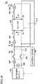
- FIG. 16 is a block diagram for illustrating an example configuration of a test system to test a power conversion device according to the third embodiment.
- a test system 5e corresponds to test system 5c (see FIG. 7 ) according to the first embodiment plus an inductance element 801 added to primary side DC terminal 1a of power conversion device 100 and an inductance element 802 added to secondary side output terminal 2a thereof.
- inductance elements 801 and 802 can be added by connecting inductors.
- inductance elements 801 and 802 may be added by parasitic inductances of power cables PL1 and PL2 that are "connection members.”
- inductance elements 801 and 802 can be added by intentionally increasing power cables PL1 and PL2 in length.
- an inductance element is added to at least a part of the group of DC terminals (1a, 1b, 2a, 2b) of a test target or power conversion device 100. That is, in other words, power conversion device 100 (a test target) is tested by supplying power from DC power supply 201 while an inductance element is added to at least a part of the group of DC terminals (1a, 1b, 2a, 2b) of power conversion device 100.
- power conversion device 100 can be tested in such a manner that the ripple current flows to the capacitor in power conversion device 100 rather than flowing out of power conversion device 100. As a result, accuracy of a test for evaluation of life for power conversion device 100 can be improved.
- inductance elements 801 and 802 are added to primary side DC terminal 1a and secondary side DC terminal 2a
- inductance element 801 may be added on the primary side to primary side DC terminal 1b.
- inductance element 802 may be added on the secondary side to secondary side DC terminal 2b.
- inductance element 801 or 802 can be added only to one of the primary side and the secondary side.
- an inductance element can also be added to at least one of primary side DC terminal 1a, 1b and secondary side DC terminal 2a, 2b in the test systems according to a modification of the first embodiment (see FIG. 10 ), the second embodiment (see FIG. 11 ) and a modification of the second embodiment (see FIG. 15 ), similarly as has been described with reference to FIG. 16 .
- the first to third embodiments and their modifications present configurations of power conversion device 100 and testing converter 400 by way of example and any circuit configuration therefor is applicable insofar as similar DC/DC conversion or AC/DC conversion is possible.
- connection member does not necessarily indicate an electric wire having a protective sheath on an insulated power supply; rather, it means a conductor that can pass a current.
- connection member When a bare conductor (for example, a bus bar) having a conductor uninsulated is used as the "connection member,” it is preferable to insulate it with an insulator or the like.
Landscapes
- Engineering & Computer Science (AREA)
- Power Engineering (AREA)
- Physics & Mathematics (AREA)
- General Physics & Mathematics (AREA)
- Inverter Devices (AREA)
- Dc-Dc Converters (AREA)
Abstract
Description
- The present invention relates to a system and method for testing a power conversion device, and more particularly to testing a power conversion device which performs direct current (DC) voltage conversion with an input and an output both being DC voltage.
- As a power conversion device for DC voltage conversion (hereinafter also referred to as "DC/DC conversion"), Patent Literature 1 (US Patent
US 5 027 264 A ) discloses that a configuration including two single- or three-phase full bridge circuits and a transformer is suitable for high power applications. Specifically, for the two full-bridge circuits, a DC terminal is connected to an input terminal or an output terminal of DC voltage, and an alternate current (AC) terminal is connected to a primary side winding or a secondary side winding of the transformer. This implements a power conversion device capable of DC/DC conversion with the primary side and the secondary side electrically insulated. Further,PTL 1 describes suppressing power loss by applying soft switching to semiconductor switching elements constituting each full bridge circuit. - PTL 1:
US 5 027 264 A - NPL 1: Rik W.A.A. De Doncker et. al., "A Three-Phase Soft-Switched High-Power-Density dc/dc Converter for High-Power Applications," IEEE TRANSACTIONS ON INDUSTRY APPLICATIONS, VOL. 27, NO. 1, JANUARY/FEBRUARY 1991.
- Testing a power conversion device, such as described in
PTL 1, requires a testing power supply and peripheral devices such as a protective circuit breaker and a measuring instrument. In particular, testing a power conversion device for high power applications entails a testing power supply and peripheral devices having increased rated capacities, and a test system increased in size and cost is a matter of concern. - The present invention has been made to solve such a problem, and an object of the present invention is to provide a system and method for efficiently testing a power conversion device which performs DC/DC conversion.
- According to an aspect of the present invention, a power conversion device test system includes at least one power conversion device which is a test target, a testing power supply for testing the test target, and first and second connection members. Each power conversion device performs DC voltage conversion between a primary side DC terminal and a secondary side DC terminal for inputting and outputting DC voltage. The first connection member connects the testing power supply and an input side of the test target. The second connection member electrically connects an output side of the test target and the testing power supply. Active power output from the output side of the test target is transmitted to the input side of the test target by the second connection member.
- According to another aspect of the present invention, a method for testing a power conversion device is a method in which at least one power conversion device is a test target, each power conversion device performing DC voltage conversion between a primary side DC terminal and a secondary side DC terminal for inputting and outputting DC voltage. When testing the test target, from the testing power supply electrically connected to the input side of the test target by the first connection member, the test target, with its input and output sides electrically connected via the second connection member, is supplied via the first connection member with active power smaller than active power which passes through the test target.
- According to the present invention, by supplying from a testing power supply active power smaller than active power passing through a power conversion device, which is a test target, the power conversion device can be efficiently tested.
-
- FIG. 1
- is a block diagram for illustrating a first example of a power conversion device which is a test target.
- FIG. 2
- is a circuit diagram for illustrating a first example configuration of a converter cell shown in
FIG. 1 . - FIG. 3
- is a circuit diagram for illustrating a second example configuration of the converter cell shown in
FIG. 1 . - FIG. 4
- is a block diagram for illustrating a second example of the power conversion device which is a test target.
- FIG. 5
- is a block diagram for illustrating a third example of the power conversion device which is a test target.
- FIG. 6
- is a block diagram for illustrating a fourth example of the power conversion device which is a test target.
- FIG. 7
- is a block diagram for illustrating an example configuration of a system to test a power conversion device according to a first embodiment.
- FIG. 8
- is a conceptual diagram for illustrating an operation of a converter cell shown in
FIG. 2 when a test is conducted. - FIG. 9
- is a conceptual diagram for illustrating an operation of a converter cell shown in
FIG. 3 when a test is conducted. - FIG. 10
- is a block diagram for illustrating an example configuration of a system to test a power conversion device according to a modification of the first embodiment.
- FIG. 11
- is a block diagram for illustrating an example configuration of a system to test a power conversion device according to a second embodiment.
- FIG. 12
- is a block diagram for illustrating an example configuration of a testing converter shown in
FIG. 11 . - FIG. 13
- is a circuit diagram for illustrating a first example configuration of a submodule shown in
FIG. 12 . - FIG. 14
- is a circuit diagram for illustrating a second example configuration of the submodule shown in
FIG. 12 . - FIG. 15
- is a block diagram for illustrating an example configuration of a system to test a power conversion device according to a modification of the second embodiment.
- FIG. 16
- is a block diagram for illustrating an example configuration of a system to test a power conversion device according to a third embodiment.
- Hereinafter, embodiments of the present invention will be described in detail with reference to the drawings. Hereinafter, identical or equivalent components in the figures are identically denoted and will not be described redundantly in principle.
- Initially, an example configuration of a power conversion device which is a test target in the present Embodiment will be described.
-
FIG. 1 is a block diagram for illustrating a first example of a power conversion device which is a test target. Referring toFIG. 1 , apower conversion device 100a according to the first example includes primaryside DC terminals side DC terminals converter cells 10.Converter cells 10 each perform DC/DC conversion. -
FIG. 2 is a circuit diagram for illustrating a first example configuration ofconverter cell 10 shown inFIG. 1 . Referring toFIG. 2 ,converter cell 10 according to the first example configuration includescapacitors phase transformer 8, afirst switching circuit 41, asecond switching circuit 42, and acontrol circuit 45.Control circuit 45 can be composed of dedicated hardware such as an analog circuit or an ASIC (Application Specific Integrated Circuit). Alternatively,control circuit 45 may have its functions partially or entirely implemented by software processing by a processor (not shown) executing a program installed in a memory (not shown). -
Transformer 8 includes a single-phase primary side winding 8x connected to primaryside AC nodes side AC nodes Capacitor 6 is connected between primaryside DC nodes Capacitor 7 is connected between secondaryside DC nodes - First switching
circuit 41 is connected between primaryside DC nodes side AC nodes circuit 41 includes semiconductor switching elements Q11 to Q14 connected in a single-phase full bridge, and freewheeling diodes D11 to D14 connected to semiconductor switching elements Q11 to Q14 in antiparallel. - Similarly,
second switching circuit 42 is connected between secondaryside DC nodes side AC nodes Second switching circuit 42 includes semiconductor switching elements Q21 to Q24 connected in a single-phase full bridge, and freewheeling diodes D21 to D24 connected to semiconductor switching elements Q21 to Q24 in antiparallel. - Semiconductor switching elements Q11 to Q14 and Q21 to Q24 can each be composed of a self arc-extinguishing switching element such as an IGBT (Insulated Gate Bipolar Transistor). Turning on/off semiconductor switching elements Q11 to Q14 and Q21 to Q24 can be controlled by control signals S11 to S14 and S21 to S24, respectively, issued from
control circuit 45. - Turning on/off semiconductor switching elements Q11 to Q14 is controlled so as to perform power conversion (DC/AC conversion) between DC voltage Vc1 of primary
side DC nodes side AC nodes side AC nodes side DC nodes - Thus,
converter cell 10 is configured as a so-called single-phase DAB (Dual-Active Bridge) that converts DC voltage to DC voltage via single-phase AC voltage transmitted via insulation bytransformer 8. First switchingcircuit 41 corresponds to an embodiment of a "first power conversion unit" andsecond switching circuit 42 corresponds to an embodiment of a "second power conversion unit." - In
converter cell 10 ofFIG. 2 , turning on/off semiconductor switching elements Q11 to Q14 and Q21 to Q24 can be controlled to control AC voltages V41 and V42 in amplitude and phase to control power transmission between the primary side and the secondary side in amount and direction, as desired. This is done in a known method, which is described for example inNPL 1. - Further, by outputs of temperature sensors (not shown) disposed at semiconductor switching elements Q11 to Q14 and Q21 to Q24 and freewheeling diodes D11 to D14 and D21 to D24,
control circuit 45 can detect temperatures TQ11 to TQ14 and TQ21 to TQ24 of semiconductor switching elements Q11 to Q14 and Q21 to Q24 and temperatures TD11 to TD14 and TD21 to TD24 of freewheeling diodes D11 to D14 and D21 to D24. Furthermore, disposing a voltage sensor (not shown) forcapacitors control circuit 45 to detect DC voltages Vc1 and Vc2. Similarly, disposing a current sensor (not shown) fortransformer 3 enablescontrol circuit 45 to also detect an AC current (single phase) passing throughtransformer 3. -
FIG. 3 shows a second example configuration ofconverter cell 10 shown inFIG. 1 . Referring toFIG. 3 ,converter cell 10 according to the second example configuration includes a three-phase transformer 3,capacitors first switching circuit 51, asecond switching circuit 52, and acontrol circuit 55. As well ascontrol circuit 45,control circuit 55 can also have its functions implemented by dedicated hardware and/or software processing by executing a program. -
Transformer 3 includes a three-phase primary side winding (not shown) connected to primaryside AC nodes side AC nodes Capacitor 6 is connected between primaryside DC nodes capacitor 7 is connected between secondaryside DC nodes FIG. 2 . - First switching
circuit 51 is connected between primaryside DC nodes side AC nodes circuit 51 includes semiconductor switching elements Q61 to Q66 connected in a three-phase full bridge, and freewheeling diodes D61 to D66 connected to semiconductor switching elements Q61 to Q66 in antiparallel. - Similarly,
second switching circuit 52 is connected between secondaryside DC nodes side AC nodes Second switching circuit 52 includes semiconductor switching elements Q71 to Q76 connected in a three-phase full bridge, and freewheeling diodes D71 to D76 connected to semiconductor switching elements Q71 to Q76 in antiparallel. - Semiconductor switching elements Q61 to Q66 and Q71 to Q76 can each also be composed of a self arc-extinguishing switching element such as an IGBT (Insulated Gate Bipolar Transistor). Turning on/off semiconductor switching elements Q61 to Q66 and Q71 to Q76 can be controlled by control signals S61 to S66 and S71 to S76, respectively, issued from
control circuit 55. - Turning on/off semiconductor switching elements Q61 to Q66 is controlled so as to perform power conversion (DC/AC conversion) between DC voltage Vc1 of primary
side DC nodes side AC nodes side AC nodes side DC nodes - Thus,
converter cell 10 is configured as a so-called 3-phase DAB (Dual-Active Bridge) that converts DC voltage to DC voltage via 3-phase AC voltage transmitted via insulation bytransformer 3. First switchingcircuit 51 corresponds to an embodiment of the "first power conversion unit," andsecond switching circuit 52 corresponds to an embodiment of the "second power conversion unit." - In
converter cell 10 ofFIG. 3 as well, turning on/off semiconductor switching elements Q61 to Q66 and Q71 to Q76 can be controlled to control 3-phase AC voltage in amplitude and phase to control power transmission between the primary side and the secondary side in amount and direction, as desired. This is done in a known method, which is described for example inNPL 1. - In the configuration of
FIG. 3 as well, by outputs of temperature sensors disposed at semiconductor switching elements Q61 to Q66, Q71 to Q76 and freewheeling diodes D61 to D66 and D71 to D76,control circuit 55 can detect temperatures TQ61 to TQ66 and TQ71 to TQ76 of semiconductor switching elements Q61 to Q66 and Q71 to Q76 and temperatures TD61 to TD66 and TD71 to TD76 of freewheeling diodes D61 to D66 and D71 to D76. It is also possible to dispose a voltage sensor (not shown) forcapacitors transformer 8. Thereby,control circuit 45 can further detect DC voltages Vc1 and Vc2 and an AC current (three phases) passing throughtransformer 8. - Referring to
FIG. 1 again, inpower conversion device 100a according to the first example, on the primary side, a plurality ofconverter cells 10 each have primaryside DC nodes side DC terminals power conversion device 100a, the plurality ofconverter cells 10 have secondaryside DC nodes side DC terminals - Thereby, in
power conversion device 100a, while power of a large current can be handled on the primary side, power of high voltage can be handled on the secondary side. Furthermore, DC power of low voltage can be converted to DC power of high voltage. -
FIG. 4 is a block diagram for illustrating a second example of a power conversion device which is a test target. Referring toFIG. 4 , apower conversion device 100b according to the second example is similar topower conversion device 100a, that is, it includes primaryside DC terminals side DC terminals converter cells 10. Inpower conversion device 100b, the plurality ofconverter cells 10 are connected in series on both the primary side and the secondary side. - Specifically, on the primary side of
power conversion device 100b, the plurality ofconverter cells 10 each have primaryside DC nodes side DC terminals power conversion device 100b as well, the plurality ofconverter cells 10 have secondaryside DC nodes side DC terminals transformers converter cell 10, inpower conversion device 100b, DC voltage between primaryside DC terminals side DC terminals -
FIG. 5 is a block diagram for illustrating a third example of a power conversion device which is a test target. Referring toFIG. 5 , apower conversion device 100c according to the third example is similar topower conversion devices side DC terminals side DC terminals converter cells 10. Inpower conversion device 100c, the plurality ofconverter cells 10 are connected in parallel on both the primary side and the secondary side. - Specifically, on the primary side of
power conversion device 100c, the plurality ofconverter cells 10 each have primaryside DC nodes side DC terminals power conversion device 100c as well, the plurality ofconverter cells 10 have secondaryside DC nodes side DC terminals transformers converter cell 10, inpower conversion device 100c as well, DC voltage between primaryside DC terminals side DC terminals -
FIG. 6 is a block diagram for illustrating a fourth example of a power conversion device which is a test target. Referring toFIG. 6 , apower conversion device 100d according to the third example is similar topower conversion devices 100a to 100c, that is, it includes primaryside DC terminals side DC terminals converter cells 10. - On the secondary side of
power conversion device 100d, as well aspower conversion device 100b (seeFIG. 4 ), the plurality ofconverter cells 10 have secondaryside DC nodes side DC terminals power conversion device 100d, every twoconverter cells 10 have primaryside DC nodes side DC nodes converter cells 10 that are connected in parallel are connected in series between primaryside DC terminals converter cells 10 are connected in series-parallel. - Thereby, on the primary side of
power conversion device 100d, intermediate DC voltage higher than the primary side of power converter (seeFIG. 5 ) 100c and lower thanpower conversion device 100b (seeFIG. 4 ) can be handled by using the same number ofconverter cells 10. And the intermediate DC voltage on the primary side can be converted on the secondary side to high voltage equivalent to that ofpower conversion device 100b. - In the present embodiment,
power conversion device 100 having a plurality ofconverter cells 10, includingpower conversion devices 100a to 100d described with reference to inFIGS. 1 and4 to 6 , are test targets. That is,power conversion device 100 includespower conversion devices 100a to 100d described above, and includes a plurality ofconverter cells 10 arranged in any number in any connection manner (series, parallel, or series-parallel). - In
power conversion device 100, depending on the number ofconverter cells 10 and how they are connected, DC voltage V1 between primaryside DC terminals side DC terminals FIGS. 4 and 5 , it is also possible to set V1 = V2. -
FIG. 7 is a block diagram for illustrating an example configuration of atest system 5a to test a power conversion device according to the first embodiment. - Referring to
FIG. 7 ,test system 5a testspower conversion device 100 with V1 = V2. In other words,power conversion device 100 shown inFIG. 7 is an embodiment of a "first power conversion device." -
Test system 5a includes aDC power supply 201 which is an example of the "testing power supply," atesting circuit breaker 205, measuringinstruments 206 to 209, power cables PL1 and PL2, and acontrol device 250. Inpower conversion device 100 which is the test target oftest system 5a, primaryside DC terminals side DC terminals - Power cable PL1 electrically connects
DC power supply 201 and primaryside DC terminals power conversion device 100. Power cable PL2 has one end connected to secondaryside DC terminals power conversion device 100 and the other end electrically connected to power cable PL1. Thereby, power cable PL2 electrically connects secondaryside DC terminals power conversion device 100 andDC power supply 201. That is, power cable PL1 corresponds to an embodiment of a "first connection member" and power cable PL2 corresponds to an embodiment of a "second connection member." -
Circuit breaker 205 is connected in series with power cable PL1.Circuit breaker 205 has a protective function to interrupt or form a current path in response to an open/close command received fromcontrol device 250 and automatically interrupt the current path when a value of a current exceeds a predetermined reference value. - Measuring
instrument 206 detects output voltage (power supply voltage) ofDC power supply 201. Measuringinstrument 207 measures an output current (a power supply current) ofDC power supply 201. Measuringinstrument 208 is connected to power cable PL1 and measures a current passing through primaryside DC terminals instrument 209 is connected to power cable PL2 and measures a current passing through secondaryside DC terminals instruments 206 to 209 are input to controldevice 250.Control circuit 250 can also have its functions configured by dedicated hardware such as an analog circuit, an ASIC or the like. Alternatively,control circuit 250 may be composed of a microcomputer or the like having a computing function and have its functions partially or entirely implemented by software processing by a processor (not shown) executing a program installed in a memory (not shown). - Further,
control device 250 can generate a command value forDC power supply 201, a command to open/close circuit breaker 205, and a command value forpower conversion device 100. Thereby, in testingpower conversion device 100, an output ofDC power supply 201, opening/closing circuit breaker 205, and an operation in power conversion device 100 (for example, turning on/off the semiconductor switching elements constituting converter cell 10) can be controlled. Further, a value detected inpower conversion device 100, e.g., a value in temperature detected in testing the semiconductor switching elements and the freewheeling diodes, as has been described with reference toFIGS. 3 and4 , can also be input to controldevice 250. - When testing
power conversion device 100 intest system 5a, power output from secondaryside DC terminals power conversion device 100 is transmitted to primaryside DC terminals power conversion device 100 through power cable PL2 to be a part of power input topower conversion device 100. Therefore, between active power Pi input to primaryside DC terminals power conversion device 100, active power Po output from secondaryside DC terminals power conversion device 100, and active power Ps supplied fromDC power supply 201, the following Equation (1) is established:
- From Equation (1), Ps = Pi - Po. Here, Pi - Po corresponds to power loss in
power conversion device 100, and it is understood that this power loss is equivalent to active power Ps supplied fromDC power supply 201. Active power Ps can be measured using measuringinstruments instruments instruments - Thus,
test system 5a according to the first embodiment can testpower conversion device 100 by supplying active power Ps smaller than active power Po passing throughpower conversion device 100. This allows a testing power supply (DC power supply 201),circuit breaker 205, and measuringinstrument 207 to have reduced rated capacities. As a result,test system 5a can be reduced in size and cost, andpower conversion device 100 can be efficiently tested. - Hereinafter, an operation of each
converter cell 10 in testingpower conversion device 100 will be described in detail. -
FIG. 8 is a conceptual diagram for illustrating an operation ofconverter cell 10 shown inFIG. 2 when a test is conducted.FIG. 8 shows an AC equivalent circuit of a single-phase DAB. - Referring to
FIG. 8 , anequivalent voltage source 410 is configured by turning on/off semiconductor switching elements Q11 to Q14 infirst switching circuit 41.Equivalent voltage source 410 outputs AC voltage (line voltage) V41 to primaryside AC nodes transformer 8, as has been shown inFIG. 2 . Similarly, anequivalent voltage source 420 is configured by turning on/off semiconductor switching elements Q21 to Q24 insecond switching circuit 42.Equivalent voltage source 420 outputs AC voltage (line voltage) V42 to secondaryside AC nodes transformer 8, as has been shown inFIG. 2 . -
Equivalent voltage sources equivalent inductance 80.Equivalent inductance 80 corresponds to leakage inductance oftransformer 8. Alternatively, when an inductor is additionally connected in series withtransformer 8, the inductance of the inductor is also included inequivalent inductance 80. - In the equivalent circuit of
FIG. 8 , line voltages V41 and 42 can be controlled in phase and amplitude, as desired, by controlling turning on/off semiconductor switching elements Q11 to Q14 infirst switching circuit 41 and semiconductor switching elements Q21 to Q24 insecond switching circuit 42. - By controlling a phase difference between line voltage V41 and line voltage V42, active power Pc passing through
converter cell 10 can be controlled. Accordingly, bycontrol circuit 45, control signals S11 to S14 and S21 to S24 can be generated to implement a switching pattern for semiconductor switching elements Q11 to Q14 and Q21 to Q24 for causing a phase difference following a command value for active power Pc. - Further, reactive power Qc generated in
converter cell 10 can be controlled by controlling an amplitude difference between line voltage V41 and line voltage V42. Accordingly, bycontrol circuit 45, control signals S11 to S14 and S21 to S24 can be generated to implement a switching pattern for semiconductor switching elements Q11 to Q14 and Q21 to Q24 for causing an amplitude difference following a command value for reactive power Qc. - Alternatively, control signals S11 to S14 and S21 to S24 can be generated to control a switching pattern for semiconductor switching elements Q11 to Q14 and Q21 to Q24 in accordance with a combination of the command value for active power Pc and the command value for reactive power Qc.
- In
test system 5a ofFIG. 7 ,capacitors first switching circuit 41 andsecond switching circuit 42 performs a zero voltage output operation. Specifically, in the zero voltage output operation, infirst switching circuit 41, while semiconductor switching elements Q11, Q13 (or Q12, Q14) are turned on, semiconductor switching elements Q12, Q14 (or Q11, Q13) are turned off to zero a voltage difference betweenAC nodes second switching circuit 42, in the zero voltage output operation, while semiconductor switching elements Q21 and Q23 (or Q22 and Q24) are turned on, semiconductor switching elements Q22 and Q24 (or Q21 and Q23) are turned off to zero a voltage difference between secondaryside AC nodes - Further, in the other of
first switching circuit 41 and second switching circuit 42 a normal operation for outputting AC voltage (single phase) controlled in phase and amplitude can be performed to cause an amplitude difference between line voltage V41 and line voltage V42. Thus, reactive power Qc can also be generated in eachconverter cell 10 when a test is conducted intest system 5a ofFIG. 7 . -
FIG. 9 is a conceptual diagram for illustrating an operation ofconverter cell 10 shown inFIG. 3 when a test is conducted.FIG. 9 shows an AC-side equivalent circuit of a three-phase DAB. - Referring to
FIG. 9 , anequivalent voltage source 510 is configured by turning on and off semiconductor switching elements Q61 to Q66 infirst switching circuit 51.Equivalent voltage source 510 outputs AC voltages (line voltages) V51a to V51c to primaryside AC nodes transformer 3, as has been shown inFIG. 2 . AC voltages (line voltages) V51a to V51c have a phase difference by 120 degrees. - Similarly, an
equivalent voltage source 520 is configured by turning on and off semiconductor switching elements Q71 to Q76 insecond switching circuit 52.Equivalent voltage source 520 outputs AC voltages (phase voltages) V52a to V52c to secondaryside AC nodes transformer 3, as shown inFIG. 2 . AC voltages (phase voltages) V52a to V52c have a phase difference by 120 degrees. -
Equivalent voltage sources equivalent inductance 30.Equivalent inductance 30 corresponds to leakage inductance oftransformer 3. Alternatively, when an inductor is additionally connected in series withtransformer 3, the inductance of the inductor is also included inequivalent inductance 30. - In the equivalent circuit of
FIG. 9 , phase voltages V51a to V51c can be controlled in phase and amplitude, as desired, by controlling turning on/off semiconductor switching elements Q61 to Q66 infirst switching circuit 51. Similarly, phase voltages V52a to V52c can be controlled in phase and amplitude, as desired, by controlling turning on/off semiconductor switching elements Q71 to Q76 insecond switching circuit 52. - In the 3-phase DAB circuit of
FIG. 3 as well, by controlling a phase difference of phase voltages V51a to V51c and phase voltages V52a to V52c, active power Pc passing throughconverter cell 10 can be controlled. Similarly, by controlling an amplitude difference of phase voltages V51a to V51c and phase voltages V52a to V52c, reactive power Qc passing throughconverter cell 10 can be controlled. - Accordingly, by
control circuit 55, control signals S61 to S66 and S71 to S76 can be generated to implement a switching pattern for semiconductor switching elements Q61 to Q66 and Q71 to Q76 for causing a phase difference and/or an amplitude difference following a command value for at least one of active power Pc and reactive power Qc. - Note that in
converter cell 10 ofFIG. 3 , whenfirst switching circuit 51 performs a zero voltage operation, while semiconductor switching elements Q61, Q63, Q65 (or Q62, Q64, Q66) are turned on, semiconductor switching elements Q62 Q64, Q66 (or Q61, Q63, Q65) are turned off to zero a voltage difference among primaryside AC nodes 31a to 31c. Similarly, whensecond switching circuit 52 performs a zero voltage output operation, while semiconductor switching elements Q71, Q73, Q75 (or Q72, Q74, Q76) are turned on, semiconductor switching elements Q72, Q74, Q76 (or Q71, Q73, Q75) are turned off to zero a voltage difference among secondaryside AC nodes 32a to 32c. - That is, in
test system 5a ofFIG. 7 , even whenpower conversion device 100a includingconverter cell 10 ofFIG. 3 is a test target, reactive power Qc can be generated in eachconverter cell 10 by performing a zero voltage output operation in one offirst switching circuit 51 andsecond switching circuit 52 and performing a normal operation in the other offirst switching circuit 51 andsecond switching circuit 52 for outputting AC voltage (three phases) controlled in phase and amplitude. - Referring to
FIG. 7 again, intest system 5a, controllability of active power ofpower conversion device 100 and power loss ofpower conversion device 100 can be measured by measuring active power Pi input to primaryside DC terminals side DC terminals DC power supply 201 as shown inFIG. 7 in a state in which active power Pc of eachconverter cell 10 is controlled in response to a command value issued fromcontrol device 250, as has been described with reference toFIGS. 8 and 9 . - Further, in
test system 5a, controllability ofpower conversion device 100 and whether an overcurrent is generated can be confirmed by measuring an AC current sensed by a current sensor disposed at transformer 3 (seeFIG. 2 ) or transformer 8 (seeFIG. 3 ). - Further, in
test system 5a, whether a balance of currents ofconverter cells 10 can also be confirmed by measuring currents of primaryside DC nodes side DC nodes converter cells 10. Further, whether a balance of voltages ofconverter cells 10 can also be confirmed by measuring the voltages ofcapacitors - Furthermore, in
test system 5a, by conducting a heat run test by measuring the temperature of the semiconductor switching elements and freewheeling diodes constituting eachconverter cell 10, it can be confirmed whether the temperature falls within a range lower than a tolerable value. For example, the tolerable value in the heat run test can be set to about 125 to 150°C. - In the heat run test, it is not a requirement to control active power, and it is possible to conduct the heat run test in a state with reactive power Qc controlled. Reactive power is power which is generated inside
power conversion device 100 and does not flow out ofpower conversion device 100. - Note that total power Pt passing through
power conversion device 100 corresponds to the square root of the sum of the square of active power Pc and the square of reactive power Qc (i.e., Pt = (Pc2 + Qc2)1/2). Therefore, according totest system 5a, active power Ps supplied from a testing power supply (DC power supply 201) is smaller than total power Pt passing throughpower conversion device 100. - That is, by generating reactive power, active power that testing
DC power supply 201 supplies can be reduced, so that the rated capacities of the testing power supply (DC power supply 201),circuit breaker 205, and measuringinstruments 207 to 209 can further be reduced, and the rated capacities of power cables PL1 and PL2 for connection for testing can also be reduced. - As described above, reactive power can be easily generated by controlling turning on/off the semiconductor switching elements in each
converter cell 10. As the reactive power is increased, the above effect is extended. For example, the reactive power in a test target orpower conversion device 100 can be made larger than the active power passing throughpower conversion device 100. -
FIG. 10 is a block diagram for illustrating an example configuration of atest system 5b to test a power conversion device according to a modification of the first embodiment. - Referring to
FIG. 10 , intest system 5b, twopower conversion devices 100 with V1 ≠ V2 are handled as a set as a test target. That is,power conversion device 100 shown inFIG. 10 is an embodiment of a "second power conversion device." - Note that in
FIG. 10 , it is assumed that V1 < V2. Further, in the following description, of the twopower conversion devices 100, one located on the left side inFIG. 10 will also be referred to as a preceding stage'spower conversion device 100, and the other one located on the right side inFIG. 10 will also be referred to as a following stage'spower conversion device 100. - Power cable PL1 electrically connects
DC power supply 201 and primaryside DC terminals power conversion device 100. Power cable PL2 has one end connected to secondaryside DC terminals power conversion device 100 and the other end electrically connected to power cable PL1. Power cable PL3 connects secondaryside DC terminals power conversion devices 100 that input and output DC voltage V2. - In
test system 5b ofFIG. 10 , primaryside DC terminals power conversion device 100 correspond to an input side of a test target, and primaryside DC terminals power conversion device 100 correspond to an output side of the test target. Therefore, intest system 5b as well, power cable PL1 corresponds to an embodiment of the "first connection member," and power cable PL2 corresponds to an embodiment of the "second connection member." -
Circuit breaker 205 and measuringinstruments test system 5a. For power cable PL1, a measuringinstrument 208 is further provided for measuring a current of primaryside DC terminals power conversion device 100. Furthermore, for power cable PL3, measuringinstruments instruments - Measurement values obtained by measuring
instruments 206 to 212 are input to controldevice 250. Active power Ps can be measured by measuringinstruments instruments instruments instruments - In addition to the function described for
test system 5a,control device 250 can generate a command value for each of the preceding and following stages'power conversion devices 100 for controlling an operation (i.e., power conversion). The command value includes the command values for active power Pc and reactive power Qc described in the first embodiment. In addition, the values of temperature, voltage, and a current sensed, as have been described in the first embodiment, can be obtained fromcontrol circuits power conversion device 100. - In
test system 5b, the preceding stage'spower conversion device 100 operates, as controlled, to increase DC voltage V1 input to primaryside DC terminals side DC terminals power conversion device 100 operates, as controlled, to decrease DC voltage V2 input to secondaryside DC terminals side DC terminals power conversion devices 100. - When
power conversion device 100 is tested intest system 5b, for active power Pi input from testingDC power supply 201 to primaryside DC terminals power conversion device 100, active power Pm is output from secondaryside DC terminals power conversion device 100 and input to secondaryside DC terminals power conversion device 100. Active power Po output from primaryside DC terminals power conversion device 100 is transmitted by power cable PL2 and will be a part of power input to the preceding stage'spower conversion device 100. - Therefore, active power Ps supplied from
AC power supply 301 will be Ps = Pi - Po. InFIG. 10 , Pi - Pm corresponds to power lost in the preceding stage'spower conversion device 100, and Pm - Po corresponds to power lost in the preceding stage'spower conversion device 100. Therefore, it is understood that active power Ps (Ps = Pi - Po) supplied fromDC power supply 201 is equivalent to power lost in both the preceding and following-stages'power conversion devices 100. - Thus,
test system 5b according to a modification of the first embodiment can test a power conversion device by supplying active power Ps smaller than active power Po passing through a test target which ispower conversion device 100 having different input and output voltages. This allows a testing power supply (DC power supply 201),circuit breaker 205, and measuringinstrument 207 to have reduced rated capacities. As a result,test system 5b can be reduced in size and cost, andpower conversion device 100 having different input and output voltages can be efficiently tested. - Furthermore, the preceding stage's
power conversion device 100 in a configuration in which primaryside DC terminals test system 5b can further be reduced in size and cost by reducing an insulating member in size. - The test conducted at each
power conversion device 100 has specific contents which are similar to those in the first embodiment, including a heat run test and generation of reactive power, and accordingly, will not be described repeatedly in detail. - Further, in
test system 5b, a power conversion operation in the preceding stage'spower conversion device 100 in a direction in which primaryside DC terminals side DC terminals power conversion device 100 in a direction in which secondaryside DC terminals side DC terminals - Further, of the two
power conversion devices 100, the preceding stage'spower conversion device 100 can control DC voltage V2 of secondaryside DC terminals power conversion device 100 can control active power Po. Alternatively, while the following stage'spower conversion device 100 can control DC voltage V2 of secondaryside DC terminals power conversion device 100 can control active power Pm. Thus, in a test of a power conversion device usingtest system 5b, it is also possible to simultaneously verify controllability of output voltage and controllability of output power (or active power) (e.g., control accuracy and control responsiveness) for a test target which is twopower conversion devices 100. - In the second embodiment, a test system using an AC power supply as a testing power supply will be described.
-
FIG. 11 is a block diagram for illustrating an example configuration of atest system 5c to test a power conversion device according to the second embodiment. - Referring to
FIG. 11 ,test system 5c includesAC power supply 301,testing circuit breaker 305, measuringinstruments testing converters control device 350.Control circuit 350, as well ascontrol circuit 250, can also have its functions configured by dedicated hardware such as an analog circuit, an ASIC or the like. Alternatively,control circuit 350 may be composed of a microcomputer or the like having a computing function and have its functions partially or entirely implemented by software processing by a processor (not shown) executing a program installed in a memory (not shown). -
AC power supply 301 can be configured by a power supply device having a controllable output or an AC power system (for example, 6.6 kV).Testing converter 400a performs AC/DC conversion between AC voltage ofAC power supply 301 and DC voltage V1 of primaryside DC terminals power conversion device 100.Testing converter 400b performs DC/AC conversion between DC voltage V2 of secondaryside DC terminals power conversion device 100 and AC voltage ofAC power supply 301. -
FIG. 12 shows an example configuration oftesting converters FIG. 11 .Testing converters testing converter 400. - Referring to
FIG. 12 ,testing converter 400 can be constituted by a modular multilevel converter which performs AC/DC power conversion or DC/AC power conversion bidirectionally betweenAC nodes DC nodes - In the modular multilevel converter, for each phase (U, V, W) of AC voltage, an
arm circuit 430 in which a plurality ofsubmodules 50 and a reactor are connected in series is arranged on each of a positive side and a negative side. In the example ofFIG. 12 , threearm circuits 430 for U, V, and W phases (for the positive side) are connected betweenAC nodes DC node 407x. Similarly, threearm circuits 430 for U, V, and W phases (for the negative side) are connected betweenAC nodes DC node 407y. In eacharm circuit 430, a plurality ofsubmodules 50 haveoutput terminals -
FIG. 13 shows a first example configuration ofsubmodule 50 shown inFIG. 12 . Referring toFIG. 13 ,submodule 50 according to the first example configuration has a so-called half-bridge configuration. Specifically,submodule 50 includes a pair ofoutput terminals Output terminal output terminal submodule 50,AC node DC node FIG. 12 . - Capacitor Ca is connected between node Nx and node Ny, semiconductor switching element Q91 is electrically connected between
output terminal 408x and node Nx, and semiconductor switching element Q92 is electrically connected betweenoutput terminals - In
submodule 50 ofFIG. 13 , capacitor Ca is connected betweenoutput terminals output terminals -
FIG. 14 shows a second example configuration ofsubmodule 50 shown inFIG. 12 . Referring toFIG. 14 ,submodule 50 according to the second example configuration has a so-called full bridge configuration. Specifically,submodule 50 includes a pair ofoutput terminals Output terminal output terminal submodule 50,AC node DC node - Capacitor Ca is connected between nodes Nx and Ny. Semiconductor switching element Q91 is electrically connected between node Nx and
output terminal 408x, and semiconductor switching element Q92 is electrically connected betweenoutput terminal 408x and node Ny. Similarly, semiconductor switching element Q93 is electrically connected between node Nx andoutput terminal 408y, and semiconductor switching element Q94 is electrically connected betweenoutput terminal 408y and node Ny. Freewheeling diodes D91 to D94 are connected to semiconductor switching elements Q91 to Q94 in antiparallel. - In
submodule 50 ofFIG. 13 , capacitor Ca is connected tooutput terminals output terminals - Referring to
FIG. 12 again, in eacharm circuit 430, output voltage betweenoutput terminals submodules 50 is controlled by turning on and off the semiconductor switching elements. As a result, in the modular multilevel converter, the above-described AC/DC conversion or DC/AC conversion can be performed bidirectionally between DC voltage ofDC nodes AC nodes DC nodes - Referring to
FIG. 11 again,testing converter 400a hasDC nodes FIG. 12 ) electrically connected to primaryside DC terminals power conversion device 100 via power cable PL1.Testing converter 400b hasDC nodes FIG. 12 ) electrically connected to secondaryside DC terminals power conversion device 100 via power cable PL2. -
AC power supply 301 is electrically connected toAC nodes FIG. 12 ) oftesting converter 400a by power cable PL10.Testing converter 400b hasAC nodes AC power supply 301 via power cables PL11 and PL10. Note thattesting converters AC nodes -
Circuit breaker 305 and measuringinstrument 306 are connected to power cablePL10. Circuit breaker 305 has a protective function to interrupt or form a current path in response to an open/close command received fromcontrol device 350 and automatically interrupt the current path when a value of a current exceeds a predetermined reference value. Measuringinstrument 306 measures active power Ps supplied fromAC power supply 301. - Measuring
instrument 307 for measuring AC power input/output to/fromtesting converter 400a is connected to power cable PL10. Similarly, measuringinstrument 308 for measuring AC power input/output to/fromtesting converter 400b is connected to power cable PL11. Measuringinstruments instruments device 350. - Furthermore,
control device 350 can generate a command to open/close circuit breaker 305, a command value forpower conversion device 100, and a command value for testing converters (or modular multilevel converters) 400a and 400b. Thereby, in testingpower conversion device 100, opening/closing circuit breaker 305, an operation in power conversion device 100 (for example, turning on/off the semiconductor switching elements constituting converter cell 10), and output voltage oftesting converters - For example,
control device 350 generates a command value fortesting converter 400a that is connected to primaryside DC terminals control device 350 generates a command value fortesting converter 400b that is connected to secondaryside DC terminals - Further, similarly as done for
control device 250 of the first embodiment, a value sensed inpower conversion device 100, e.g., a value in temperature sensed of the semiconductor switching elements and the freewheeling diodes when a test is conducted, as has been described with reference toFIGS. 3 and4 , can be input to controldevice 350. - In
power conversion device 100 which is a test target oftest system 5c, primaryside DC terminals side DC terminals testing converters test system 5c may be either a power conversion device with V1 = V2 (the first power conversion device) orpower conversion devices 100 with V1 ≠ V2 (the second power converter). - When testing
power conversion device 100 intest system 5c, by controlling active power ofpower conversion device 100 in response to a command value issued fromcontrol device 350, while active power Pi is input to primaryside DC terminals side DC terminals control device 350,testing converter 400a performs AC/DC conversion so as to control power cable PL1 at DC voltage VI, andtesting converter 400b performs DC/AC conversion so as to control power cable PL2 at DC voltage V2. - As a result, active power Pf is generated on the AC side of
testing converter 400a (or on power cable PL 10), and active power Pb is generated on the AC side oftesting converter 400b (or on power cable PL11). - Active power Pb on the AC side of
testing converter 400b will be a part of active power Pf on the AC side oftesting converter 400a. That is, active power Po output from secondaryside DC terminals power conversion device 100 is transmitted by power cables PL2 and PL11 through power conversion bytesting converters side DC terminals power conversion device 100 and becomes a part of active power Pi input topower conversion device 100. - Therefore, active power Ps supplied from
AC power supply 301 will be Ps = Pf - Pb. Pf - Pi corresponds to loss intesting converter 400a, Po - Pf corresponds to loss intesting converter 400b, and Po - Pi corresponds to loss inpower conversion device 100, and accordingly, it is understood that power Ps corresponds to total loss intesting converters power conversion device 100. - Thus,
test system 5c according to the second embodiment can testpower conversion device 100 by supplying active power Ps smaller than active power Po passing throughpower conversion device 100. This allows a testing power supply (AC power supply 301),circuit breaker 305, and measuringinstrument 306 to have reduced rated capacities. As a result,test system 5c can be reduced in size and cost, andpower conversion device 100 can be efficiently tested even when an AC power supply (including a power supply system) is used as a testing power supply. - Note that in the example configuration of
FIG. 11 , power cables PL10 and PL1 correspond to an embodiment of the "first connection member," and power cables PL11 and PL2 correspond to an embodiment of the "second connection member." Further,testing converter 400a corresponds to a "first testing converter," andtesting converter 400b corresponds to a "second testing converter." - The test conducted at
power conversion device 100 has specific contents which are similar to those in the first embodiment, including a heat run test and generation of reactive power, and accordingly, will not be described repeatedly in detail.Test system 5c according to the second embodiment also allows a heat run test to be conducted with reactive power Qc passed. In particular, by generating reactive power Qc inpower conversion device 100, the rated power oftesting converters AC power supply 301 but also testingconverters - Note that while an example has been described in which in
test system 5c, while testingconverters power conversion device 100 controls active powers Po and Pi, this manner of sharing control is changeable. For example, one oftesting converters power conversion device 100. In that case, the other oftesting converters power conversion device 100 can be evaluated. - Alternatively, in
test system 5c, a behavior when DC-side voltage ofpower conversion device 100 rapidly decreases can be evaluated by rapidly decreasing DC voltage thattesting converter - While
test system 5c according to the second embodiment can test bothpower conversion device 100 with V1 = V2 andpower conversion device 100 with V1 ≠ V2, twotesting converters power conversion device 100 with V1 = V2 will be described. -
FIG. 15 is a block diagram for illustrating an example configuration of atest system 5d to test a power conversion device according to a modification of the second embodiment. - Referring to
FIG. 15 ,test system 5d includesAC power supply 301,testing circuit breaker 305, measuringinstruments testing converter 400a, power cables PL1, PL2, PL10, andcontrol device 350. Further, inpower conversion device 100 that is a test target, DC voltage V1 of primaryside DC terminals side DC terminals - When
test system 5d is compared withtest system 5c according to the second embodiment (seeFIG. 11 ),test system 5d differs in thattesting converter 400b and power cable PL11 are dispensed with. Furthermore, power cable PL2 is electrically connected between secondaryside DC terminals power conversion device 100 and power cable PL1, as in the first embodiment and a modification thereof (seeFIGS. 7 and10 ).Test system 5d has a remainder in configuration similar to that oftest system 5c according to the second embodiment, and accordingly, will not be described repeatedly in detail. - Power cable PL2 electrically connects secondary
side DC terminals power conversion device 100 toAC power supply 301 via power cables PL1 and PL10 andtesting converter 400a. That is, in the example configuration ofFIG. 15 , power cable PL1 corresponds to an embodiment of the "first connection member," and power cable PL2 corresponds to an embodiment of a "second connection member." - In
test system 5d, active power Po output from secondaryside DC terminals power conversion device 100 is transmitted to primaryside DC terminals power conversion device 100 by power cable PL2 and becomes a part of active power Pi input topower conversion device 100. - Furthermore, active power Ps supplied from
AC power supply 301 is equal to active power Pf on the AC side oftesting converter 400a, and Pf - Pi corresponds to loss oftesting converter 400a. As a result, it is understood that active power Ps corresponds to a total of loss intesting converter 400a andpower conversion device 100. - Thus,
test system 5d according to a modification of the second embodiment can testpower conversion device 100 by supplying active power Ps smaller than active power Po passing throughpower conversion device 100. As a result, a testing power supply (AC power supply 301),circuit breaker 305, and measuringinstrument 306 can have reduced rated capacities, andtest system 5d can be reduced in size and cost. - Furthermore, when compared with
test system 5c, a smaller number of testing converters can be disposed, so that in a configuration using an AC power supply (including a power supply system) as a testing power supply, a test system specialized forpower conversion device 100 with V1 = V2 can further be reduced in size. - In
test system 5d as well, the test conducted atpower conversion device 100 has specific contents which are similar to those in the first embodiment, including a heat run test and generation of reactive power, and accordingly, will not be described repeatedly in detail. Further, while inFIG. 15 power conversion device 100 with DC voltages V1 and V2 being equivalent (the first power conversion device) is indicated as a test target by way of example, intest system 5d two power conversion devices with DC voltages V1 and V2 being different (the second power conversion device) connected similarly as shown inFIG. 10 (a modification of the first embodiment) can also be a test target. - In a third embodiment will be described a test system and a test method according the first and second embodiments and their modifications with an inductance element added to a DC terminal of a test target, or a power conversion device.
-
FIG. 16 is a block diagram for illustrating an example configuration of a test system to test a power conversion device according to the third embodiment. - Referring to
FIG. 16 , atest system 5e according to the third
embodiment corresponds to testsystem 5c (seeFIG. 7 ) according to the first embodiment plus aninductance element 801 added to primary side DC terminal 1a ofpower conversion device 100 and aninductance element 802 added to secondaryside output terminal 2a thereof. Typically,inductance elements inductance elements inductance elements - When a ripple current is generated by a switching operation of
power conversion device 100, the ripple current should flow tocapacitors 6 and 7 (FIG. 2 ) present insidepower conversion device 100, and therefore does not flow out ofpower conversion device 100. However, when an inductance component outer than the group of DC terminals (1a, 1b, 2a, 2b) ofpower conversion device 100 is small, the above capacitor's filtering effect is not sufficiently exhibited, and the ripple current may flow out ofpower conversion device 100 through the group of DC terminals (1a, 1b, 2a, 2b). - When the ripple current flows to the capacitor, power loss occurs in the capacitor, and the temperature of the capacitor rises. Since heat generation in the capacitor significantly affects the life of
power conversion device 100, it is necessary to evaluate it by a test. If the ripple current flows out ofpower conversion device 100, as described above, during a test, what effect the ripple current has in the capacitor inpower conversion device 100 cannot be correctly tested, and a correct lifetime evaluation forpower conversion device 100 may no longer be performed. - In a test system according to the third embodiment, an inductance element is added to at least a part of the group of DC terminals (1a, 1b, 2a, 2b) of a test target or
power conversion device 100. That is, in other words, power conversion device 100 (a test target) is tested by supplying power fromDC power supply 201 while an inductance element is added to at least a part of the group of DC terminals (1a, 1b, 2a, 2b) ofpower conversion device 100. - Thus,
power conversion device 100 can be tested in such a manner that the ripple current flows to the capacitor inpower conversion device 100 rather than flowing out ofpower conversion device 100. As a result, accuracy of a test for evaluation of life forpower conversion device 100 can be improved. - While in
FIG. 16 inductance elements side DC terminal 1a and secondaryside DC terminal 2a,inductance element 801 may be added on the primary side to primaryside DC terminal 1b. Similarly,inductance element 802 may be added on the secondary side to secondaryside DC terminal 2b. Alternatively,inductance element - While in
FIG. 16 an example configuration in which an inductance element is added to testsystem 5a (seeFIG. 7 ) according to the first embodiment has been described, an inductance element can also be added to at least one of primaryside DC terminal side DC terminal FIG. 10 ), the second embodiment (seeFIG. 11 ) and a modification of the second embodiment (seeFIG. 15 ), similarly as has been described with reference toFIG. 16 . - The first to third embodiments and their modifications present configurations of
power conversion device 100 andtesting converter 400 by way of example and any circuit configuration therefor is applicable insofar as similar DC/DC conversion or AC/DC conversion is possible. - While the first to third embodiments and their modifications present a power cable as an embodiment of a "connection member," a connection member other than the power cable is applicable insofar as it ensures electrical connection. That is, the "connection member" does not necessarily indicate an electric wire having a protective sheath on an insulated power supply; rather, it means a conductor that can pass a current. When a bare conductor (for example, a bus bar) having a conductor uninsulated is used as the "connection member," it is preferable to insulate it with an insulator or the like.
- The embodiments disclosed herein are also planned to be combined together as appropriate for implementation. It should be understood that the embodiments disclosed herein have been described for the purpose of illustration only and in a non-restrictive manner in any respect. The scope of the present invention is defined by the terms of the claims, rather than the embodiments description above, and is intended to include any modifications within the meaning and scope equivalent to the terms of the claims.
-
- 1a, 1b
- primary side DC terminal
- 2a, 2b
- secondary side DC terminal
- 3, 8
- transformer
- 5a-5d
- test system
- 6, 7, Ca
- capacitor
- 8x
- primary side winding
- 8y
- secondary side winding
- 10
- converter cell
- 11a, 11b
- primary side DC node (power conversion device)
- 12a, 12b
- secondary side DC node (power conversion device)
- 30, 80
- equivalent inductance
- 31a-31c
- primary side AC node
- 81a, 81b
- primary side AC node
- 32a-32c
- secondary side AC node
- 82a, 82b
- secondary side AC node
- 41, 51
- first switching circuit
- 42, 52
- second switching circuit
- 45, 55
- control circuit
- 50
- submodule
- 100
- power conversion device
- 100a-100d
- power conversion device
- 201
- DC power supply
- 205, 305
- circuit breaker
- 206-212
- measuring instrument
- 306-308
- measuring instrument
- 250, 350
- control device
- 301 AC
- power supply
- 400
- testing converter
- 400a, 400b
- testing converter
- 406u
- AC node (MMC)
- 406v, 406w
- AC node (MMC)
- 407x, 407y
- DC node (MMC)
- 408x, 408y
- output terminal (MMC)
- 410, 420
- equivalent voltage source
- 510, 520
- equivalent voltage source
- 430
- arm circuit (MMC)
- 801, 802
- inductance element
- D11-D14
- freewheeling diode
- D21-D24
- freewheeling diode
- D61-D66
- freewheeling diode
- D71-D76
- freewheeling diode
- D91-D94
- freewheeling diode
- Nx, Ny
- node
- Pb, Pc, Pf
- active power
- Pi, Pm
- active power
- Po, Ps
- active power
- PL1-PL3
- power cable
- PL10, PL11
- power cable
- Q11-Q14
- semiconductor switching element
- Q21-Q24
- semiconductor switching element
- Q61-Q66
- semiconductor switching element
- Q71-Q76
- semiconductor switching element
- Q91-Q94
- semiconductor switching element
- Qc
- reactive power
- S11-S14
- control signal (semiconductor switching element)
- S21-S24
- control signal (semiconductor switching element)
- S61-S66
- control signal (semiconductor switching element)
- S71-S76
- control signal (semiconductor switching element).
Claims (22)
- A system to test a power conversion device, comprising:at least one power conversion device to serve as a test target,each power conversion device to perform DC voltage conversion between a primary side DC terminal and a secondary side DC terminal for inputting and outputting DC voltage;a testing power supply for the test target;a first connection member to electrically connect the testing power supply and an input side of the test target; anda second connection member to electrically connect an output side of the test target and the testing power supply for transmitting active power output from the output side of the test target to the input side of the test target.
- The system to test a power conversion device according to claim 1,
wherein
the test target is a first power conversion device with the DC voltage being equivalent between the primary side DC terminal and the secondary side DC terminal,
the first connection member electrically connects the testing power supply and the primary side DC terminal, and
the second connection member electrically connects the secondary side DC terminal and the first connection member. - The system to test a power conversion device according to claim 1,
wherein
the test target includes two second power conversion devices with the DC voltage being different between the primary side DC terminal and the secondary side DC terminal,
the two second power conversion devices have their respective secondary DC terminals electrically connected to each other,
the first connection member electrically connects the primary side DC terminal of one of the two second power conversion devices and the testing power supply, and
the second connection member electrically connects the primary side DC terminal of the other of the two second power conversion devices and the first connection member. - The system to test a power conversion device according to claim 3,
wherein the DC voltage of the primary side DC terminal is lower than the DC voltage of the secondary side DC terminal. - The system to test a power conversion device
according to any one of claims 1 to 4,
wherein the testing power supply includes a DC power supply. - The system to test a power conversion device according to claim 1, the testing power supply including an AC power supply, the system further comprising:a first testing converter electrically connected between the AC power supply and the primary side DC terminal via the first connection member to perform AC/DC voltage conversion between a first AC node electrically connected to the AC power supply and a first DC node electrically connected to the primary side DC terminal; anda second testing converter electrically connected between the AC power supply and the secondary side DC terminal via the second connection member to perform DC/AC voltage conversion between a second DC node electrically connected to the secondary side DC terminal and a second AC node electrically connected to the AC power supply.
- The system to test a power conversion device according to claim 1,
the test target including a first power conversion device with the DC voltage equivalent between the primary side DC terminal and the secondary side DC terminal or two second power conversion devices with the DC voltage different between the primary side DC terminal and the secondary side DC terminal, the testing power supply including an AC power supply, the system further comprising a testing converter electrically connected between the AC power supply and the primary side DC terminal via the first connection member to perform AC/DC voltage conversion between an AC node electrically connected to the AC power supply and a DC node electrically connected to the primary side DC terminal, wherein
the first connection member electrically connects the DC node and the primary side DC terminal, and
the second connection member electrically connects the secondary side DC terminal and the first connection member. - The system to test a power conversion device according to claim 6 or 7, wherein each testing converter is a modular multilevel converter having a plurality of submodules.
- The system to test a power conversion device
according to any one of claims 1 to 8,
wherein each power conversion device includes a plurality of converter cells, the plurality of converter cells each includinga primary side DC node electrically connected to the primary side DC terminal,a secondary side DC node electrically connected to the secondary side DC terminal,a transformer having a primary side winding and a secondary side winding,a first power conversion unit connected between the primary side DC node and the primary side winding,a first capacitor connected to the primary side DC node,a second power conversion unit connected between the secondary side DC node and the secondary side winding, anda second capacitor connected to the secondary side DC node, andthe first and second power conversion units each perform power conversion between DC voltage and AC voltage by controlling turning on/off a plurality of semiconductor switching elements. - The system to test a power conversion device according to claim 9,
wherein the plurality of semiconductor switching elements are controlled so that in each power conversion device, reactive power generated by AC voltage is larger than active power passing through the power conversion device. - The system to test a power conversion device
according to any one of claims 1 to 10,
further comprising an inductance element added to at least one of the primary side DC terminal and the secondary side DC terminal of each power conversion device. - A method for testing a power conversion device, at least one power conversion device being a test target in the method, wherein
the power conversion device performs DC voltage conversion between a primary side DC terminal and a secondary side DC terminal for inputting and outputting DC voltage, and
when the test target is tested, from a testing power supply electrically connected to an input side of the test target by a first connection member, the test target, with an output side of the test target and the input side electrically connected via a second connection member, is supplied via the first connection member with active power smaller than active power passing through the test target. - The method for testing a power conversion device according to claim 12,
wherein
the test target is a first power conversion device with the DC voltage being equivalent between the primary side DC terminal and the secondary side DC terminal, and
when the test target is tested, the first power conversion device receives power from the testing power supply while the testing power supply and the primary side DC terminal are electrically connected by the first connection member and the secondary side DC terminal and the first connection member are electrically connected by the second connection member. - The method for testing a power conversion device according to claim 12,
wherein
the test target includes two second power conversion devices with the DC voltage being different between the primary side DC terminal and the secondary side DC terminal,
the two second power conversion devices have their respective secondary DC terminals electrically connected to each other,
the first connection member electrically connects the primary side DC terminal of one of the two second power conversion devices and the testing power supply, and
when the test target is tested, the two second power conversion devices receive power from the testing power supply while the primary side DC terminal of the other of the two second power conversion devices and the first connection member are electrically connected by the second connection member. - The method for testing a power conversion device according to claim 14, wherein the DC voltage of the primary side DC terminal is lower than the DC voltage of the secondary side DC terminal.
- The method for testing a power conversion device
according to any one of claims 12 to 15,
wherein the testing power supply includes a DC power supply. - The method for testing a power conversion device according to claim 12,
wherein the testing power supply includes an AC power supply,
when the test target is tested, AC/DC voltage conversion is performed between AC voltage of the AC power supply and DC voltage of the primary side DC terminal by a first testing converter electrically connected between the AC power supply and the primary side DC terminal via the first connection member andDC/AC voltage conversion is performed between DC voltage of the secondary side DC terminal and AC voltage of the AC power supply by a second testing converter electrically connected between the AC power supply and the secondary side DC terminal via the second connection member, andthe power conversion device receives power from the testing power supply while the primary side DC terminal and the secondary side DC terminal are electrically connected via the first and second connection members. - The method for testing a power conversion device according to claim 12,
wherein
the test target includes a first power conversion device with the DC voltage equivalent between the primary side DC terminal and the secondary side DC terminal or two second power conversion devices with the DC voltage different between the primary side DC terminal and the secondary side DC terminal,
the testing power supply includes an AC power supply,
when the test target is tested, AC/DC voltage conversion is performed between AC voltage of the AC power supply and DC voltage of the primary side DC terminal by a testing converter electrically connected between the AC power supply and the primary side DC terminal via the first connection member, and
the first power conversion device receives power from the testing power supply while the primary side DC terminal and the secondary side DC terminal are electrically connected via the first and second connection members. - The method for testing a power conversion device according to claim 17 or 18, wherein each testing converter is a modular multilevel converter having a plurality of submodules.
- The method for testing a power conversion device
according to any one of claims 12 to 19,
wherein the power conversion device includes a plurality of converter cells, the plurality of converter cells each includinga primary side DC node electrically connected to the primary side DC terminal,a secondary side DC node electrically connected to the secondary side DC terminal,a transformer having a primary side winding and a secondary side winding,a first power conversion unit connected between the primary side DC node and the primary side winding,a first capacitor connected to the primary side DC node,a second power conversion unit connected between the secondary side DC node and the secondary side winding, anda second capacitor connected to the secondary side DC node, and the first and second power conversion units each perform power conversion between DC voltage and AC voltage by controlling turning on/off a plurality of semiconductor switching elements. - The method for testing a power conversion device according to claim 20,
wherein in testing the test target, the plurality of semiconductor switching elements are controlled so that in each power conversion device, reactive power generated by AC voltage is larger than active power passing through the power conversion device. - The method for testing a power conversion device according to any one of claims 12 to 21,
wherein when the test target is tested the test target receives power from the testing power supply via the first connection member with an inductance element added to at least one of the primary side DC terminal and the secondary side DC terminal of each power conversion device.
Applications Claiming Priority (2)
| Application Number | Priority Date | Filing Date | Title |
|---|---|---|---|
| JP2017217083 | 2017-11-10 | ||
| PCT/JP2018/022164 WO2019092911A1 (en) | 2017-11-10 | 2018-06-11 | Test system and test method for power conversion device |
Publications (3)
| Publication Number | Publication Date |
|---|---|
| EP3709493A1 true EP3709493A1 (en) | 2020-09-16 |
| EP3709493A4 EP3709493A4 (en) | 2020-12-23 |
| EP3709493B1 EP3709493B1 (en) | 2023-12-13 |
Family
ID=66438791
Family Applications (1)
| Application Number | Title | Priority Date | Filing Date |
|---|---|---|---|
| EP18877150.5A Active EP3709493B1 (en) | 2017-11-10 | 2018-06-11 | Test system and test method for power conversion device |
Country Status (4)
| Country | Link |
|---|---|
| US (1) | US11428748B2 (en) |
| EP (1) | EP3709493B1 (en) |
| JP (1) | JP6456578B1 (en) |
| WO (1) | WO2019092911A1 (en) |
Families Citing this family (9)
| Publication number | Priority date | Publication date | Assignee | Title |
|---|---|---|---|---|
| WO2019146399A1 (en) * | 2018-01-25 | 2019-08-01 | 三菱電機株式会社 | Capacitor testing device, electric power conversion device and capacitor testing method |
| CN111404370A (en) * | 2020-03-05 | 2020-07-10 | 北京动力源新能源科技有限责任公司 | A kind of DC-DC power module testing equipment and using method |
| JP2021158703A (en) * | 2020-03-25 | 2021-10-07 | 株式会社日立製作所 | Bidirectional DC-DC converter |
| CN113552509B (en) * | 2020-04-24 | 2024-10-22 | 南京南瑞继保电气有限公司 | A kind of operation test circuit of power electronic transformer module and its starting method |
| JP7567282B2 (en) * | 2020-08-24 | 2024-10-16 | 株式会社プロテリアル | Test methods for isolated converters |
| CN115684757B (en) * | 2021-07-31 | 2024-04-09 | 宁德时代新能源科技股份有限公司 | Test system and method for power conversion device, electronic equipment and storage medium |
| US12176813B2 (en) | 2021-08-23 | 2024-12-24 | Infineon Technologies Austria Ag | Trans-inductance multi-phase power converters, monitoring and management |
| JP7786209B2 (en) * | 2022-01-12 | 2025-12-16 | 株式会社明電舎 | DAB bidirectional isolated DC/DC converter and its control method |
| US20250314712A1 (en) * | 2024-04-09 | 2025-10-09 | George Burcea | System to test power supplies with reduced thermal dissipation |
Family Cites Families (18)
| Publication number | Priority date | Publication date | Assignee | Title |
|---|---|---|---|---|
| JPH0633428Y2 (en) * | 1988-04-30 | 1994-08-31 | 株式会社計測技術研究所 | DC power aging device |
| US5027264A (en) | 1989-09-29 | 1991-06-25 | Wisconsin Alumni Research Foundation | Power conversion apparatus for DC/DC conversion using dual active bridges |
| JP2000241477A (en) | 1999-02-18 | 2000-09-08 | Shindengen Electric Mfg Co Ltd | Operation method for direct current power supply device to be tested |
| AUPQ113799A0 (en) * | 1999-06-22 | 1999-07-15 | University Of Queensland, The | A method and device for measuring lymphoedema |
| JP4235936B2 (en) | 2002-05-17 | 2009-03-11 | Tdkラムダ株式会社 | Power supply aging test equipment |
| JP4242619B2 (en) * | 2002-09-09 | 2009-03-25 | 東芝三菱電機産業システム株式会社 | Test method for self-excited transducer |
| US6775160B2 (en) * | 2002-09-27 | 2004-08-10 | The Aerospace Corporation | Dynamic DC source and load energy recycling power system |
| EP2341594A1 (en) | 2009-12-29 | 2011-07-06 | Converteam Technology Ltd | Power collection and transmission systems |
| HK1147389A2 (en) | 2010-06-04 | 2011-08-05 | 黄汉基 | A power supply burn-in system |
| CN101902127A (en) * | 2010-06-11 | 2010-12-01 | 刘军 | Electronic load energy recovery scheme based on DC bus |
| DE112015006097T5 (en) | 2015-02-02 | 2017-11-30 | Mitsubishi Electric Corporation | DC / DC CONVERTER |
| JP6572150B2 (en) | 2016-02-09 | 2019-09-04 | 株式会社東芝 | Power converter |
| CN105811460B (en) | 2016-05-04 | 2019-10-25 | 中车株洲电力机车研究所有限公司 | A kind of power module high frequency test system for electronic power transformer |
| EP3905507A4 (en) * | 2018-12-25 | 2021-12-15 | Mitsubishi Electric Corporation | POWER CONVERSION DEVICE |
| US12021440B2 (en) * | 2019-01-21 | 2024-06-25 | Mitsubishi Electric Corporation | Power conversion device and DC power distribution system |
| JP6605186B1 (en) * | 2019-05-10 | 2019-11-13 | 三菱電機株式会社 | DC power distribution system |
| WO2021044485A1 (en) * | 2019-09-02 | 2021-03-11 | 東芝三菱電機産業システム株式会社 | Testing device for inverter apparatus |
| CN112362989B (en) * | 2020-10-30 | 2021-11-02 | 湖北工业大学 | High-voltage electrostatic precipitator spark discharge simulation device and test method |
-
2018
- 2018-06-11 JP JP2018553255A patent/JP6456578B1/en active Active
- 2018-06-11 US US16/649,798 patent/US11428748B2/en active Active
- 2018-06-11 WO PCT/JP2018/022164 patent/WO2019092911A1/en not_active Ceased
- 2018-06-11 EP EP18877150.5A patent/EP3709493B1/en active Active
Also Published As
| Publication number | Publication date |
|---|---|
| JPWO2019092911A1 (en) | 2019-11-14 |
| EP3709493B1 (en) | 2023-12-13 |
| EP3709493A4 (en) | 2020-12-23 |
| US11428748B2 (en) | 2022-08-30 |
| WO2019092911A1 (en) | 2019-05-16 |
| JP6456578B1 (en) | 2019-01-23 |
| US20200264239A1 (en) | 2020-08-20 |
Similar Documents
| Publication | Publication Date | Title |
|---|---|---|
| EP3709493B1 (en) | Test system and test method for power conversion device | |
| Barker et al. | A current flow controller for use in HVDC grids | |
| US20150003134A1 (en) | Modular multilevel converter using asymmetry | |
| Sastry et al. | Considerations for the design of power electronic modules for hybrid distribution transformers | |
| US20110019449A1 (en) | Power converter apparatus | |
| EP3288169B1 (en) | Power conversion device | |
| EP2471164B1 (en) | Converter cell module with autotransformer bypass, voltage source converter system comprising such a module and a method for controlling such a system | |
| EP2983284A1 (en) | Power conversion device | |
| US20170338654A1 (en) | Modular multi-level converter with thyristor valves | |
| US20180212533A1 (en) | A multilevel converter with reduced ac fault handling rating | |
| US11228255B2 (en) | Rectifier assembly | |
| CA2623157A1 (en) | Method for controlling a polyphase converter with distributed energy stores | |
| EP3926812A1 (en) | Power conversion device and power conversion system | |
| EP3826165B1 (en) | Improvements in or relating to power dissipating converters | |
| WO2021205801A1 (en) | Dc power distribution system | |
| US10554120B2 (en) | Power conversion device | |
| KR20130124228A (en) | Power supply system with a first and a second power supply equipments | |
| KR101886804B1 (en) | Apparatus and method for testing operation of modular multi-level converter | |
| WO2018163582A1 (en) | Power conversion device | |
| WO2015004120A2 (en) | Dc to dc converter assembly | |
| RU2012147667A (en) | METHOD FOR MATCHING A HETEROGENEOUS FOUR WIRE NONSymmetric ELECTRIC TRANSMISSION LINE WITH ELECTRIC LOAD | |
| GB2519762A (en) | DC to DC converter assembly | |
| JP7387078B1 (en) | power converter | |
| CN110050318B (en) | switchgear | |
| CN114982120A (en) | Improvements in or relating to chain-link modules for voltage source converters |
Legal Events
| Date | Code | Title | Description |
|---|---|---|---|
| STAA | Information on the status of an ep patent application or granted ep patent |
Free format text: STATUS: THE INTERNATIONAL PUBLICATION HAS BEEN MADE |
|
| PUAI | Public reference made under article 153(3) epc to a published international application that has entered the european phase |
Free format text: ORIGINAL CODE: 0009012 |
|
| STAA | Information on the status of an ep patent application or granted ep patent |
Free format text: STATUS: REQUEST FOR EXAMINATION WAS MADE |
|
| 17P | Request for examination filed |
Effective date: 20200505 |
|
| AK | Designated contracting states |
Kind code of ref document: A1 Designated state(s): AL AT BE BG CH CY CZ DE DK EE ES FI FR GB GR HR HU IE IS IT LI LT LU LV MC MK MT NL NO PL PT RO RS SE SI SK SM TR |
|
| AX | Request for extension of the european patent |
Extension state: BA ME |
|
| A4 | Supplementary search report drawn up and despatched |
Effective date: 20201124 |
|
| RIC1 | Information provided on ipc code assigned before grant |
Ipc: G01R 31/40 20200101ALI20201118BHEP Ipc: H02M 3/28 20060101AFI20201118BHEP |
|
| DAV | Request for validation of the european patent (deleted) | ||
| DAX | Request for extension of the european patent (deleted) | ||
| GRAP | Despatch of communication of intention to grant a patent |
Free format text: ORIGINAL CODE: EPIDOSNIGR1 |
|
| STAA | Information on the status of an ep patent application or granted ep patent |
Free format text: STATUS: GRANT OF PATENT IS INTENDED |
|
| INTG | Intention to grant announced |
Effective date: 20230626 |
|
| GRAS | Grant fee paid |
Free format text: ORIGINAL CODE: EPIDOSNIGR3 |
|
| GRAA | (expected) grant |
Free format text: ORIGINAL CODE: 0009210 |
|
| STAA | Information on the status of an ep patent application or granted ep patent |
Free format text: STATUS: THE PATENT HAS BEEN GRANTED |
|
| P01 | Opt-out of the competence of the unified patent court (upc) registered |
Effective date: 20231005 |
|
| AK | Designated contracting states |
Kind code of ref document: B1 Designated state(s): AL AT BE BG CH CY CZ DE DK EE ES FI FR GB GR HR HU IE IS IT LI LT LU LV MC MK MT NL NO PL PT RO RS SE SI SK SM TR |
|
| REG | Reference to a national code |
Ref country code: GB Ref legal event code: FG4D |
|
| REG | Reference to a national code |
Ref country code: CH Ref legal event code: EP |
|
| REG | Reference to a national code |
Ref country code: DE Ref legal event code: R096 Ref document number: 602018062752 Country of ref document: DE |
|
| REG | Reference to a national code |
Ref country code: IE Ref legal event code: FG4D |
|
| REG | Reference to a national code |
Ref country code: SE Ref legal event code: TRGR |
|
| PG25 | Lapsed in a contracting state [announced via postgrant information from national office to epo] |
Ref country code: GR Free format text: LAPSE BECAUSE OF FAILURE TO SUBMIT A TRANSLATION OF THE DESCRIPTION OR TO PAY THE FEE WITHIN THE PRESCRIBED TIME-LIMIT Effective date: 20240314 |
|
| REG | Reference to a national code |
Ref country code: LT Ref legal event code: MG9D |
|
| PG25 | Lapsed in a contracting state [announced via postgrant information from national office to epo] |
Ref country code: LT Free format text: LAPSE BECAUSE OF FAILURE TO SUBMIT A TRANSLATION OF THE DESCRIPTION OR TO PAY THE FEE WITHIN THE PRESCRIBED TIME-LIMIT Effective date: 20231213 |
|
| REG | Reference to a national code |
Ref country code: NL Ref legal event code: MP Effective date: 20231213 |
|
| PG25 | Lapsed in a contracting state [announced via postgrant information from national office to epo] |
Ref country code: ES Free format text: LAPSE BECAUSE OF FAILURE TO SUBMIT A TRANSLATION OF THE DESCRIPTION OR TO PAY THE FEE WITHIN THE PRESCRIBED TIME-LIMIT Effective date: 20231213 |
|
| PG25 | Lapsed in a contracting state [announced via postgrant information from national office to epo] |
Ref country code: LT Free format text: LAPSE BECAUSE OF FAILURE TO SUBMIT A TRANSLATION OF THE DESCRIPTION OR TO PAY THE FEE WITHIN THE PRESCRIBED TIME-LIMIT Effective date: 20231213 Ref country code: GR Free format text: LAPSE BECAUSE OF FAILURE TO SUBMIT A TRANSLATION OF THE DESCRIPTION OR TO PAY THE FEE WITHIN THE PRESCRIBED TIME-LIMIT Effective date: 20240314 Ref country code: ES Free format text: LAPSE BECAUSE OF FAILURE TO SUBMIT A TRANSLATION OF THE DESCRIPTION OR TO PAY THE FEE WITHIN THE PRESCRIBED TIME-LIMIT Effective date: 20231213 Ref country code: BG Free format text: LAPSE BECAUSE OF FAILURE TO SUBMIT A TRANSLATION OF THE DESCRIPTION OR TO PAY THE FEE WITHIN THE PRESCRIBED TIME-LIMIT Effective date: 20240313 |
|
| REG | Reference to a national code |
Ref country code: AT Ref legal event code: MK05 Ref document number: 1641325 Country of ref document: AT Kind code of ref document: T Effective date: 20231213 |
|
| PG25 | Lapsed in a contracting state [announced via postgrant information from national office to epo] |
Ref country code: NL Free format text: LAPSE BECAUSE OF FAILURE TO SUBMIT A TRANSLATION OF THE DESCRIPTION OR TO PAY THE FEE WITHIN THE PRESCRIBED TIME-LIMIT Effective date: 20231213 |
|
| PG25 | Lapsed in a contracting state [announced via postgrant information from national office to epo] |
Ref country code: RS Free format text: LAPSE BECAUSE OF FAILURE TO SUBMIT A TRANSLATION OF THE DESCRIPTION OR TO PAY THE FEE WITHIN THE PRESCRIBED TIME-LIMIT Effective date: 20231213 Ref country code: NO Free format text: LAPSE BECAUSE OF FAILURE TO SUBMIT A TRANSLATION OF THE DESCRIPTION OR TO PAY THE FEE WITHIN THE PRESCRIBED TIME-LIMIT Effective date: 20240313 Ref country code: NL Free format text: LAPSE BECAUSE OF FAILURE TO SUBMIT A TRANSLATION OF THE DESCRIPTION OR TO PAY THE FEE WITHIN THE PRESCRIBED TIME-LIMIT Effective date: 20231213 Ref country code: LV Free format text: LAPSE BECAUSE OF FAILURE TO SUBMIT A TRANSLATION OF THE DESCRIPTION OR TO PAY THE FEE WITHIN THE PRESCRIBED TIME-LIMIT Effective date: 20231213 Ref country code: HR Free format text: LAPSE BECAUSE OF FAILURE TO SUBMIT A TRANSLATION OF THE DESCRIPTION OR TO PAY THE FEE WITHIN THE PRESCRIBED TIME-LIMIT Effective date: 20231213 |
|
| PG25 | Lapsed in a contracting state [announced via postgrant information from national office to epo] |
Ref country code: IS Free format text: LAPSE BECAUSE OF FAILURE TO SUBMIT A TRANSLATION OF THE DESCRIPTION OR TO PAY THE FEE WITHIN THE PRESCRIBED TIME-LIMIT Effective date: 20240413 |
|
| PG25 | Lapsed in a contracting state [announced via postgrant information from national office to epo] |
Ref country code: CZ Free format text: LAPSE BECAUSE OF FAILURE TO SUBMIT A TRANSLATION OF THE DESCRIPTION OR TO PAY THE FEE WITHIN THE PRESCRIBED TIME-LIMIT Effective date: 20231213 Ref country code: AT Free format text: LAPSE BECAUSE OF FAILURE TO SUBMIT A TRANSLATION OF THE DESCRIPTION OR TO PAY THE FEE WITHIN THE PRESCRIBED TIME-LIMIT Effective date: 20231213 |
|
| PG25 | Lapsed in a contracting state [announced via postgrant information from national office to epo] |
Ref country code: SK Free format text: LAPSE BECAUSE OF FAILURE TO SUBMIT A TRANSLATION OF THE DESCRIPTION OR TO PAY THE FEE WITHIN THE PRESCRIBED TIME-LIMIT Effective date: 20231213 |
|
| PG25 | Lapsed in a contracting state [announced via postgrant information from national office to epo] |
Ref country code: SM Free format text: LAPSE BECAUSE OF FAILURE TO SUBMIT A TRANSLATION OF THE DESCRIPTION OR TO PAY THE FEE WITHIN THE PRESCRIBED TIME-LIMIT Effective date: 20231213 Ref country code: SK Free format text: LAPSE BECAUSE OF FAILURE TO SUBMIT A TRANSLATION OF THE DESCRIPTION OR TO PAY THE FEE WITHIN THE PRESCRIBED TIME-LIMIT Effective date: 20231213 Ref country code: RO Free format text: LAPSE BECAUSE OF FAILURE TO SUBMIT A TRANSLATION OF THE DESCRIPTION OR TO PAY THE FEE WITHIN THE PRESCRIBED TIME-LIMIT Effective date: 20231213 Ref country code: IT Free format text: LAPSE BECAUSE OF FAILURE TO SUBMIT A TRANSLATION OF THE DESCRIPTION OR TO PAY THE FEE WITHIN THE PRESCRIBED TIME-LIMIT Effective date: 20231213 Ref country code: IS Free format text: LAPSE BECAUSE OF FAILURE TO SUBMIT A TRANSLATION OF THE DESCRIPTION OR TO PAY THE FEE WITHIN THE PRESCRIBED TIME-LIMIT Effective date: 20240413 Ref country code: EE Free format text: LAPSE BECAUSE OF FAILURE TO SUBMIT A TRANSLATION OF THE DESCRIPTION OR TO PAY THE FEE WITHIN THE PRESCRIBED TIME-LIMIT Effective date: 20231213 Ref country code: CZ Free format text: LAPSE BECAUSE OF FAILURE TO SUBMIT A TRANSLATION OF THE DESCRIPTION OR TO PAY THE FEE WITHIN THE PRESCRIBED TIME-LIMIT Effective date: 20231213 Ref country code: AT Free format text: LAPSE BECAUSE OF FAILURE TO SUBMIT A TRANSLATION OF THE DESCRIPTION OR TO PAY THE FEE WITHIN THE PRESCRIBED TIME-LIMIT Effective date: 20231213 |
|
| PG25 | Lapsed in a contracting state [announced via postgrant information from national office to epo] |
Ref country code: PT Free format text: LAPSE BECAUSE OF FAILURE TO SUBMIT A TRANSLATION OF THE DESCRIPTION OR TO PAY THE FEE WITHIN THE PRESCRIBED TIME-LIMIT Effective date: 20240415 Ref country code: PL Free format text: LAPSE BECAUSE OF FAILURE TO SUBMIT A TRANSLATION OF THE DESCRIPTION OR TO PAY THE FEE WITHIN THE PRESCRIBED TIME-LIMIT Effective date: 20231213 |
|
| PG25 | Lapsed in a contracting state [announced via postgrant information from national office to epo] |
Ref country code: PT Free format text: LAPSE BECAUSE OF FAILURE TO SUBMIT A TRANSLATION OF THE DESCRIPTION OR TO PAY THE FEE WITHIN THE PRESCRIBED TIME-LIMIT Effective date: 20240415 Ref country code: PL Free format text: LAPSE BECAUSE OF FAILURE TO SUBMIT A TRANSLATION OF THE DESCRIPTION OR TO PAY THE FEE WITHIN THE PRESCRIBED TIME-LIMIT Effective date: 20231213 |
|
| REG | Reference to a national code |
Ref country code: DE Ref legal event code: R097 Ref document number: 602018062752 Country of ref document: DE |
|
| PG25 | Lapsed in a contracting state [announced via postgrant information from national office to epo] |
Ref country code: DK Free format text: LAPSE BECAUSE OF FAILURE TO SUBMIT A TRANSLATION OF THE DESCRIPTION OR TO PAY THE FEE WITHIN THE PRESCRIBED TIME-LIMIT Effective date: 20231213 |
|
| PLBE | No opposition filed within time limit |
Free format text: ORIGINAL CODE: 0009261 |
|
| STAA | Information on the status of an ep patent application or granted ep patent |
Free format text: STATUS: NO OPPOSITION FILED WITHIN TIME LIMIT |
|
| PG25 | Lapsed in a contracting state [announced via postgrant information from national office to epo] |
Ref country code: SI Free format text: LAPSE BECAUSE OF FAILURE TO SUBMIT A TRANSLATION OF THE DESCRIPTION OR TO PAY THE FEE WITHIN THE PRESCRIBED TIME-LIMIT Effective date: 20231213 |
|
| PG25 | Lapsed in a contracting state [announced via postgrant information from national office to epo] |
Ref country code: SI Free format text: LAPSE BECAUSE OF FAILURE TO SUBMIT A TRANSLATION OF THE DESCRIPTION OR TO PAY THE FEE WITHIN THE PRESCRIBED TIME-LIMIT Effective date: 20231213 Ref country code: DK Free format text: LAPSE BECAUSE OF FAILURE TO SUBMIT A TRANSLATION OF THE DESCRIPTION OR TO PAY THE FEE WITHIN THE PRESCRIBED TIME-LIMIT Effective date: 20231213 |
|
| 26N | No opposition filed |
Effective date: 20240916 |
|
| PG25 | Lapsed in a contracting state [announced via postgrant information from national office to epo] |
Ref country code: MC Free format text: LAPSE BECAUSE OF FAILURE TO SUBMIT A TRANSLATION OF THE DESCRIPTION OR TO PAY THE FEE WITHIN THE PRESCRIBED TIME-LIMIT Effective date: 20231213 |
|
| REG | Reference to a national code |
Ref country code: CH Ref legal event code: PL |
|
| PG25 | Lapsed in a contracting state [announced via postgrant information from national office to epo] |
Ref country code: LU Free format text: LAPSE BECAUSE OF NON-PAYMENT OF DUE FEES Effective date: 20240611 |
|
| PG25 | Lapsed in a contracting state [announced via postgrant information from national office to epo] |
Ref country code: IE Free format text: LAPSE BECAUSE OF NON-PAYMENT OF DUE FEES Effective date: 20240611 |
|
| PG25 | Lapsed in a contracting state [announced via postgrant information from national office to epo] |
Ref country code: CH Free format text: LAPSE BECAUSE OF NON-PAYMENT OF DUE FEES Effective date: 20240630 Ref country code: BE Free format text: LAPSE BECAUSE OF NON-PAYMENT OF DUE FEES Effective date: 20240630 |
|
| REG | Reference to a national code |
Ref country code: BE Ref legal event code: MM Effective date: 20240630 |
|
| PGFP | Annual fee paid to national office [announced via postgrant information from national office to epo] |
Ref country code: DE Payment date: 20250429 Year of fee payment: 8 |
|
| PGFP | Annual fee paid to national office [announced via postgrant information from national office to epo] |
Ref country code: GB Payment date: 20250501 Year of fee payment: 8 |
|
| PGFP | Annual fee paid to national office [announced via postgrant information from national office to epo] |
Ref country code: FR Payment date: 20250508 Year of fee payment: 8 |
|
| PGFP | Annual fee paid to national office [announced via postgrant information from national office to epo] |
Ref country code: SE Payment date: 20250429 Year of fee payment: 8 |
|
| PG25 | Lapsed in a contracting state [announced via postgrant information from national office to epo] |
Ref country code: FI Free format text: LAPSE BECAUSE OF FAILURE TO SUBMIT A TRANSLATION OF THE DESCRIPTION OR TO PAY THE FEE WITHIN THE PRESCRIBED TIME-LIMIT Effective date: 20231213 |
|
| PG25 | Lapsed in a contracting state [announced via postgrant information from national office to epo] |
Ref country code: CY Free format text: LAPSE BECAUSE OF FAILURE TO SUBMIT A TRANSLATION OF THE DESCRIPTION OR TO PAY THE FEE WITHIN THE PRESCRIBED TIME-LIMIT; INVALID AB INITIO Effective date: 20180611 |
|
| PG25 | Lapsed in a contracting state [announced via postgrant information from national office to epo] |
Ref country code: HU Free format text: LAPSE BECAUSE OF FAILURE TO SUBMIT A TRANSLATION OF THE DESCRIPTION OR TO PAY THE FEE WITHIN THE PRESCRIBED TIME-LIMIT; INVALID AB INITIO Effective date: 20180611 |