EP3709359A1 - Solid-state imaging device and electronic device - Google Patents
Solid-state imaging device and electronic device Download PDFInfo
- Publication number
- EP3709359A1 EP3709359A1 EP18875891.6A EP18875891A EP3709359A1 EP 3709359 A1 EP3709359 A1 EP 3709359A1 EP 18875891 A EP18875891 A EP 18875891A EP 3709359 A1 EP3709359 A1 EP 3709359A1
- Authority
- EP
- European Patent Office
- Prior art keywords
- pixel
- section
- trench
- dti
- photoelectric conversion
- Prior art date
- Legal status (The legal status is an assumption and is not a legal conclusion. Google has not performed a legal analysis and makes no representation as to the accuracy of the status listed.)
- Pending
Links
- 238000003384 imaging method Methods 0.000 title claims abstract description 129
- 239000000758 substrate Substances 0.000 claims abstract description 140
- 238000006243 chemical reaction Methods 0.000 claims abstract description 110
- 239000004065 semiconductor Substances 0.000 claims abstract description 45
- 238000009792 diffusion process Methods 0.000 claims description 210
- 238000012546 transfer Methods 0.000 claims description 152
- 230000000149 penetrating effect Effects 0.000 claims description 45
- 239000000463 material Substances 0.000 claims description 28
- 229920006395 saturated elastomer Polymers 0.000 claims description 25
- 238000002955 isolation Methods 0.000 claims description 7
- 238000005516 engineering process Methods 0.000 abstract description 151
- 230000006866 deterioration Effects 0.000 abstract description 26
- 239000010410 layer Substances 0.000 description 241
- 239000007790 solid phase Substances 0.000 description 130
- 230000000694 effects Effects 0.000 description 72
- 238000000034 method Methods 0.000 description 47
- VYPSYNLAJGMNEJ-UHFFFAOYSA-N Silicium dioxide Chemical compound O=[Si]=O VYPSYNLAJGMNEJ-UHFFFAOYSA-N 0.000 description 44
- 230000005684 electric field Effects 0.000 description 43
- 230000001965 increasing effect Effects 0.000 description 43
- 239000012535 impurity Substances 0.000 description 39
- 230000008569 process Effects 0.000 description 35
- 229910052681 coesite Inorganic materials 0.000 description 23
- 229910052906 cristobalite Inorganic materials 0.000 description 23
- 229910052682 stishovite Inorganic materials 0.000 description 23
- 229910052905 tridymite Inorganic materials 0.000 description 23
- 230000015572 biosynthetic process Effects 0.000 description 22
- 230000000875 corresponding effect Effects 0.000 description 21
- 238000001514 detection method Methods 0.000 description 21
- 230000002093 peripheral effect Effects 0.000 description 21
- 239000000377 silicon dioxide Substances 0.000 description 21
- 235000012239 silicon dioxide Nutrition 0.000 description 21
- 230000006870 function Effects 0.000 description 19
- 229910021420 polycrystalline silicon Inorganic materials 0.000 description 19
- 229920005591 polysilicon Polymers 0.000 description 19
- 230000002829 reductive effect Effects 0.000 description 17
- 238000010586 diagram Methods 0.000 description 16
- 239000002775 capsule Substances 0.000 description 15
- 239000000945 filler Substances 0.000 description 15
- 239000007769 metal material Substances 0.000 description 14
- 238000012545 processing Methods 0.000 description 14
- 238000002598 diffusion tensor imaging Methods 0.000 description 12
- 238000004891 communication Methods 0.000 description 10
- WFKWXMTUELFFGS-UHFFFAOYSA-N tungsten Chemical compound [W] WFKWXMTUELFFGS-UHFFFAOYSA-N 0.000 description 10
- 229910052721 tungsten Inorganic materials 0.000 description 10
- 239000010937 tungsten Substances 0.000 description 10
- 238000004519 manufacturing process Methods 0.000 description 9
- 239000003990 capacitor Substances 0.000 description 8
- 229910052782 aluminium Inorganic materials 0.000 description 7
- XAGFODPZIPBFFR-UHFFFAOYSA-N aluminium Chemical compound [Al] XAGFODPZIPBFFR-UHFFFAOYSA-N 0.000 description 7
- 239000004020 conductor Substances 0.000 description 7
- 229910052751 metal Inorganic materials 0.000 description 7
- 239000002184 metal Substances 0.000 description 7
- 230000002441 reversible effect Effects 0.000 description 7
- IJGRMHOSHXDMSA-UHFFFAOYSA-N Atomic nitrogen Chemical compound N#N IJGRMHOSHXDMSA-UHFFFAOYSA-N 0.000 description 6
- XUIMIQQOPSSXEZ-UHFFFAOYSA-N Silicon Chemical compound [Si] XUIMIQQOPSSXEZ-UHFFFAOYSA-N 0.000 description 6
- 230000005540 biological transmission Effects 0.000 description 6
- 238000000605 extraction Methods 0.000 description 6
- 229910052710 silicon Inorganic materials 0.000 description 6
- 239000010703 silicon Substances 0.000 description 6
- 229910052581 Si3N4 Inorganic materials 0.000 description 5
- 238000009825 accumulation Methods 0.000 description 5
- 238000005468 ion implantation Methods 0.000 description 5
- 230000035945 sensitivity Effects 0.000 description 5
- HQVNEWCFYHHQES-UHFFFAOYSA-N silicon nitride Chemical compound N12[Si]34N5[Si]62N3[Si]51N64 HQVNEWCFYHHQES-UHFFFAOYSA-N 0.000 description 5
- 241000519995 Stachys sylvatica Species 0.000 description 4
- 229910000420 cerium oxide Inorganic materials 0.000 description 4
- 229910003440 dysprosium oxide Inorganic materials 0.000 description 4
- NLQFUUYNQFMIJW-UHFFFAOYSA-N dysprosium(iii) oxide Chemical compound O=[Dy]O[Dy]=O NLQFUUYNQFMIJW-UHFFFAOYSA-N 0.000 description 4
- 229910001940 europium oxide Inorganic materials 0.000 description 4
- AEBZCFFCDTZXHP-UHFFFAOYSA-N europium(3+);oxygen(2-) Chemical compound [O-2].[O-2].[O-2].[Eu+3].[Eu+3] AEBZCFFCDTZXHP-UHFFFAOYSA-N 0.000 description 4
- 238000010438 heat treatment Methods 0.000 description 4
- 229910003443 lutetium oxide Inorganic materials 0.000 description 4
- 230000007246 mechanism Effects 0.000 description 4
- 230000003287 optical effect Effects 0.000 description 4
- BMMGVYCKOGBVEV-UHFFFAOYSA-N oxo(oxoceriooxy)cerium Chemical compound [Ce]=O.O=[Ce]=O BMMGVYCKOGBVEV-UHFFFAOYSA-N 0.000 description 4
- MPARYNQUYZOBJM-UHFFFAOYSA-N oxo(oxolutetiooxy)lutetium Chemical compound O=[Lu]O[Lu]=O MPARYNQUYZOBJM-UHFFFAOYSA-N 0.000 description 4
- SIWVEOZUMHYXCS-UHFFFAOYSA-N oxo(oxoyttriooxy)yttrium Chemical compound O=[Y]O[Y]=O SIWVEOZUMHYXCS-UHFFFAOYSA-N 0.000 description 4
- RVTZCBVAJQQJTK-UHFFFAOYSA-N oxygen(2-);zirconium(4+) Chemical compound [O-2].[O-2].[Zr+4] RVTZCBVAJQQJTK-UHFFFAOYSA-N 0.000 description 4
- 238000009751 slip forming Methods 0.000 description 4
- 229910001928 zirconium oxide Inorganic materials 0.000 description 4
- ZOXJGFHDIHLPTG-UHFFFAOYSA-N Boron Chemical compound [B] ZOXJGFHDIHLPTG-UHFFFAOYSA-N 0.000 description 3
- OAICVXFJPJFONN-UHFFFAOYSA-N Phosphorus Chemical compound [P] OAICVXFJPJFONN-UHFFFAOYSA-N 0.000 description 3
- 229910052796 boron Inorganic materials 0.000 description 3
- 238000013500 data storage Methods 0.000 description 3
- 230000002708 enhancing effect Effects 0.000 description 3
- 238000005530 etching Methods 0.000 description 3
- 239000011159 matrix material Substances 0.000 description 3
- 238000002156 mixing Methods 0.000 description 3
- 238000012986 modification Methods 0.000 description 3
- 230000004048 modification Effects 0.000 description 3
- 229910052757 nitrogen Inorganic materials 0.000 description 3
- TWNQGVIAIRXVLR-UHFFFAOYSA-N oxo(oxoalumanyloxy)alumane Chemical compound O=[Al]O[Al]=O TWNQGVIAIRXVLR-UHFFFAOYSA-N 0.000 description 3
- BPUBBGLMJRNUCC-UHFFFAOYSA-N oxygen(2-);tantalum(5+) Chemical compound [O-2].[O-2].[O-2].[O-2].[O-2].[Ta+5].[Ta+5] BPUBBGLMJRNUCC-UHFFFAOYSA-N 0.000 description 3
- 229910052698 phosphorus Inorganic materials 0.000 description 3
- 239000011574 phosphorus Substances 0.000 description 3
- 230000001681 protective effect Effects 0.000 description 3
- 239000010936 titanium Substances 0.000 description 3
- GWEVSGVZZGPLCZ-UHFFFAOYSA-N Titan oxide Chemical compound O=[Ti]=O GWEVSGVZZGPLCZ-UHFFFAOYSA-N 0.000 description 2
- RTAQQCXQSZGOHL-UHFFFAOYSA-N Titanium Chemical compound [Ti] RTAQQCXQSZGOHL-UHFFFAOYSA-N 0.000 description 2
- NRTOMJZYCJJWKI-UHFFFAOYSA-N Titanium nitride Chemical compound [Ti]#N NRTOMJZYCJJWKI-UHFFFAOYSA-N 0.000 description 2
- UPEMFLOMQVFMCZ-UHFFFAOYSA-N [O--].[O--].[O--].[Pm+3].[Pm+3] Chemical compound [O--].[O--].[O--].[Pm+3].[Pm+3] UPEMFLOMQVFMCZ-UHFFFAOYSA-N 0.000 description 2
- 239000000654 additive Substances 0.000 description 2
- 230000000996 additive effect Effects 0.000 description 2
- 238000000231 atomic layer deposition Methods 0.000 description 2
- 230000001276 controlling effect Effects 0.000 description 2
- 230000002596 correlated effect Effects 0.000 description 2
- 230000003247 decreasing effect Effects 0.000 description 2
- 230000007547 defect Effects 0.000 description 2
- 238000005401 electroluminescence Methods 0.000 description 2
- 238000007667 floating Methods 0.000 description 2
- CMIHHWBVHJVIGI-UHFFFAOYSA-N gadolinium(iii) oxide Chemical compound [O-2].[O-2].[O-2].[Gd+3].[Gd+3] CMIHHWBVHJVIGI-UHFFFAOYSA-N 0.000 description 2
- 229910052735 hafnium Inorganic materials 0.000 description 2
- CJNBYAVZURUTKZ-UHFFFAOYSA-N hafnium(iv) oxide Chemical compound O=[Hf]=O CJNBYAVZURUTKZ-UHFFFAOYSA-N 0.000 description 2
- OWCYYNSBGXMRQN-UHFFFAOYSA-N holmium(3+);oxygen(2-) Chemical compound [O-2].[O-2].[O-2].[Ho+3].[Ho+3] OWCYYNSBGXMRQN-UHFFFAOYSA-N 0.000 description 2
- 230000001771 impaired effect Effects 0.000 description 2
- 239000011229 interlayer Substances 0.000 description 2
- MRELNEQAGSRDBK-UHFFFAOYSA-N lanthanum(3+);oxygen(2-) Chemical compound [O-2].[O-2].[O-2].[La+3].[La+3] MRELNEQAGSRDBK-UHFFFAOYSA-N 0.000 description 2
- PLDDOISOJJCEMH-UHFFFAOYSA-N neodymium(3+);oxygen(2-) Chemical compound [O-2].[O-2].[O-2].[Nd+3].[Nd+3] PLDDOISOJJCEMH-UHFFFAOYSA-N 0.000 description 2
- 210000000056 organ Anatomy 0.000 description 2
- MMKQUGHLEMYQSG-UHFFFAOYSA-N oxygen(2-);praseodymium(3+) Chemical compound [O-2].[O-2].[O-2].[Pr+3].[Pr+3] MMKQUGHLEMYQSG-UHFFFAOYSA-N 0.000 description 2
- UZLYXNNZYFBAQO-UHFFFAOYSA-N oxygen(2-);ytterbium(3+) Chemical compound [O-2].[O-2].[O-2].[Yb+3].[Yb+3] UZLYXNNZYFBAQO-UHFFFAOYSA-N 0.000 description 2
- 239000012071 phase Substances 0.000 description 2
- 229920002120 photoresistant polymer Polymers 0.000 description 2
- 238000005036 potential barrier Methods 0.000 description 2
- 230000009467 reduction Effects 0.000 description 2
- 230000000717 retained effect Effects 0.000 description 2
- 238000005096 rolling process Methods 0.000 description 2
- FKTOIHSPIPYAPE-UHFFFAOYSA-N samarium(iii) oxide Chemical compound [O-2].[O-2].[O-2].[Sm+3].[Sm+3] FKTOIHSPIPYAPE-UHFFFAOYSA-N 0.000 description 2
- 238000005070 sampling Methods 0.000 description 2
- 238000010408 sweeping Methods 0.000 description 2
- 229910001936 tantalum oxide Inorganic materials 0.000 description 2
- SCRZPWWVSXWCMC-UHFFFAOYSA-N terbium(iii) oxide Chemical compound [O-2].[O-2].[O-2].[Tb+3].[Tb+3] SCRZPWWVSXWCMC-UHFFFAOYSA-N 0.000 description 2
- ZIKATJAYWZUJPY-UHFFFAOYSA-N thulium(iii) oxide Chemical compound [O-2].[O-2].[O-2].[Tm+3].[Tm+3] ZIKATJAYWZUJPY-UHFFFAOYSA-N 0.000 description 2
- 229910052719 titanium Inorganic materials 0.000 description 2
- 230000003313 weakening effect Effects 0.000 description 2
- 240000004050 Pentaglottis sempervirens Species 0.000 description 1
- 235000004522 Pentaglottis sempervirens Nutrition 0.000 description 1
- 206010034960 Photophobia Diseases 0.000 description 1
- 229910020286 SiOxNy Inorganic materials 0.000 description 1
- 230000001133 acceleration Effects 0.000 description 1
- IVHJCRXBQPGLOV-UHFFFAOYSA-N azanylidynetungsten Chemical compound [W]#N IVHJCRXBQPGLOV-UHFFFAOYSA-N 0.000 description 1
- 230000008859 change Effects 0.000 description 1
- 238000005229 chemical vapour deposition Methods 0.000 description 1
- 239000003086 colorant Substances 0.000 description 1
- 238000002485 combustion reaction Methods 0.000 description 1
- 230000000295 complement effect Effects 0.000 description 1
- PMHQVHHXPFUNSP-UHFFFAOYSA-M copper(1+);methylsulfanylmethane;bromide Chemical compound Br[Cu].CSC PMHQVHHXPFUNSP-UHFFFAOYSA-M 0.000 description 1
- 238000012937 correction Methods 0.000 description 1
- 239000006059 cover glass Substances 0.000 description 1
- 239000013078 crystal Substances 0.000 description 1
- 230000007423 decrease Effects 0.000 description 1
- 230000002542 deteriorative effect Effects 0.000 description 1
- 238000011161 development Methods 0.000 description 1
- 230000018109 developmental process Effects 0.000 description 1
- 238000007599 discharging Methods 0.000 description 1
- 238000002674 endoscopic surgery Methods 0.000 description 1
- ZXGIFJXRQHZCGJ-UHFFFAOYSA-N erbium(3+);oxygen(2-) Chemical compound [O-2].[O-2].[O-2].[Er+3].[Er+3] ZXGIFJXRQHZCGJ-UHFFFAOYSA-N 0.000 description 1
- 230000005669 field effect Effects 0.000 description 1
- VBJZVLUMGGDVMO-UHFFFAOYSA-N hafnium atom Chemical compound [Hf] VBJZVLUMGGDVMO-UHFFFAOYSA-N 0.000 description 1
- -1 hafnium nitride Chemical class 0.000 description 1
- 229910010272 inorganic material Inorganic materials 0.000 description 1
- 239000011147 inorganic material Substances 0.000 description 1
- 238000007689 inspection Methods 0.000 description 1
- 210000000936 intestine Anatomy 0.000 description 1
- 208000013469 light sensitivity Diseases 0.000 description 1
- 239000004973 liquid crystal related substance Substances 0.000 description 1
- 238000005259 measurement Methods 0.000 description 1
- 229910044991 metal oxide Inorganic materials 0.000 description 1
- 150000004706 metal oxides Chemical class 0.000 description 1
- 150000002739 metals Chemical class 0.000 description 1
- 230000000116 mitigating effect Effects 0.000 description 1
- 230000037230 mobility Effects 0.000 description 1
- 230000003071 parasitic effect Effects 0.000 description 1
- 230000036961 partial effect Effects 0.000 description 1
- 230000002572 peristaltic effect Effects 0.000 description 1
- 230000002265 prevention Effects 0.000 description 1
- 238000007639 printing Methods 0.000 description 1
- 230000001172 regenerating effect Effects 0.000 description 1
- 230000008929 regeneration Effects 0.000 description 1
- 238000011069 regeneration method Methods 0.000 description 1
- 239000011347 resin Substances 0.000 description 1
- 229920005989 resin Polymers 0.000 description 1
- 230000035939 shock Effects 0.000 description 1
- LIVNPJMFVYWSIS-UHFFFAOYSA-N silicon monoxide Inorganic materials [Si-]#[O+] LIVNPJMFVYWSIS-UHFFFAOYSA-N 0.000 description 1
- 239000002356 single layer Substances 0.000 description 1
- 238000004544 sputter deposition Methods 0.000 description 1
- 210000002784 stomach Anatomy 0.000 description 1
- 238000003860 storage Methods 0.000 description 1
- 230000002123 temporal effect Effects 0.000 description 1
- 238000001039 wet etching Methods 0.000 description 1
Images


Classifications
-
- H—ELECTRICITY
- H01—ELECTRIC ELEMENTS
- H01L—SEMICONDUCTOR DEVICES NOT COVERED BY CLASS H10
- H01L27/00—Devices consisting of a plurality of semiconductor or other solid-state components formed in or on a common substrate
- H01L27/14—Devices consisting of a plurality of semiconductor or other solid-state components formed in or on a common substrate including semiconductor components sensitive to infrared radiation, light, electromagnetic radiation of shorter wavelength or corpuscular radiation and specially adapted either for the conversion of the energy of such radiation into electrical energy or for the control of electrical energy by such radiation
- H01L27/144—Devices controlled by radiation
- H01L27/146—Imager structures
- H01L27/14601—Structural or functional details thereof
- H01L27/1464—Back illuminated imager structures
-
- H—ELECTRICITY
- H01—ELECTRIC ELEMENTS
- H01L—SEMICONDUCTOR DEVICES NOT COVERED BY CLASS H10
- H01L27/00—Devices consisting of a plurality of semiconductor or other solid-state components formed in or on a common substrate
- H01L27/14—Devices consisting of a plurality of semiconductor or other solid-state components formed in or on a common substrate including semiconductor components sensitive to infrared radiation, light, electromagnetic radiation of shorter wavelength or corpuscular radiation and specially adapted either for the conversion of the energy of such radiation into electrical energy or for the control of electrical energy by such radiation
- H01L27/144—Devices controlled by radiation
- H01L27/146—Imager structures
- H01L27/14601—Structural or functional details thereof
- H01L27/14609—Pixel-elements with integrated switching, control, storage or amplification elements
- H01L27/1461—Pixel-elements with integrated switching, control, storage or amplification elements characterised by the photosensitive area
-
- H—ELECTRICITY
- H01—ELECTRIC ELEMENTS
- H01L—SEMICONDUCTOR DEVICES NOT COVERED BY CLASS H10
- H01L27/00—Devices consisting of a plurality of semiconductor or other solid-state components formed in or on a common substrate
- H01L27/14—Devices consisting of a plurality of semiconductor or other solid-state components formed in or on a common substrate including semiconductor components sensitive to infrared radiation, light, electromagnetic radiation of shorter wavelength or corpuscular radiation and specially adapted either for the conversion of the energy of such radiation into electrical energy or for the control of electrical energy by such radiation
- H01L27/144—Devices controlled by radiation
- H01L27/146—Imager structures
- H01L27/14601—Structural or functional details thereof
- H01L27/14609—Pixel-elements with integrated switching, control, storage or amplification elements
- H01L27/14612—Pixel-elements with integrated switching, control, storage or amplification elements involving a transistor
- H01L27/14614—Pixel-elements with integrated switching, control, storage or amplification elements involving a transistor having a special gate structure
-
- H—ELECTRICITY
- H01—ELECTRIC ELEMENTS
- H01L—SEMICONDUCTOR DEVICES NOT COVERED BY CLASS H10
- H01L27/00—Devices consisting of a plurality of semiconductor or other solid-state components formed in or on a common substrate
- H01L27/14—Devices consisting of a plurality of semiconductor or other solid-state components formed in or on a common substrate including semiconductor components sensitive to infrared radiation, light, electromagnetic radiation of shorter wavelength or corpuscular radiation and specially adapted either for the conversion of the energy of such radiation into electrical energy or for the control of electrical energy by such radiation
- H01L27/144—Devices controlled by radiation
- H01L27/146—Imager structures
- H01L27/14601—Structural or functional details thereof
- H01L27/1462—Coatings
- H01L27/14621—Colour filter arrangements
-
- H—ELECTRICITY
- H01—ELECTRIC ELEMENTS
- H01L—SEMICONDUCTOR DEVICES NOT COVERED BY CLASS H10
- H01L27/00—Devices consisting of a plurality of semiconductor or other solid-state components formed in or on a common substrate
- H01L27/14—Devices consisting of a plurality of semiconductor or other solid-state components formed in or on a common substrate including semiconductor components sensitive to infrared radiation, light, electromagnetic radiation of shorter wavelength or corpuscular radiation and specially adapted either for the conversion of the energy of such radiation into electrical energy or for the control of electrical energy by such radiation
- H01L27/144—Devices controlled by radiation
- H01L27/146—Imager structures
- H01L27/14601—Structural or functional details thereof
- H01L27/1462—Coatings
- H01L27/14623—Optical shielding
-
- H—ELECTRICITY
- H01—ELECTRIC ELEMENTS
- H01L—SEMICONDUCTOR DEVICES NOT COVERED BY CLASS H10
- H01L27/00—Devices consisting of a plurality of semiconductor or other solid-state components formed in or on a common substrate
- H01L27/14—Devices consisting of a plurality of semiconductor or other solid-state components formed in or on a common substrate including semiconductor components sensitive to infrared radiation, light, electromagnetic radiation of shorter wavelength or corpuscular radiation and specially adapted either for the conversion of the energy of such radiation into electrical energy or for the control of electrical energy by such radiation
- H01L27/144—Devices controlled by radiation
- H01L27/146—Imager structures
- H01L27/14601—Structural or functional details thereof
- H01L27/1463—Pixel isolation structures
-
- H—ELECTRICITY
- H01—ELECTRIC ELEMENTS
- H01L—SEMICONDUCTOR DEVICES NOT COVERED BY CLASS H10
- H01L27/00—Devices consisting of a plurality of semiconductor or other solid-state components formed in or on a common substrate
- H01L27/14—Devices consisting of a plurality of semiconductor or other solid-state components formed in or on a common substrate including semiconductor components sensitive to infrared radiation, light, electromagnetic radiation of shorter wavelength or corpuscular radiation and specially adapted either for the conversion of the energy of such radiation into electrical energy or for the control of electrical energy by such radiation
- H01L27/144—Devices controlled by radiation
- H01L27/146—Imager structures
- H01L27/14601—Structural or functional details thereof
- H01L27/14634—Assemblies, i.e. Hybrid structures
-
- H—ELECTRICITY
- H01—ELECTRIC ELEMENTS
- H01L—SEMICONDUCTOR DEVICES NOT COVERED BY CLASS H10
- H01L27/00—Devices consisting of a plurality of semiconductor or other solid-state components formed in or on a common substrate
- H01L27/14—Devices consisting of a plurality of semiconductor or other solid-state components formed in or on a common substrate including semiconductor components sensitive to infrared radiation, light, electromagnetic radiation of shorter wavelength or corpuscular radiation and specially adapted either for the conversion of the energy of such radiation into electrical energy or for the control of electrical energy by such radiation
- H01L27/144—Devices controlled by radiation
- H01L27/146—Imager structures
- H01L27/14601—Structural or functional details thereof
- H01L27/14636—Interconnect structures
-
- H—ELECTRICITY
- H01—ELECTRIC ELEMENTS
- H01L—SEMICONDUCTOR DEVICES NOT COVERED BY CLASS H10
- H01L27/00—Devices consisting of a plurality of semiconductor or other solid-state components formed in or on a common substrate
- H01L27/14—Devices consisting of a plurality of semiconductor or other solid-state components formed in or on a common substrate including semiconductor components sensitive to infrared radiation, light, electromagnetic radiation of shorter wavelength or corpuscular radiation and specially adapted either for the conversion of the energy of such radiation into electrical energy or for the control of electrical energy by such radiation
- H01L27/144—Devices controlled by radiation
- H01L27/146—Imager structures
- H01L27/14643—Photodiode arrays; MOS imagers
- H01L27/14645—Colour imagers
-
- H—ELECTRICITY
- H01—ELECTRIC ELEMENTS
- H01L—SEMICONDUCTOR DEVICES NOT COVERED BY CLASS H10
- H01L27/00—Devices consisting of a plurality of semiconductor or other solid-state components formed in or on a common substrate
- H01L27/14—Devices consisting of a plurality of semiconductor or other solid-state components formed in or on a common substrate including semiconductor components sensitive to infrared radiation, light, electromagnetic radiation of shorter wavelength or corpuscular radiation and specially adapted either for the conversion of the energy of such radiation into electrical energy or for the control of electrical energy by such radiation
- H01L27/144—Devices controlled by radiation
- H01L27/146—Imager structures
- H01L27/14643—Photodiode arrays; MOS imagers
- H01L27/14654—Blooming suppression
-
- H—ELECTRICITY
- H01—ELECTRIC ELEMENTS
- H01L—SEMICONDUCTOR DEVICES NOT COVERED BY CLASS H10
- H01L27/00—Devices consisting of a plurality of semiconductor or other solid-state components formed in or on a common substrate
- H01L27/14—Devices consisting of a plurality of semiconductor or other solid-state components formed in or on a common substrate including semiconductor components sensitive to infrared radiation, light, electromagnetic radiation of shorter wavelength or corpuscular radiation and specially adapted either for the conversion of the energy of such radiation into electrical energy or for the control of electrical energy by such radiation
- H01L27/144—Devices controlled by radiation
- H01L27/146—Imager structures
- H01L27/14683—Processes or apparatus peculiar to the manufacture or treatment of these devices or parts thereof
- H01L27/14685—Process for coatings or optical elements
-
- H—ELECTRICITY
- H01—ELECTRIC ELEMENTS
- H01L—SEMICONDUCTOR DEVICES NOT COVERED BY CLASS H10
- H01L27/00—Devices consisting of a plurality of semiconductor or other solid-state components formed in or on a common substrate
- H01L27/14—Devices consisting of a plurality of semiconductor or other solid-state components formed in or on a common substrate including semiconductor components sensitive to infrared radiation, light, electromagnetic radiation of shorter wavelength or corpuscular radiation and specially adapted either for the conversion of the energy of such radiation into electrical energy or for the control of electrical energy by such radiation
- H01L27/144—Devices controlled by radiation
- H01L27/146—Imager structures
- H01L27/14683—Processes or apparatus peculiar to the manufacture or treatment of these devices or parts thereof
- H01L27/14689—MOS based technologies
-
- H—ELECTRICITY
- H04—ELECTRIC COMMUNICATION TECHNIQUE
- H04N—PICTORIAL COMMUNICATION, e.g. TELEVISION
- H04N25/00—Circuitry of solid-state image sensors [SSIS]; Control thereof
- H04N25/70—SSIS architectures; Circuits associated therewith
-
- H—ELECTRICITY
- H01—ELECTRIC ELEMENTS
- H01L—SEMICONDUCTOR DEVICES NOT COVERED BY CLASS H10
- H01L27/00—Devices consisting of a plurality of semiconductor or other solid-state components formed in or on a common substrate
- H01L27/14—Devices consisting of a plurality of semiconductor or other solid-state components formed in or on a common substrate including semiconductor components sensitive to infrared radiation, light, electromagnetic radiation of shorter wavelength or corpuscular radiation and specially adapted either for the conversion of the energy of such radiation into electrical energy or for the control of electrical energy by such radiation
- H01L27/144—Devices controlled by radiation
- H01L27/146—Imager structures
- H01L27/14601—Structural or functional details thereof
- H01L27/14603—Special geometry or disposition of pixel-elements, address-lines or gate-electrodes
-
- H—ELECTRICITY
- H01—ELECTRIC ELEMENTS
- H01L—SEMICONDUCTOR DEVICES NOT COVERED BY CLASS H10
- H01L27/00—Devices consisting of a plurality of semiconductor or other solid-state components formed in or on a common substrate
- H01L27/14—Devices consisting of a plurality of semiconductor or other solid-state components formed in or on a common substrate including semiconductor components sensitive to infrared radiation, light, electromagnetic radiation of shorter wavelength or corpuscular radiation and specially adapted either for the conversion of the energy of such radiation into electrical energy or for the control of electrical energy by such radiation
- H01L27/144—Devices controlled by radiation
- H01L27/146—Imager structures
- H01L27/14601—Structural or functional details thereof
- H01L27/14625—Optical elements or arrangements associated with the device
- H01L27/14627—Microlenses
Definitions
- the present technology relates to a solid-state imaging device and an electronic apparatus, and more particularly to a solid-state imaging device and an electronic apparatus in which a P-type solid-phase diffusion layer and an N-type solid-phase diffusion layer are formed on a sidewall of an inter-pixel light-shielding wall formed between pixels such that a strong electric field region is formed to retain electric charge and a saturation charge amount Qs of each pixel is thus increased.
- Patent Document 1 Japanese Patent Application Laid-Open No. 2015-162603
- Patent Document 1 pinning on the light entrance side of a silicon (Si) substrate weakens. As a result, generated electric charge flows into a photodiode, which may deteriorate dark characteristics. For example, white spot may appear or dark current may be generated.
- the present technology has been made in view of the above circumstances, and is intended to suppress deterioration in dark characteristics.
- a first solid-state imaging device includes: a photoelectric conversion section that performs photoelectric conversion; a charge retaining section that temporarily retains electric charge converted by the photoelectric conversion section; and a first trench formed in a semiconductor substrate between the photoelectric conversion section and the charge retaining section, the first trench being higher than the photoelectric conversion section in a depth direction of the semiconductor substrate.
- a first electronic apparatus is an electronic apparatus equipped with a solid-state imaging device, the solid-state imaging device including: a photoelectric conversion section that performs photoelectric conversion; a charge retaining section that temporarily retains electric charge converted by the photoelectric conversion section; and a first trench formed in a semiconductor substrate between the photoelectric conversion section and the charge retaining section, the first trench being higher than the photoelectric conversion section in a depth direction of the semiconductor substrate.
- a second solid-state imaging device includes: a photoelectric conversion section that performs photoelectric conversion; a charge retaining section that temporarily retains electric charge converted by the photoelectric conversion section; and a first trench formed in a semiconductor substrate between the photoelectric conversion section and the charge retaining section, the first trench being lower than the photoelectric conversion section and higher than the charge retaining section in a depth direction of the semiconductor substrate.
- a second electronic apparatus is an electronic apparatus equipped with a solid-state imaging device, the solid-state imaging device including: a photoelectric conversion section that performs photoelectric conversion; a charge retaining section that temporarily retains electric charge converted by the photoelectric conversion section; and a first trench formed in a semiconductor substrate between the photoelectric conversion section and the charge retaining section, the first trench being lower than the photoelectric conversion section and higher than the charge retaining section in a depth direction of the semiconductor substrate.
- the first solid-state imaging device includes: a photoelectric conversion section that performs photoelectric conversion; a charge retaining section that temporarily retains electric charge converted by the photoelectric conversion section; and a trench formed in a semiconductor substrate between the photoelectric conversion section and the charge retaining section, the trench being higher than the photoelectric conversion section in a depth direction of the semiconductor substrate.
- the first electronic apparatus includes the first solid-state imaging device.
- the second solid-state imaging device includes: a photoelectric conversion section that performs photoelectric conversion; a charge retaining section that temporarily retains electric charge converted by the photoelectric conversion section; and a trench formed in a semiconductor substrate between the photoelectric conversion section and the charge retaining section, the trench being lower than the photoelectric conversion section and higher than the charge retaining section in a depth direction of the semiconductor substrate.
- the second electronic apparatus includes the second solid-state imaging device.
- an imaging device Since the present technology can be applied to an imaging device, a case in which the present technology is applied to an imaging device will be described here as an example. Note that, here, the description will be given by taking an imaging device as an example, but the present technology is not limited to being applied to an imaging device, and is applicable to electronic apparatus in general which uses an imaging device for an image capturing section (photoelectric conversion section), such as: an imaging device including a digital still camera, a video camera, and the like; a mobile terminal device having an imaging function such as a mobile phone; and a copier that uses an imaging device for an image reader.
- a module-type configuration mounted on an electronic apparatus that is, a camera module, may be defined as an imaging device.
- FIG. 1 is a block diagram illustrating a configuration example of an imaging device that is an example of an electronic apparatus according to the present disclosure.
- an imaging device 10 includes an optical system including a lens group 11 and the like, an imaging element 12, a DSP circuit 13 serving as a camera signal processor, a frame memory 14, a display section 15, a recording section 16, an operation system 17, a power supply system 18, and the like.
- the DSP circuit 13, the frame memory 14, the display section 15, the recording section 16, the operation system 17, and the power supply system 18 are interconnected via a bus line 19.
- a CPU 20 controls each section in the imaging device 10.
- the lens group 11 captures incident light (image light) from a subject and forms an image on an imaging surface of the imaging element 12.
- the imaging element 12 converts the amount of incident light formed into an image on the imaging surface by the lens group 11 into an electric signal on a pixel-by-pixel basis and outputs the electric signal as a pixel signal.
- an imaging element image sensor including pixels described below can be used.
- the display section 15 includes a panel-type display section such as a liquid crystal display section or an organic electro luminescence (EL) display section, and displays a moving image or a still image captured by the imaging element 12.
- the recording section 16 records the moving image or the still image captured by the imaging element 12 on a recording medium such as a video tape or a digital versatile disk (DVD).
- the operation system 17 issues operation commands for various functions of the imaging device according to an operation performed by a user.
- the power supply system 18 appropriately supplies various power supplies, which are operation power supplies for the DSP circuit 13, the frame memory 14, the display section 15, the recording section 16, and the operation system 17, to these power supply targets.
- Fig. 2 is a block diagram showing a configuration example of the imaging element 12.
- the imaging element 12 can be a complementary metal oxide semiconductor (CMOS) image sensor.
- CMOS complementary metal oxide semiconductor
- the imaging element 12 includes a pixel array section 41, a vertical driver 42, a column processor 43, a horizontal driver 44, and a system controller 45.
- the pixel array section 41, the vertical driver 42, the column processor 43, the horizontal driver 44, and the system controller 45 are formed on a semiconductor substrate (chip) not shown.
- unit pixels (for example, the pixel 50 in Fig. 3 ) are two-dimensionally arrayed in a matrix, each unit pixel having a photoelectric conversion element that generates photoelectric charges in an amount corresponding to the amount of incident light and stores the generated photoelectric charges therein.
- photoelectric charges in an amount corresponding to the amount of incident light may be simply referred to as "electric charges”
- unit pixel may be simply referred to as "pixel”.
- the pixel array section 41 is also provided with pixel drive lines 46 and vertical signal lines 47 with respect to the pixels arrayed in a matrix.
- the pixel drive lines 46 are formed for each row along the horizontal direction (arraying direction of pixels in each pixel row) in the figure, and the vertical signal lines 47 are formed for each column along the vertical direction (arraying direction of pixels in each column) in the figure.
- One ends of the pixel drive lines 46 are connected to output ends of the vertical driver 42 corresponding to the respective rows.
- the imaging element 12 further includes a signal processor 48 and a data storage section 49.
- the signal processor 48 and the data storage section 49 may be implemented by an external signal processor, for example, a digital signal processor (DSP), provided on a separate substrate from the imaging element 12 or implemented by a process of software, or may be provided on the same substrate as the imaging element 12.
- DSP digital signal processor
- the vertical driver 42 is a pixel driver that includes a shift register, an address decoder, and the like, and that drives all pixels in the pixel array section 41 simultaneously or drives the pixels in the pixel array section 41 on, for example, a row-by-row basis.
- the vertical driver 42 has a configuration including a read scanning system and a sweep scanning system.
- the vertical driver 42 has a configuration in which a batch sweep and a batch transfer are performed.
- the read scanning system selectively scans the unit pixels in the pixel array section 41 sequentially on a row-by-row basis in order to read signals from the unit pixels.
- row driving a rolling shutter operation
- a sweep scanning operation is performed on a read row which is subjected to a read scanning operation by the read scanning system, prior to the read scanning operation by the time corresponding to a shutter speed.
- global exposure a global shutter operation
- a batch sweep operation is performed prior to a batch transfer operation by the time corresponding to a shutter speed.
- the electronic shutter operation means an operation in which photoelectric charges in the photoelectric conversion element are removed and exposure is started anew (accumulation of the photoelectric charges is started).
- the signal which is read by the read operation of the read scanning system corresponds to an amount of light which is received immediately before the read operation or received after the electronic shutter operation.
- a period from the reading time by the preceding read operation or the sweeping time by the electronic shutter operation to the reading time by the current read operation is set to an accumulation period (an exposure period) of photoelectric charges in the unit pixel.
- an exposure period a period from a batch sweep to a batch transfer is set to the accumulation period (the exposure period).
- Pixel signals output from the unit pixels in the pixel row selectively scanned by the vertical driver 42 are supplied to the column processor 43 through the corresponding vertical signal lines 47.
- the column processor 43 performs, for each pixel column of the pixel array section 41, a predetermined signal process on pixel signals output from the unit pixels in the selected row through the vertical signal lines 47, and temporarily stores the pixel signals which have been subjected to the predetermined signal process.
- the column processor 43 performs at least a noise removal process, for example, a correlated double sampling (CDS) process as a signal process. Due to the correlated double sampling by the column processor 43, fixed pattern noise unique to pixels, such as reset noise and variation in threshold value of an amplifier transistor, is removed. Note that the column processor 43 may have, for example, an analog-digital (AD) conversion function in addition to the noise removal function, and output a signal level in digital form.
- AD analog-digital
- the horizontal driver 44 includes a shift register, an address decoder, and the like, and selects one by one a unit circuit corresponding to each column of pixels in the column processor 43. Due to the selective scanning by the horizontal driver 44, the pixel signals subjected to the signal process by the column processor 43 are sequentially output to the signal processor 48.
- the system controller 45 includes a timing generator that generates various types of timing signals, and the like, and controls drives of the vertical driver 42, the column processor 43, the horizontal driver 44, and the like on the basis of various types of timing signals generated by the timing generator.
- the signal processor 48 has at least an addition process function, and performs various signal processes such as an addition process on the pixel signal output from the column processor 43.
- the data storage section 49 temporarily stores data necessary for the signal process by the signal processor 48.
- the pixel 50 described below can reduce a possibility of deterioration in dark characteristics, that is, for example, generation of white spots or occurrence of dark current, which is caused because pinning on the light entrance side of a silicon (Si) substrate (Si substrate 70 in Fig. 3 ) weakens, and a generated electric charge thus flows into a photodiode (PD 71 in Fig. 3 ).
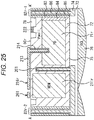
- Fig. 3 is a vertical sectional view of a pixel 50a according to the first embodiment of the pixel 50 to which the present technology is applied
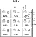
- Fig. 4 is a plan view of the front surface side of the pixel 50a. Note that Fig. 3 corresponds to a position along a line X-X' in Fig. 4 .
- the pixel 50 will be described as a back-illuminated type as an example. However, the present technology can also be applied to a front-illuminated type.
- the pixel 50 shown in Fig. 3 has a photodiode (PD) 71 which is a photoelectric conversion element of each pixel formed inside the Si substrate 70.
- PD photodiode
- a P-type region 72 is formed on the light entrance side (in the figure, lower side that is the back surface side) of the PD 71, and a planarized film 73 is formed further below the P-type region 72.
- the boundary between the P-type region 72 and the planarized film 73 is defined as a backside Si interface 75.
- a light-shielding film 74 is formed in the planarized film 73.
- the light-shielding film 74 is provided to prevent light from leaking into an adjacent pixel, and is formed between adjacent PDs 71.
- the light-shielding film 74 includes, for example, a metal material such as tungsten (W).
- An on-chip lens (OCL) 76 for converging incident light to the PD 71 is formed on the planarized film 73 and on the back surface side of the Si substrate 70.
- An inorganic material can be used for the OCL 76.
- SiN, SiO, or SiOxNy (0 ⁇ x ⁇ 1, 0 ⁇ y ⁇ 1) can be used.
- a cover glass or a transparent plate such as a resin plate may be bonded on the OCL 76.
- a color filter layer may be formed between the OCL 76 and the planarized film 73.
- a plurality of color filters may be provided for each pixel, and the colors of the color filters may be arranged, for example, in a Bayer arrangement.
- An active region (Pwell) 77 is formed on the side (in the figure, upper side that is the front surface side) reverse to the light entrance side of the PD 71.
- a device isolation region hereinafter, referred to as shallow trench isolation (STI)
- STI shallow trench isolation
- a wiring layer 79 is formed on the front surface side (upper side in the figure) of the Si substrate 70 and on the active region 77, and a plurality of transistors is formed in the wiring layer 79.
- Fig. 3 shows an example in which a transfer transistor 80 is formed.
- the transfer transistor (gate) 80 is a vertical transistor. That is, in the transfer transistor (gate) 80, a vertical transistor trench 81 is opened, and a transfer gate (TG) 80 for reading electric charge from the PD 71 is formed therein.
- pixel transistors such as an amplifier (AMP) transistor, a selection (SEL) transistor, and a reset (RST) transistor are formed on the front surface side of the Si substrate 70.
- AMP amplifier
- SEL selection
- RST reset
- a trench is formed between the pixels 50a.
- This trench is referred to as deep trench isolation (DTI) 82.
- the DTI 82 is formed between the adjacent pixels 50a, and penetrates the Si substrate 70 in the depth direction (in the figure, vertical direction, that is, a direction from the front surface to the back surface). Further, the DTI 82 also functions as a light-shielding wall between pixels so that unnecessary light does not leak to the adjacent pixels 50a.
- a P-type solid-phase diffusion layer 83 and an N-type solid-phase diffusion layer 84 are formed between the PD 71 and the DTI 82 in order from the DTI 82 toward the PD 71.
- the P-type solid-phase diffusion layer 83 is formed along the DTI 82 so as to be in contact with the backside Si interface 75 of the Si substrate 70.
- the N-type solid-phase diffusion layer 84 is formed along the DTI 82 so as to be in contact with the P-type region 72 of the Si substrate 70.
- the solid-phase diffusion layer refers to a layer in which a P-type layer and an N-type layer generated by impurity doping are formed in accordance with a method to be described later.
- the method is not limited to a solid-phase diffusion method, and a P-type layer and an N-type layer generated by another method, such as ion implantation, may be provided between the DTI 82 and the PD 71.
- the PD 71 in the embodiment includes an N-type region. The photoelectric conversion is performed in a partial area or entire area of the N-type region.
- the P-type solid-phase diffusion layer 83 is formed so as to be in contact with the backside Si interface 75, while the N-type solid-phase diffusion layer 84 does not contact the backside Si interface 75. Therefore, there is a gap between the N-type solid-phase diffusion layer 84 and the backside Si interface 75.
- the PN junction region between the P-type solid-phase diffusion layer 83 and the N-type solid-phase diffusion layer 84 forms a strong electric field region, and retains electric charge generated in the PD 71.
- the P-type solid-phase diffusion layer 83 and the N-type solid-phase diffusion layer 84 formed along the DTI 82 form a strong electric field region, and can retain electric charge generated in the PD 71.
- the N-type solid-phase diffusion layer 84 is formed along the DTI 82 so as to be in contact with the backside Si interface 75 of the Si substrate 70, pinning of electric charge weakens in the portion where the N-type solid-phase diffusion layer 84 is in contact with the backside Si interface 75 of the Si substrate 70 on the light entrance surface side, resulting in that the generated electric charge flows into the PD 71.
- dark characteristics may deteriorate. For example, a white spot may appear, or a dark current may occur.
- the N-type solid-phase diffusion layer 84 does not contact the backside Si interface 75 of the Si substrate 70, and is formed along the DTI 82 so as to be in contact with the P-type region 72 of the Si substrate 70.
- a sidewall film 85 including SiO2 is formed on the inner wall of the DTI 82, and a filler 86 including polysilicon is embedded inside the sidewall film 85.
- the pixel 50a according to the first embodiment has a configuration in which the P-type region 72 is provided on the back surface side, and the PD 71 and the N-type solid-phase diffusion layer 84 do not exist near the backside Si interface 75. As a result, weakening of pinning near the backside Si interface 75 does not occur. Therefore, deterioration in dark characteristics due to the electric charge flowing into the PD 71 can be prevented.
- SiN may be used for the sidewall film 85 instead of SiO2.
- doping polysilicon may be used for the filler 86 instead of polysilicon.
- application of a negative bias to the resultant filler makes it possible to strengthen pinning on the sidewall of the DTI 82, and thus, the dark characteristics can be further improved.
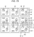
- Fig. 4 is a plan view of nine pixels 50a in 3 x 3 array in the pixel array section 41 ( Fig. 2 ) when viewed from the front surface side (upper side in Fig. 3 ), and Fig. 5 is a circuit diagram for describing a connection relationship between the transistors shown in Fig. 4 .
- one rectangle represents one pixel 50a.
- the DTI 82 is formed so as to surround the pixels 50a (the PDs 71 included in the pixels 50a). Further, a transfer transistor (gate) 80, a floating diffusion (FD) 91, a reset transistor 92, an amplifier transistor 93, and a selection transistor 94 are formed on the front surface of the pixel 50a.
- the PD 71 generates and accumulates electric charges (signal charges) corresponding to an amount of received light.
- the PD 71 has an anode terminal grounded and a cathode terminal connected to the FD 91 via the transfer transistor 80.
- the transfer transistor 80 When turned on by a transfer signal TR, the transfer transistor 80 reads the electric charge generated in the PD 71 and transfers the generated electric charge to the FD 91.
- the FD 91 retains the electric charge read from the PD 71.
- the reset transistor 92 resets the potential of the FD 91 by discharging electric charges accumulated in the FD 91 to a drain (constant voltage source Vdd), when turned on by a reset signal RST.
- the amplifier transistor 93 outputs a pixel signal according to the potential of the FD 91. That is, the amplifier transistor 93 constitutes a source follower circuit with a load MOS (not shown) as a constant current source connected via a vertical signal line 33, and a pixel signal indicating a level according to the electric charge accumulated in the FD 91 is output to the column processor 43 ( Fig. 2 ) from the amplifier transistor 93 via the selection transistor 94 and the vertical signal line 47.
- a load MOS not shown
- the selection transistor 94 is turned on when the pixel 31 is selected by a selection signal SEL, and outputs the pixel signal of the pixel 31 to the column processor 43 via the vertical signal line 33.
- the signal lines to which the transfer signal TR, the selection signal SEL, and the reset signal RST are transmitted correspond to the pixel drive lines 46 in Fig. 2 .
- the pixel 50a can be configured as described above, but is not limited to having the above configuration.
- the pixel 50a may have another configuration.
- Fig. 6 is a diagram for describing a manufacturing method of the DTI 82 and a periphery thereof.
- an SiO2 film containing phosphorus (P), which is an N-type impurity, is formed on the inner side of the opened groove, and then a heat treatment is performed to dope a portion from the SiO2 film into the Si substrate 70 with phosphorus (P) (hereinafter referred to as solid-phase diffusion).
- P phosphorus
- boron (B) is diffused from the SiO2 film toward the Si substrate 70 by solid-phase diffusion, whereby the P-type solid-phase diffusion layer 83 self-aligned to the shape of the extended groove is formed.
- a sidewall film 85 including SiO2 is formed on the inner wall of the opened groove and filled with polysilicon.
- the DTI 82 is formed.
- pixel transistors and wires are formed.
- the Si substrate 70 is thinned from the back surface side.
- the bottom of the DTI 82 including the P-type solid-phase diffusion layer 83 is simultaneously thinned. The thinning process is performed to a depth not reaching the N-type solid-phase diffusion layer 84.
- the strong electric field region constituted by the N-type solid-phase diffusion layer 84 not in contact with the backside Si interface 75 and the P-type solid-phase diffusion layer 83 in contact with the backside Si interface 75 can be formed adjacent to the PD 71.
- Fig. 7 is a vertical sectional view of a pixel 50b according to a second embodiment to which the present technology is applied.
- the second embodiment is different from the first embodiment in that the DTI 82 is formed in the STI 78, and is similar to the first embodiment in the other configurations. Therefore, the portions similar to those in the first embodiment are denoted by the same reference signs, and the description thereof will be omitted as appropriate.
- the same portions as those of the pixel 50b in the first embodiment are denoted by the same reference signs, and the description thereof will be omitted as appropriate.
- an STI 78b formed in the active region 77 is formed up to the portion where a DTI 82b is formed (up to the end of the pixel 50b). Then, the DTI 82b is formed under the STI 78b.
- the STI 78b is formed at the portion where the DTI 82b is formed, and the STI 78b and the DTI 82b are formed at positions where the STI 78b and the DTI 82b are in contact with each other.
- the STI 78b and the DTI 82b are formed at different positions (for example, the pixel 50a ( Fig. 3 ) in the first embodiment).
- the pixel 50b according to the second embodiment can also provide an effect similar to that of the pixel 50a according to the first embodiment, that is, an effect of preventing deterioration in dark characteristics.
- Fig. 8 is a vertical sectional view of a pixel 50c according to a third embodiment to which the present technology is applied.
- the third embodiment is different from the pixels 50a and 50b in the first and second embodiments in that a film 101 having a negative fixed charge is formed on the sidewall of a DTI 82c, and the inside of the film 101 is filled with SiO2 as a filler 86c.
- the pixel 50a in the first embodiment has a configuration in which the sidewall film 85 including SiO2 is formed on the sidewall of the DTI 82 and filled with polysilicon, whereas in the pixel 50c in the third embodiment, the film 101 having a negative fixed charge is formed on the sidewall of the DTI 82c, and the inside of the film 101 is filled with SiO2.
- the film 101 having a negative fixed charge formed on the sidewall of the DTI 82c can be, for example, a hafnium oxide (HfO2) film, an aluminum oxide (Al2O3) film, a zirconium oxide (ZrO2) film, a tantalum oxide (Ta2O5) film, or a titanium oxide (TiO2) film.
- HfO2 hafnium oxide
- Al2O3 aluminum oxide
- ZrO2 zirconium oxide
- Ta2O5 tantalum oxide
- TiO2 titanium oxide
- Examples of the film formation method include a chemical vapor deposition method, a sputtering method, an atomic layer deposition method, and the like. If the atomic layer deposition method is used, an SiO2 layer that reduces the interface state during film formation is simultaneously formed with a thickness of about 1 nm, and thus, preferable.
- examples of the material other than the above materials include lanthanum oxide (La2O3), praseodymium oxide (Pr2O3), cerium oxide (CeO2), neodymium oxide (Nd2O3), promethium oxide (Pm2O3), samarium oxide (Sm2O3), europium oxide (Eu2O3), gadolinium oxide (Gd2O3), terbium oxide (Tb2O3), dysprosium oxide (Dy2O3), holmium oxide (Ho2O3), erbium oxide (Er2O3), thulium oxide (Tm2O3), ytterbium oxide (Yb2O3), lutetium oxide (Lu2O3), and yttrium oxide (Y2O3).
- La2O3 lanthanum oxide
- Pr2O3 praseodymium oxide
- CeO2O3 cerium oxide
- Nd2O3 neodymium oxide
- the film 101 having a negative fixed charge can be formed using a hafnium nitride film, an aluminum nitride film, a hafnium oxynitride film, or an aluminum oxynitride film.
- the film 101 having a negative fixed charge may be added with silicon (Si) or nitrogen (N), as long as the insulating property is not impaired.
- the concentration of the additive is appropriately determined as long as the insulating property of the film is not impaired.
- the additive such as silicon or nitrogen is added to the surface of the film 101 having a negative fixed charge, that is, the surface reverse to the PD71.
- the addition of silicon (Si) and nitrogen (N) makes it possible to increase the heat resistance of the film and the ability to prevent ion implantation during the process.
- the pixel 50c can more reliably prevent deterioration in dark characteristics.
- the DTI 82 in the third embodiment such a process as described below may be performed. Specifically, in the state shown in D of Fig. 6 , the back surface is polished until the polysilicon added as the filler 86 is exposed. Then, the filler 86 (polysilicon) and the sidewall film 85 (SiO2) inside the groove are removed by photoresist and wet etching, and the film 101 is formed. Thereafter, the groove is filled with SiO2.
- the inside of the groove may be filled with a metal material such as tungsten (W) as a filler instead of SiO2.
- a metal material such as tungsten (W) as a filler instead of SiO2.
- Fig. 9 is a vertical sectional view of a pixel 50d according to a fourth embodiment to which the present technology is applied.
- the fourth embodiment is different from the pixel 50a in the first embodiment in that an N-type solid-phase diffusion layer 84d formed along the DTI 82 has a concentration gradient in the depth direction of the Si substrate 70.
- the other configurations are similar to those of the pixel 50a in the first embodiment.
- the N-type impurity concentration of the N-type solid-phase diffusion layer 84 of the pixel 50a in the first embodiment is constant regardless of the depth direction, whereas the N-type impurity concentration of the N-type solid-phase diffusion layer 84d of the pixel 50d in the fourth embodiment varies in the depth direction.
- an N-type solid-phase diffusion layer 84d-1 near the front surface of the N-type solid-phase diffusion layer 84d of the pixel 50d has a high N-type impurity concentration
- an N-type solid-phase diffusion layer 84d-2 near the back surface has a low N-type impurity concentration.
- the pixel 50d according to the fourth embodiment can provide an effect similar to that of the pixel 50a according to the first embodiment.
- the pixel 50d can also provide another effect of making it possible to easily read electric charge due to the potential on the back surface side being shallow by the concentration gradient provided in the N-type solid-phase diffusion layer 84d.
- a concentration gradient can be provided in the N-type solid-phase diffusion layer 84d in the manner described below, for example. Specifically, when a groove for the DTI 82 is opened, etching damage is caused on the sidewall of the groove, and the concentration gradient can be provided by utilizing a difference in a doping amount by solid-phase diffusion due to an amount of damage.
- the concentration of P-type impurities in the P-type solid-phase diffusion layer 83d near the front surface may be reduced, and the concentration of P-type impurities in the P-type solid-phase diffusion layer 83d near the back surface may be increased.
- an effect similar to the effect obtained when the concentration gradient is provided in the N-type solid-phase diffusion layer 84d can also be obtained.
- both the N-type solid-phase diffusion layer 84d and the P-type solid-phase diffusion layer 83d may have a concentration gradient.
- Fig. 10 is a vertical sectional view of a pixel 50e according to a fifth embodiment to which the present technology is applied.
- the pixel 50e according to the fifth embodiment is different from the first embodiment in that a sidewall film 85e including SiO2 and formed on the inner wall of a DTI 82e is formed thicker than the sidewall film 85 of the pixel 50e according to the first embodiment.
- the other configurations are similar to those of the first embodiment.
- SiO2 has a lower refractive index of light than Si. Therefore, light entering the Si substrate 70 is reflected according to Snell's law, so that transmission of light to the adjacent pixel 50 is prevented. However, if the sidewall film 85 is thin, Snell's law is not completely established, and transmitted light may be increased.
- the sidewall film 85e of the pixel 50e in the fifth embodiment is formed to be thick. Therefore, deviation from Snell's law can be reduced, and the reflection of incident light on the sidewall film 85e increases. As a result, transmission of incident light to the adjacent pixel 50e can be reduced. Accordingly, the pixel 50e according to the fifth embodiment can provide an effect similar to the effect of the pixel 50a according to the first embodiment, and can further provide an effect of preventing color mixing to the adjacent pixel 50e due to the obliquely entering light.
- Fig. 11 is a vertical sectional view of a pixel 50f according to a sixth embodiment to which the present technology is applied.
- the pixel 50f according to the sixth embodiment is different from the pixel 50a in the first embodiment in that a region 111 between the PD 71 and the backside Si interface 75 is doped with a P-type impurity, by which a concentration gradient is provided such that the concentration of the P-type impurity is higher on the back surface side than on the front surface side in the Si substrate 70.
- the other configurations are similar to those of the pixel 50a in the first embodiment.
- the Si substrate 70 has no concentration gradient, and the P-type region 72 is formed between the PD 71 and the backside Si interface 75.
- the Si substrate 70 has a concentration gradient. The concentration gradient is such that the concentration of the P-type impurity is higher on the back surface side (P-type region 111 side) than on the front surface side.
- the pixel 50f according to the sixth embodiment having such a concentration gradient can provide an effect similar to that of the pixel 50a according to the first embodiment, and can also provide a further effect of making it easier to read electric charge as compared with the pixel 50a in the first embodiment.
- Fig. 12 is a vertical sectional view of a pixel 50g according to a seventh embodiment to which the present technology is applied.
- the pixel 50g according to the seventh embodiment is different from the pixel 50a according to the first embodiment in that the pixel 50g has a thicker Si substrate 70 than the pixel 50a, and with an increase in the thickness of the Si substrate 70, the DTI 82 or the like is formed deeper.
- the pixel 50g in the seventh embodiment has a thick Si substrate 70g. With an increase in the thickness of the Si substrate 70g, the area (volume) of the PD 71g increases, and a DTI 82g is deeper. Further, since the DTI 82g is formed deeper, a P-type solid-phase diffusion layer 83g and an N-type solid-phase diffusion layer 84g are also formed deeper (wider).
- the pixel 50g according to the seventh embodiment can provide an effect similar to that of the pixel 50g according to the first embodiment, and can further provide an effect of increasing the saturation charge amount Qs as compared with the pixel 50a according to the first embodiment.
- Fig. 13 is a vertical sectional view of a pixel 50h according to an eighth embodiment to which the present technology is applied.
- the length of the Si substrate 70g in the depth direction is increased as in the pixel 50g according to the seventh embodiment shown in Fig. 12 .
- a P-type region 121-1, an N-type region 122, and a P-type region 121-2 are formed in the PD 71 on the back surface side by ion implantation.
- a strong electric field is generated at the PN junction formed by the P-type region 121-1, the N-type region 122, and the P-type region 121-2, whereby electric charge can be retained.
- the pixel 50h according to the eighth embodiment can provide an effect similar to that of the pixel 50g according to the seventh embodiment, and can further provide an effect of increasing the saturation charge amount Qs.
- Fig. 14 is a vertical sectional view of a pixel 50i according to a ninth embodiment to which the present technology is applied.
- the pixel 50i according to the ninth embodiment is different from the pixel 50a according to the first embodiment in that a MOS capacitor 131 and a pixel transistor (not shown) are formed on the front surface side of the Si substrate 70.
- the other configurations are similar to those of the pixel 50a in the first embodiment.
- the pixel 50i has a configuration in which the MOS capacitor 131 is added as a capacitance to be added to the FD 91 (not shown in Fig. 11 ).
- the pixel 50i according to the ninth embodiment can provide an effect similar to that of the pixel 50a according to the first embodiment. Further, the pixel 50i can reduce the conversion efficiency of the PD 71 due to the addition of the MOS capacitor 131 to the FD 91, and can make full use of the increased saturation charge amount Qs.
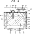
- Fig. 15 is a vertical sectional view of a pixel 50j according to a tenth embodiment to which the present technology is applied.
- the pixel 50j according to the tenth embodiment is different from the pixel 50a according to the first embodiment in that two contacts 152 are formed in a well contact section 151 formed in an active region 77, and the contacts 152 are connected to a Cu wire 153.
- the other configurations are similar to those of the pixel 50a according to the first embodiment.
- the well contact section 151 may be provided. Note that, although Fig. 15 shows an example in which two contacts 152 are formed, two or more contacts 152 may be formed in the well contact section 151.
- the pixel 50j according to the tenth embodiment can provide an effect similar to that of the pixel 50a according to the first embodiment, and can further provide an effect of enhancing critical yield defect.
- Fig. 16 shows a vertical sectional view and a plan view of a pixel 50k according to an eleventh embodiment to which the present technology is applied.
- the pixel 50k according to the eleventh embodiment is different from the pixel 50a according to the first embodiment in that a transfer transistor (gate) 80k is formed by opening a vertical transistor trench 81k in the center of the pixel 50k.
- the other configurations are similar to those of the pixel 50a in the first embodiment.
- the transfer transistor (gate) 80k is positioned equidistant from the outer periphery of the PD 71. Therefore, the pixel 50k according to the eleventh embodiment can provide an effect similar to that of the pixel 50a according to the first embodiment, and further, can improve transfer of electric charge because the transfer transistor (gate) is positioned equidistant from the outer periphery of the PD 71.
- Fig. 17 shows a vertical sectional view and a plan view of a pixel 50m according to a twelfth embodiment to which the present technology is applied.
- the pixel 50m according to the twelfth embodiment is different from the pixel 50a according to the first embodiment in that a transfer transistor 80m includes two vertical transistor trenches 81-1 and 81-2.
- the other configurations are similar to those of the pixel 50a in the first embodiment.
- the pixel 50a ( Fig. 3 ) according to the first embodiment has a configuration in which the transfer transistor 80 includes one vertical transistor trench 81, whereas the pixel 50m according to the twelfth embodiment has a configuration in which the transfer transistor 80m includes two vertical transistor trenches 81-1 and 81-2.
- the followability of the potential in the region between the two vertical transistor trenches 81-1 and 81-2 upon changing the potential of the transfer transistor 80k is improved. Therefore, the degree of modulation can be increased. As a result, the charge transfer efficiency can be improved.
- the transfer transistor 80k includes, as one example, two vertical transistor trenches 81-1 and 81-2 in the above description, two or more vertical transistor trenches 81 may be provided in each pixel region.
- the two vertical transistor trenches 81-1 and 81-2 are formed to have the same size (length and thickness) has been described. However, in a case where multiple vertical transistor trenches 81 are formed, they may have different sizes. For example, one of the two vertical transistor trenches 81-1 and 81-2 may be longer than the other, or thicker than the other.
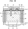
- Fig. 18 is a vertical sectional view of a pixel 50n according to a thirteenth embodiment to which the present technology is applied.
- the pixel 50n according to the thirteenth embodiment is different from the pixel 50a according to the first embodiment in the configuration of the light-shielding film 74, and the other configurations are similar to those of the pixel 50a.
- a light-shielding film 74n-1 and a light-shielding film 74n-2 are formed above and below a DTI 82n, respectively.
- the pixel 50a according to the first embodiment ( Fig. 3 ) has the light-shielding film 74 that covers the back surface side of the DTI 82 (lower side in the figure) on the back surface side thereof, whereas in the pixel 50n ( Fig. 18 ), the DTI 82n is filled with a metal material (for example, tungsten) same as the material of the light-shielding film 74, and the front surface side (upper side in the figure) of the Si substrate 70 is also covered with the metal material.
- a metal material for example, tungsten
- each pixel region is surrounded by the metal material except for the back surface (light entrance surface). It is to be noted, however, that in the configuration in which the pixel 50n is enclosed by the metal material except for the back surface of the pixel 50n, an opening is formed as appropriate at necessary portions. For example, a portion of the light-shielding film 74n-2 where the transfer transistor 80n is located is opened, and a terminal for connection to the outside is formed therein.
- a metal material other than tungsten (W) may be used for the light-shielding film 74 and the like.
- the pixel 50n in the thirteenth embodiment it is possible to prevent the incident light from leaking to the adjacent pixel 50n, so that color mixing can be suppressed.
- the pixel 50n according to the thirteenth embodiment can provide an effect similar to that of the pixel 50a according to the first embodiment, and can further provide an effect of enhancing the sensitivity of the PD 71.
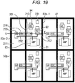
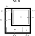
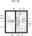
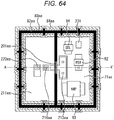
- Fig. 19 is a horizontal plan view of a pixel 50p according to a fourteenth embodiment to which the present technology is applied
- Fig. 20 is a vertical sectional view of the pixel 50p cut along a line A-A' in the pixel 50p shown in Fig. 19 .
- the pixel 50p according to the fourteenth embodiment includes the abovementioned pixel 50 (the pixel 50a herein, for example) and a charge retaining region (corresponding to a memory 211 described below). Due to the charge retaining region being provided, a global shutter can be implemented.
- the pixels 50a to 50p in the first to fourteenth embodiments are back-illuminated sensors.
- a CMOS image sensor is of a rolling shutter type that sequentially reads each pixel, so that image distortion may occur due to a difference in exposure timing.
- a global shutter method for simultaneously reading all pixels by providing a charge retaining section in a pixel has been proposed.
- the read pixels can be sequentially read. Therefore, an exposure timing can be set to be the same in each pixel, and image distortion can be suppressed.
- a PD 71p photoelectric conversion section
- a memory 211 charge retaining section
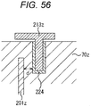
- a part of the substrate between the PD 71p and the memory 211 is drilled, and a light shielding material is embedded in the drilled part.
- the drilled part and the material embedded in the drilled part are shown as a DTI 201.
- the pixel 50p has the PD 71p and the memory 211 formed in a Si substrate 70p.
- the memory 211 is a region having a high N-type impurity concentration like the PD 71p.
- the memory 211 is provided as a charge retaining section that temporarily retains electric charge photoelectrically converted by the PD 71p.
- the pixel 50p is surrounded by a DTI 82p formed so as to penetrate the Si substrate 70p in the depth direction as in the other embodiments, for example, the pixel 50a shown in Fig. 3 .
- a DTI 82p-1 is formed on the right side and a DTI 82p-2 is formed on the left side.
- the DTI 82p is formed to surround the pixel 50a (region including the PD 71p and the memory 211) as shown in the plan view of Fig. 19 .
- a P-type solid-phase diffusion layer 83 and an N-type solid-phase diffusion layer 84 are formed as in the other embodiments. Due to the P-type solid-phase diffusion layer 83 and the N-type solid phase diffusion layer 84, a strong electric field region is formed. Therefore, an effect of preventing deterioration in dark characteristic can be obtained as in the embodiments described above.
- the DTI 201 is provided between the PD 71p and the memory 211 so as not to penetrate the Si substrate 70p in the depth direction. Unlike the DTI 82p surrounding the pixel 50p, the DTI 201 does not penetrate the Si substrate 70p.
- the DTI 201 formed between the PD 71p and the memory 211 is a trench that is drilled with the Pwell region 77 remaining above the DTI 201 (upper part in the figure).
- a read gate 213 is formed on the DTI 201 which is formed in a non-penetrating manner.
- the read gate 213 includes a vertical transistor trench 214, and the vertical transistor trench 214 reaches the inside of the PD 71p. That is, the read gate 213 for reading electric charge from the PD 71p extends in the vertical direction and in the horizontal direction with respect to the PD 71p, and the read gate 213 (vertical transistor trench 214) extending in the vertical direction is formed so as to be in contact with the PD 71p.
- the vertical transistor trench 214 may be formed to be just in contact with the PD 71p or may not be in contact with the PD 71p (with a little distance therebetween). This similarly applies to other vertical transistor trenches.
- a write gate 216 is formed in a region adjacent to the read gate 213.
- the write gate 216 is provided with a vertical transistor trench 217, and the vertical transistor trench 217 reaches (contacts) the inside of the memory 211.
- the DTI 201 is configured not to penetrate the Si substrate 70p in order to provide a region where the read gate 213 and the write gate 216 are formed for enabling such processing.
- a read gate 220 is formed in a region adjacent to the write gate 216.
- the read gate 220 includes a vertical transistor trench 219, and the vertical transistor trench 219 reaches (contacts) the inside of the memory 211.
- the electric charges written (stored) in the memory 211 are read by the read gate 220 and transferred to an amplifier transistor 93 ( Fig. 19 ).
- the read gate 220 and the amplifier transistor 93 are connected by means of an FD wire 232. Further, the amplifier transistor 93 is connected to an N+ diffusion layer 222.
- the N+ diffusion layer 222 is a region provided for suppressing blooming, and has a high N-type impurity concentration. Referring to Fig. 20 , the N+ diffusion layer 222 is formed on the upper right of the PD 71p. In the region on the upper right of the PD 71p, an STI 78 is formed. That is, the region is located on the reverse side to the side where the memory 211 is located.
- the N+ diffusion layer 222 is formed at a position distant from the accumulation region (memory 211) as one example. However, the N+ diffusion layer 222 may be formed near the accumulation region. Further, the N+ diffusion layer 222 is biased to a voltage VDD.
- the DTI 201 between the PD 71p and the memory 211 Due to the formation of the DTI 201 between the PD 71p and the memory 211, it is possible to prevent electric charge from flowing from the PD 71p to the memory 211. However, when the PD 71p is saturated, there is a possibility that electric charge may flow out of the PD 71p to the memory 211 because of the presence of the Pwell region 77 above the DTI 201.
- the N+ diffusion layer 222 is formed so that, when the PD 71p is saturated, electric charge does not flow into the memory 211 from the PD 71p.
- the PD 71p and the memory 211 of the pixel 50p are embedded without using the surface of the Si substrate 70p. Since the PD 71p and the memory 211 are embedded, blooming can be further suppressed.
- the vertical direction in Fig. 20 is defined as a height direction
- the height of the PD 71p is defined as a height H1
- the height of the memory 211 is defined as a height H2
- the height of the DTI 201 is defined as a height H3.
- the pixel 50p has the embedded PD 71p and the memory 211. Therefore, electric charge is read from the PD 71p by the read gate 213 including the vertical transistor trench 214. Further, the read gate 213 is configured to transfer electric charge to the memory 211 over the DTI 201.
- the N+ diffusion layer 222 is formed so that electric charge from the PD 71p does not flow into the memory 211 when the PD 71p is saturated.
- the PD 71p Since the PD 71p is embedded and surrounded by the DTI 82p, electric charge blooms only to the upper side (upper side in Fig. 20 , that is, reverse side to the entrance surface). Further, the N+ diffusion layer 222 biased to the voltage VDD is formed in the direction in which the blooming may occur. Therefore, electric charge overflowing from the PD 71p flows into the N+ diffusion layer 222, and thus, blooming does not occur.
- the N+ diffusion layer 222 is connected to the reset transistor 92, so that electric charge flowing into the N+ diffusion layer 222 can be discharged by turning on the reset transistor 92 during a standby period.
- an effect similar to the effect of the pixel 50a in the first embodiment can be obtained, and further, an effect of suppressing blooming can be obtained.
- Fig. 19 is a plan view of the pixel 50p as viewed from the wiring layer side (the side reverse to the light entrance surface).
- Fig. 19 shows four pixels in 2 x 2 array in the pixel array section 41 ( Fig. 2 ). Focusing on one pixel 50p of the four pixels, in Fig. 19 , the left side of the pixel 50p is an area where the memory 211 is provided, and the right side is an area where the PD 71p is provided.
- the reset transistor 92, the amplifier transistor 93, the selection transistor 94, and the well contact section 231 are formed on the PD 71p. Further, the read gate 213 is formed so as to extend over the PD 71p and the memory 211 and on the DTI 201 formed in a non-penetrating manner.
- the write gate 216 and the read gate 220 are formed on the memory 211. Further, as described above, the read gate 220, the amplifier transistor 93, and the N+ diffusion layer 222 are connected by means of the FD wire 232.
- the FD wire 232 is formed so as to extend over the DTI 201 which is formed in a non-penetrating manner.
- the pixel 50p is surrounded by the DTI 82P (DTI 82p-1 and DTI 82p-2) penetrating the Si substrate 70p. That is, the pixel 50p has a completely separated structure in which the pixels are completely separated from each other.
- the configuration of the back surface side (light entrance side) of the pixel 50p will be described with reference to Fig. 20 .
- the light-shielding film 74 is formed on the back surface side of the pixel 50p.
- the filler 86 formed in the DTI 82p-1 and the light-shielding film 74-1 are connected.
- the light-shielding film 74-1 may include a metal material such as tungsten (W)
- the filler 86 may also include the metal material forming the light-shielding film 74-1
- the filler 86 and the light-shielding film 74-1 may be integrally (continuously) formed.
- the filler 86 and the light-shielding film 74 are continuously formed using the same material.
- the filler 86 in the DTI 82p-2, the light-shielding film 74-2, and the filler in the DTI 201 are also continuously formed using the same material.
- the light-shielding film 74-2 is formed on the light entrance surface side of the memory 211. With this configuration, light does not enter the memory 211 from the light entrance surface side by the light-shielding film 74-2, and stray light from the adjacent pixel 50p (PD 71p) does not enter the memory 211 by the DTI 82p-2 and the DTI 201.
- the pixel 50p is configured such that light does not enter the memory 211.
- the PD 71p is formed with an opening for allowing light to enter.
- the OCL 76 is formed so as to be aligned with the center of the opening (the center in the horizontal direction of the PD 71p).
- the pixel 50p is used as a pixel (ZAF pixel) for detecting a phase difference on an image plane
- a half of the opening in the PD 71p is shielded by the light-shielding film 74, and the height and curvature of the OCL 76 are adjusted so that light is focused on the light-shielding film 74.
- each pixel 50p includes transistors such as the selection transistor 94
- transistors such as the selection transistor 94
- the present technology is applicable to a case where a plurality of pixels 50p shares a predetermined transistor as shown in Fig. 21 .
- a case where the reset transistor 92 and the selection transistor 94 are shared by two pixels 50p arranged in the vertical direction will be described with reference to Fig. 21 .
- Fig. 21 shows four pixels in 2 x 2 array in the pixel array section 41 ( Fig. 2 ). Pixels 50p-1 and 50p-2 arranged in the vertical direction are sharing pixels.
- An amplifier transistor 93-1, a selection transistor 94, a well contact section 231-1, and an N+ diffusion layer 222-1 are formed on a PD 71P-1 of the pixel 50p-1.
- a read gate 213-1 is formed so as to extend over the PD 71P-1 and a memory 211-1 on the pixel 50p-1. Further, a write gate 216-1 and a read gate 220-1 are formed on the memory 211-1 on the pixel 50p-1.
- An amplifier transistor 93-2, a reset transistor 92, a well contact section 231-2, and an N+ diffusion layer 222-2 are formed on a PD 71P-2 of the pixel 50p-2.
- a read gate 213-2 is formed so as to extend over the PD 71P-2 and a memory 211-2 on the pixel 50p-21. Further, a write gate 216-2 and a read gate 220-2 are formed on the memory 211-2 on the pixel 50p-2.
- the amplifier transistor 93-2 of the pixel 50p-2, the N+ diffusion layer 222-2 of the pixel 50p-2, the amplifier transistor 93-1 of the pixel 50p-1, the N+ diffusion layer 222-1 of the pixel 50p-1, the read gate 220-1 of the pixel 50p-1, and the read gate 220-2 of the pixel 50p-2 are connected by means of an FD wire 241.
- the reset transistor 92 and the selection transistor 94 may be shared by two pixels.
- the configuration shown in Fig. 21 is merely an example.
- the amplifier transistors 93 are formed in the pixel 50p-1 and the pixel 50p-2, respectively, as an example.
- the amplifier transistor may be shared. That is, the amplifier transistor 93 may be formed in either of the pixel 50p-1 or the pixel 50p-2.
- a region where the amplifier transistor 93 is disposed can be increased, so that a large amplifier transistor 93 may formed.
- the positions of the reset transistor 92 and the amplifier transistor 93-2 may be switched.
- the pixel size can be reduced, whereby a reduction in size of the imaging device can be achieved.
- step S101 a Si substrate 70p is prepared, and a trench is formed in the Si substrate 70p. Thus, a portion corresponding to the DTI 82p is formed.
- the formed DTI 82p is doped with a P-type impurity by a solid-phase diffusion process, whereby the P-type solid-phase diffusion layer 83 is formed.
- the doping (formation of the P-type solid-phase diffusion layer 83) can be performed by oblique ion implantation or plasma doping instead of solid-phase diffusion. Further, a method may be used in which a P-type impurity layer is formed in advance by performing ion implantation a plurality of times using a resist mask from the surface before the formation of the DTI 82p.
- step S101 such as solid-phase diffusion.
- step S102 after an SiO2 film is formed in the DTI 82p, the DTI 82p is filled with polysilicon 242. Thereafter, the read gate 213 having the vertical transistor trench 214, the write gate 216 having the vertical transistor trench 217, and the read gate 220 having the vertical transistor trench 219 are respectively formed. Then, the Si substrate 70p is polished from the entrance surface side (lower side in the figure), and is thinned until the thickness thereof becomes, for example, about 4 ⁇ m.
- step S103 the DTI 201 (DTI formed in a non-penetrating manner) is formed by etching the Si substrate 70p from the light entrance surface side (the surface reverse to the surface on which the transistors are formed in step S102). After that, the polysilicon 242 with which the DTI 82p is filled is removed. Due to the processes so far, neither the DTI 82p nor the DTI 201 is filled with the filler.
- the DTI 82p and the DTI 201 are filled with a metal material such as tungsten. Further, a film (referred to as a metal film) is formed on the light entrance surface side of the Si substrate 70p using the metal material. The metal film on the light entrance side of the PD 71p in the metal film formed on the light entrance surface side of the Si substrate 70p is removed by a process such as etching, whereby an opening is formed in the PD 71p. After that, the PD 71p, the memory 211, the color filter, the OCL 76, and the like are formed.
- a metal material such as tungsten.
- the DTI 82p that surrounds the pixel 50p and penetrates the Si substrate 70p and the DTI 201 formed in a non-penetrating manner between the PD 71p and the memory 211 are formed at different timings.
- the solid-phase diffusion process is performed at a high temperature, and after such a process at a high temperature (step S101), a metal film serving as the light-shielding film 74 is formed (step S103). Therefore, the metal film is processed without being exposed to a high temperature.
- the side surface of the PD 71p is surrounded by the DTI 82. Therefore, it is possible to prevent electric charge from flowing from the PD 71p to the memory 211, whereby blooming to the memory 211 can be suppressed.
- the N+ diffusion layer 222 is formed above the PD 71p, electric charge overflowing from the PD 71p when the PD 71p is saturated can be received by the N+ diffusion layer 222. Thus, even when the PD 71p is saturated, flow of electric charge from the PD 71p into the memory 211 can be prevented, whereby blooming to the memory 211 can be suppressed.
- the DTI 82p formed in the side surfaces of the PD 71p and the memory 211 has a strong electric field region formed by the p-type solid-phase diffusion layer 83p and the N-type solid-phase diffusion layer 84p, so that the capacity of the PD 71p and the memory 211 can be increased, and the saturation signal amount Qs can be ensured.
- Fig. 23 is a vertical sectional view of a pixel 50q according to a fifteenth embodiment to which the present technology is applied.
- the fifteenth embodiment is different from the fourteenth embodiment in that the DTI 82 is formed in the STI 78, and is similar to the fourteenth embodiment in the other configurations. Therefore, the portions similar to those in the fourteenth embodiment are denoted by the same reference signs, and the description thereof will be omitted as appropriate.
- an STI 78q formed in the active region 77 is formed up to the portion where a DTI 82q is formed (up to the end of the pixel 50q). Then, the DTI 82q is formed under the STI 78q.
- the STI 78q is formed at the portion where the DTI 82q is formed, and the STI 78q and the DTI 82q are formed at positions where the STI 78q and the DTI 82q are in contact with each other.
- the pixel 50q according to the fifteenth embodiment can also provide an effect similar to that of the pixel 50a according to the fourteenth embodiment, that is, an effect of preventing deterioration in dark characteristics and an effect of suppressing blooming.
- Fig. 24 is a horizontal plan view of a pixel 50r according to a sixteenth embodiment to which the present technology is applied
- Fig. 25 is a vertical sectional view of the pixel 50r cut along a line A-A' in the pixel 50r shown in Fig. 24 .
- the PD 71 and the memory 211 are both embedded as an example.
- the present technology is also applicable to a pixel 50 in which one of the PD 71 and the memory 211 is embedded and the other is not embedded.
- a PD 71r is embedded, and a memory 211r is not embedded.
- the memory 211r of the pixel 50r shown in Fig. 25 is formed using the surface of the Si substrate 70 as well. With such a configuration, electric charge can be accumulated near the surface of the Si substrate 70r immediately below the gate, and the capacity of the memory 211r can be increased.
- the height of the PD 71r is defined as a height H1
- the height of the memory 211r is defined as a height H2
- the height of the DTI 201 is defined as a height H3.
- a gate having no vertical transistor trench can be used. That is, as shown in Fig. 25 , a write gate 216r for writing electric charge read from the PD 71r into the memory 211r is constituted by a gate having no vertical transistor trench. Further, the write gate 216r also serves as a memory gate for reading electric charge from the memory 211r.
- a transfer transistor gate 261 is also formed above the memory 211r. In a plan view, as shown in Fig. 25 , the transfer transistor gate 261 is formed on the end side of the region where the memory 211r is formed.
- a reset transistor 92, an amplifier transistor 93, a selection transistor 94, and a well contact section 231 are formed on the PD 71r of the pixel 50r. Further, a read gate 213 is formed on the DTI 201 so as to extend over the PD 71r and the memory 211r. The write gate 216r and the transfer transistor gate 261 are formed on the memory 211r.
- an N+ diffusion layer 222 is formed in the pixel 50r. Therefore, when the PD 71r is saturated, electric charge from the PD 71r does not flow into the memory 211r.
- the pixel 50r according to the sixteenth embodiment can also provide an effect similar to that of the pixel 50a according to the fourteenth embodiment, that is, an effect of preventing deterioration in dark characteristics and an effect of suppressing blooming.
- Fig. 26 is a horizontal plan view of a pixel 50s according to a seventeenth embodiment to which the present technology is applied
- Fig. 27 is a vertical sectional view of the pixel 50s cut along a line A-A' in the pixel 50s shown in Fig. 26 .
- the pixel 50s according to the seventeenth embodiment is different from the pixel 50p according to the fourteenth embodiment in that a transfer gate 271 is added.
- the other configurations are similar to those of the pixel 50p according to the fourteenth embodiment.
- a read gate 213 for reading electric charge from a PD 71s, a transfer gate 271 for transferring the read electric charge to a memory 211s, a write gate 216 for writing the transferred electric charge to the memory 211s, and a read gate 220 for reading the electric charge written to the memory 211s are formed on the front surface side (upper side in the figure) of the pixel 50p.
- the read gate 213, the write gate 216, and the read gate 220 include a vertical transistor trench 214, a vertical transistor trench 217, and a vertical transistor trench 219, respectively.
- a reset transistor 92, a selection transistor 94, and a well contact section 231 are formed on the PD 71s of the pixel 50s. Further, the read gate 213 is formed on a DTI 201s-1 so as to extend over the PD 71s and the memory 211s.
- the transfer gate 271 is formed on a Pwell region 77 existing between the PD 71s and the memory 211s.
- the transfer gate 271 is formed so as to extend over a DTI 201s-2.
- an N+ diffusion layer 272 ( Fig. 26 ) is also formed.
- the write gate 216, the read gate 220, and an amplifier transistor 93 are formed on the memory 211s.
- the DTI 201s-1 and the DTI 201s-2 are formed between the PD 71s and the memory 211s, and the Pwell region 77 is provided between the DTI 201s-1 and the DTI 201s-2.
- the case where two DTIs, the DTI 201s-1 and the DTI 201s-2, are formed is described as an example. However, either the DTI 201s-1 or the DTI 201s-2 may only be formed. Further, the DTI 201s-1 and the DTI 201s-2 may have the same shape, or may have different shapes. For example, one of them may be thicker than the other, or may be higher than the other.
- the arrangement position, shape, size, and the like of the gates of the pixel 50r shown in Figs. 26 and 27 are examples, and other arrangement positions, shapes, sizes, and the like may be employed.
- the transfer gate 271 may be longer than the illustrated transfer gate, and the read gate 213 may be shorter than the illustrated read gate.
- the DTI 201s-1, the DTI 201s-2, and the DTI 82s-2 are continuously formed by being connected via a light-shielding film 74s-2.
- the PD 71p is embedded and surrounded by the DTI 82p and the DTI 201s, whereby electric charge blooms only to the upper side (upper side in Fig. 27 , that is, reverse side to the entrance surface).
- the N+ diffusion layer 222 biased to the voltage VDD is formed in the direction in which the blooming may occur. Therefore, electric charge overflowing from the PD 71s flows into the N+ diffusion layer 222, and thus, blooming does not occur.
- DTI 201s-1 and DTI 201s-2 are formed between the PD 71s and the memory 211s. This makes it possible to enhance the effect of suppressing smear on the memory 211s. Furthermore, due to the formation of two DTIs, the possibility of an occurrence of blooming can be reduced as compared with the case where only one DTI is formed.
- electric charge can be more reliably transferred from the PD 71s to the memory 211 by providing the transfer gate 271.
- the electric charge read from the PD 71s is once held in a region under the transfer gate 271 or both in the region under the transfer gate 271 and in the memory 211s. Then, after the read gate 213 is turned off, all electric charges are moved from the region under the transfer gate 271 to the memory 211s.
- the read gate 213 Since the read gate 213 is turned off when the electric charges are transferred to the memory 211s, it is possible to prevent the electric charges from flowing back to the PD 71s. Therefore, according to the pixel 50s, electric charge can be more reliably transferred from the PD 71s to the memory 211.
- the pixel 50s according to the seventeenth embodiment can also provide an effect similar to that of the pixel 50a according to the fourteenth embodiment, that is, an effect of preventing deterioration in dark characteristics and an effect of suppressing blooming. Further, according to the pixel 50s in the seventeenth embodiment, it is possible to more reliably transfer electric charge from the PD 71s to the memory 211.
- Fig. 28 is a horizontal plan view of a pixel 50t according to an eighteenth embodiment to which the present technology is applied
- Fig. 29 is a vertical sectional view of the pixel 50t cut along a line A-A' in the pixel 50t shown in Fig. 28 .
- the pixel 50t according to the eighteenth embodiment has a configuration obtained by combining the configuration of the pixel 50r according to the sixteenth embodiment and the configuration of the pixel 50s according to the seventeenth embodiment. That is, the pixel 50t in the eighteenth embodiment has a configuration in which a memory 211t is not embedded like the pixel 50r in the sixteenth embodiment, and has a transfer gate 271 like the pixel 50s in the seventeenth embodiment.
- the memory 211t of the pixel 50t is formed using the surface of the Si substrate 70 as well. With such a configuration, electric charge can be accumulated near the surface of the Si substrate 70t immediately below the gate, and the capacity of the memory 211t can be increased.
- the vertical direction in Fig. 29 is defined as a height direction
- the height of a PD 71t is defined as a height H1
- the height of the memory 211t is defined as a height H2
- the height of the DTI 201 is defined as a height H3.
- a gate having no vertical transistor trench can be used. That is, as shown in Fig. 29 , the transfer gate 271 that transfers the electric charge read from the PD 71t to the memory 211t and the memory gate 281 are constituted by gates having no vertical transistor trench.
- the memory gate 281 is a gate that performs writing and reading of electric charge from the memory 211t.
- a reset transistor 92, an amplifier transistor 93, a selection transistor 94, and a well contact section 231 are formed on the PD 71t of the pixel 50t. Further, a read gate 213 is formed on a DTI 201t-1 so as to extend over the PD 71t and the memory 211t.
- a transfer gate 271 is formed on a Pwell region 77 existing between the PD 71t and the memory 211t.
- the transfer gate 271 is formed so as to extend over the DTI 201t-2.
- an N+ diffusion layer 272 is also formed in the Pwell region 77 existing between the PD 71t and the memory 211t.
- a memory gate 281 and a transfer transistor gate 261 are formed on the memory 211t.
- an N+ diffusion layer 222 is formed in the pixel 50t. Therefore, when the PD 71t is saturated, electric charge from the PD 71t does not flow into the memory 211t.
- the pixel 50t according to the eighteenth embodiment can also provide an effect similar to that of the pixel 50a according to the fourteenth embodiment, that is, an effect of preventing deterioration in dark characteristics and an effect of suppressing blooming. Further, according to the pixel 50t in the eighteenth embodiment, electric charge can be more reliably transferred from the PD 71t to the memory 211t.
- Fig. 30 is a horizontal plan view of a pixel 50u according to a nineteenth embodiment to which the present technology is applied
- Fig. 31 is a vertical sectional view of the pixel 50u cut along a line A-A' in the pixel 50u shown in Fig. 30
- Fig. 32 is a vertical sectional view of the pixel 50u cut along a line B-B' in the pixel 50u shown in Fig. 30 .
- the PD 71 is embedded as an example.
- the present technology is also applicable to a pixel 50 in which the PD 71 is not embedded.
- a PD 71u is not embedded, and a memory 211r is embedded.
- the PD 71u of the pixel 50u shown in Fig. 31 is formed using the surface of the Si substrate 70 as well. With such a configuration, an electric field can be ensured, and the saturation signal amount Qs can be increased.
- the height of the PD 71u is defined as a height H1
- the height of the memory 211u is defined as a height H2
- the height of the DTI 201 is defined as a height H3.
- a gate having no vertical transistor trench can be used. That is, as shown in Fig. 31 , a read gate 291 for reading electric charge from the PD 71u is constituted by a gate having no vertical transistor trench.
- a write gate 216 has a vertical transistor trench 217, and a read gate 220 has a vertical transistor trench 219.
- an N+ diffusion layer 293 is formed so that electric charge from the PD 71u does not flow into the memory 211u when the PD 71u is saturated.
- the N+ diffusion layer 293 is formed near an amplifier gate 292 and between the DTI 201 and the amplifier gate 292, as shown in Fig. 32 . In this case, the N+ diffusion layer 293 is formed at the drain of the amplifier transistor 93.
- an N+ diffusion layer 222u is also formed at the drain of the reset transistor 92.
- the N+ diffusion layer 293 and the N+ diffusion layer 222u are biased to voltage VDD.
- a read gate 291 is formed on the DTI 201 so as to extend over the PD 71u and the memory 211u. Further, a reset transistor 92, an amplifier transistor 93, a selection transistor 94, and a well contact section 231 are formed on the memory 211u. Moreover, as described above, the N+ diffusion layer 222u is formed at the drain of the reset transistor 92, and the N+ diffusion layer 293 is formed at the drain of the amplifier transistor 93.
- the pixel 50u can be manufactured by a manufacturing process similar to the manufacturing process (for example, the process described with reference to Fig. 22 ) of the abovementioned pixel 50, for example, pixel 50p ( Fig. 20 ).
- the N+ diffusion layer 293 (N+ diffusion layer 222u) of the pixel 50u is formed at a position as described below.
- the N+ diffusion layer 293 (N+ diffusion layer 222u) and the PD 71u need to be positioned distant from each other to some extent so as to prevent the potential barrier in this portion from being lowered.
- the distance between the N+ diffusion layer 293 (N+ diffusion layer 222u) and the PD 71u is set in consideration of such factors.
- the distance between the N+ diffusion layer 293 (N+ diffusion layer 222u) and the PD 71u can be set to about 0.2 ⁇ m to 1 ⁇ m.
- the pixel 50u according to the nineteenth embodiment can also provide an effect similar to that of the pixel 50a according to the fourteenth embodiment, that is, an effect of preventing deterioration in dark characteristics and an effect of suppressing blooming.
- DTI 82 in the STI 78 by combining the fifteenth embodiment ( Fig. 23 ) and the nineteenth embodiment.
- a gate corresponding to the transfer gate 271 between the read gate 291 ( Fig. 31 ) and the write gate 216 by combining the seventeenth embodiment ( Fig. 27 ) and the nineteenth embodiment.
- Fig. 33 is a horizontal plan view of a pixel 50v according to a twentieth embodiment to which the present technology is applied
- Fig. 34 is a view showing a positional relation between a PD 71v and a memory 211v in the pixel 50v shown in Fig. 33
- Fig. 35 is a vertical sectional view of the pixel 50v cut along a line A-A' in the pixel 50v shown in Fig. 33 .
- the twentieth embodiment can be applied to any of the fourteenth to nineteenth embodiments described above. That is, the twentieth embodiment described below can be applied to a case where both the PD 71 and the memory 211 are embedded and a case where either of the PD 71 or the memory 211 is embedded.
- the basic configuration of the pixel 50v according to the twentieth embodiment is similar to that of the pixel 50t ( Figs. 28 and 29 ) according to the eighteenth embodiment, and therefore, the detailed description thereof will be omitted.
- the pixel 50v according to the twentieth embodiment includes a transfer gate 271v, like the pixel 50t according to the eighteenth embodiment, but the transfer gate 271v of the pixel 50v is longer than the transfer gate 271 of the pixel 50t.
- the transfer gate 271v is formed in a portion except for the portion where the read gate 213 and the memory gate 281 are formed along the side where a DTI 82v-2 is formed. Since the transfer gate 271v is longer as described above, the PD 71v and the memory 211v can be arranged at positions distant from each other. This will be described with reference to Fig. 34 .
- Fig. 34 is a horizontal plan view of the pixel 50v, showing positions of the PD 71v and the memory 211v.
- the PD 71v is formed in a rectangular shape on the upper right side of the pixel 50v in the figure. Referring to Fig. 33 together, the PD 71v is formed in a region where a reset transistor 92, an amplifier transistor 93, a selection transistor 94, and a well contact section 231 are formed.
- the memory 211v is formed in a rectangular shape in a lower part of the pixel 50v in the figure. Referring to Fig. 33 together, the memory 211v is formed immediately below a memory gate 281v.
- the PD 71v is surrounded by a DTI 82v penetrating the Si substrate 70 except for the portion where the DTI 201 is formed.
- the portion surrounded by the DTI 82v has a structure capable of preventing light from leaking from the PD 71v to the memory 211v.
- the DTI 201 does not penetrate the Si substrate 70. There is a possibility that light leaks from the PD 71v to the memory 211v via the portion where the DTI 201 is formed, in other words, the Pwell region 77 where the DTI 201 does not penetrate.
- the distance from the PD 71v to the memory 211v via the DTI 201v and the Pwell region 77 immediately below the transfer gate 271v is long, and the memory 211v is not formed near the DTI 201v. Therefore, light leakage from the PD 71v to the memory 211v can be prevented.
- the pixel 50v according to the twentieth embodiment can suppress a stray light component more than the abovementioned embodiments due to the PD 71v and the memory 211v being positioned distant from each other.
- Fig. 35 which is a vertical sectional view of the pixel 50v will be referred to.
- the memory 211v is not embedded as one example. Therefore, the memory 211v is formed using the surface of the Si substrate 70 as shown in Fig. 35 . With such a configuration, electric charge can be accumulated also near the surface of the Si substrate 70v immediately below the gate, and the capacity of the memory 211v can be increased.
- the transfer gate 271 that transfers the electric charge read from the PD 71v to the memory 211v and the memory gate 281 are constituted by gates having no vertical transistor trench. Since the transfer gate 271v is provided, electric charge read from the PD 71v is once held in a region under the transfer gate 271v or both in the region under the transfer gate 271v and in the memory 211v. Then, after the read gate 213 is turned off, all electric charges are moved from the region under the transfer gate 271v to the memory 211v. Therefore, electric charge can be more reliably transferred from the PD 71v to the memory 211v.
- DTI 201v In the pixel 50v shown in Figs. 33 to 35 , only one DTI 201v is formed as one example. However, two DTIs, a DTI 201v-1 and a DTI 201v-2 corresponding to the DTI 201t-1 and the DTI 201t-2 shown in Figs. 28 and 29 , may be formed, for example.
- the pixel 50v according to the twentieth embodiment also has an N+ diffusion layer 222. Therefore, when the PD 71v is saturated, electric charge from the PD 71v does not flow into the memory 211v.
- the pixel 50v according to the twentieth embodiment can also provide an effect similar to that of the pixel 50a according to the fourteenth embodiment, that is, an effect of preventing deterioration in dark characteristics and an effect of suppressing blooming. Further, according to the pixel 50v in the twentieth embodiment, electric charge can be more reliably transferred from the PD 71v to the memory 211v. Furthermore, according to the pixel 50v in the twentieth embodiment, a stray light component can be further suppressed.
- the transfer gate 271v is formed longer because the PD 71v and the memory 211v are positioned distant from each other.
- the transfer efficiency may be reduced.
- a multi-stage transfer gate as shown in Figs. 36 and 37 may be provided.
- a pixel 50v' shown in Figs. 36 and 37 is referred to as an embodiment 20-2, and components different from those of the pixel 50v according to the embodiment 20-1 are denoted with a dash in order to be distinguished from the components in the pixel 50v.
- Fig. 36 is a horizontal plan view of the pixel 50v' according to the embodiment 20-2 to which the present technology is applied
- Fig. 37 is a vertical sectional view of the pixel 50v' cut along a line A-A' in the pixel 50v' shown in Fig. 36 .
- the pixel 50v' is different from the pixel 50v shown in Fig. 33 in that a transfer gate 271v' has a two-stage structure including a transfer gate 271v'-1 and a transfer gate 271v'-2.
- the other configurations are the same as those of the pixel 50v.
- the transfer gate 271v' may have three or more stages.
- DTI 201v' In the pixel 50v' shown in Figs. 36 and 37 , only one DTI 201v' is formed as one example. However, two or more non-penetrating DTIs can be formed.
- the pixel 50v' according to the embodiment 20-2 also has an N+ diffusion layer 222. Therefore, when the PD 71v is saturated, electric charge from the PD 71v does not flow into the memory 211v.
- the pixel 50v' according to the embodiment 20-2 can also provide an effect of preventing deterioration in dark characteristics and an effect of suppressing blooming. Further, according to the pixel 50v' in the embodiment 20-2, electric charge can be more reliably transferred from the PD 71v to the memory 211v. Furthermore, according to the pixel 50v' in the embodiment 20-2, a stray light component can be further suppressed.
- Fig. 38 is a horizontal plan view of a pixel 50v" according to the embodiment 20-3 to which the present technology is applied
- Fig. 39 is a vertical sectional view of the pixel 50v" cut along a line B-B' in the pixel 50v" shown in Fig. 38
- the sectional view of Fig. 35 is applied as a vertical sectional view of the pixel 50v" cut along a line A-A' of the pixel 50v".
- the basic configuration of the pixel 50v" according to the embodiment 20-3 is similar to that of the pixel 50v according to the embodiment 20-1. Therefore, the similar portions are denoted by the same reference signs, and the description thereof will be omitted.
- the pixel 50v" according to the embodiment 20-3 is different from the pixel 50v according to the embodiment 20-1 in that a drain discharge section 273 is added.
- the other configurations are the same as those of the pixel 50v.
- the drain discharge section 273 is formed in a region between the region where a transfer gate 271v" is formed and a DTI 82v-3. Referring to the sectional view shown in Fig. 39 , the drain discharge section 273 has the same configuration as the N+ diffusion layer 222 ( Fig. 35 ), and is a region having a high N-type impurity concentration. An STI 78" is formed on each side of the drain discharge section 273. Further, the drain discharge section 273 is connected to an N+ layer 274 formed in the Si substrate 70.
- the N+ layer 274 is formed so as not to contact the transfer gate 271v". In other words, the N+ layer 274 is formed so as to avoid the region on the surface side of the Si substrate 70 where the transfer gate 271v" is formed.
- drain discharge section 273 is biased to the voltage VDD. Electric charge accumulated in the N+ layer 274 is discharged from the drain discharge section 273 by applying the voltage VDD to the drain discharge section 273.
- the drain discharge section 273 Due to the formation of the drain discharge section 273 as described above, even if light entering a PD 71v" leaks through the non-penetrating portion of the DTI 201v toward the side where the transfer gate 271v" is formed, the light is photoelectrically converted in the N+ layer 274, and the photoelectrically converted electric charge can be discharged from the drain discharge section 273. Therefore, a stray light component can be suppressed.
- the pixel 50V" shown in Fig. 38 is configured by adding the drain discharge section 273 to the pixel 50v ( Fig. 33 ) according to the embodiment 20-1.
- the drain discharge section 273 may be added to the pixel 50v' ( Fig. 36 ) according to the embodiment 20-2. That is, a configuration in which the drain discharge section 273 is added and the multi-stage transfer gate 271v" is formed may be applied.
- DTI 201v' is formed in the pixel 50v" shown in Fig. 38 as one example, two or more non-penetrating DTIs may be formed.
- the pixel 50v" according to the embodiment 20-3 also has the N+ diffusion layer 222. Therefore, when the PD 71v is saturated, electric charge from the PD 71v does not flow into the memory 211v.
- the pixel 50v" according to the embodiment 20-3 can also provide an effect of preventing deterioration in dark characteristics and an effect of suppressing blooming. Further, according to the pixel 50v" in the embodiment 20-3, electric charge can be more reliably transferred from the PD 71v to the memory 211v. Furthermore, according to the pixel 50v" in the embodiment 20-3, a stray light component can be further suppressed.
- Fig. 40 is a horizontal plan view of a pixel 50w according to a twenty-first embodiment to which the present technology is applied, when viewed from a wiring layer side.
- the sectional view of Fig. 35 is applied as a vertical sectional view of the pixel 50w cut along a line A-A' of the pixel 50w shown in Fig. 40 .
- Fig. 41 is a horizontal plan view of the pixel 50w shown in Fig. 40 , as viewed from the light entrance surface side.
- the twenty-first embodiment can also be applied to any of the fourteenth to nineteenth embodiments described above. That is, the twenty-first embodiment described below can be applied to a case where both the PD 71 and the memory 211 are embedded and a case where either of the PD 71 or the memory 211 is embedded.
- the basic configuration of the pixel 50w according to the twenty-first embodiment is similar to that of the pixel 50v ( Fig. 33 ) according to the twentieth embodiment, and therefore, the detailed description thereof will be omitted.
- the pixel 50w according to the twenty-first embodiment includes a transfer gate 271w, like the pixel 50v according to the twentieth embodiment, but the transfer gate 271w of the pixel 50w is longer than the transfer gate 271v of the pixel 50v. Further, a read gate 213w of the pixel 50w is formed longer than the read gate 213 of the pixel 50v.
- the transfer gate 271w is formed along a side where a DTI 82w-2 is formed, and one end thereof is bent and extends to a memory gate 281w.
- the transfer gate 271w is formed in an L shape.
- the read gate 213w is also formed in an L shape.
- the read gate 213w is formed along a side where a DTI 82w-5 is formed, and one end thereof is bent and extends to the PD 71w.
- a light-shielding film 275 is formed on the light entrance surface side of the pixel 50w.
- the light-shielding film 275 is formed in a region of the pixel 50w except for the region where the PD 71w is formed. In other words, the light-shielding film 275 is formed on a region where the memory 211w and the transfer gate 271w are formed.
- the light-shielding film 275 is formed on the memory 211w so that incident light does not enter the memory 211w.
- the PD 71w is formed in a region on the upper right part of the pixel 50w where the light-shielding film 275 is not formed.
- the memory 211w is formed in a rectangular shape in a lower part of the pixel 50w in the figure.
- the portion except for the PD 71 is also covered with the light-shielding film 275, so that a stray light component does not enter the memory or the like.
- the PD 71w is surrounded by a DTI 82w penetrating the Si substrate 70 except for the portion where a DTI 201w is formed.
- the portion surrounded by the DTI 82w has a structure capable of preventing light from leaking from the PD 71w to the memory 211w.
- the DTI 201w does not penetrate the Si substrate 70. Light entering the PD 71w through the portion where the DTI 201w is formed may leak to a region other than the PD 71w. However, the distance from the PD 71w to the memory 211w via the DTI 201w and the Pwell region 77 immediately below the transfer gate 271w is long, and the memory 211w is not formed near the DTI 201w. Therefore, light leakage from the PD 71w to the memory 211w can be prevented.
- the DTI 201w is formed at a position parallel to the long side of the memory 211w. Since the DTI 201w is formed at such a position, even if light obliquely enters the PD 71w and leaks through a non-penetrating portion of the DTI 201w, such light goes to the DTI 82w-5 side, and is unlikely to reach the memory 211w.
- the pixel 50w according to the twenty-first embodiment can suppress a stray light component due to the PD 71w and the memory 211w being positioned distant from each other.
- DTI 201w In the pixel 50w shown in Fig. 40 , only one DTI 201w is formed as one example. However, two DTIs, a DTI 201w-1 and a DTI 201w-2 corresponding to the DTI 201t-1 and the DTI 201t-2 shown in Figs. 28 and 29 , may be formed, for example.
- the pixel 50w according to the twenty-first embodiment also has an N+ diffusion layer 222. Therefore, when the PD 71w is saturated, electric charge from the PD 71w does not flow into the memory 211w.
- the pixel 50w according to the twenty-first embodiment can also provide an effect similar to that of the pixel 50a according to the fourteenth embodiment, that is, an effect of preventing deterioration in dark characteristics and an effect of suppressing blooming. Further, according to the pixel 50w in the twenty-first embodiment, electric charge can be more reliably transferred from the PD 71w to the memory 211w. Furthermore, according to the pixel 50w in the twenty-first embodiment, a stray light component can be further suppressed.
- the transfer gate 271w is formed longer because the PD 71w and the memory 211w are positioned distant from each other.
- the transfer efficiency may be reduced.
- a multi-stage transfer gate as shown in Fig. 42 may be provided.
- the pixel 50w' shown in Fig. 42 is referred to as an embodiment 21-2, and components different from those of the pixel 50w according to the embodiment 21-1 are denoted with a dash in order to be distinguished from the components in the pixel 50w.
- Fig. 42 is a horizontal plan view of the pixel 50w' according to the embodiment 21-2 to which the present technology is applied.
- the sectional view of Fig. 37 is applied as a vertical sectional view of the pixel 50w' cut along a line A-A' of the pixel 50w' shown in Fig. 42 .
- the pixel 50w' is different from the pixel 50w shown in Fig. 40 in that a transfer gate 271w' has a two-stage structure including a transfer gate 271w'-1 and a transfer gate 271w'-2.
- the other configurations are the same as those of the pixel 50w.
- transfer gate 271w' may have three or more stages.
- DTI 201w' In the pixel 50w' shown in Fig. 42 , only one DTI 201w' is formed as one example. However, two or more non-penetrating DTIs may be formed.
- the pixel 50w' according to the embodiment 21-2 also has an N+ diffusion layer 222. Therefore, when the PD 71w is saturated, electric charge from the PD 71w does not flow into the memory 211w.
- the pixel 50w' according to the embodiment 21-2 can also provide an effect of preventing deterioration in dark characteristics and an effect of suppressing blooming. Further, according to the pixel 50w' in the embodiment 21-2, electric charge can be more reliably transferred from the PD 71w to the memory 211w. Furthermore, according to the pixel 50w' in the embodiment 21-2, a stray light component can be further suppressed.
- Fig. 43 is a horizontal plan view of a pixel 50w" according to the embodiment 21-3 to which the present technology is applied.
- the sectional view of Fig. 35 is applied as a vertical sectional view of the pixel 50w" cut along a line A-A' of the pixel 50w".
- the sectional view of Fig. 39 is applied as a vertical sectional view of the pixel 50w" cut along a line B-B' of the pixel 50w" shown in Fig. 43 .
- the basic configuration of the pixel 50w" according to the embodiment 21-3 is similar to that of the pixel 50w according to the embodiment 21-1. Therefore, the similar portions are denoted by the same reference signs, and the description thereof will be omitted.
- the pixel 50w" according to the embodiment 21-3 is different from the pixel 50w according to the embodiment 21-1 in that a drain discharge section 273w is added.
- the other configurations are the same as those of the pixel 50w.
- the drain discharge section 273w is formed in a region between the region where a transfer gate 271w" is formed and a DTI 82w-3. As in the pixel 50v" according to the embodiment 20-3 described with reference to Fig. 39 , the drain discharge section 273w has the same configuration as the N+ diffusion layer 222 ( Fig. 35 ), and is a region having a high N-type impurity concentration. An STI 78" is formed on each side of the drain discharge section 273. Further, the drain discharge section 273 is connected to an N+ layer 274 formed in the Si substrate 70.
- the N+ layer 274 is formed so as not to contact the transfer gate 271w". In other words, the N+ layer 274 is formed so as to avoid the region on the surface side of the Si substrate 70 where the transfer gate 271w" is formed.
- drain discharge section 273w is biased to the voltage VDD. Electric charge accumulated in the N+ layer 274 is discharged from the drain discharge section 273w by applying the voltage VDD to the drain discharge section 273w.
- the drain discharge section 273w Due to the formation of the drain discharge section 273w as described above, even if light entering a PD 71w" leaks through the non-penetrating portion of the DTI 201w toward the side where the transfer gate 271w" is formed, the light is photoelectrically converted in the N+ layer 274, and the photoelectrically converted electric charge can be discharged from the drain discharge section 273w. Therefore, a stray light component can be suppressed.
- the pixel 50V" shown in Fig. 43 is configured by adding the drain discharge section 273w to the pixel 50w ( Fig. 40 ) according to the embodiment 21-1.
- the drain discharge section 273w may be added to the pixel 50w' ( Fig. 42 ) according to the embodiment 21-2. That is, a configuration in which the drain discharge section 273w is added and the multi-stage transfer gate 271w" is formed may be applied.
- DTI 201w' is formed in the pixel 50w" shown in Fig. 43 as one example, two or more non-penetrating DTIs may be formed.
- the pixel 50w" according to the embodiment 21-3 also has an N+ diffusion layer 222. Therefore, when the PD 71w is saturated, electric charge from the PD 71w does not flow into the memory 211w.
- the pixel 50w" according to the embodiment 21-3 can also provide an effect of preventing deterioration in dark characteristics and an effect of suppressing blooming. Further, according to the pixel 50w" in the embodiment 21-3, electric charge can be more reliably transferred from the PD 71w to the memory 211w. Furthermore, according to the pixel 50w" in the embodiment 21-3, a stray light component can be further suppressed.
- Fig. 44 is a horizontal plan view of a pixel 50x according to a twenty-second embodiment to which the present technology is applied, when viewed from a wiring layer side.
- the sectional view of Fig. 35 is applied as a vertical sectional view of the pixel 50x cut along a line A-A' of the pixel 50x shown in Fig. 44 .
- the twenty-second embodiment can be applied to any of the fourteenth to nineteenth embodiments described above. That is, the twenty-second embodiment described below can be applied to a case where both the PD 71 and the memory 211 are embedded and a case where either of the PD 71 or the memory 211 is embedded.
- the basic configuration of the pixel 50x according to the twenty-second embodiment is similar to that of the pixel 50w ( Fig. 40 ) according to the twenty-first embodiment, and therefore, the detailed description thereof will be omitted.
- the pixel 50x according to the twenty-second embodiment includes a transfer gate 271x, like the pixel 50w according to the twenty-first embodiment, but the transfer gate 271x of the pixel 50x is longer than the transfer gate 271w of the pixel 50w.
- a PD 71w of the pixel 50x in the twenty-second embodiment has a larger light receiving surface than the PD 71w of the pixel 50w in the twenty-first embodiment. Since the PD 71x is formed larger, the transfer gate 271x formed along one side of the PD 71x is also formed longer.
- the PD 71w of the pixel 50x in the twenty-second embodiment has a larger light receiving surface than the PD 71w of the pixel 50w in the twenty-first embodiment. Thus, the PD 71x has higher sensitivity than the PD 71w.
- the transfer gate 271x is formed along the side where a DTI 82x-2 is formed.
- a read gate 213x is formed into an L shape. Specifically, the read gate 213x extends along a side where a DTI 82x-6 is formed, and further, one end thereof is bent and extends to the PD 71x.
- Fig. 45 is a view showing that the pixels 50x are vertically arranged.
- a pixel 50x-1 and a pixel 50x-2 which are pixels 50x are vertically arranged, they are horizontally symmetrical.
- a transfer gate 271x-1 of the pixel 50x-1 is arranged on the left side in the figure
- a transfer gate 271x-2 of the pixel 50x-2 is arranged on the right side in the figure.
- a memory gate 281x-1 (memory 211x-1) of the pixel 50x-1, a transfer gate 261x-1 of the pixel 50x-1, and a read gate 213x-2 of the pixel 50x-2 are linearly arranged between a PD 71x-1 of the pixel 50x-1 and a PD 71x-2 of the pixel 50x-2.
- the PD 71x is surrounded by a DTI 82x penetrating the Si substrate 70 except for the portion where a DTI 201x is formed.
- the portion surrounded by the DTI 82x has a structure capable of preventing light from leaking from the PD 71x to the memory 211x.
- the DTI 201x does not penetrate the Si substrate 70. Light entering the PD 71x through the portion where the DTI 201x is formed may leak to a region other than the PD 71x. However, the distance from the PD 71x to the memory 211x via the DTI 201x and the Pwell region 77 immediately below the transfer gate 271x is long, and the memory 211x is not formed near the DTI 201x. Therefore, light leakage from the PD 71x to the memory 211x can be prevented.
- the DTI 201x is formed at a position parallel to the long side of the memory 211x. Since the DTI 201x is formed at such a position, even if light obliquely enters the PD 71x and leaks through a non-penetrating portion of the DTI 201x, such light goes to the DTI 82x-6 side, and is unlikely to reach the memory 211x.
- the pixel 50x according to the twenty-second embodiment can suppress a stray light component due to the PD 71x and the memory 211x being positioned distant from each other.
- the PD 71x and the memory 211x are more distant from each other, as compared with the configuration of the pixel 50w ( Fig. 40 ) according to the twenty-first embodiment. Therefore, the pixel 50x according to the twenty-second embodiment can suppress a stray light component more than the pixel 50w according to the twenty-first embodiment. Further, the PD 71w of the pixel 50x according to the twenty-second embodiment has a larger light receiving surface than the PD 71w of the pixel 50w according to the twenty-first embodiment. Thus, the pixel 50x according to the twenty-second embodiment can improve sensitivity more than the pixel 50w according to the twenty-first embodiment.
- DTI 201x In the pixel 50x shown in Fig. 44 , only one DTI 201x is formed as one example. However, two DTIs, a DTI 201x-1 and a DTI 201x-2 corresponding to the DTI 201t-1 and the DTI 201t-2 shown in Figs. 28 and 29 , may be formed, for example.
- the pixel 50x according to the twenty-second embodiment also has an N+ diffusion layer 222. Therefore, when the PD 71x is saturated, electric charge from the PD 71x does not flow into the memory 211x.
- the pixel 50x according to the twenty-second embodiment can also provide an effect similar to that of the pixel 50a according to the fourteenth embodiment, that is, an effect of preventing deterioration in dark characteristics and an effect of suppressing blooming. Further, according to the pixel 50x in the twenty-second embodiment, electric charge can be more reliably transferred from the PD 71x to the memory 211x. Furthermore, according to the pixel 50x in the twenty-second embodiment, a stray light component can be further suppressed.
- the transfer gate 271x is formed longer because the PD 71x and the memory 211x are positioned distant from each other. When the transfer gate 271x is longer, the transfer efficiency may be reduced.
- a multi-stage transfer gate as shown in Fig. 46 may be provided.
- a pixel 50x' shown in Fig. 46 is referred to as an embodiment 22-2, and components different from those of the pixel 50x according to the embodiment 22-1 are denoted with a dash in order to be distinguished from the components in the pixel 50x.
- Fig. 46 is a horizontal plan view of the pixel 50x' according to the embodiment 22-2 to which the present technology is applied.
- the sectional view of Fig. 37 is applied as a vertical sectional view of the pixel 50x' cut along a line A-A' of the pixel 50x' shown in Fig. 46 .
- the pixel 50x' is different from the pixel 50x shown in Fig. 44 in that a transfer gate 271x' has a two-stage structure including a transfer gate 271x'-1 and a transfer gate 271x'-2.
- the other configurations are the same as those of the pixel 50x.
- transfer gate 271x' may have three or more stages.
- DTI 201x' In the pixel 50x' shown in Fig. 46 , only one DTI 201x' is formed as one example. However, two or more non-penetrating DTIs may be formed.
- the pixel 50x' according to the embodiment 22-2 also has an N+ diffusion layer 222. Therefore, when the PD 71x is saturated, electric charge from the PD 71x does not flow into the memory 211x.
- the pixel 50x' according to the embodiment 22-2 can also provide an effect of preventing deterioration in dark characteristics and an effect of suppressing blooming. Further, according to the pixel 50x' in the embodiment 22-2, electric charge can be more reliably transferred from the PD 71x to the memory 211x. Furthermore, according to the pixel 50x' in the embodiment 22-2, a stray light component can be further suppressed.
- Fig. 47 is a horizontal plan view of a pixel 50x" according to the embodiment 22-3 to which the present technology is applied.
- the sectional view of Fig. 35 is applied as a vertical sectional view of the pixel 50x" cut along a line A-A' of the pixel 50x".
- the sectional view of Fig. 39 is applied as a vertical sectional view of the pixel 50x" cut along a line B-B' of the pixel 50x" shown in Fig. 47 .
- the basic configuration of the pixel 50x" according to the embodiment 22-3 is similar to that of the pixel 50x according to the embodiment 22-1. Therefore, the similar portions are denoted by the same reference signs, and the description thereof will be omitted.
- the pixel 50x" according to the embodiment 22-3 is different from the pixel 50x according to the embodiment 22-1 in that a drain discharge section 273x is added.
- the other configurations are the same as those of the pixel 50x.
- the drain discharge section 273x is formed in a region between the region where a transfer gate 271x" is formed and a DTI 82x-3. Similarly to the pixel 50v" according to the embodiment 20-3 described with reference to Fig. 39 , the drain discharge section 273x has the same configuration as the N+ diffusion layer 222 ( Fig. 35 ), and is a region having a high N-type impurity concentration. An STI 78" is formed on each side of the drain discharge section 273x. Further, the drain discharge section 273x is connected to an N+ layer 274 formed in the Si substrate 70.
- drain discharge section 273x is biased to the voltage VDD. Electric charge accumulated in the N+ layer 274 is discharged from the drain discharge section 273x by applying the voltage VDD to the drain discharge section 273x.
- the drain discharge section 273x Due to the formation of the drain discharge section 273x as described above, even if light entering a PD 71x" leaks through the non-penetrating portion of the DTI 201x toward the side where the transfer gate 271x" is formed, the light is photoelectrically converted in the N+ layer 274, and the photoelectrically converted electric charge can be discharged from the drain discharge section 273x. Therefore, a stray light component can be suppressed.
- the pixel 50x" shown in Fig. 47 is configured by adding the drain discharge section 273x to the pixel 50x ( Fig. 44 ) according to the embodiment 22-1.
- the drain discharge section 273x may be added to the pixel 50x' ( Fig. 46 ) according to the embodiment 22-2. That is, a configuration in which the drain discharge section 273x is added and the multi-stage transfer gate 271x" is formed may be applied.
- DTI 201x' is formed in the pixel 50x" shown in Fig. 47 as one example, two or more non-penetrating DTIs may be formed.
- the pixel 50x" according to the embodiment 22-3 also has an N+ diffusion layer 222. Therefore, when the PD 71x is saturated, electric charge from the PD 71x does not flow into the memory 211x.
- the pixel 50x" according to the embodiment 22-3 can also provide an effect of preventing deterioration in dark characteristics and an effect of suppressing blooming. Further, according to the pixel 50x" in the embodiment 22-3, electric charge can be more reliably transferred from the PD 71x to the memory 211x. Furthermore, according to the pixel 50x" in the embodiment 22-3, a stray light component can be further suppressed.
- the present technology can be applied to the pixel 50 in which the P-type solid-phase diffusion layer 83 and the N-type solid-phase diffusion layer 84 are not formed. That is, the present technology can be applied to a pixel having no solid-phase diffusion layer.
- the DTI 82 is formed by a trench penetrating the Si substrate, a light-shielding material may be embedded in the trench so that the trench functions as a light-shielding wall.
- Fig. 48 is a horizontal plan view of a pixel 50y according to an embodiment 23-1 to which the present technology is applied, when viewed from a wiring layer side.
- Fig. 49 is a vertical sectional view of the pixel 50y cut along a line A-A' of the pixel 50y shown in Fig. 48 .
- Fig. 50 is a vertical sectional view of the pixel 50y cut along a line B-B' of the pixel 50y shown in Fig. 48 .
- Fig. 51 is a vertical sectional view of the pixel 50y cut along a line C-C' of the pixel 50y shown in Fig. 48 .
- the twenty-third embodiment can be applied to any of the fourteenth to twenty-second embodiments described above. That is, the twenty-third embodiment described below can be applied to a case where both the PD 71 and the memory 211 are embedded and to a case where either of the PD 71 or the memory 211 is embedded.
- the basic configuration of the pixel 50y according to the embodiment 23-1 is similar to that of the pixel 50p ( Figs. 19 and 20 ) according to the fourteenth embodiment. Therefore, the similar portions are denoted by the same reference signs, and the description thereof will be omitted as appropriate.
- the pixel 50y is different from the pixel 50p in that an antireflection film 301 is added to the pixel 50p. Further, the pixel 50y shown in Figs. 48 to 51 is different from the pixel 50p in that the read gate 213 is divided into two. Moreover, the pixel 50y shown in Figs. 48 to 51 is also different from the pixel 50p in that the gates such as the read gate 213 have two vertical transistor trenches.
- the antireflection film 301 is formed above the Pwell region 77 (on the wiring layer side).
- the antireflection film 301 is formed in a region in which a read gate 213y, a transfer gate 271y, a write gate 216y, and a read gate 220y are arranged and which includes an area above the DTI 201 formed in a non-penetrating manner.
- Reflection may occur near the interface between the Si substrate 70 and the wiring layer 79 (not shown in Fig. 49 ).
- Light entering a PD 71y may be reflected on the non-penetrating portion of the DTI 201y near the interface between the Si substrate 70 and the wiring layer 79, and may enter a memory 211y.
- the antireflection film 301 is formed near the interface to prevent reflection near the interface and to prevent light from leaking into the memory 211y.
- Examples of materials usable for the antireflection film 301 include silicon nitride (SiN), hafnium oxide (HfO2), aluminum oxide (Al203), zirconium oxide (ZrO2), tantalum oxide (Ta2Ta5), titanium oxide (TiO2), lanthanum oxide (La2O3), praseodymium oxide (Pr2O3), cerium oxide (CeO2), neodymium oxide (Nd2O3), promethium oxide (Pm2O3), samarium oxide (Sm2O3), europium oxide (Eu2O3), gadolinium oxide (Gd2O3), terbium oxide (Tb2O3), dysprosium oxide (Dy2O3), holmium oxide (Ho2O3), thulium oxide (Tm2O3), ytterbium oxide (Yb2O3), lutetium oxide (Lu2O3), and yttrium oxide (Y2
- a gate that reads electric charge from the PD 71y and transfers the electric charge to the memory 211y is divided into two.
- Fig. 20 is referred to again for comparison.
- a gate that reads electric charge from the PD 71p and transfers the electric charge to the memory 211 is the read gate 213 including the vertical transistor trench 214.
- the pixel 50y shown in Fig. 49 includes a read gate 213y-1 for reading electric charge from the PD 71y, and a transfer gate 271y-1 for transferring the read electric charge to the memory 211y.
- the read gate 213y-1 has a vertical transistor trench 214y.
- the gate of the pixel 50y corresponding to the read gate 213 of the pixel 50p includes the read gate 213y-1 and the transfer gate 271y-1. Due to the configuration in which a gate for reading electric charge from the PD 71y and a gate for transferring the read electric charge are separately provided as described above, transfer of electric charge using the side surface is enabled. Therefore, even in a case where the antireflection film 301 is formed near the interface, electric charge can be transferred without deteriorating transfer efficiency.
- two read gates 213y, two transfer gates 271y, two write gates 216y, and two read gates 220y are formed.
- the read gate 213y, the transfer gate 271y, the write gate 216y, and the read gate 220y are considered to be one set, two sets of gates related to reading and writing are formed.
- the description will be continued herein by taking, as one example, a case in which the read gate 213y-1 and the transfer gate 271y-1 are provided, a configuration in which one read gate 213 is provided is possible like the pixel 50p shown in Fig. 20 by appropriately designing the material of the antireflection film 301, the portion where the antireflection film 301 is formed (for example, the antireflection film 301 is not formed immediately below the gate), and the like.
- the description will be continued by taking, as an example, the case where two sets of gates involved with reading and writing are provided, the present technology is applicable to a case where one set of gates is provided and to a case where two or more sets of gates are provided.
- the transfer gate 271y-1 is arranged above the non-penetrating DTI 201y, and the depth thereof is shallower than the vertical transistor trenches 214y, 217y, and 219y.
- PLS parasitic light sensitivity
- Fig. 52 is a vertical sectional view of a pixel 50y' according to an embodiment 23-2 to which the present technology is applied.
- the sectional view shown in Fig. 52 corresponds to the sectional view of the pixel 50y cut along the line A-A' of the pixel 50y shown in Fig. 48 .
- the cross section of the pixel 50y' according to the embodiment 23-2 cut along a line corresponding to the line B-B' of the pixel 50y shown in Fig. 48 is similar to the cross section of the pixel 50y shown in Fig. 50 .
- the basic configuration of the pixel 50y' according to the embodiment 23-2 is similar to that of the pixel 50y according to the embodiment 23-1. Therefore, the similar portions are denoted by the same reference signs, and the description thereof will be omitted.
- the pixel 50y' in the embodiment 23-2 is different from the pixel 50y according to the embodiment 23-1 in that the respective gates are embedded in the Si substrate 70.
- the other configurations are the same as those of the pixel 50y.
- the read gate 213y-1 is formed to extend in the vertical direction and in the horizontal direction with respect to the PD 71y, and the read gate 213y-1 (vertical transistor trench 214y) extending in the vertical direction is in contact with the PD 71y.
- a read gate 213y'-1 is formed to extend in the vertical direction with respect to a PD 71y', and the read gate 213y'-1 extending in the vertical direction (corresponding to the vertical transistor trench 214y) is in contact with the PD 71y.
- the read gate 213y'-1 is embedded in the Si substrate 70. Note that, although a contact is connected to the embedded read gate 213y'-1, this contact is not shown in Fig. 52 .
- a transfer gate 271y', a write gate 216y', and a read gate 220y' are also embedded in the Si substrate 70.
- the read gate 213y', the transfer gate 271y', the write gate 216y', and the read gate 220y' include portions corresponding to the vertical transistor trenches, respectively.
- the embodiment in which the gates are embedded in the Si substrate 70 as in the embodiment 23-2 can be applied to the pixel 50 according to any one of the first to twenty-second embodiments described above. In such a configuration, electric charge is transferred from the PD 71y' to the memory 211y' using the side surfaces of the embedded gates without using the surface of the Si substrate 70.
- the pixel 50y' having such gates can be formed in such a manner that a groove for forming an embedded gate is formed in the Si substrate 70, and a polysilicon is formed on the entire surface of the groove and etched back.
- an antireflection film 301y' is formed in a region, which is near the location where the gates are formed and which includes an area above a DTI 201y' formed in a non-penetrating manner, on the Si substrate 70 as in the embodiment 23-1.
- the influence of light reflected at the bottom of the gate can be reduced.
- leakage of light from the PD 71y into the memory 211y can be prevented, whereby PLS can be improved.
- Fig. 53 is a horizontal plan view of a pixel 50z according to an embodiment 24-1 to which the present technology is applied, when viewed from a wiring layer side.
- Fig. 54 is a vertical sectional view of the pixel 50z cut along a line A-A' of the pixel 50z shown in Fig. 53 .
- the twenty-third embodiment can be applied to any of the fourteenth to twenty-third embodiments described above. That is, the twenty-fourth embodiment described below can be applied to a case where both the PD 71 and the memory 211 are embedded and to a case where either of the PD 71 or the memory 211 is embedded.
- the basic configuration of the pixel 50z according to the twenty-fourth embodiment is similar to that of the pixel 50p ( Figs. 19 and 20 ) according to the fourteenth embodiment. Therefore, the similar portions are denoted by the same reference signs, and the description thereof will be omitted as appropriate.
- the pixel 50z is different from the pixel 50p in that a read gate 213z is disposed near a DTI 201z which is formed in a non-penetrating manner.
- the other configurations are similar to those of the pixel 50p.
- a vertical transistor trench 214z of the read gate 213z is not in contact with the DTI 201z, but is arranged as close to the DTI 201z as possible.
- the read gate 213z is formed to be longer than the opening (length in the vertical direction in the figure) of the non-penetrating DTI 201z.
- the vertical transistor trench 214z can function as a light-shielding wall for shielding light leaking from a PD 71z to a memory 211z. This will be described with reference to Fig. 55 .
- Fig. 55 is a sectional view of the pixel 50p shown in Fig. 20 according to the fourteenth embodiment. Referring to Fig. 55 , when light reaches the non-penetrating portion of the non-penetrating DTI 201 from the PD 71p, the light may be reflected on the interface of the Si substrate 70 or the read gate 213p and leak into the memory 211p.
- the vertical transistor trench 214z is longer than the non-penetrating DTI 201, in other words, longer than the non-penetrating portion (hereinafter referred to as an opening) of the penetrating DTI 82z for providing the gate.
- the vertical transistor trench 214z is formed so as to cover the opening (non-penetrating portion).
- PLS can be improved by providing the vertical transistor trench 214z closer to the DTI 201z.
- the distance between the vertical transistor trench 214z and the DTI 201z will be described with reference to Fig. 56 .
- the read gate 213z including the vertical transistor trench 214z is formed using polysilicon.
- the vertical transistor trench 214z is formed such that a groove is formed in the Si substrate 70, and the groove is filled with polysilicon.
- a gate oxide film 224 is formed between the vertical transistor trench 214z and the Si substrate 70.
- the distance between the sidewall of the vertical transistor trench 214z (the sidewall of the gate oxide film 224) and the sidewall of the DTI 201 is defined as d
- the distance d is, for example, about 50 to 500 nm.
- the vertical transistor trench 214z may contact the DTI 201z.
- the distance d may be set to 50 nm or less. In a case where the distance d is larger than 500 nm, the vertical transistor trench 214z and the DTI 201z are too distant from each other, so that the function of the vertical transistor trench 214z as a light-shielding wall may be reduced.
- the function as a light-shielding wall may be further improved by increasing the thickness of the gate oxide film 224.
- the gate oxide film 224 becomes thicker, so that the light shielding performance can be improved.
- leakage of light from the PD 71z into the memory 211z can be prevented, whereby PLS can be improved.
- the pixel 50z according to the embodiment 24-1 may be provided with the antireflection film 301, or may be configured such that, for example, the read gate 213z has two vertical transistor trenches 214z, by applying the twenty-third embodiment.
- Fig. 57 is a horizontal plan view of a pixel 50z' according to an embodiment 24-2 to which the present technology is applied, when viewed from a wiring layer side.
- Fig. 58 is a vertical sectional view of the pixel 50z' cut along a line A-A' of the pixel 50z' shown in Fig. 57 .
- the basic configuration of the pixel 50z' according to the embodiment 24-2 is similar to that of the pixel 50z ( Figs. 53 and 54 ) according to the embodiment 24-1.
- the pixel 50z' is different from the pixel 50z in that a material having a high light-shielding property is embedded in a vertical transistor trench 214z' in order to enhance the light-shielding property.
- the other configurations are the same as those of the pixel 50z.
- a read gate 213z' (a vertical transistor trench 214z' thereof) is formed at a position close to a DTI 201z' so as to cover a non-penetrating portion (opening) of the DTI 201z'.
- This is similar to the pixel 50z in the above-described embodiment 24-1.
- the pixel 50z' is further different from the pixel 50z in that a light-shielding material 305 is further formed inside the vertical transistor trench 214z'.
- the light-shielding material 305 is a material having a high light-shielding property.
- a single-layer metal film including titanium (Ti), titanium nitride (TiN), tungsten (W), aluminum (Al), tungsten nitride (WN), etc. can be used.
- a laminated film of these metals for example, a laminated film of titanium and tungsten, a laminated film of titanium nitride and tungsten, or the like may be used as the light-shielding material 305.
- the light-shielding material 305 may be formed so as to have a light-shielding property due to a difference in refractive index between the light-shielding material 305 and the polysilicon layer formed around the light-shielding material 305.
- SiO2 may be used as the light-shielding material 305.
- the light-shielding property can be further improved, and leakage of light from a PD 71z' into a memory 211z' can be prevented.
- PLS can be improved.
- Fig. 59 is a horizontal plan view of a pixel 50z" according to an embodiment 24-3 to which the present technology is applied, when viewed from a wiring layer side.
- Fig. 60 is a vertical sectional view of the pixel 50z" cut along a line A-A' of the pixel 50z" shown in Fig. 59 .
- the basic configuration of the pixel 50z" according to the embodiment 24-3 is similar to that of the pixel 50z' ( Figs. 57 and 58 ) according to the embodiment 24-2.
- the pixel 50z" has a configuration of further enhancing light-shielding performance like the pixel 50z' according to the embodiment 24-2.
- the pixel 50z" is different from the pixel 50z' in that a hollow section 308 is formed within a vertical transistor trench 214z" instead of the light-shielding material 305.
- the other configurations are the same as those of the pixel 50z'.
- a read gate 213z (a vertical transistor trench 214z" thereof) is formed at a position close to a DTI 201z" so as to cover a non-penetrating portion (opening) of the DTI 201z". This is similar to the pixel 50z (50z') in the above-described embodiments 24-1 and 24-2.
- the hollow section 308 is configured as shown in Fig. 61 .
- the read gate 213z" including the vertical transistor trench 214z” is formed using polysilicon.
- the vertical transistor trench 214z” is formed such that a groove is formed in a Si substrate 70z", and the groove is filled with polysilicon.
- a gate oxide film 224z" is formed between the vertical transistor trench 214z" and the Si substrate 70z".
- the hollow section 308 is formed in the vertical transistor trench 214z". Due to the formation of the hollow section 308 as described above, transmission of light is suppressed in the hollow section 308 because of a difference in refractive index between the polysilicon and the hollow part. Therefore, the vertical transistor trench 214z" can function as a light-shielding section.
- the light-shielding property can be further improved, and leakage of light from a PD 71z" into a memory 211z" can be prevented.
- PLS can be improved.
- Fig. 62 is a sectional view of a pixel 50z"' according to an embodiment 25-4 to which the present technology is applied. Specifically, Fig. 62 is a sectional view of the pixel 50z"' cut along a line A-A' of the pixel 50z shown in Fig. 53 .
- the embodiments 24-1 to 24-3 describe the case where the read gate 213z (the vertical transistor trench 214z thereof) is formed at a position close to the DTI 201z.
- the write gate 216z (the vertical transistor trench 217z thereof) can be formed also at a position close to the DTI 201z.
- a read gate 213z"' (vertical transistor trench 214z"' thereof) is formed at a position close to a DTI 201z"', and a write gate 216z"' (vertical transistor trench 217z"' thereof) is also formed at a position close to the DTI 201z"'.
- Fig. 62 shows the case where the embodiment 24-4 is applied to the pixel 50z according to the embodiment 24-1.
- the embodiment 24-4 is also applicable to the pixel 50z' according to the embodiment 24-2. That is, either of the vertical transistor trench 214z"' or the vertical transistor trench 217z"' or both of them may be provided with the light-shielding material 305.
- either of the vertical transistor trench 214z"' or the vertical transistor trench 217z"' or both of them may be provided with the hollow section 308 by applying the embodiment 24-4 to the pixel 50z" according to the embodiment 24-3.
- the pixels 50 in the above-described first to twenty-fourth embodiments are formed so as to be surrounded by the DTI 82 in a plan view as shown in Fig. 63 , for example.
- a PN junction region due to the formation of the P-type solid-phase diffusion layer 83 and the N-type solid-phase diffusion layer 84 is formed on the sidewall of the DTI 82.
- the PN junction region forms a strong electric field region.
- the PN junction region obviously includes a PN junction region including only the P-type solid-phase diffusion layer 83 and the N-type solid-phase diffusion layer 84, and further includes a PN junction region having a depletion layer region between the P-type solid-phase diffusion layer 83 and the N-type solid-phase diffusion layer 84.
- the PD 71 is surrounded by the N-type solid-phase diffusion layer 84.
- the N-type solid-phase diffusion layer 84 is surrounded by the P-type solid-phase diffusion layer 83.
- the P-type solid-phase diffusion layer 83 is surrounded by the DTI 82.
- the PN junction region is formed by the P-type solid-phase diffusion layer 83 and the N-type solid-phase diffusion layer 84, and thus, a strong electric field region is formed around the PD 71. Therefore, a saturation charge amount can be increased.
- the shape of the PN junction region, in a plan view, which can further increase the saturation charge amount as compared with the case where the PN junction region is linearly formed as shown in Fig. 20 , will be described below.
- the shape of the strong electric field region will be described as twenty-fifth to twenty-seventh embodiments, and any one of the twenty-fifth to twenty-seventh embodiments can be combined with any one of the first to twenty-fourth embodiments mentioned above.
- the twenty-fifth to twenty-seventh embodiments will be described, taking a pixel having the memory 211 described in the fourteenth to twenty-fourth embodiments as an example.
- the twenty-fifth to twenty-seventh embodiments are applicable to a pixel without having the memory 211 as described in the first to thirteenth embodiments.
- the PN junction region includes the P-type solid-phase diffusion layer 83 and the N-type solid-phase diffusion layer 84 which are arranged in this order from the DTI 82 side toward the PD 71 side as one example.
- the PN junction region may include the N-type solid-phase diffusion layer 84 and the P-type solid-phase diffusion layer 83 which are arranged in this order from the DTI 82 side toward the PD 71 side.
- the present technology is applicable to a case where the PN junction region provided on the sidewall of the DTI 82 includes a first impurity region containing a first impurity and a second impurity region containing a second impurity, the first impurity being an N-type impurity and the second impurity being a P-type impurity, or the first impurity being a P-type impurity and the second impurity being an N-type impurity.
- the P-type impurity or the N-type impurity described above and below indicates an impurity functioning as a P-type or an N-type with respect to a predetermined material.
- a pixel using the Si substrate 70 will be described as an example. Therefore, for example, an impurity functioning as a P-type with respect to silicon (Si) is defined as a P-type impurity and an impurity functioning as an N-type with respect to Si is defined as an N-type impurity in the following description.
- Fig. 64 is a horizontal sectional view (plan view) of a pixel 50aa according to a twenty-fifth embodiment to which the present technology is applied.
- a strong electric field region surrounding a PD 71aa and a memory 211aa has protrusions and recesses.
- a DTI 82aa along the side surrounding the PD 71aa and the memory 211aa has protrusions (recesses).
- the DTI 82aa has protrusions. However, whether the DTI 82aa has protrusions or recesses may be determined on the basis of a side which is defined as a reference.
- a portion of the DTI 82aa that is continuously formed in a linear shape (the portion illustrated as DTI 82 in Fig. 63 ) is defined as a reference, and a portion that protrudes from the reference portion of the DTI 82aa is described as a protrusion in the following description.
- a P-type solid-phase diffusion layer 83aa is also formed to have protrusions in conformity with the shape of the DTI 82aa. Further, an N-type solid-phase diffusion layer 84aa is also formed to have protrusions (the protruding part of the P-type solid-phase diffusion layer 83aa corresponds to a recess of the N-type solid-phase diffusion layer 84aa) in conformity with the shape of the P-type solid-phase diffusion layer 83aa.
- the contact area with the N-type solid-phase diffusion layer 84aa can be increased.
- the PN junction region formed by the P-type solid-phase diffusion layer 83aa and the N-type solid-phase diffusion layer 84aa increases, whereby a strong electric field region increases. Due to an increase in the strong electric field region, an amount of electric charges that can be retained in the strong electric field region increases, whereby a saturation charge amount can be increased.
- protrusions are formed on each of four sides of the DTI 82aa surrounding the PD 71aa and the memory 211aa, for example.
- the number of the protrusions is an example, and one or more protrusions may be formed.
- the protrusion is not limited to having a rectangular shape, and may have another shape.
- the protrusion may have a triangular shape as described later in a twenty-sixth embodiment.
- the protrusion may be formed on at least one of four sides. Although not shown, the protrusion may be formed on one, two, or three of four sides.
- the strong electric field region can be increased, but the light-receiving area of the PD 71aa may be reduced.
- the size of each protrusion can be set in relation to the size of the PD 71aa.
- the size of the protrusion can be adjusted by setting the side on which the protrusion is provided (whether the protrusions are formed on one, two, three, or all of four sides) as described above.
- the size of the strong electric field region can be adjusted by adjusting the size of the protrusion.
- the size of the memory 211aa can be reduced as compared with a case where the protrusions are not provided. Since the memory 211aa is reduced, the PD 71aa can be increased, whereby light-receiving sensitivity of the PD 71aa can be improved.
- the junction area between the P-type solid-phase diffusion layer 83 and the N-type solid-phase diffusion layer 84 can be increased by providing protrusions in the P-type solid-phase diffusion layer 83.
- the saturation charge amount can be increased.
- the saturation charge amount of the PD 71aa and the memory 211aa can be increased.
- the memory 211aa can be decreased and the PD 71aa can be increased.
- Fig. 65 is a plan view of a pixel 50ab according to a twenty-sixth embodiment to which the present technology is applied.
- a strong electric field region surrounding a PD 71ab and a memory 211ab has protrusions and recesses as in the pixel 50aa according to the twenty-fifth embodiment.
- the pixel 50ab shown in Fig. 65 is different from the pixel 50aa shown in Fig. 64 in that the protrusion of the pixel 50ab has a triangular shape.
- the other configurations are basically similar to those of the pixel 50aa, so that the redundant description will not be repeated.
- protrusions are formed on all of four sides surrounding the PD 71.
- the pixel 50ab can be configured such that the protrusions are formed on at least one of the four sides surrounding the PD 71, that is, formed on one, two, three, or all of the four sides.
- two triangular protrusions are formed on the left side of four sides of the DTI 82ab surrounding the PD 71ab and the memory 211ab, for example.
- the number of the protrusions is an example, and one or more protrusions may be formed.
- the protrusion may have a triangular shape with a rounded vertex or a triangular shape having curved sides instead of linear sides.
- the protrusion may have a semicircular shape, a shape close to an ellipse, or a polygonal shape, instead of a triangular shape.
- the pixel 50ab according to the twenty-sixth embodiment can also be configured such that the length of a P-type solid-phase diffusion layer 83aa is greater than the distance between two sides parallel to each other of the four sides surrounding the PD 71aa, as in the pixel 50aa according to the twenty-fifth embodiment.
- the PN junction area can be increased, whereby the strong electric field region can be increased.
- the PN junction area can be increased by setting the length of the sidewall of the DTI 82ab to be greater than the distance between the sides of the DTI 82ab parallel to each other in the DTI 82ab surrounding the PD 71ab and the memory 211ab, whereby the strong electric field region can be increased.
- the junction area between the P-type solid-phase diffusion layer 83 and the N-type solid-phase diffusion layer 84 can be increased by providing protrusions in the P-type solid-phase diffusion layer 83.
- the saturation charge amount can be increased.
- the saturation charge amount of the PD 71ab and the memory 211ab can be increased.
- the memory 211ab can be decreased and the PD 71ab can be increased.
- Fig. 66 is a plan view of a pixel 50ac according to a twenty-sixth embodiment to which the present technology is applied.
- Fig. 67 is a vertical sectional view of the pixel 50ac cut along a line B-B' of the pixel 50ac shown in Fig. 66 .
- a strong electric field expansion region is formed in a part of a memory 211ac in order to expand a strong electric field region.
- the strong electric field expansion region is a PN junction region formed to expand the strong electric field region.
- Fig. 66 shows an example in which rectangular strong electric field regions are formed near the four corners of the memory 211ac.
- the rectangular strong electric field regions 311-1 to 311-4 respectively formed near the four corners of the memory 211ac have the same configuration as the strong electric field region formed around the memory 211ac and the PD 71ac.
- each of the strong electric field regions 311-1 to 311-4 is formed with a DTI 312 penetrating the Si substrate 70 at the center, and a P-type solid-phase diffusion layer 313 is formed around the DTI 312. Further, an N-type solid-phase diffusion layer 314 is formed around the P-type solid-phase diffusion layer 313.
- Fig. 66 shows an example in which the strong electric field region is rectangular.
- the strong electric field region may have another shape such as a circular shape or a polygonal shape.
- Fig. 66 shows the case where the rectangular strong electric field regions are formed near the four corners of the memory 211ac.
- the size of one strong electric field region is not limited to the size as shown in Fig. 66 .
- the strong electric field region formed on the sidewall of the DTI 82ac surrounding the memory 211ac and the PD 71ac may be provided with protrusions and recesses by combining the twenty-sixth embodiment with the twenty-fourth or twenty-fifth embodiment.
- the strong electric field expansion region formed by the P-type solid-phase diffusion layer 313 and the N-type solid-phase diffusion layer 314 can be expanded, whereby the saturation charge amount can be increased.
- the pixel 50ac according to the twenty-sixth embodiment can also be configured such that the length of the P-type solid-phase diffusion layer 83 (313) is greater, as in the pixel 50aa according to the twenty-fourth embodiment.
- the PN junction area can be increased, whereby the strong electric field region can be increased.
- the length of the P-type solid-phase diffusion layer 83ac is the total of the length of the sidewall of the DTI 82ac and the length of the P-type solid-phase diffusion layers 313 included in the rectangular strong electric field regions 311 formed near the four corners of the memory 211ac. Therefore, the length of the P-type solid-phase diffusion layer 83ac can be increased as described above.
- the PN junction area can be increased, and the strong electric field region can be increased.
- Fig. 68 is a vertical sectional view of a pixel 50ad according to a twenty-sixth embodiment to which the present technology is applied.
- Fig. 69 is a plan view of the pixel 50ad including an AL pad extraction section included in the twenty-sixth embodiment.
- FIG. 68 shows an example in which an AL pad is provided for the pixel 50a in the first embodiment shown in Fig. 3 .
- any pixel 50 of the pixels 50b to 50u according to the second to nineteenth embodiments can be provided with an AL pad by combining with the twenty-sixth embodiment.
- the pixel array section 41 ( Fig. 2 ) is formed on the left side in the figure, and an AL pad extraction section 501 is provided on the right side in the figure.
- AL pads 502 that are connection terminals between the pixel 50ad and other semiconductor substrates and the like are formed in a substrate surface (upper side in the figure).
- a solid-phase diffusion trench 503 is formed around each AL pad 502 in the AL pad extraction section 501.
- the solid-phase diffusion trench 503 is formed in a manner similar to the DTI 82 in the first embodiment. Thus, it is possible to electrically isolate each AL pad 502 from the pixel array section 41 and other peripheral circuit sections (not shown).
- the solid-phase diffusion trench 503 formed in the AL pad extraction section 501 can be utilized as a mark for photoresist, for example. Moreover, with this, the solid-phase diffusion trench 503 can also be used as an alignment mark for the subsequent processes.
- Fig. 70 is a vertical sectional view of a pixel 50ad' according to a twenty-seventh embodiment to which the present technology is applied.
- FIG. 70 shows an example in which a peripheral circuit is provided for the pixel 50a in the first embodiment shown in Fig. 3 .
- any pixel 50 of the pixels 50b to 50u according to the second to nineteenth embodiments can be provided with a peripheral circuit by combining with the twenty-seventh embodiment.
- the pixel array section 41 ( Fig. 2 ) is formed on the left side in the figure, and a peripheral circuit section 511 is provided on the right side in the figure.
- a solid-phase diffusion trench 521 is formed in the peripheral circuit section 511.
- the solid-phase diffusion trench 521 is formed in a manner similar to the DTI 82 in the first embodiment.
- a front surface side (upper side in the figure) of a P-type solid-phase diffusion layer 83u formed along the solid-phase diffusion trench 521 is electrically connected to a P+ diffusion layer 512 formed in the front surface of the Si substrate 70. Further, the back surface side (lower side in the figure) of the P-type solid-phase diffusion layer 83u is electrically connected to a Pwell region 513 formed near the backside Si interface 75 or a hole layer 515 formed by a pinning film in the vicinity of a backside interface of the Si substrate 70.
- the Pwell region 513 is connected to a light-shielding film 74 including a metal material such as tungsten (W) via a backside contact 514.
- a light-shielding film 74 including a metal material such as tungsten (W) via a backside contact 514.
- the P-type solid-phase diffusion layer 83u can also serve as the Pwell region, which has been traditionally necessary for connecting the front surface side and the back surface side of the Si substrate 70 to each other.
- the number of steps of forming the Pwell region can be reduced.
- Fig. 71 is a vertical sectional view of a pixel 50ad" according to a twenty-eighth embodiment to which the present technology is applied.
- a configuration including the pixel 50 and the peripheral circuit section will be described as the twenty-eighth embodiment.
- Fig. 71 shows an example in which a peripheral circuit is provided for the pixel 50a in the first embodiment shown in Fig. 3 .
- any pixel 50 of the pixels 50b to 50u according to the second to twenty-second embodiments can be provided with a peripheral circuit by combining with the twenty-eighth embodiment.
- the pixel 50ad" according to the twenty-eighth embodiment has a pixel array section 41 on the left side in the figure and a peripheral circuit section 531 on the right side in the figure as shown in Fig. 71 , like the pixel 50ad according to the twenty-seventh embodiment.
- a solid-phase diffusion trench 521ad is formed in the peripheral circuit section 531.
- the solid-phase diffusion trench 521ad is formed in a manner similar to the DTI 82 in the first embodiment.
- a solid-phase diffusion trench 521ad is formed in the peripheral circuit section 531.
- the solid-phase diffusion trench 521ad is formed in a manner similar to the DTI 82 in the first embodiment.
- the front surface side (upper side in the figure) of a P-type solid-phase diffusion layer 83ad formed along the solid-phase diffusion trench 521ad is electrically connected to a P+ diffusion layer 512ad formed in the front surface of the Si substrate 70 via a Pwell region 532. This point is different from the pixel 50ad' shown in Fig. 70 .
- the back surface side (lower side in the figure) of the P-type solid-phase diffusion layer 83ad is electrically connected to a Pwell region 513 formed near the backside Si interface 75 or a hole layer 515.
- the Pwell region 513 is connected to a light-shielding film 74 including a metal material such as W via a backside contact 514.
- the front surface side and the back surface side of the Si substrate 70 are electrically connected to each other and fixed to potential of the light-shielding film 74.
- the P-type solid-phase diffusion layer 83ad can also serve as the Pwell region, which has been traditionally necessary for connecting the front surface side and the back surface side of the Si substrate 70 to each other.
- the number of steps of forming the Pwell region can be reduced.
- Fig. 72 is a vertical sectional view of a pixel 50ae according to a twenty-ninth embodiment to which the present technology is applied.
- a configuration including the pixel 50 and the peripheral circuit section will be described as the twenty-ninth embodiment.
- Fig. 72 shows an example in which a peripheral circuit is provided for the pixel 50a in the first embodiment shown in Fig. 3 .
- any pixel 50 of the pixels 50b to 50ad" according to the second to twenty-eighth embodiments can be provided with a peripheral circuit by combining with the twenty-ninth embodiment.
- the pixel 50ae according to the twenty-ninth embodiment has a pixel array section 41 on the left side in the figure and a peripheral circuit section 571 on the right side in the figure as shown in Fig. 72 , like the pixel 50ae according to the twenty-seventh embodiment.
- a solid-phase diffusion trench 503 is formed at a boundary section 572 located at a boundary between the pixel array section 41 and the peripheral circuit section 571.
- the pixel 50ae according to the twenty-ninth embodiment can provide an effect similar to the effect of the pixel 50a according to the first embodiment, and further prevent light generated in the peripheral circuit section 571 from entering the pixel array section 41 due to the solid-phase diffusion trench 503ae'.
- each pixel 50 has the FD 91 ( Fig. 4 ) and the pixel transistor (for example, the reset transistor 92 ( Fig. 2 ) and the like).
- the FD 91 or the pixel transistor may be shared by a plurality of pixels 50.
- Fig. 73 shows a plan view in a case where two pixels 50 adjacent to each other in a vertical direction share the FD 91 and the pixel transistor.
- the lower-right pixel 50-1 and the pixel 50-2 located above the pixel 50-1 share the FD 91 and the pixel transistor.
- An FD 91'-1 of the pixel 50-1, an FD 91'-2 of the pixel 50-2, a conversion efficiency switching transistor 612, and an amplifier transistor 93'-2 of the pixel 50-2 are connected by a means of a wire 611-1.
- a MOS capacitor 613 of the pixel 50-1 and a conversion efficiency switching transistor 612 of the pixel 50-2 are connected by means of a wire 611-2.
- the sharing structure When the sharing structure is applied as described above, the number of elements per pixel decreases and an occupation area in each pixel is sufficiently large. Thus, the conversion efficiency switching transistor 612 and the MOS capacitor 613 to be added to the FD 91' can be provided.
- the conversion efficiency switching transistor 612 can switch to high conversion efficiency for an application intended to enhance a sensitivity output and switch to low conversion efficiency for an application intended to increase the saturation charge amount Qs.
- the MOS capacitor 613 added to the FD 91' can increase the FD capacity. Therefore, the low conversion efficiency can be achieved, and thus, the saturation charge amount Qs can be increased.
- the first to twenty-ninth embodiments can also be applied to a pixel 50 formed by stacking a plurality of substrates as described below, for example.
- Fig. 74 is a diagram showing the outline of a configuration example of a stacked-type solid-state imaging device to which the technology according to the present disclosure can be applied.
- a of Fig. 74 shows a schematic configuration example of a non-stacked-type solid-state imaging device.
- a solid-state imaging device 23010 includes a single die (semiconductor substrate) 23011.
- This die 23011 has a pixel region 23012 in which pixels are arranged in an array, and is mounted with a control circuit 23013 that controls driving of the pixels and performs other various kinds of control, and a logic circuit 23014 for signal processing.
- B and C of Fig. 74 show schematic configuration examples of a stacked-type solid-state imaging device.
- a solid-state imaging device 23020 two dies, a sensor die 23021 and a logic die 23024, are stacked and electrically connected to each other. In this manner, the solid-state imaging device 23020 is configured as a single semiconductor chip.
- the sensor die 23021 includes the pixel region 23012 and the control circuit 23013
- the logic die 23024 includes the logic circuit 23014 including a signal processing circuit that performs signal processing.
- the sensor die 23021 includes the pixel region 23012
- the logic die 23024 includes the control circuit 23013 and the logic circuit 23014.
- Fig. 75 is a sectional view showing a first configuration example of the stacked-type solid-state imaging device 23020.
- the sensor die 23021 includes a photodiode (PD), a floating diffusion (FD), and transistors (Tr) (MOSFETs), which constitute a pixel arranged in the pixel region 23012, and Tr and the like which become the control circuit 23013.
- a wiring layer 23101 is formed in the sensor die 23021.
- the wiring layer 23101 includes a plurality of layers, in this example, three layers of wires 23110. Note that the control circuit 23013 (Tr that becomes the control circuit 23013) can be formed in the logic die 23024 instead of in the sensor die 23021.
- the logic die 23024 includes Tr constituting the logic circuit 23014. Further, the logic die 23024 includes a wiring layer 23161 having a plurality of layers, in this example, three layers of wires 23170. Further, in the logic die 23024, a connection hole 23171 is formed. The connection hole 23171 has an insulating film 23172 formed on an inner wall surface thereof. A connection conductor 23173 to be connected to the wire 23170 and the like is embedded in the connection hole 23171.
- the sensor die 23021 and the logic die 23024 are bonded to each other such that the wiring layers 23101 and 23161 thereof face each other. Accordingly, the stacked-type solid-state imaging device 23020 in which the sensor die 23021 and the logic die 23024 are stacked is formed. A film 23191 such as a protective film is formed in a face on which the sensor die 23021 and the logic die 23024 are bonded to each other.
- the sensor die 23021 is formed with a connection hole 23111 which penetrates the sensor die 23021 from the back surface side (from the side where light enters toward the PD) (upper side) of the sensor die 23021 and reaches the wire 23170 in the uppermost layer in the logic die 23024.
- the sensor die 23021 is formed with a connection hole 23121 which is located in proximity to the connection hole 23111 and reaches the wire 23110 in the first layer from the back surface side of the sensor die 23021.
- An insulating film 23112 is formed on the inner wall surface of the connection hole 23111, and an insulating film 23122 is formed on the inner wall surface of the connection hole 23121.
- connection conductors 23113 and 23123 are embedded in the connection holes 23111 and 23121, respectively.
- the connection conductor 23113 and the connection conductor 23123 are electrically connected on the back surface side of the sensor die 23021.
- the sensor die 23021 and the logic die 23024 are electrically connected to each other via the wiring layer 23101, the connection hole 23121, the connection hole 23111, and the wiring layer 23161.
- Fig. 76 is a sectional view showing a second configuration example of the stacked-type solid-state imaging device 23020.
- the sensor die 23021 ((the wire 23110) of the wiring layer 23101 of the sensor die 23021) and the logic die ((the wire 23170) of the wiring layer 23161 of the logic die 23024) are electrically connected to each other via a single connection hole 23211 formed in the sensor die 23021.
- connection hole 23211 penetrates the sensor die 23021 from the back surface side of the sensor die 23021 and reaches the wire 23170 in the uppermost layer in the logic die 23024 and the wire 23110 in the uppermost layer in the sensor die 23021.
- An insulating film 23212 is formed on the inner wall surface of the connection hole 23211, and a connection conductor 23213 is embedded in the connection hole 23211.
- the sensor die 23021 and the logic die 23024 are electrically connected to each other through the two connection holes 23111 and 23121.
- the sensor die 23021 and the logic die 23024 are electrically connected to each other through the single connection hole 23211.
- Fig. 77 is a sectional view showing a third configuration example of the stacked-type solid-state imaging device 23020.
- the solid-state imaging device 23020 shown in Fig. 77 does not include the film 23191 such as a protective film on the surface where the sensor die 23021 and the logic die 23024 are bonded to each other, and thus, is different from the configuration shown in Fig. 75 in which the film 23191 such as a protective film is formed in the surface where the sensor die 23021 and the logic die 23024 are bonded to each other.
- the solid-state imaging device 23020 shown in Fig. 77 is formed in the manner described below. Specifically, the sensor die 23021 and the logic die 23024 are superimposed on each other such that the wires 23110 and 23170 are in direct contact with each other. Then, the wires 23110 and 23170 are directly joined with each other by heating the wires 23110 and 23170 while applying a necessary pressure.
- Fig. 78 is a sectional view showing another configuration example of the stacked-type solid-state imaging device to which the technology according to the present disclosure can be applied.
- a solid-state imaging device 23401 has a three-layer stack structure in which three dies, that is, a sensor die 23411, a logic die 23412, and a memory die 23413, are stacked.
- the memory die 23413 includes a memory circuit that stores data temporarily necessary in signal processing performed in the logic die 23412, for example.
- the logic die 23412 and the memory die 23413 are stacked in this order below the sensor die 23411.
- the logic die 23412 and the memory die 23413 may be stacked below the sensor die 23411 in inverse order, i.e., in the order of the memory die 23413 and the logic die 23412.
- a PD that serves as a photoelectric conversion section of the pixel and source/drain regions of pixel Trs are formed in the sensor die 23411.
- a gate electrode is formed around the PD via a gate insulating film, and a pixel Tr 23421 and a pixel Tr 23422 are formed by the gate electrode and the paired source/drain regions.
- the pixel Tr 23421 adjacent to the PD serves as a transfer Tr, and one of the paired source and drain regions that constitute the pixel Tr 23421 serves as an FD.
- connection conductors 23431 connected to the pixel Tr 23421 and the pixel Tr 23422 are formed.
- the sensor die 23411 is provided with a wiring layer 23433 having a plurality of layers of wires 23432 connected to the respective connection conductors 23431.
- an aluminum pad 23434 serving as an electrode for external connection is formed on the lowermost layer of the wiring layer 23433 of the sensor die 23411. That is, in the sensor die 23411, the aluminum pad 23434 is formed at a position closer to a bonding surface 23440 with the logic die 23412 with respect to the wires 23432.
- the aluminum pad 23434 is used as one end of a wire involved with input/output of signals into/from outside.
- the sensor die 23411 is formed with a contact 23441 used for electrical connection with the logic die 23412.
- the contact 23441 is connected to a contact 23451 of the logic die 23412 and also connected to an aluminum pad 23442 of the sensor die 23411.
- the sensor die 23411 is formed with a pad hole 23443 that reaches the aluminum pad 23442 from the back surface side (upper side) of the sensor die 23411.
- the technology according to the present disclosure can be applied to the solid-state imaging device as described above.
- the technology according to the present disclosure can be applied to various products.
- the technology according to the present disclosure may be applied to an endoscopic surgery system.
- Fig. 79 is a block diagram showing an example of a schematic configuration of a system for acquiring internal information of a patient using an endoscopic capsule, to which the technology (the present technology) according to the present disclosure may be applied.
- An internal information acquisition system 10001 includes an endoscopic capsule 10100 and an external control device 10200.
- the endoscopic capsule 10100 is swallowed by a patient during an inspection.
- the endoscopic capsule 10100 has an image capture function and a wireless communication function.
- the endoscopic capsule 10100 sequentially captures images (hereinafter also referred to as internal images) of the interior of organs such as the stomach and the intestines at predetermined intervals, and sequentially transmits information regarding the internal images to the external control device 10200 outside the body in a wireless manner, while moving through the interior of the relevant organs by peristaltic movement or the like until being excreted naturally from the patient.
- the external control device 10200 centrally controls the operation of the internal information acquisition system 10001. Further, the external control device 10200 receives information about the internal images transmitted from the endoscopic capsule 10100, and generates image data for displaying the internal images on a display device (not illustrated) on the basis of the received information about the internal images.
- images indicating the patient's internal conditions can be obtained continually from the time the endoscopic capsule 10100 is swallowed to the time the endoscopic capsule 10100 is excreted.
- the endoscopic capsule 10100 includes a capsule-shaped housing 10101, and includes a light source section 10111, an image capturing section 10112, an image processor 10113, a wireless communication section 10114, a power supply section 10115, a power source section 10116, and a controller 10117 which are housed in the capsule-shaped housing 10101.
- the light source section 10111 includes a light source such as a light-emitting diode (LED), for example, and irradiates the imaging field of the image capturing section 10112 with light.
- a light source such as a light-emitting diode (LED), for example, and irradiates the imaging field of the image capturing section 10112 with light.
- LED light-emitting diode
- the image capturing section 10112 includes an imaging element, and an optical system including multiple lenses provided in front of the imaging element. Reflected light (hereinafter referred to as observation light) of light emitted toward a body tissue which is an observation target is condensed by the optical system and enters the imaging element. The image capturing section 10112 photoelectrically converts the observation light entering the imaging element, and generates an image signal corresponding to the observation light. The image signal generated by the image capturing section 10112 is provided to the image processor 10113.
- observation light Reflected light (hereinafter referred to as observation light) of light emitted toward a body tissue which is an observation target is condensed by the optical system and enters the imaging element.
- the image capturing section 10112 photoelectrically converts the observation light entering the imaging element, and generates an image signal corresponding to the observation light.
- the image signal generated by the image capturing section 10112 is provided to the image processor 10113.
- the image processor 10113 includes a processor such as a central processing unit (CPU) or a graphics processing unit (GPU), and performs various kinds of signal processing on the image signal generated by the image capturing section 10112.
- the image processor 10113 provides the image signal subjected to signal processing to the wireless communication section 10114 as RAW data.
- the wireless communication section 10114 performs a predetermined process such as a modulation process on the image signal that has been subjected to signal processing by the image processor 10113, and transmits the resultant image signal to the external control device 10200 via an antenna 10114A.
- the wireless communication section 10114 receives, from the external control device 10200, a control signal related to drive control of the endoscopic capsule 10100 via the antenna 10114A.
- the wireless communication section 10114 provides the control signal received from the external control device 10200 to the controller 10117.
- the power supply section 10115 includes an antenna coil for receiving power, a power regeneration circuit for regenerating power from a current produced in the antenna coil, a booster circuit, and the like.
- the principle of what is called contactless charging is used to generate power.
- the power source section 10116 includes a secondary battery, and stores power generated by the power supply section 10115. Although arrows or the like indicating the destination to which power from the power source section 10116 is supplied are not illustrated in Fig. 79 for preventing the illustration from being complex, power stored in the power source section 10116 is supplied to the light source section 10111, the image capturing section 10112, the image processor 10113, the wireless communication section 10114, and the controller 10117, and may be used to drive these sections.
- the controller 10117 includes a processor such as a CPU, and appropriately controls drives of the light source section 10111, the image capturing section 10112, the image processor 10113, the wireless communication section 10114, and the power supply section 10115 in accordance with a control signal transmitted from the external control device 10200.
- a processor such as a CPU
- the external control device 10200 may be a processor such as a CPU or GPU, or a device such as a microcomputer or a control board on which a processor and a storage element such as a memory are mounted.
- the external control device 10200 controls the operation of the endoscopic capsule 10100 by transmitting a control signal to the controller 10117 of the endoscopic capsule 10100 via an antenna 10200A.
- a light irradiation condition under which the light source section 10111 irradiates an observation target with light may be changed by a control signal from the external control device 10200.
- an image capturing condition (such as a frame rate and an exposure level in the image capturing section 10112, for example) may be changed by a control signal from the external control device 10200.
- the content of processing in the image processor 10113 and a condition (such as a transmission interval and the number of images to transmit, for example) under which the wireless communication section 10114 transmits the image signal may be changed by a control signal from the external control device 10200.
- the external control device 10200 performs various types of image processing on the image signal transmitted from the endoscopic capsule 10100, and generates image data for displaying a captured internal image on a display device.
- image processing various known signal processing may be performed, such as a development process (demosaicing process), an image quality-improving process (such as a band enhancement process, a super-resolution process, a noise reduction (NR) process, and/or a shake correction process), an enlargement process (electronic zoom process), and/or the like.
- the external control device 10200 controls the drive of the display device, and causes the display device to display a captured internal image on the basis of the generated image data.
- the external control device 10200 may also cause a recording device (not shown) to record the generated image data, or cause a printing device (not shown) to make a printout of the generated image data.
- the technology according to the present disclosure can be applied to various products.
- the technology according to the present disclosure may be implemented as a device to be mounted on any type of mobile objects such as vehicles, electric vehicles, hybrid electric vehicles, motorcycles, bicycles, personal mobilities, airplanes, drones, ships, and robots.
- Fig. 80 is a block diagram showing a schematic configuration example of a vehicle control system which is an example of a mobile object control system to which the technology according to the present disclosure can be applied.
- the vehicle control system 12000 includes a plurality of electronic control units connected to each other via a communication network 12001.
- the vehicle control system 12000 includes a drive system control unit 12010, a body system control unit 12020, a vehicle external information detection unit 12030, a vehicle internal information detection unit 12040, and an integrated control unit 12050.
- a microcomputer 12051, a sound/image output section 12052, and an in-vehicle network interface (I/F) 12053 are illustrated as the functional configuration of the integrated control unit 12050.
- the drive system control unit 12010 controls the operation of devices related to a drive system of a vehicle according to various programs.
- the drive system control unit 12010 functions as a control device over a driving force generating device such as an internal combustion engine or a driving motor for generating a driving force of the vehicle, a driving force transmission mechanism for transmitting the driving force to wheels, a steering mechanism for adjusting a steering angle of the vehicle, a braking device that generates a braking force of the vehicle, and the like.
- the body system control unit 12020 controls operations of various devices mounted on the vehicle body according to various programs.
- the body system control unit 12020 functions as a keyless entry system, a smart key system, a power window device, or a control device for various lamps such as a headlamp, a backup lamp, a brake lamp, a blinker, or a fog lamp.
- the body system control unit 12020 can receive radio waves transmitted from a portable device that can be used as a key or signals from various switches.
- the body system control unit 12020 receives input of these radio waves or signals, and controls a door lock device, power window device, lamps, and the like of the vehicle.
- the vehicle external information detection unit 12030 detects information regarding the outside of the vehicle equipped with the vehicle control system 12000.
- the vehicle external information detection unit 12030 is connected with an image capturing section 12031.
- the vehicle external information detection unit 12030 causes the image capturing section 12031 to capture an image outside the vehicle, and receives the captured image data.
- the vehicle external information detection unit 12030 may perform, on the basis of the received image, a process of detecting an object such as a person, a vehicle, an obstacle, a road sign, or a character on a road surface, or a process of detecting the distance thereto.
- the image capturing section 12031 is an optical sensor that receives light and outputs an electric signal corresponding to the amount of received light.
- the image capturing section 12031 can output an electric signal as an image or as information for distance measurement. Further, the light received by the image capturing section 12031 may be visible light or invisible light such as infrared rays.
- the vehicle internal information detection unit 12040 detects information regarding the inside of the vehicle.
- the vehicle internal information detection unit 12040 is connected with a driver condition detection section 12041 that detects a condition of a driver.
- the driver condition detection section 12041 may include, for example, a camera that captures an image of the driver.
- the vehicle internal information detection unit 12040 may calculate a degree of fatigue of the driver or a degree of concentration of the driver, or may determine whether or not the driver is dozing.
- the microcomputer 12051 can calculate a control target value for the driving force generating device, the steering mechanism, or the braking device on the basis of the information about the inside and outside of the vehicle obtained by the vehicle external information detection unit 12030 or the vehicle internal information detection unit 12040, and output a control command to the drive system control unit 12010.
- the microcomputer 12051 may perform cooperative control intended to implement functions of an advanced driver assistance system (ADAS) which include collision avoidance or shock mitigation for the vehicle, following driving based on distance between vehicles, vehicle speed maintaining driving, a warning of collision of the vehicle, a warning of lane departure of the vehicle, or the like.
- ADAS advanced driver assistance system
- the microcomputer 12051 may perform cooperative control intended for automatic driving, which makes the vehicle to travel autonomously without the need of the operation of the driver, or the like, by controlling the driving force generating device, the steering mechanism, the braking device, or the like on the basis of the information about the surrounding situation of the vehicle obtained by the vehicle external information detection unit 12030 or the vehicle internal information detection unit 12040.
- the microcomputer 12051 can output a control command to the body system control unit 12020 on the basis of information about the outside of the vehicle acquired by the vehicle external information detection unit 12030.
- the microcomputer 12051 may perform cooperative control including controlling the head lamps on the basis of the location of a preceding vehicle or an oncoming vehicle detected by the vehicle external information detection unit 12030 and changing high beams to low beams, for example, for the purpose of anti-glare.
- the sound/image output section 12052 transmits at least one of a sound output signal and an image output signal to an output device, which is capable of notifying a passenger of the vehicle or a person outside the vehicle of information visually or auditorily.
- an audio speaker 12061, a display section 12062, and an instrument panel 12063 are shown as examples of the output devices.
- the display section 12062 may include at least one of an on-board display and a head-up display.
- Fig. 81 is a diagram showing examples of mounting positions of the image capturing sections 12031.
- a vehicle 12100 includes, as the image capturing sections 12031, image capturing sections 12101, 12102, 12103, 12104, and 12105.
- the image capturing sections 12101, 12102, 12103, 12104, and 12105 are provided at positions such as the front nose, the side-view mirrors, the rear bumper or the back door, and an upper part of the windshield in the cabin of the vehicle 12100.
- Each of the image capturing section 12101 on the front nose and the image capturing section 12105 on the upper part of the windshield in the cabin mainly obtains an image of an environment in front of the vehicle 12100.
- the image capturing sections 12102 and 12103 on the side-view mirrors mainly obtain an image of an environment on the side of the vehicle 12100.
- the image capturing section 12104 provided in the rear bumper or the back door mainly obtains an image of an environment behind the vehicle 12100.
- the images of the environment in front of the vehicle obtained by the image capturing sections 12101 and 12105 are mainly used for detecting a preceding vehicle, a pedestrian, an obstacle, a traffic light, a traffic sign, a lane, or the like.
- Fig. 81 shows examples of photographing ranges of the image capturing sections 12101 to 12104.
- the imaging range 12111 indicates the imaging range of the image capturing section 12101 on the front nose
- the imaging ranges 12112 and 12113 indicate the imaging ranges of the image capturing sections 12102 and 12103 on the side-view mirrors, respectively
- the imaging range 12114 indicates the imaging range of the image capturing section 12104 on the rear bumper or the back door.
- a bird's-eye image of the vehicle 12100 as viewed from above can be obtained by superimposing image data captured by the image capturing sections 12101 to 12104.
- At least one of the image capturing sections 12101 to 12104 may have a function of obtaining distance information.
- at least one of the image capturing sections 12101 to 12104 may be a stereo camera including a plurality of imaging elements or an imaging element including pixels for phase difference detection.
- the microcomputer 12051 obtains the distance between the vehicle 12100 and each three-dimensional object in the imaging ranges 12111 to 12114 and the temporal change (relative speed to the vehicle 12100) of the distance on the basis of the distance information obtained from the image capturing sections 12101 to 12104, and may extract, as a preceding vehicle, especially a three-dimensional object which is the closest to the vehicle 12100 on the path on which the vehicle 12100 is traveling and which is traveling at a predetermined speed (e.g., 0 km/h or more) in the direction substantially the same as the traveling direction of the vehicle 12100.
- a predetermined speed e.g., 0 km/h or more
- the microcomputer 12051 may perform autobrake control (including follow-up stop control), automatic acceleration control (including follow-up start-driving control), and the like by presetting a distance to be secured between the vehicle 12100 and a preceding vehicle. In this way, it is possible to perform cooperative control intended to achieve autonomous driving without the need of drivers' operations, and the like.
- the microcomputer 12051 may sort three-dimensional object data of three-dimensional objects into motorcycles, standard-size vehicles, large-size vehicles, pedestrians, and the other three-dimensional objects such as utility poles on the basis of the distance information obtained from the image capturing sections 12101 to 12104, extract data, and use the data to automatically avoid obstacles.
- the microcomputer 12051 sorts obstacles around the vehicle 12100 into obstacles that a driver of the vehicle 12100 can see and obstacles that it is difficult for the driver to see. Then, the microcomputer 12051 determines a collision risk, which indicates a hazard level of a collision with each obstacle.
- the microcomputer 12051 may perform driving assistance to avoid a collision by outputting a warning to the driver via the audio speaker 12061 or the display section 12062, or by forcibly reducing the speed or performing collision-avoidance steering via the drive system control unit 12010.
- At least one of the image capturing sections 12101 to 12104 may be an infrared camera that detects infrared light.
- the microcomputer 12051 may recognize a pedestrian by determining whether or not images captured by the image capturing sections 12101 to 12104 include the pedestrian.
- the method of recognizing a pedestrian includes, for example, a step of extracting feature points in the images captured by the image capturing sections 12101 to 12104 being infrared cameras, and a step of performing a pattern matching process with respect to a series of feature points indicating an outline of an object, to thereby determine whether or not the object is a pedestrian.
- the sound/image output section 12052 controls the display section 12062 such that a rectangular contour is displayed overlaid on the recognized pedestrian to emphasize the pedestrian. Further, the sound/image output section 12052 may control the display section 12062 such that an icon or the like indicating a pedestrian is displayed at a desired position.
- the present technology may also have the following configurations.
Abstract
Description
- The present technology relates to a solid-state imaging device and an electronic apparatus, and more particularly to a solid-state imaging device and an electronic apparatus in which a P-type solid-phase diffusion layer and an N-type solid-phase diffusion layer are formed on a sidewall of an inter-pixel light-shielding wall formed between pixels such that a strong electric field region is formed to retain electric charge and a saturation charge amount Qs of each pixel is thus increased.
- Traditionally, there is known a technology in which, for the purpose of increasing a saturation charge amount Qs of each pixel of a solid-state imaging device, a P-type diffusion layer and an N-type diffusion layer are formed on a sidewall of a trench formed between pixels for forming a strong electric field region to retain electric charge (for example, see Patent Document 1).
- Patent Document 1: Japanese Patent Application Laid-Open No.
2015-162603 - However, in the structure disclosed in
Patent Document 1, pinning on the light entrance side of a silicon (Si) substrate weakens. As a result, generated electric charge flows into a photodiode, which may deteriorate dark characteristics. For example, white spot may appear or dark current may be generated. - The present technology has been made in view of the above circumstances, and is intended to suppress deterioration in dark characteristics.
- A first solid-state imaging device according to one aspect of the present technology includes: a photoelectric conversion section that performs photoelectric conversion; a charge retaining section that temporarily retains electric charge converted by the photoelectric conversion section; and a first trench formed in a semiconductor substrate between the photoelectric conversion section and the charge retaining section, the first trench being higher than the photoelectric conversion section in a depth direction of the semiconductor substrate.
- A first electronic apparatus according to one aspect of the present technology is an electronic apparatus equipped with a solid-state imaging device, the solid-state imaging device including: a photoelectric conversion section that performs photoelectric conversion; a charge retaining section that temporarily retains electric charge converted by the photoelectric conversion section; and a first trench formed in a semiconductor substrate between the photoelectric conversion section and the charge retaining section, the first trench being higher than the photoelectric conversion section in a depth direction of the semiconductor substrate.
- A second solid-state imaging device according to one aspect of the present technology includes: a photoelectric conversion section that performs photoelectric conversion; a charge retaining section that temporarily retains electric charge converted by the photoelectric conversion section; and a first trench formed in a semiconductor substrate between the photoelectric conversion section and the charge retaining section, the first trench being lower than the photoelectric conversion section and higher than the charge retaining section in a depth direction of the semiconductor substrate.
- A second electronic apparatus according to one aspect of the present technology is an electronic apparatus equipped with a solid-state imaging device, the solid-state imaging device including: a photoelectric conversion section that performs photoelectric conversion; a charge retaining section that temporarily retains electric charge converted by the photoelectric conversion section; and a first trench formed in a semiconductor substrate between the photoelectric conversion section and the charge retaining section, the first trench being lower than the photoelectric conversion section and higher than the charge retaining section in a depth direction of the semiconductor substrate.
- The first solid-state imaging device according to one aspect of the present technology includes: a photoelectric conversion section that performs photoelectric conversion; a charge retaining section that temporarily retains electric charge converted by the photoelectric conversion section; and a trench formed in a semiconductor substrate between the photoelectric conversion section and the charge retaining section, the trench being higher than the photoelectric conversion section in a depth direction of the semiconductor substrate.
- The first electronic apparatus according to one aspect of the present technology includes the first solid-state imaging device.
- The second solid-state imaging device according to one aspect of the present technology includes: a photoelectric conversion section that performs photoelectric conversion; a charge retaining section that temporarily retains electric charge converted by the photoelectric conversion section; and a trench formed in a semiconductor substrate between the photoelectric conversion section and the charge retaining section, the trench being lower than the photoelectric conversion section and higher than the charge retaining section in a depth direction of the semiconductor substrate.
- The second electronic apparatus according to one aspect of the present technology includes the second solid-state imaging device.
- According to the present technology, deterioration in dark characteristics can be prevented.
- Note that the effects described herein are not necessarily limitative, and any of the effects described in the present disclosure may be exhibited.
-
-
Fig. 1 is a diagram showing a configuration example of an imaging device. -
Fig. 2 is a diagram showing a configuration example of an imaging element. -
Fig. 3 is a vertical sectional view showing a first configuration example of a pixel to which the present technology is applied. -
Fig. 4 is a plan view of a front surface side of the pixel to which the present technology is applied according to a first embodiment. -
Fig. 5 is a circuit diagram of the pixel. -
Fig. 6 is a diagram for describing a manufacturing method of aDTI 82 and a periphery thereof. -
Fig. 7 is a vertical sectional view showing a second configuration example of the pixel to which the present technology is applied. -
Fig. 8 is a vertical sectional view showing a third configuration example of the pixel to which the present technology is applied. -
Fig. 9 is a vertical sectional view showing a fourth configuration example of the pixel to which the present technology is applied. -
Fig. 10 is a vertical sectional view showing a fifth configuration example of the pixel to which the present technology is applied. -
Fig. 11 is a vertical sectional view showing a sixth configuration example of the pixel to which the present technology is applied. -
Fig. 12 is a vertical sectional view showing a seventh configuration example of the pixel to which the present technology is applied. -
Fig. 13 is a vertical sectional view showing an eighth configuration example of the pixel to which the present technology is applied. -
Fig. 14 is a vertical sectional view showing a ninth configuration example of the pixel to which the present technology is applied. -
Fig. 15 is a vertical sectional view showing a tenth configuration example of the pixel to which the present technology is applied. -
Fig. 16 shows a vertical sectional view and a plan view showing an eleventh configuration example of the pixel to which the present technology is applied. -
Fig. 17 shows a vertical sectional view and a plan view showing a twelfth configuration example of the pixel to which the present technology is applied. -
Fig. 18 is a vertical sectional view showing a thirteenth configuration example of the pixel to which the present technology is applied. -
Fig. 19 is a horizontal plan view showing a fourteenth configuration example of the pixel to which the present technology is applied. -
Fig. 20 is a vertical sectional view showing the fourteenth configuration example of the pixel to which the present technology is applied. -
Fig. 21 is a plan view showing a configuration example in a case where a transistor is shared by two pixels. -
Fig. 22 is a view for describing a manufacturing method of a pixel. -
Fig. 23 is a vertical sectional view showing a fifteenth configuration example of the pixel to which the present technology is applied. -
Fig. 24 is a horizontal plan view showing a sixteenth configuration example of the pixel to which the present technology is applied. -
Fig. 25 is a vertical sectional view showing the sixteenth configuration example of the pixel to which the present technology is applied. -
Fig. 26 is a horizontal plan view showing a seventeenth configuration example of the pixel to which the present technology is applied. -
Fig. 27 is a vertical sectional view showing the seventeenth configuration example of the pixel to which the present technology is applied. -
Fig. 28 is a horizontal plan view showing an eighteenth configuration example of the pixel to which the present technology is applied. -
Fig. 29 is a vertical sectional view showing the eighteenth configuration example of the pixel to which the present technology is applied. -
Fig. 30 is a horizontal plan view showing a nineteenth configuration example of the pixel to which the present technology is applied. -
Fig. 31 is a vertical sectional view showing the nineteenth configuration example of the pixel to which the present technology is applied. -
Fig. 32 is a vertical sectional view showing the nineteenth configuration example of the pixel to which the present technology is applied. -
Fig. 33 is a horizontal sectional view showing a twentieth configuration example of the pixel to which the present technology is applied. -
Fig. 34 is a horizontal sectional view showing the twentieth configuration example of the pixel to which the present technology is applied. -
Fig. 35 is a vertical sectional view showing the twentieth configuration example of the pixel to which the present technology is applied. -
Fig. 36 is a horizontal sectional view showing another example of the twentieth configuration example of the pixel to which the present technology is applied. -
Fig. 37 is a vertical sectional view showing the other example of the twentieth configuration example of the pixel to which the present technology is applied. -
Fig. 38 is a horizontal sectional view showing another example of the twentieth configuration example of the pixel to which the present technology is applied. -
Fig. 39 is a vertical sectional view showing the other example of the twentieth configuration example of the pixel to which the present technology is applied. -
Fig. 40 is a horizontal sectional view showing a twenty-first configuration example of the pixel to which the present technology is applied. -
Fig. 41 is a horizontal sectional view showing the twenty-first configuration example of the pixel to which the present technology is applied. -
Fig. 42 is a horizontal sectional view showing another example of the twenty-first configuration example of the pixel to which the present technology is applied. -
Fig. 43 is a horizontal sectional view showing another example of the twenty-first configuration example of the pixel to which the present technology is applied. -
Fig. 44 is a horizontal sectional view showing a twenty-second configuration example of the pixel to which the present technology is applied. -
Fig. 45 is a horizontal sectional view showing the twenty-second configuration example of the pixel to which the present technology is applied. -
Fig. 46 is a horizontal sectional view showing another example of the twenty-second configuration example of the pixel to which the present technology is applied. -
Fig. 47 is a horizontal sectional view showing another example of the twenty-second configuration example of the pixel to which the present technology is applied. -
Fig. 48 is a horizontal sectional view showing a twenty-third configuration example of the pixel to which the present technology is applied. -
Fig. 49 is a vertical sectional view showing the twenty-third configuration example of the pixel to which the present technology is applied. -
Fig. 50 is a vertical sectional view showing the twenty-third configuration example of the pixel to which the present technology is applied. -
Fig. 51 is a vertical sectional view showing the twenty-third configuration example of the pixel to which the present technology is applied. -
Fig. 52 is a vertical sectional view showing another example of the twenty-third configuration example of the pixel to which the present technology is applied. -
Fig. 53 is a horizontal sectional view showing a twenty-fourth configuration example of the pixel to which the present technology is applied. -
Fig. 54 is a vertical sectional view showing the twenty-fourth configuration example of the pixel to which the present technology is applied. -
Fig. 55 is a view for describing leakage of light from a PD to a memory. -
Fig. 56 is a view for describing a distance between trenches. -
Fig. 57 is a horizontal sectional view showing another example of the twenty-fourth configuration example of the pixel to which the present technology is applied. -
Fig. 58 is a vertical sectional view showing the other example of the twenty-fourth configuration example of the pixel to which the present technology is applied. -
Fig. 59 is a horizontal sectional view showing another example of the twenty-fourth configuration example of the pixel to which the present technology is applied. -
Fig. 60 is a vertical sectional view showing the other example of the twenty-fourth configuration example of the pixel to which the present technology is applied. -
Fig. 61 is a view for describing the configuration of a hollow section. -
Fig. 62 is a vertical sectional view showing another example of the twenty-fourth configuration example of the pixel to which the present technology is applied. -
Fig. 63 is a view for describing a strong electric field region. -
Fig. 64 is a horizontal sectional view showing a twenty-fifth configuration example of the pixel to which the present technology is applied. -
Fig. 65 is a horizontal sectional view showing a twenty-sixth configuration example of the pixel to which the present technology is applied. -
Fig. 66 is a horizontal sectional view showing a twenty-seventh configuration example of the pixel to which the present technology is applied. -
Fig. 67 is a vertical sectional view showing the twenty-seventh configuration example of the pixel to which the present technology is applied. -
Fig. 68 is a vertical sectional view showing the twenty-third configuration example of the pixel to which the present technology is applied. -
Fig. 69 is a plan view corresponding to the twenty-third configuration example shown inFig. 48 . -
Fig. 70 is a vertical sectional view showing the twenty-fourth configuration example of the pixel to which the present technology is applied. -
Fig. 71 is a vertical sectional view showing the twenty-fifth configuration example of the pixel to which the present technology is applied. -
Fig. 72 is a vertical sectional view showing the twenty-sixth configuration example of the pixel to which the present technology is applied. -
Fig. 73 is a plan view showing a configuration example in a case where two pixels share an FD or the like. -
Fig. 74 is a diagram showing the outline of a configuration example of a stacked-type solid-state imaging device to which the technology according to the present disclosure can be applied. -
Fig. 75 is a sectional view showing a first configuration example of a stacked-type solid-state imaging device 23020. -
Fig. 76 is a sectional view showing a second configuration example of the stacked-type solid-state imaging device 23020. -
Fig. 77 is a sectional view showing a third configuration example of the stacked-type solid-state imaging device 23020. -
Fig. 78 is a sectional view showing another configuration example of the stacked-type solid-state imaging device to which the technology according to the present disclosure can be applied. -
Fig. 79 is a block diagram showing an example of a schematic configuration of an internal information acquisition system. -
Fig. 80 is a block diagram showing an example of a schematic configuration of a vehicle control system. -
Fig. 81 is an explanatory view showing an example of mounting positions of a vehicle external information detection section and image capturing sections. - Hereinafter, the best mode for carrying out the present technology (hereinafter, referred to as an embodiment) will be described in detail with reference to the drawings.
- Since the present technology can be applied to an imaging device, a case in which the present technology is applied to an imaging device will be described here as an example. Note that, here, the description will be given by taking an imaging device as an example, but the present technology is not limited to being applied to an imaging device, and is applicable to electronic apparatus in general which uses an imaging device for an image capturing section (photoelectric conversion section), such as: an imaging device including a digital still camera, a video camera, and the like; a mobile terminal device having an imaging function such as a mobile phone; and a copier that uses an imaging device for an image reader. It should be noted that a module-type configuration mounted on an electronic apparatus, that is, a camera module, may be defined as an imaging device.
-
Fig. 1 is a block diagram illustrating a configuration example of an imaging device that is an example of an electronic apparatus according to the present disclosure. As shown inFig. 1 , animaging device 10 includes an optical system including alens group 11 and the like, animaging element 12, aDSP circuit 13 serving as a camera signal processor, aframe memory 14, adisplay section 15, arecording section 16, anoperation system 17, apower supply system 18, and the like. - Then, in this configuration, the
DSP circuit 13, theframe memory 14, thedisplay section 15, therecording section 16, theoperation system 17, and thepower supply system 18 are interconnected via abus line 19. ACPU 20 controls each section in theimaging device 10. - The
lens group 11 captures incident light (image light) from a subject and forms an image on an imaging surface of theimaging element 12. Theimaging element 12 converts the amount of incident light formed into an image on the imaging surface by thelens group 11 into an electric signal on a pixel-by-pixel basis and outputs the electric signal as a pixel signal. As theimaging element 12, an imaging element (image sensor) including pixels described below can be used. - The
display section 15 includes a panel-type display section such as a liquid crystal display section or an organic electro luminescence (EL) display section, and displays a moving image or a still image captured by theimaging element 12. Therecording section 16 records the moving image or the still image captured by theimaging element 12 on a recording medium such as a video tape or a digital versatile disk (DVD). - The
operation system 17 issues operation commands for various functions of the imaging device according to an operation performed by a user. Thepower supply system 18 appropriately supplies various power supplies, which are operation power supplies for theDSP circuit 13, theframe memory 14, thedisplay section 15, therecording section 16, and theoperation system 17, to these power supply targets. -
Fig. 2 is a block diagram showing a configuration example of theimaging element 12. Theimaging element 12 can be a complementary metal oxide semiconductor (CMOS) image sensor. - The
imaging element 12 includes apixel array section 41, avertical driver 42, acolumn processor 43, ahorizontal driver 44, and asystem controller 45. Thepixel array section 41, thevertical driver 42, thecolumn processor 43, thehorizontal driver 44, and thesystem controller 45 are formed on a semiconductor substrate (chip) not shown. - In the
pixel array section 41, unit pixels (for example, thepixel 50 inFig. 3 ) are two-dimensionally arrayed in a matrix, each unit pixel having a photoelectric conversion element that generates photoelectric charges in an amount corresponding to the amount of incident light and stores the generated photoelectric charges therein. Note that, in the following, photoelectric charges in an amount corresponding to the amount of incident light may be simply referred to as "electric charges", and the unit pixel may be simply referred to as "pixel". - The
pixel array section 41 is also provided withpixel drive lines 46 andvertical signal lines 47 with respect to the pixels arrayed in a matrix. Thepixel drive lines 46 are formed for each row along the horizontal direction (arraying direction of pixels in each pixel row) in the figure, and thevertical signal lines 47 are formed for each column along the vertical direction (arraying direction of pixels in each column) in the figure. One ends of thepixel drive lines 46 are connected to output ends of thevertical driver 42 corresponding to the respective rows. - The
imaging element 12 further includes asignal processor 48 and adata storage section 49. Thesignal processor 48 and thedata storage section 49 may be implemented by an external signal processor, for example, a digital signal processor (DSP), provided on a separate substrate from theimaging element 12 or implemented by a process of software, or may be provided on the same substrate as theimaging element 12. - The
vertical driver 42 is a pixel driver that includes a shift register, an address decoder, and the like, and that drives all pixels in thepixel array section 41 simultaneously or drives the pixels in thepixel array section 41 on, for example, a row-by-row basis. Although the specific configuration of thevertical driver 42 is not shown, thevertical driver 42 has a configuration including a read scanning system and a sweep scanning system. Alternatively, thevertical driver 42 has a configuration in which a batch sweep and a batch transfer are performed. - The read scanning system selectively scans the unit pixels in the
pixel array section 41 sequentially on a row-by-row basis in order to read signals from the unit pixels. In a case of row driving (a rolling shutter operation), when a sweep operation is performed, a sweep scanning operation is performed on a read row which is subjected to a read scanning operation by the read scanning system, prior to the read scanning operation by the time corresponding to a shutter speed. Furthermore, in a case of global exposure (a global shutter operation), a batch sweep operation is performed prior to a batch transfer operation by the time corresponding to a shutter speed. - Due to the sweeping operation described above, unnecessary electric charges are swept (reset) from the photoelectric conversion elements of the unit pixels in the read row. Then, a so-called electronic shutter operation is performed in such a manner that unnecessary electric charges are swept (reset). In this case, the electronic shutter operation means an operation in which photoelectric charges in the photoelectric conversion element are removed and exposure is started anew (accumulation of the photoelectric charges is started).
- The signal which is read by the read operation of the read scanning system corresponds to an amount of light which is received immediately before the read operation or received after the electronic shutter operation. In a case of row driving, a period from the reading time by the preceding read operation or the sweeping time by the electronic shutter operation to the reading time by the current read operation is set to an accumulation period (an exposure period) of photoelectric charges in the unit pixel. In a case of the global exposure, a period from a batch sweep to a batch transfer is set to the accumulation period (the exposure period).
- Pixel signals output from the unit pixels in the pixel row selectively scanned by the
vertical driver 42 are supplied to thecolumn processor 43 through the corresponding vertical signal lines 47. Thecolumn processor 43 performs, for each pixel column of thepixel array section 41, a predetermined signal process on pixel signals output from the unit pixels in the selected row through thevertical signal lines 47, and temporarily stores the pixel signals which have been subjected to the predetermined signal process. - Specifically, the
column processor 43 performs at least a noise removal process, for example, a correlated double sampling (CDS) process as a signal process. Due to the correlated double sampling by thecolumn processor 43, fixed pattern noise unique to pixels, such as reset noise and variation in threshold value of an amplifier transistor, is removed. Note that thecolumn processor 43 may have, for example, an analog-digital (AD) conversion function in addition to the noise removal function, and output a signal level in digital form. - The
horizontal driver 44 includes a shift register, an address decoder, and the like, and selects one by one a unit circuit corresponding to each column of pixels in thecolumn processor 43. Due to the selective scanning by thehorizontal driver 44, the pixel signals subjected to the signal process by thecolumn processor 43 are sequentially output to thesignal processor 48. - The
system controller 45 includes a timing generator that generates various types of timing signals, and the like, and controls drives of thevertical driver 42, thecolumn processor 43, thehorizontal driver 44, and the like on the basis of various types of timing signals generated by the timing generator. - The
signal processor 48 has at least an addition process function, and performs various signal processes such as an addition process on the pixel signal output from thecolumn processor 43. Thedata storage section 49 temporarily stores data necessary for the signal process by thesignal processor 48. - Next, a specific structure of each of the
unit pixels 50 arrayed in a matrix in thepixel array section 41 will be described. Thepixel 50 described below can reduce a possibility of deterioration in dark characteristics, that is, for example, generation of white spots or occurrence of dark current, which is caused because pinning on the light entrance side of a silicon (Si) substrate (Si substrate 70 inFig. 3 ) weakens, and a generated electric charge thus flows into a photodiode (PD 71 inFig. 3 ). -
Fig. 3 is a vertical sectional view of apixel 50a according to the first embodiment of thepixel 50 to which the present technology is applied, andFig. 4 is a plan view of the front surface side of thepixel 50a. Note thatFig. 3 corresponds to a position along a line X-X' inFig. 4 . - In the following, the
pixel 50 will be described as a back-illuminated type as an example. However, the present technology can also be applied to a front-illuminated type. - The
pixel 50 shown inFig. 3 has a photodiode (PD) 71 which is a photoelectric conversion element of each pixel formed inside theSi substrate 70. A P-type region 72 is formed on the light entrance side (in the figure, lower side that is the back surface side) of thePD 71, and aplanarized film 73 is formed further below the P-type region 72. The boundary between the P-type region 72 and theplanarized film 73 is defined as abackside Si interface 75. - A light-shielding
film 74 is formed in theplanarized film 73. The light-shieldingfilm 74 is provided to prevent light from leaking into an adjacent pixel, and is formed betweenadjacent PDs 71. The light-shieldingfilm 74 includes, for example, a metal material such as tungsten (W). - An on-chip lens (OCL) 76 for converging incident light to the
PD 71 is formed on theplanarized film 73 and on the back surface side of theSi substrate 70. An inorganic material can be used for theOCL 76. For example, SiN, SiO, or SiOxNy (0 < x ≤ 1, 0 < y ≤ 1) can be used. - Although not shown in
Fig. 3 , a cover glass or a transparent plate such as a resin plate may be bonded on theOCL 76. Further, although not shown inFig. 3 , a color filter layer may be formed between theOCL 76 and theplanarized film 73. Furthermore, in the color filter layer, a plurality of color filters may be provided for each pixel, and the colors of the color filters may be arranged, for example, in a Bayer arrangement. - An active region (Pwell) 77 is formed on the side (in the figure, upper side that is the front surface side) reverse to the light entrance side of the
PD 71. In theactive region 77, a device isolation region (hereinafter, referred to as shallow trench isolation (STI)) 78 for isolating a pixel transistor or the like is formed. - A
wiring layer 79 is formed on the front surface side (upper side in the figure) of theSi substrate 70 and on theactive region 77, and a plurality of transistors is formed in thewiring layer 79.Fig. 3 shows an example in which atransfer transistor 80 is formed. The transfer transistor (gate) 80 is a vertical transistor. That is, in the transfer transistor (gate) 80, avertical transistor trench 81 is opened, and a transfer gate (TG) 80 for reading electric charge from thePD 71 is formed therein. - Further, pixel transistors such as an amplifier (AMP) transistor, a selection (SEL) transistor, and a reset (RST) transistor are formed on the front surface side of the
Si substrate 70. The arrangement of these transistors will be described with reference toFig. 4 , and the operation will be described with reference to a circuit diagram inFig. 5 . - A trench is formed between the
pixels 50a. This trench is referred to as deep trench isolation (DTI) 82. TheDTI 82 is formed between theadjacent pixels 50a, and penetrates theSi substrate 70 in the depth direction (in the figure, vertical direction, that is, a direction from the front surface to the back surface). Further, theDTI 82 also functions as a light-shielding wall between pixels so that unnecessary light does not leak to theadjacent pixels 50a. - A P-type solid-
phase diffusion layer 83 and an N-type solid-phase diffusion layer 84 are formed between thePD 71 and theDTI 82 in order from theDTI 82 toward thePD 71. The P-type solid-phase diffusion layer 83 is formed along theDTI 82 so as to be in contact with thebackside Si interface 75 of theSi substrate 70. The N-type solid-phase diffusion layer 84 is formed along theDTI 82 so as to be in contact with the P-type region 72 of theSi substrate 70. - It should be noted that the solid-phase diffusion layer refers to a layer in which a P-type layer and an N-type layer generated by impurity doping are formed in accordance with a method to be described later. However, in the present technology, the method is not limited to a solid-phase diffusion method, and a P-type layer and an N-type layer generated by another method, such as ion implantation, may be provided between the
DTI 82 and thePD 71. Further, thePD 71 in the embodiment includes an N-type region. The photoelectric conversion is performed in a partial area or entire area of the N-type region. - The P-type solid-
phase diffusion layer 83 is formed so as to be in contact with thebackside Si interface 75, while the N-type solid-phase diffusion layer 84 does not contact thebackside Si interface 75. Therefore, there is a gap between the N-type solid-phase diffusion layer 84 and thebackside Si interface 75. - With such a configuration, the PN junction region between the P-type solid-
phase diffusion layer 83 and the N-type solid-phase diffusion layer 84 forms a strong electric field region, and retains electric charge generated in thePD 71. According to such a configuration, the P-type solid-phase diffusion layer 83 and the N-type solid-phase diffusion layer 84 formed along theDTI 82 form a strong electric field region, and can retain electric charge generated in thePD 71. - If the N-type solid-
phase diffusion layer 84 is formed along theDTI 82 so as to be in contact with thebackside Si interface 75 of theSi substrate 70, pinning of electric charge weakens in the portion where the N-type solid-phase diffusion layer 84 is in contact with thebackside Si interface 75 of theSi substrate 70 on the light entrance surface side, resulting in that the generated electric charge flows into thePD 71. As a result, dark characteristics may deteriorate. For example, a white spot may appear, or a dark current may occur. - However, in the
pixel 50a shown inFig. 3 , the N-type solid-phase diffusion layer 84 does not contact thebackside Si interface 75 of theSi substrate 70, and is formed along theDTI 82 so as to be in contact with the P-type region 72 of theSi substrate 70. With such a configuration, it is possible to prevent weakening of the pinning of electric charge, and therefore, deterioration in dark characteristics due to the electric charge flowing into thePD 71 can be prevented. - In addition, in the
pixel 50a shown inFig. 3 , asidewall film 85 including SiO2 is formed on the inner wall of theDTI 82, and afiller 86 including polysilicon is embedded inside thesidewall film 85. - The
pixel 50a according to the first embodiment has a configuration in which the P-type region 72 is provided on the back surface side, and thePD 71 and the N-type solid-phase diffusion layer 84 do not exist near thebackside Si interface 75. As a result, weakening of pinning near thebackside Si interface 75 does not occur. Therefore, deterioration in dark characteristics due to the electric charge flowing into thePD 71 can be prevented. - Note that, regarding the
DTI 82, SiN may be used for thesidewall film 85 instead of SiO2. Further, doping polysilicon may be used for thefiller 86 instead of polysilicon. In a case of being filled with doping polysilicon or in a case of being doped with an N-type or P-type impurity after being filled with polysilicon, application of a negative bias to the resultant filler makes it possible to strengthen pinning on the sidewall of theDTI 82, and thus, the dark characteristics can be further improved. - The arrangement of transistors formed in the
pixel 50a and the operation of each transistor will be described with reference toFigs. 4 and5 .Fig. 4 is a plan view of ninepixels 50a in 3 x 3 array in the pixel array section 41 (Fig. 2 ) when viewed from the front surface side (upper side inFig. 3 ), andFig. 5 is a circuit diagram for describing a connection relationship between the transistors shown inFig. 4 . - In
Fig. 4 , one rectangle represents onepixel 50a. As shown inFig. 4 , theDTI 82 is formed so as to surround thepixels 50a (the PDs 71 included in thepixels 50a). Further, a transfer transistor (gate) 80, a floating diffusion (FD) 91, areset transistor 92, anamplifier transistor 93, and aselection transistor 94 are formed on the front surface of thepixel 50a. - The
PD 71 generates and accumulates electric charges (signal charges) corresponding to an amount of received light. ThePD 71 has an anode terminal grounded and a cathode terminal connected to theFD 91 via thetransfer transistor 80. - When turned on by a transfer signal TR, the
transfer transistor 80 reads the electric charge generated in thePD 71 and transfers the generated electric charge to theFD 91. - The
FD 91 retains the electric charge read from thePD 71. Thereset transistor 92 resets the potential of theFD 91 by discharging electric charges accumulated in theFD 91 to a drain (constant voltage source Vdd), when turned on by a reset signal RST. - The
amplifier transistor 93 outputs a pixel signal according to the potential of theFD 91. That is, theamplifier transistor 93 constitutes a source follower circuit with a load MOS (not shown) as a constant current source connected via a vertical signal line 33, and a pixel signal indicating a level according to the electric charge accumulated in theFD 91 is output to the column processor 43 (Fig. 2 ) from theamplifier transistor 93 via theselection transistor 94 and thevertical signal line 47. - The
selection transistor 94 is turned on when the pixel 31 is selected by a selection signal SEL, and outputs the pixel signal of the pixel 31 to thecolumn processor 43 via the vertical signal line 33. The signal lines to which the transfer signal TR, the selection signal SEL, and the reset signal RST are transmitted correspond to thepixel drive lines 46 inFig. 2 . - The
pixel 50a can be configured as described above, but is not limited to having the above configuration. Thepixel 50a may have another configuration. -
Fig. 6 is a diagram for describing a manufacturing method of theDTI 82 and a periphery thereof. - As shown in A of
Fig. 6 , when theDTI 82 is opened in theSi substrate 70, an area other than the position where theDTI 82 is to be formed on theSi substrate 70 is covered with a hard mask using SiN and SiO2, and the area not covered with the hard mask is dry etched. Thus, a groove is opened to a predetermined depth of theSi substrate 70 in the vertical direction. - Next, an SiO2 film containing phosphorus (P), which is an N-type impurity, is formed on the inner side of the opened groove, and then a heat treatment is performed to dope a portion from the SiO2 film into the
Si substrate 70 with phosphorus (P) (hereinafter referred to as solid-phase diffusion). - Then, as shown in B of
Fig. 6 , after the SiO2 film containing P formed inside the opened groove is removed, a heat treatment is again performed to diffuse phosphorus (P) to the inside of theSi substrate 70. Thus, the N-type solid-phase diffusion layer 84 self-aligned to the current groove shape is formed. Thereafter, the bottom part of the groove is dry etched, whereby the groove is extended in the depth direction. - Next, as shown in C of
Fig. 6 , an SiO2 film containing boron (B), which is a P-type impurity, is formed inside the extended groove, and then, a heat treatment is performed. With this treatment, boron (B) is diffused from the SiO2 film toward theSi substrate 70 by solid-phase diffusion, whereby the P-type solid-phase diffusion layer 83 self-aligned to the shape of the extended groove is formed. - Thereafter, the SiO2 film containing boron (B) formed on the inner wall of the groove is removed.
- Next, as shown in D of
Fig. 6 , asidewall film 85 including SiO2 is formed on the inner wall of the opened groove and filled with polysilicon. Thus, theDTI 82 is formed. Thereafter, pixel transistors and wires are formed. Then, theSi substrate 70 is thinned from the back surface side. When theSi substrate 70 is thinned, the bottom of theDTI 82 including the P-type solid-phase diffusion layer 83 is simultaneously thinned. The thinning process is performed to a depth not reaching the N-type solid-phase diffusion layer 84. - Through the above steps, the strong electric field region constituted by the N-type solid-
phase diffusion layer 84 not in contact with thebackside Si interface 75 and the P-type solid-phase diffusion layer 83 in contact with thebackside Si interface 75 can be formed adjacent to thePD 71. -
Fig. 7 is a vertical sectional view of apixel 50b according to a second embodiment to which the present technology is applied. - The second embodiment is different from the first embodiment in that the
DTI 82 is formed in theSTI 78, and is similar to the first embodiment in the other configurations. Therefore, the portions similar to those in the first embodiment are denoted by the same reference signs, and the description thereof will be omitted as appropriate. In the following description of thepixel 50, the same portions as those of thepixel 50b in the first embodiment are denoted by the same reference signs, and the description thereof will be omitted as appropriate. - In the
pixel 50b shown inFig. 7 , anSTI 78b formed in theactive region 77 is formed up to the portion where aDTI 82b is formed (up to the end of thepixel 50b). Then, theDTI 82b is formed under theSTI 78b. - In other words, the
STI 78b is formed at the portion where theDTI 82b is formed, and theSTI 78b and theDTI 82b are formed at positions where theSTI 78b and theDTI 82b are in contact with each other. - With such a formation, it is possible to reduce the size of the
pixel 50b as compared with a case where theSTI 78b and theDTI 82b are formed at different positions (for example, thepixel 50a (Fig. 3 ) in the first embodiment). - The
pixel 50b according to the second embodiment can also provide an effect similar to that of thepixel 50a according to the first embodiment, that is, an effect of preventing deterioration in dark characteristics. -
Fig. 8 is a vertical sectional view of apixel 50c according to a third embodiment to which the present technology is applied. - The third embodiment is different from the
pixels film 101 having a negative fixed charge is formed on the sidewall of aDTI 82c, and the inside of thefilm 101 is filled with SiO2 as afiller 86c. - The
pixel 50a in the first embodiment has a configuration in which thesidewall film 85 including SiO2 is formed on the sidewall of theDTI 82 and filled with polysilicon, whereas in thepixel 50c in the third embodiment, thefilm 101 having a negative fixed charge is formed on the sidewall of theDTI 82c, and the inside of thefilm 101 is filled with SiO2. - The
film 101 having a negative fixed charge formed on the sidewall of theDTI 82c can be, for example, a hafnium oxide (HfO2) film, an aluminum oxide (Al2O3) film, a zirconium oxide (ZrO2) film, a tantalum oxide (Ta2O5) film, or a titanium oxide (TiO2) film. The above-mentioned types of films have been used as gate insulating films of insulated-gate field effect transistors and the like, and therefore, a film formation method has been established. Accordingly, such films can be easily formed. - Examples of the film formation method include a chemical vapor deposition method, a sputtering method, an atomic layer deposition method, and the like. If the atomic layer deposition method is used, an SiO2 layer that reduces the interface state during film formation is simultaneously formed with a thickness of about 1 nm, and thus, preferable.
- In addition, examples of the material other than the above materials include lanthanum oxide (La2O3), praseodymium oxide (Pr2O3), cerium oxide (CeO2), neodymium oxide (Nd2O3), promethium oxide (Pm2O3), samarium oxide (Sm2O3), europium oxide (Eu2O3), gadolinium oxide (Gd2O3), terbium oxide (Tb2O3), dysprosium oxide (Dy2O3), holmium oxide (Ho2O3), erbium oxide (Er2O3), thulium oxide (Tm2O3), ytterbium oxide (Yb2O3), lutetium oxide (Lu2O3), and yttrium oxide (Y2O3).
- Further, the
film 101 having a negative fixed charge can be formed using a hafnium nitride film, an aluminum nitride film, a hafnium oxynitride film, or an aluminum oxynitride film. - The
film 101 having a negative fixed charge may be added with silicon (Si) or nitrogen (N), as long as the insulating property is not impaired. The concentration of the additive is appropriately determined as long as the insulating property of the film is not impaired. However, in order to prevent an occurrence of image defects such as white spots, it is preferable that the additive such as silicon or nitrogen is added to the surface of thefilm 101 having a negative fixed charge, that is, the surface reverse to the PD71. As described above, the addition of silicon (Si) and nitrogen (N) makes it possible to increase the heat resistance of the film and the ability to prevent ion implantation during the process. - In the third embodiment, it is possible to enhance the pinning on the trench sidewall of the
DTI 82. Therefore, when compared with, for example, thepixel 50a in the first embodiment, thepixel 50c can more reliably prevent deterioration in dark characteristics. - In order to form the
DTI 82 in the third embodiment, such a process as described below may be performed. Specifically, in the state shown in D ofFig. 6 , the back surface is polished until the polysilicon added as thefiller 86 is exposed. Then, the filler 86 (polysilicon) and the sidewall film 85 (SiO2) inside the groove are removed by photoresist and wet etching, and thefilm 101 is formed. Thereafter, the groove is filled with SiO2. - Note that the inside of the groove may be filled with a metal material such as tungsten (W) as a filler instead of SiO2. In this case, transmission of obliquely entering light through the
DTI 82 is suppressed, so that color mixing can be reduced. -
Fig. 9 is a vertical sectional view of apixel 50d according to a fourth embodiment to which the present technology is applied. - The fourth embodiment is different from the
pixel 50a in the first embodiment in that an N-type solid-phase diffusion layer 84d formed along theDTI 82 has a concentration gradient in the depth direction of theSi substrate 70. The other configurations are similar to those of thepixel 50a in the first embodiment. - The N-type impurity concentration of the N-type solid-
phase diffusion layer 84 of thepixel 50a in the first embodiment is constant regardless of the depth direction, whereas the N-type impurity concentration of the N-type solid-phase diffusion layer 84d of thepixel 50d in the fourth embodiment varies in the depth direction. - That is, an N-type solid-
phase diffusion layer 84d-1 near the front surface of the N-type solid-phase diffusion layer 84d of thepixel 50d has a high N-type impurity concentration, and an N-type solid-phase diffusion layer 84d-2 near the back surface has a low N-type impurity concentration. - The
pixel 50d according to the fourth embodiment can provide an effect similar to that of thepixel 50a according to the first embodiment. In addition, thepixel 50d can also provide another effect of making it possible to easily read electric charge due to the potential on the back surface side being shallow by the concentration gradient provided in the N-type solid-phase diffusion layer 84d. - A concentration gradient can be provided in the N-type solid-
phase diffusion layer 84d in the manner described below, for example. Specifically, when a groove for theDTI 82 is opened, etching damage is caused on the sidewall of the groove, and the concentration gradient can be provided by utilizing a difference in a doping amount by solid-phase diffusion due to an amount of damage. - Note that, instead of providing a concentration gradient in the N-type solid-
phase diffusion layer 84d, the concentration of P-type impurities in the P-type solid-phase diffusion layer 83d near the front surface may be reduced, and the concentration of P-type impurities in the P-type solid-phase diffusion layer 83d near the back surface may be increased. In this case, an effect similar to the effect obtained when the concentration gradient is provided in the N-type solid-phase diffusion layer 84d can also be obtained. - In addition, both the N-type solid-
phase diffusion layer 84d and the P-type solid-phase diffusion layer 83d may have a concentration gradient. -
Fig. 10 is a vertical sectional view of apixel 50e according to a fifth embodiment to which the present technology is applied. - The
pixel 50e according to the fifth embodiment is different from the first embodiment in that asidewall film 85e including SiO2 and formed on the inner wall of aDTI 82e is formed thicker than thesidewall film 85 of thepixel 50e according to the first embodiment. The other configurations are similar to those of the first embodiment. - SiO2 has a lower refractive index of light than Si. Therefore, light entering the
Si substrate 70 is reflected according to Snell's law, so that transmission of light to theadjacent pixel 50 is prevented. However, if thesidewall film 85 is thin, Snell's law is not completely established, and transmitted light may be increased. - The
sidewall film 85e of thepixel 50e in the fifth embodiment is formed to be thick. Therefore, deviation from Snell's law can be reduced, and the reflection of incident light on thesidewall film 85e increases. As a result, transmission of incident light to theadjacent pixel 50e can be reduced. Accordingly, thepixel 50e according to the fifth embodiment can provide an effect similar to the effect of thepixel 50a according to the first embodiment, and can further provide an effect of preventing color mixing to theadjacent pixel 50e due to the obliquely entering light. -
Fig. 11 is a vertical sectional view of apixel 50f according to a sixth embodiment to which the present technology is applied. - The
pixel 50f according to the sixth embodiment is different from thepixel 50a in the first embodiment in that aregion 111 between thePD 71 and thebackside Si interface 75 is doped with a P-type impurity, by which a concentration gradient is provided such that the concentration of the P-type impurity is higher on the back surface side than on the front surface side in theSi substrate 70. The other configurations are similar to those of thepixel 50a in the first embodiment. - Referring to
Fig. 3 again, in thepixel 50a of the first embodiment, theSi substrate 70 has no concentration gradient, and the P-type region 72 is formed between thePD 71 and thebackside Si interface 75. In thepixel 50f according to the sixth embodiment, theSi substrate 70 has a concentration gradient. The concentration gradient is such that the concentration of the P-type impurity is higher on the back surface side (P-type region 111 side) than on the front surface side. - The
pixel 50f according to the sixth embodiment having such a concentration gradient can provide an effect similar to that of thepixel 50a according to the first embodiment, and can also provide a further effect of making it easier to read electric charge as compared with thepixel 50a in the first embodiment. -
Fig. 12 is a vertical sectional view of apixel 50g according to a seventh embodiment to which the present technology is applied. - The
pixel 50g according to the seventh embodiment is different from thepixel 50a according to the first embodiment in that thepixel 50g has athicker Si substrate 70 than thepixel 50a, and with an increase in the thickness of theSi substrate 70, theDTI 82 or the like is formed deeper. - The
pixel 50g in the seventh embodiment has athick Si substrate 70g. With an increase in the thickness of theSi substrate 70g, the area (volume) of thePD 71g increases, and aDTI 82g is deeper. Further, since theDTI 82g is formed deeper, a P-type solid-phase diffusion layer 83g and an N-type solid-phase diffusion layer 84g are also formed deeper (wider). - Since the P-type solid-
phase diffusion layer 83g and the N-type solid-phase diffusion layer 84g are wider, the area of the PN junction region constituted by the P-type solid-phase diffusion layer 83g and the N-type solid-phase diffusion layer 84g increases. Therefore, thepixel 50g according to the seventh embodiment can provide an effect similar to that of thepixel 50g according to the first embodiment, and can further provide an effect of increasing the saturation charge amount Qs as compared with thepixel 50a according to the first embodiment. -
Fig. 13 is a vertical sectional view of apixel 50h according to an eighth embodiment to which the present technology is applied. - In the
pixel 50h according to the eighth embodiment, the length of theSi substrate 70g in the depth direction is increased as in thepixel 50g according to the seventh embodiment shown inFig. 12 . - Further, in the
pixel 50r, a P-type region 121-1, an N-type region 122, and a P-type region 121-2 are formed in thePD 71 on the back surface side by ion implantation. A strong electric field is generated at the PN junction formed by the P-type region 121-1, the N-type region 122, and the P-type region 121-2, whereby electric charge can be retained. - Therefore, the
pixel 50h according to the eighth embodiment can provide an effect similar to that of thepixel 50g according to the seventh embodiment, and can further provide an effect of increasing the saturation charge amount Qs. -
Fig. 14 is a vertical sectional view of apixel 50i according to a ninth embodiment to which the present technology is applied. - The
pixel 50i according to the ninth embodiment is different from thepixel 50a according to the first embodiment in that aMOS capacitor 131 and a pixel transistor (not shown) are formed on the front surface side of theSi substrate 70. The other configurations are similar to those of thepixel 50a in the first embodiment. - Normally, even if the saturation charge amount Qs of the
PD 71 is increased, the output is limited by the amplitude limit of the vertical signal line VSL (vertical signal line 47 shown inFig. 2 ) unless the conversion efficiency is reduced, and it is difficult to make full use of the increased saturation charge amount Qs. - In order to reduce the conversion efficiency of the
PD 71, it is necessary to add capacitance to the FD 91 (Fig. 4 ). In view of this, thepixel 50i according to the ninth embodiment has a configuration in which theMOS capacitor 131 is added as a capacitance to be added to the FD 91 (not shown inFig. 11 ). - The
pixel 50i according to the ninth embodiment can provide an effect similar to that of thepixel 50a according to the first embodiment. Further, thepixel 50i can reduce the conversion efficiency of thePD 71 due to the addition of theMOS capacitor 131 to theFD 91, and can make full use of the increased saturation charge amount Qs. -
Fig. 15 is a vertical sectional view of apixel 50j according to a tenth embodiment to which the present technology is applied. - The
pixel 50j according to the tenth embodiment is different from thepixel 50a according to the first embodiment in that twocontacts 152 are formed in awell contact section 151 formed in anactive region 77, and thecontacts 152 are connected to aCu wire 153. The other configurations are similar to those of thepixel 50a according to the first embodiment. - As described above, the
well contact section 151 may be provided. Note that, althoughFig. 15 shows an example in which twocontacts 152 are formed, two ormore contacts 152 may be formed in thewell contact section 151. - The
pixel 50j according to the tenth embodiment can provide an effect similar to that of thepixel 50a according to the first embodiment, and can further provide an effect of enhancing critical yield defect. -
Fig. 16 shows a vertical sectional view and a plan view of apixel 50k according to an eleventh embodiment to which the present technology is applied. - The
pixel 50k according to the eleventh embodiment is different from thepixel 50a according to the first embodiment in that a transfer transistor (gate) 80k is formed by opening avertical transistor trench 81k in the center of thepixel 50k. The other configurations are similar to those of thepixel 50a in the first embodiment. - In the
pixel 50k shown inFig. 16 , the transfer transistor (gate) 80k is positioned equidistant from the outer periphery of thePD 71. Therefore, thepixel 50k according to the eleventh embodiment can provide an effect similar to that of thepixel 50a according to the first embodiment, and further, can improve transfer of electric charge because the transfer transistor (gate) is positioned equidistant from the outer periphery of thePD 71. -
Fig. 17 shows a vertical sectional view and a plan view of apixel 50m according to a twelfth embodiment to which the present technology is applied. - The
pixel 50m according to the twelfth embodiment is different from thepixel 50a according to the first embodiment in that atransfer transistor 80m includes two vertical transistor trenches 81-1 and 81-2. The other configurations are similar to those of thepixel 50a in the first embodiment. - The
pixel 50a (Fig. 3 ) according to the first embodiment has a configuration in which thetransfer transistor 80 includes onevertical transistor trench 81, whereas thepixel 50m according to the twelfth embodiment has a configuration in which thetransfer transistor 80m includes two vertical transistor trenches 81-1 and 81-2. - Due to the above configuration including the two vertical transistor trenches 81-1 and 81-2, the followability of the potential in the region between the two vertical transistor trenches 81-1 and 81-2 upon changing the potential of the
transfer transistor 80k is improved. Therefore, the degree of modulation can be increased. As a result, the charge transfer efficiency can be improved. - Further, the effect similar to the effect of the
pixel 50a according to the first embodiment can also be obtained. - It is to be noted that, although the
transfer transistor 80k includes, as one example, two vertical transistor trenches 81-1 and 81-2 in the above description, two or morevertical transistor trenches 81 may be provided in each pixel region. - Further, an example in which the two vertical transistor trenches 81-1 and 81-2 are formed to have the same size (length and thickness) has been described. However, in a case where multiple
vertical transistor trenches 81 are formed, they may have different sizes. For example, one of the two vertical transistor trenches 81-1 and 81-2 may be longer than the other, or thicker than the other. -
Fig. 18 is a vertical sectional view of apixel 50n according to a thirteenth embodiment to which the present technology is applied. - The
pixel 50n according to the thirteenth embodiment is different from thepixel 50a according to the first embodiment in the configuration of the light-shieldingfilm 74, and the other configurations are similar to those of thepixel 50a. - In the
pixel 50n according to the thirteenth embodiment, a light-shieldingfilm 74n-1 and a light-shieldingfilm 74n-2 are formed above and below aDTI 82n, respectively. Thepixel 50a according to the first embodiment (Fig. 3 ) has the light-shieldingfilm 74 that covers the back surface side of the DTI 82 (lower side in the figure) on the back surface side thereof, whereas in thepixel 50n (Fig. 18 ), theDTI 82n is filled with a metal material (for example, tungsten) same as the material of the light-shieldingfilm 74, and the front surface side (upper side in the figure) of theSi substrate 70 is also covered with the metal material. - In other words, each pixel region is surrounded by the metal material except for the back surface (light entrance surface). It is to be noted, however, that in the configuration in which the
pixel 50n is enclosed by the metal material except for the back surface of thepixel 50n, an opening is formed as appropriate at necessary portions. For example, a portion of the light-shieldingfilm 74n-2 where the transfer transistor 80n is located is opened, and a terminal for connection to the outside is formed therein. - Note that a metal material other than tungsten (W) may be used for the light-shielding
film 74 and the like. - According to the
pixel 50n in the thirteenth embodiment, it is possible to prevent the incident light from leaking to theadjacent pixel 50n, so that color mixing can be suppressed. - Further, light entering from the back surface and reaching the front surface without being photoelectrically converted is reflected by the metal material (light-shielding
film 74n-2) and again enters thePD 71. Therefore, thepixel 50n according to the thirteenth embodiment can provide an effect similar to that of thepixel 50a according to the first embodiment, and can further provide an effect of enhancing the sensitivity of thePD 71. -
Fig. 19 is a horizontal plan view of apixel 50p according to a fourteenth embodiment to which the present technology is applied, andFig. 20 is a vertical sectional view of thepixel 50p cut along a line A-A' in thepixel 50p shown inFig. 19 . - The
pixel 50p according to the fourteenth embodiment includes the abovementioned pixel 50 (thepixel 50a herein, for example) and a charge retaining region (corresponding to amemory 211 described below). Due to the charge retaining region being provided, a global shutter can be implemented. - The
pixels 50a to 50p in the first to fourteenth embodiments are back-illuminated sensors. In general, a CMOS image sensor is of a rolling shutter type that sequentially reads each pixel, so that image distortion may occur due to a difference in exposure timing. - As a countermeasure against the occurrence of such distortion, a global shutter method for simultaneously reading all pixels by providing a charge retaining section in a pixel has been proposed. According to the global shutter method, after all pixels are simultaneously read into the charge retaining section, the read pixels can be sequentially read. Therefore, an exposure timing can be set to be the same in each pixel, and image distortion can be suppressed.
- In a case where a
PD 71p (photoelectric conversion section) and a memory 211 (charge retaining section) are provided on the same substrate as shown inFig. 20 , light leaked from thePD 71p may enter thememory 211. If this happens, a false image may occur. - In order to prevent such a situation, as shown in
Fig. 20 , a part of the substrate between thePD 71p and thememory 211 is drilled, and a light shielding material is embedded in the drilled part. The drilled part and the material embedded in the drilled part are shown as aDTI 201. - The
pixel 50p has thePD 71p and thememory 211 formed in aSi substrate 70p. Thememory 211 is a region having a high N-type impurity concentration like thePD 71p. Thememory 211 is provided as a charge retaining section that temporarily retains electric charge photoelectrically converted by thePD 71p. - The
pixel 50p is surrounded by aDTI 82p formed so as to penetrate theSi substrate 70p in the depth direction as in the other embodiments, for example, thepixel 50a shown inFig. 3 . In thepixel 50p shown inFig. 20 , aDTI 82p-1 is formed on the right side and aDTI 82p-2 is formed on the left side. TheDTI 82p is formed to surround thepixel 50a (region including thePD 71p and the memory 211) as shown in the plan view ofFig. 19 . - In the
DTI 82p surrounding thepixel 50a, a P-type solid-phase diffusion layer 83 and an N-type solid-phase diffusion layer 84 are formed as in the other embodiments. Due to the P-type solid-phase diffusion layer 83 and the N-type solidphase diffusion layer 84, a strong electric field region is formed. Therefore, an effect of preventing deterioration in dark characteristic can be obtained as in the embodiments described above. - The
DTI 201 is provided between thePD 71p and thememory 211 so as not to penetrate theSi substrate 70p in the depth direction. Unlike theDTI 82p surrounding thepixel 50p, theDTI 201 does not penetrate theSi substrate 70p. In other words, theDTI 201 formed between thePD 71p and thememory 211 is a trench that is drilled with thePwell region 77 remaining above the DTI 201 (upper part in the figure). - A
read gate 213 is formed on theDTI 201 which is formed in a non-penetrating manner. The readgate 213 includes avertical transistor trench 214, and thevertical transistor trench 214 reaches the inside of thePD 71p. That is, theread gate 213 for reading electric charge from thePD 71p extends in the vertical direction and in the horizontal direction with respect to thePD 71p, and the read gate 213 (vertical transistor trench 214) extending in the vertical direction is formed so as to be in contact with thePD 71p. - Note that, while the description will be continued assuming that the
vertical transistor trench 214 reaches the inside of thePD 71p, thevertical transistor trench 214 may be formed to be just in contact with thePD 71p or may not be in contact with thePD 71p (with a little distance therebetween). This similarly applies to other vertical transistor trenches. - A
write gate 216 is formed in a region adjacent to the readgate 213. Thewrite gate 216 is provided with avertical transistor trench 217, and thevertical transistor trench 217 reaches (contacts) the inside of thememory 211. - Electric charges stored in the
PD 71p are read by the readgate 213, and the read electric charges are written to thememory 211 by thewrite gate 216. In other words, theDTI 201 is configured not to penetrate theSi substrate 70p in order to provide a region where the readgate 213 and thewrite gate 216 are formed for enabling such processing. - A
read gate 220 is formed in a region adjacent to thewrite gate 216. The readgate 220 includes avertical transistor trench 219, and thevertical transistor trench 219 reaches (contacts) the inside of thememory 211. - The electric charges written (stored) in the
memory 211 are read by the readgate 220 and transferred to an amplifier transistor 93 (Fig. 19 ). Referring toFig. 19 , theread gate 220 and theamplifier transistor 93 are connected by means of anFD wire 232. Further, theamplifier transistor 93 is connected to anN+ diffusion layer 222. - The
N+ diffusion layer 222 is a region provided for suppressing blooming, and has a high N-type impurity concentration. Referring toFig. 20 , theN+ diffusion layer 222 is formed on the upper right of thePD 71p. In the region on the upper right of thePD 71p, anSTI 78 is formed. That is, the region is located on the reverse side to the side where thememory 211 is located. Here, theN+ diffusion layer 222 is formed at a position distant from the accumulation region (memory 211) as one example. However, theN+ diffusion layer 222 may be formed near the accumulation region. Further, theN+ diffusion layer 222 is biased to a voltage VDD. - Due to the formation of the
DTI 201 between thePD 71p and thememory 211, it is possible to prevent electric charge from flowing from thePD 71p to thememory 211. However, when thePD 71p is saturated, there is a possibility that electric charge may flow out of thePD 71p to thememory 211 because of the presence of thePwell region 77 above theDTI 201. TheN+ diffusion layer 222 is formed so that, when thePD 71p is saturated, electric charge does not flow into thememory 211 from thePD 71p. - In a case where the
PD 71p is saturated, electric charge in thePD 71p flows into theN+ diffusion layer 222 formed above thePD 71p. Therefore, it is possible to prevent the electric charge from flowing from thePD 71p to thememory 211 when thePD 71p is saturated. - As shown in
Fig. 20 , thePD 71p and thememory 211 of thepixel 50p are embedded without using the surface of theSi substrate 70p. Since thePD 71p and thememory 211 are embedded, blooming can be further suppressed. - In a case where the
PD 71p and thememory 211 are embedded, when the vertical direction inFig. 20 is defined as a height direction, the following relation is satisfied where the height of thePD 71p is defined as a height H1, the height of thememory 211 is defined as a height H2, and the height of theDTI 201 is defined as a height H3. - Height H1 of
PD 71p < Height H3 ofDTI 201
Height H2 ofmemory 211 < Height H3 ofDTI 201 - As described above, the
pixel 50p has the embeddedPD 71p and thememory 211. Therefore, electric charge is read from thePD 71p by the readgate 213 including thevertical transistor trench 214. Further, theread gate 213 is configured to transfer electric charge to thememory 211 over theDTI 201. - Further, in the
pixel 50p, theN+ diffusion layer 222 is formed so that electric charge from thePD 71p does not flow into thememory 211 when thePD 71p is saturated. - Since the
PD 71p is embedded and surrounded by theDTI 82p, electric charge blooms only to the upper side (upper side inFig. 20 , that is, reverse side to the entrance surface). Further, theN+ diffusion layer 222 biased to the voltage VDD is formed in the direction in which the blooming may occur. Therefore, electric charge overflowing from thePD 71p flows into theN+ diffusion layer 222, and thus, blooming does not occur. - Moreover, as shown in
Fig. 19 , theN+ diffusion layer 222 is connected to thereset transistor 92, so that electric charge flowing into theN+ diffusion layer 222 can be discharged by turning on thereset transistor 92 during a standby period. - As described above, according to the
pixel 50p, an effect similar to the effect of thepixel 50a in the first embodiment can be obtained, and further, an effect of suppressing blooming can be obtained. - The configuration of the
pixel 50p will be further described with reference toFig. 19. Fig. 19 is a plan view of thepixel 50p as viewed from the wiring layer side (the side reverse to the light entrance surface).Fig. 19 shows four pixels in 2 x 2 array in the pixel array section 41 (Fig. 2 ). Focusing on onepixel 50p of the four pixels, inFig. 19 , the left side of thepixel 50p is an area where thememory 211 is provided, and the right side is an area where thePD 71p is provided. - The
reset transistor 92, theamplifier transistor 93, theselection transistor 94, and thewell contact section 231 are formed on thePD 71p. Further, theread gate 213 is formed so as to extend over thePD 71p and thememory 211 and on theDTI 201 formed in a non-penetrating manner. - The
write gate 216 and theread gate 220 are formed on thememory 211. Further, as described above, theread gate 220, theamplifier transistor 93, and theN+ diffusion layer 222 are connected by means of theFD wire 232. TheFD wire 232 is formed so as to extend over theDTI 201 which is formed in a non-penetrating manner. - Further, the
pixel 50p is surrounded by the DTI 82P (DTI 82p-1 andDTI 82p-2) penetrating theSi substrate 70p. That is, thepixel 50p has a completely separated structure in which the pixels are completely separated from each other. - The configuration of the back surface side (light entrance side) of the
pixel 50p will be described with reference toFig. 20 . The light-shieldingfilm 74 is formed on the back surface side of thepixel 50p. Thefiller 86 formed in theDTI 82p-1 and the light-shielding film 74-1 are connected. For example, the light-shielding film 74-1 may include a metal material such as tungsten (W), thefiller 86 may also include the metal material forming the light-shielding film 74-1, and thefiller 86 and the light-shielding film 74-1 may be integrally (continuously) formed. In the following description, thefiller 86 and the light-shieldingfilm 74 are continuously formed using the same material. - The
filler 86 in theDTI 82p-2, the light-shielding film 74-2, and the filler in theDTI 201 are also continuously formed using the same material. The light-shielding film 74-2 is formed on the light entrance surface side of thememory 211. With this configuration, light does not enter thememory 211 from the light entrance surface side by the light-shielding film 74-2, and stray light from theadjacent pixel 50p (PD 71p) does not enter thememory 211 by theDTI 82p-2 and theDTI 201. - As described above, the
pixel 50p is configured such that light does not enter thememory 211. On the other hand, thePD 71p is formed with an opening for allowing light to enter. TheOCL 76 is formed so as to be aligned with the center of the opening (the center in the horizontal direction of thePD 71p). - Note that, in a case where the
pixel 50p is used as a pixel (ZAF pixel) for detecting a phase difference on an image plane, a half of the opening in thePD 71p is shielded by the light-shieldingfilm 74, and the height and curvature of theOCL 76 are adjusted so that light is focused on the light-shieldingfilm 74. - Due to the configuration of the
pixel 50p described above, an effect similar to the effect of thepixel 50a according to the first embodiment can be obtained, and further, an effect of suppressing blooming can be obtained. - Here, the case where each
pixel 50p includes transistors such as theselection transistor 94 has been described as an example. However, the present technology is applicable to a case where a plurality ofpixels 50p shares a predetermined transistor as shown inFig. 21 . As an example, a case where thereset transistor 92 and theselection transistor 94 are shared by twopixels 50p arranged in the vertical direction will be described with reference toFig. 21 . -
Fig. 21 shows four pixels in 2 x 2 array in the pixel array section 41 (Fig. 2 ).Pixels 50p-1 and 50p-2 arranged in the vertical direction are sharing pixels. - An amplifier transistor 93-1, a
selection transistor 94, a well contact section 231-1, and an N+ diffusion layer 222-1 are formed on aPD 71P-1 of thepixel 50p-1. A read gate 213-1 is formed so as to extend over thePD 71P-1 and a memory 211-1 on thepixel 50p-1. Further, a write gate 216-1 and a read gate 220-1 are formed on the memory 211-1 on thepixel 50p-1. - An amplifier transistor 93-2, a
reset transistor 92, a well contact section 231-2, and an N+ diffusion layer 222-2 are formed on aPD 71P-2 of thepixel 50p-2. A read gate 213-2 is formed so as to extend over thePD 71P-2 and a memory 211-2 on thepixel 50p-21. Further, a write gate 216-2 and a read gate 220-2 are formed on the memory 211-2 on thepixel 50p-2. - The amplifier transistor 93-2 of the
pixel 50p-2, the N+ diffusion layer 222-2 of thepixel 50p-2, the amplifier transistor 93-1 of thepixel 50p-1, the N+ diffusion layer 222-1 of thepixel 50p-1, the read gate 220-1 of thepixel 50p-1, and the read gate 220-2 of thepixel 50p-2 are connected by means of anFD wire 241. - As described above, the
reset transistor 92 and theselection transistor 94 may be shared by two pixels. - The configuration shown in
Fig. 21 is merely an example. In the configuration shown inFig. 21 , theamplifier transistors 93 are formed in thepixel 50p-1 and thepixel 50p-2, respectively, as an example. However, for example, the amplifier transistor may be shared. That is, theamplifier transistor 93 may be formed in either of thepixel 50p-1 or thepixel 50p-2. - Further, in the configuration where one
amplifier transistor 93 is formed in either thepixel 50p-1 or thepixel 50p-2, a region where theamplifier transistor 93 is disposed can be increased, so that alarge amplifier transistor 93 may formed. - Further, the positions of the
reset transistor 92 and the amplifier transistor 93-2 may be switched. - In a case where two
amplifier transistors 93 are formed as shown inFig. 21 , or in a case where onelarge amplifier transistor 93 is formed, random noise can be suppressed. - Further, due to the configuration shown in
Fig. 21 in which a predetermined transistor is shared by a plurality of pixels, the pixel size can be reduced, whereby a reduction in size of the imaging device can be achieved. - The manufacture of the
pixel 50p will be briefly described with reference toFig. 22 . - In step S101, a
Si substrate 70p is prepared, and a trench is formed in theSi substrate 70p. Thus, a portion corresponding to theDTI 82p is formed. The formedDTI 82p is doped with a P-type impurity by a solid-phase diffusion process, whereby the P-type solid-phase diffusion layer 83 is formed. - The doping (formation of the P-type solid-phase diffusion layer 83) can be performed by oblique ion implantation or plasma doping instead of solid-phase diffusion. Further, a method may be used in which a P-type impurity layer is formed in advance by performing ion implantation a plurality of times using a resist mask from the surface before the formation of the
DTI 82p. - The process involved with solid-phase diffusion described with reference to
Fig. 6 , for example, can be applied to the process in step S101 such as solid-phase diffusion. - In step S102, after an SiO2 film is formed in the
DTI 82p, theDTI 82p is filled withpolysilicon 242. Thereafter, theread gate 213 having thevertical transistor trench 214, thewrite gate 216 having thevertical transistor trench 217, and theread gate 220 having thevertical transistor trench 219 are respectively formed. Then, theSi substrate 70p is polished from the entrance surface side (lower side in the figure), and is thinned until the thickness thereof becomes, for example, about 4 µm. - In step S103, the DTI 201 (DTI formed in a non-penetrating manner) is formed by etching the
Si substrate 70p from the light entrance surface side (the surface reverse to the surface on which the transistors are formed in step S102). After that, thepolysilicon 242 with which theDTI 82p is filled is removed. Due to the processes so far, neither theDTI 82p nor theDTI 201 is filled with the filler. - The
DTI 82p and theDTI 201 are filled with a metal material such as tungsten. Further, a film (referred to as a metal film) is formed on the light entrance surface side of theSi substrate 70p using the metal material. The metal film on the light entrance side of thePD 71p in the metal film formed on the light entrance surface side of theSi substrate 70p is removed by a process such as etching, whereby an opening is formed in thePD 71p. After that, thePD 71p, thememory 211, the color filter, theOCL 76, and the like are formed. - In this manner, the
DTI 82p that surrounds thepixel 50p and penetrates theSi substrate 70p and theDTI 201 formed in a non-penetrating manner between thePD 71p and thememory 211 are formed at different timings. - Usually, the solid-phase diffusion process is performed at a high temperature, and after such a process at a high temperature (step S101), a metal film serving as the light-shielding
film 74 is formed (step S103). Therefore, the metal film is processed without being exposed to a high temperature. - As described above, in the
pixel 50p according to the fourteenth embodiment, the side surface of thePD 71p is surrounded by theDTI 82. Therefore, it is possible to prevent electric charge from flowing from thePD 71p to thememory 211, whereby blooming to thememory 211 can be suppressed. - Further, since the
N+ diffusion layer 222 is formed above thePD 71p, electric charge overflowing from thePD 71p when thePD 71p is saturated can be received by theN+ diffusion layer 222. Thus, even when thePD 71p is saturated, flow of electric charge from thePD 71p into thememory 211 can be prevented, whereby blooming to thememory 211 can be suppressed. - Moreover, the
DTI 82p formed in the side surfaces of thePD 71p and thememory 211 has a strong electric field region formed by the p-type solid-phase diffusion layer 83p and the N-type solid-phase diffusion layer 84p, so that the capacity of thePD 71p and thememory 211 can be increased, and the saturation signal amount Qs can be ensured. -
Fig. 23 is a vertical sectional view of apixel 50q according to a fifteenth embodiment to which the present technology is applied. - The fifteenth embodiment is different from the fourteenth embodiment in that the
DTI 82 is formed in theSTI 78, and is similar to the fourteenth embodiment in the other configurations. Therefore, the portions similar to those in the fourteenth embodiment are denoted by the same reference signs, and the description thereof will be omitted as appropriate. - In the
pixel 50q shown inFig. 23 , anSTI 78q formed in theactive region 77 is formed up to the portion where aDTI 82q is formed (up to the end of thepixel 50q). Then, theDTI 82q is formed under theSTI 78q. - In other words, the
STI 78q is formed at the portion where theDTI 82q is formed, and theSTI 78q and theDTI 82q are formed at positions where theSTI 78q and theDTI 82q are in contact with each other. - With such a formation, it is possible to reduce the size of the
pixel 50q as compared with a case where theSTI 78q and theDTI 82q are formed at different positions (for example, thepixel 50p (Fig. 20 ) in the fourteenth embodiment). - The
pixel 50q according to the fifteenth embodiment can also provide an effect similar to that of thepixel 50a according to the fourteenth embodiment, that is, an effect of preventing deterioration in dark characteristics and an effect of suppressing blooming. -
Fig. 24 is a horizontal plan view of apixel 50r according to a sixteenth embodiment to which the present technology is applied, andFig. 25 is a vertical sectional view of thepixel 50r cut along a line A-A' in thepixel 50r shown inFig. 24 . - In the above fourteenth and fifteenth embodiments, the
PD 71 and thememory 211 are both embedded as an example. However, the present technology is also applicable to apixel 50 in which one of thePD 71 and thememory 211 is embedded and the other is not embedded. In thepixel 50r in the embodiment inFig. 16 , aPD 71r is embedded, and amemory 211r is not embedded. - The
memory 211r of thepixel 50r shown inFig. 25 is formed using the surface of theSi substrate 70 as well. With such a configuration, electric charge can be accumulated near the surface of the Si substrate 70r immediately below the gate, and the capacity of thememory 211r can be increased. - In the
pixel 50r, when the vertical direction inFig. 25 is defined as a height direction, the following relation is satisfied where the height of thePD 71r is defined as a height H1, the height of thememory 211r is defined as a height H2, and the height of theDTI 201 is defined as a height H3. - Height H1 of
PD 71r < Height H3 ofDTI 201 < Height H2 ofmemory 211r - Due to the configuration in which the
memory 211r is not embedded as described above, a gate having no vertical transistor trench can be used. That is, as shown inFig. 25 , awrite gate 216r for writing electric charge read from thePD 71r into thememory 211r is constituted by a gate having no vertical transistor trench. Further, thewrite gate 216r also serves as a memory gate for reading electric charge from thememory 211r. - Further, a
transfer transistor gate 261 is also formed above thememory 211r. In a plan view, as shown inFig. 25 , thetransfer transistor gate 261 is formed on the end side of the region where thememory 211r is formed. - As shown in
Fig. 24 , areset transistor 92, anamplifier transistor 93, aselection transistor 94, and awell contact section 231 are formed on thePD 71r of thepixel 50r. Further, aread gate 213 is formed on theDTI 201 so as to extend over thePD 71r and thememory 211r. Thewrite gate 216r and thetransfer transistor gate 261 are formed on thememory 211r. - As shown in
Fig. 25 , anN+ diffusion layer 222 is formed in thepixel 50r. Therefore, when thePD 71r is saturated, electric charge from thePD 71r does not flow into thememory 211r. - The
pixel 50r according to the sixteenth embodiment can also provide an effect similar to that of thepixel 50a according to the fourteenth embodiment, that is, an effect of preventing deterioration in dark characteristics and an effect of suppressing blooming. -
Fig. 26 is a horizontal plan view of apixel 50s according to a seventeenth embodiment to which the present technology is applied, andFig. 27 is a vertical sectional view of thepixel 50s cut along a line A-A' in thepixel 50s shown inFig. 26 . - The
pixel 50s according to the seventeenth embodiment is different from thepixel 50p according to the fourteenth embodiment in that atransfer gate 271 is added. The other configurations are similar to those of thepixel 50p according to the fourteenth embodiment. - Referring to the
pixel 50p shown inFig. 27 , aread gate 213 for reading electric charge from aPD 71s, atransfer gate 271 for transferring the read electric charge to amemory 211s, awrite gate 216 for writing the transferred electric charge to thememory 211s, and aread gate 220 for reading the electric charge written to thememory 211s are formed on the front surface side (upper side in the figure) of thepixel 50p. - Among these gates, the
read gate 213, thewrite gate 216, and theread gate 220 include avertical transistor trench 214, avertical transistor trench 217, and avertical transistor trench 219, respectively. - Returning back to the plan view of
Fig. 26 , such gate arrangement will be further described. As shown inFig. 26 , areset transistor 92, aselection transistor 94, and awell contact section 231 are formed on thePD 71s of thepixel 50s. Further, theread gate 213 is formed on aDTI 201s-1 so as to extend over thePD 71s and thememory 211s. - In addition, the
transfer gate 271 is formed on aPwell region 77 existing between thePD 71s and thememory 211s. Thetransfer gate 271 is formed so as to extend over aDTI 201s-2. In addition, in thePwell region 77 existing between thePD 71s and thememory 211s, an N+ diffusion layer 272 (Fig. 26 ) is also formed. - The
write gate 216, theread gate 220, and anamplifier transistor 93 are formed on thememory 211s. - Referring to the
pixel 50r shown inFigs. 26 and27 , theDTI 201s-1 and theDTI 201s-2 are formed between thePD 71s and thememory 211s, and thePwell region 77 is provided between theDTI 201s-1 and theDTI 201s-2. - Here, the case where two DTIs, the
DTI 201s-1 and theDTI 201s-2, are formed is described as an example. However, either theDTI 201s-1 or theDTI 201s-2 may only be formed. Further, theDTI 201s-1 and theDTI 201s-2 may have the same shape, or may have different shapes. For example, one of them may be thicker than the other, or may be higher than the other. - Note that the arrangement position, shape, size, and the like of the gates of the
pixel 50r shown inFigs. 26 and27 are examples, and other arrangement positions, shapes, sizes, and the like may be employed. For example, thetransfer gate 271 may be longer than the illustrated transfer gate, and theread gate 213 may be shorter than the illustrated read gate. - Referring to
Fig. 27 , theDTI 201s-1, theDTI 201s-2, and theDTI 82s-2 are continuously formed by being connected via a light-shieldingfilm 74s-2. As described above, in thepixel 50s according to the seventeenth embodiment as well, thePD 71p is embedded and surrounded by theDTI 82p and theDTI 201s, whereby electric charge blooms only to the upper side (upper side inFig. 27 , that is, reverse side to the entrance surface). - Further, the
N+ diffusion layer 222 biased to the voltage VDD is formed in the direction in which the blooming may occur. Therefore, electric charge overflowing from thePD 71s flows into theN+ diffusion layer 222, and thus, blooming does not occur. - In addition, two DTIs,
DTI 201s-1 andDTI 201s-2, are formed between thePD 71s and thememory 211s. This makes it possible to enhance the effect of suppressing smear on thememory 211s. Furthermore, due to the formation of two DTIs, the possibility of an occurrence of blooming can be reduced as compared with the case where only one DTI is formed. - Furthermore, electric charge can be more reliably transferred from the
PD 71s to thememory 211 by providing thetransfer gate 271. In thepixel 50s, the electric charge read from thePD 71s is once held in a region under thetransfer gate 271 or both in the region under thetransfer gate 271 and in thememory 211s. Then, after the readgate 213 is turned off, all electric charges are moved from the region under thetransfer gate 271 to thememory 211s. - Since the
read gate 213 is turned off when the electric charges are transferred to thememory 211s, it is possible to prevent the electric charges from flowing back to thePD 71s. Therefore, according to thepixel 50s, electric charge can be more reliably transferred from thePD 71s to thememory 211. - The
pixel 50s according to the seventeenth embodiment can also provide an effect similar to that of thepixel 50a according to the fourteenth embodiment, that is, an effect of preventing deterioration in dark characteristics and an effect of suppressing blooming. Further, according to thepixel 50s in the seventeenth embodiment, it is possible to more reliably transfer electric charge from thePD 71s to thememory 211. -
Fig. 28 is a horizontal plan view of apixel 50t according to an eighteenth embodiment to which the present technology is applied, andFig. 29 is a vertical sectional view of thepixel 50t cut along a line A-A' in thepixel 50t shown inFig. 28 . - The
pixel 50t according to the eighteenth embodiment has a configuration obtained by combining the configuration of thepixel 50r according to the sixteenth embodiment and the configuration of thepixel 50s according to the seventeenth embodiment. That is, thepixel 50t in the eighteenth embodiment has a configuration in which amemory 211t is not embedded like thepixel 50r in the sixteenth embodiment, and has atransfer gate 271 like thepixel 50s in the seventeenth embodiment. - The
memory 211t of thepixel 50t is formed using the surface of theSi substrate 70 as well. With such a configuration, electric charge can be accumulated near the surface of the Si substrate 70t immediately below the gate, and the capacity of thememory 211t can be increased. - In the
pixel 50t, when the vertical direction inFig. 29 is defined as a height direction, the following relation is satisfied where the height of aPD 71t is defined as a height H1, the height of thememory 211t is defined as a height H2, and the height of theDTI 201 is defined as a height H3. - Height H1 of
PD 71t < Height H3 ofDTI 201 < Height H2 ofmemory 211t - Due to the configuration in which the
memory 211t is not embedded as described above, a gate having no vertical transistor trench can be used. That is, as shown inFig. 29 , thetransfer gate 271 that transfers the electric charge read from thePD 71t to thememory 211t and thememory gate 281 are constituted by gates having no vertical transistor trench. Thememory gate 281 is a gate that performs writing and reading of electric charge from thememory 211t. - Since the
transfer gate 271 is provided, electric charge read from thePD 71t is once held in a region under thetransfer gate 271 or both in the region under thetransfer gate 271 and in thememory 211t. Then, after the readgate 213 is turned off, all electric charges are moved from the region under thetransfer gate 271 to thememory 211t. Therefore, electric charge can be more reliably transferred from thePD 71s to thememory 211. - As shown in
Fig. 28 , areset transistor 92, anamplifier transistor 93, aselection transistor 94, and awell contact section 231 are formed on thePD 71t of thepixel 50t. Further, aread gate 213 is formed on aDTI 201t-1 so as to extend over thePD 71t and thememory 211t. - In addition, a
transfer gate 271 is formed on aPwell region 77 existing between thePD 71t and thememory 211t. Thetransfer gate 271 is formed so as to extend over theDTI 201t-2. In addition, anN+ diffusion layer 272 is also formed in thePwell region 77 existing between thePD 71t and thememory 211t. Amemory gate 281 and atransfer transistor gate 261 are formed on thememory 211t. - As shown in
Fig. 25 , anN+ diffusion layer 222 is formed in thepixel 50t. Therefore, when thePD 71t is saturated, electric charge from thePD 71t does not flow into thememory 211t. - The
pixel 50t according to the eighteenth embodiment can also provide an effect similar to that of thepixel 50a according to the fourteenth embodiment, that is, an effect of preventing deterioration in dark characteristics and an effect of suppressing blooming. Further, according to thepixel 50t in the eighteenth embodiment, electric charge can be more reliably transferred from thePD 71t to thememory 211t. -
Fig. 30 is a horizontal plan view of apixel 50u according to a nineteenth embodiment to which the present technology is applied,Fig. 31 is a vertical sectional view of thepixel 50u cut along a line A-A' in thepixel 50u shown inFig. 30 , andFig. 32 is a vertical sectional view of thepixel 50u cut along a line B-B' in thepixel 50u shown inFig. 30 . - In the above fourteenth to eighteenth embodiments, the
PD 71 is embedded as an example. However, the present technology is also applicable to apixel 50 in which thePD 71 is not embedded. In thepixel 50u shown inFigs. 30 to 32 , aPD 71u is not embedded, and amemory 211r is embedded. - The
PD 71u of thepixel 50u shown inFig. 31 is formed using the surface of theSi substrate 70 as well. With such a configuration, an electric field can be ensured, and the saturation signal amount Qs can be increased. - In the
pixel 50u, when the vertical direction inFig. 31 is defined as a height direction, the following relation is satisfied where the height of thePD 71u is defined as a height H1, the height of thememory 211u is defined as a height H2, and the height of theDTI 201 is defined as a height H3. - Height H2 of
memory 211u < Height H3 ofDTI 201 < Height H1 ofPD 71u - Due to the configuration in which the
PD 71u is not embedded as described above, a gate having no vertical transistor trench can be used. That is, as shown inFig. 31 , aread gate 291 for reading electric charge from thePD 71u is constituted by a gate having no vertical transistor trench. - Since the
memory 211u is embedded, awrite gate 216 has avertical transistor trench 217, and aread gate 220 has avertical transistor trench 219. - In the
pixel 50u, anN+ diffusion layer 293 is formed so that electric charge from thePD 71u does not flow into thememory 211u when thePD 71u is saturated. TheN+ diffusion layer 293 is formed near anamplifier gate 292 and between theDTI 201 and theamplifier gate 292, as shown inFig. 32 . In this case, theN+ diffusion layer 293 is formed at the drain of theamplifier transistor 93. - Further, as shown in the plan view of
Fig. 30 , anN+ diffusion layer 222u is also formed at the drain of thereset transistor 92. TheN+ diffusion layer 293 and theN+ diffusion layer 222u are biased to voltage VDD. - In
Fig. 50u , when thePD 71u is saturated, electric charge flows into theN+ diffusion layer 293 and theN+ diffusion layer 222u. Further, thePD 71u is surrounded by theDTI 82u and theDTI 201. Thus, an occurrence of blooming can be prevented. - In a plan view of the
pixel 50u as shown inFig. 30 , aread gate 291 is formed on theDTI 201 so as to extend over thePD 71u and thememory 211u. Further, areset transistor 92, anamplifier transistor 93, aselection transistor 94, and awell contact section 231 are formed on thememory 211u. Moreover, as described above, theN+ diffusion layer 222u is formed at the drain of thereset transistor 92, and theN+ diffusion layer 293 is formed at the drain of theamplifier transistor 93. - As described above, due to the formation of the
N+ diffusion layer 222u and theN+ diffusion layer 293, electric charge does not flow into thememory 211u from thePD 71u in thepixel 50u when thePD 71u is saturated. - The
pixel 50u can be manufactured by a manufacturing process similar to the manufacturing process (for example, the process described with reference toFig. 22 ) of theabovementioned pixel 50, for example,pixel 50p (Fig. 20 ). During the manufacturing process, the N+ diffusion layer 293 (N+ diffusion layer 222u) of thepixel 50u is formed at a position as described below. - In a case of the
pixel 50u, no STI is formed between the N+ diffusion layer 293 (N+ diffusion layer 222u) and thePD 71u. Therefore, the N+ diffusion layer 293 (N+ diffusion layer 222u) and thePD 71u need to be positioned distant from each other to some extent so as to prevent the potential barrier in this portion from being lowered. - On the other hand, if the distance between the N+ diffusion layer 293 (
N+ diffusion layer 222u) and thePD 71u is too large, the potential barrier becomes too high and may not function as a blooming destination. The distance between the N+ diffusion layer 293 (N+ diffusion layer 222u) and thePD 71u is set in consideration of such factors. As an example, the distance between the N+ diffusion layer 293 (N+ diffusion layer 222u) and thePD 71u can be set to about 0.2 µm to 1 µm. - The
pixel 50u according to the nineteenth embodiment can also provide an effect similar to that of thepixel 50a according to the fourteenth embodiment, that is, an effect of preventing deterioration in dark characteristics and an effect of suppressing blooming. - Note that, although not shown, the nineteenth embodiment can be combined with the fourteenth to eighteenth embodiments.
- For example, it is also possible to form the
DTI 82 in theSTI 78 by combining the fifteenth embodiment (Fig. 23 ) and the nineteenth embodiment. Further, it is also possible to form a gate corresponding to thetransfer gate 271 between the read gate 291 (Fig. 31 ) and thewrite gate 216 by combining the seventeenth embodiment (Fig. 27 ) and the nineteenth embodiment. -
Fig. 33 is a horizontal plan view of apixel 50v according to a twentieth embodiment to which the present technology is applied,Fig. 34 is a view showing a positional relation between aPD 71v and amemory 211v in thepixel 50v shown inFig. 33 , andFig. 35 is a vertical sectional view of thepixel 50v cut along a line A-A' in thepixel 50v shown inFig. 33 . - The twentieth embodiment can be applied to any of the fourteenth to nineteenth embodiments described above. That is, the twentieth embodiment described below can be applied to a case where both the
PD 71 and thememory 211 are embedded and a case where either of thePD 71 or thememory 211 is embedded. - Here, the description will be continued by taking, as an example, a case where the
PD 71 is embedded and thememory 211 is not embedded. - The basic configuration of the
pixel 50v according to the twentieth embodiment is similar to that of thepixel 50t (Figs. 28 and29 ) according to the eighteenth embodiment, and therefore, the detailed description thereof will be omitted. Thepixel 50v according to the twentieth embodiment includes atransfer gate 271v, like thepixel 50t according to the eighteenth embodiment, but thetransfer gate 271v of thepixel 50v is longer than thetransfer gate 271 of thepixel 50t. - Referring to
Fig. 33 , thetransfer gate 271v is formed in a portion except for the portion where the readgate 213 and thememory gate 281 are formed along the side where aDTI 82v-2 is formed. Since thetransfer gate 271v is longer as described above, thePD 71v and thememory 211v can be arranged at positions distant from each other. This will be described with reference toFig. 34 . -
Fig. 34 is a horizontal plan view of thepixel 50v, showing positions of thePD 71v and thememory 211v. ThePD 71v is formed in a rectangular shape on the upper right side of thepixel 50v in the figure. Referring toFig. 33 together, thePD 71v is formed in a region where areset transistor 92, anamplifier transistor 93, aselection transistor 94, and awell contact section 231 are formed. - The
memory 211v is formed in a rectangular shape in a lower part of thepixel 50v in the figure. Referring toFig. 33 together, thememory 211v is formed immediately below amemory gate 281v. - The
PD 71v is surrounded by aDTI 82v penetrating theSi substrate 70 except for the portion where theDTI 201 is formed. The portion surrounded by theDTI 82v has a structure capable of preventing light from leaking from thePD 71v to thememory 211v. - The
DTI 201 does not penetrate theSi substrate 70. There is a possibility that light leaks from thePD 71v to thememory 211v via the portion where theDTI 201 is formed, in other words, thePwell region 77 where theDTI 201 does not penetrate. However, the distance from thePD 71v to thememory 211v via theDTI 201v and thePwell region 77 immediately below thetransfer gate 271v is long, and thememory 211v is not formed near theDTI 201v. Therefore, light leakage from thePD 71v to thememory 211v can be prevented. - That is, the
pixel 50v according to the twentieth embodiment can suppress a stray light component more than the abovementioned embodiments due to thePD 71v and thememory 211v being positioned distant from each other. -
Fig. 35 which is a vertical sectional view of thepixel 50v will be referred to. Here, thememory 211v is not embedded as one example. Therefore, thememory 211v is formed using the surface of theSi substrate 70 as shown inFig. 35 . With such a configuration, electric charge can be accumulated also near the surface of the Si substrate 70v immediately below the gate, and the capacity of thememory 211v can be increased. - Further, like the
pixel 50t shown inFig. 29 , thetransfer gate 271 that transfers the electric charge read from thePD 71v to thememory 211v and thememory gate 281 are constituted by gates having no vertical transistor trench. Since thetransfer gate 271v is provided, electric charge read from thePD 71v is once held in a region under thetransfer gate 271v or both in the region under thetransfer gate 271v and in thememory 211v. Then, after the readgate 213 is turned off, all electric charges are moved from the region under thetransfer gate 271v to thememory 211v. Therefore, electric charge can be more reliably transferred from thePD 71v to thememory 211v. - In the
pixel 50v shown inFigs. 33 to 35 , only oneDTI 201v is formed as one example. However, two DTIs, aDTI 201v-1 and aDTI 201v-2 corresponding to theDTI 201t-1 and theDTI 201t-2 shown inFigs. 28 and29 , may be formed, for example. - The
pixel 50v according to the twentieth embodiment also has anN+ diffusion layer 222. Therefore, when thePD 71v is saturated, electric charge from thePD 71v does not flow into thememory 211v. - The
pixel 50v according to the twentieth embodiment can also provide an effect similar to that of thepixel 50a according to the fourteenth embodiment, that is, an effect of preventing deterioration in dark characteristics and an effect of suppressing blooming. Further, according to thepixel 50v in the twentieth embodiment, electric charge can be more reliably transferred from thePD 71v to thememory 211v. Furthermore, according to thepixel 50v in the twentieth embodiment, a stray light component can be further suppressed. - The embodiment described with reference to
Figs. 33 to 35 is referred to as an embodiment 20-1. In thepixel 50v according to the embodiment 20-1, thetransfer gate 271v is formed longer because thePD 71v and thememory 211v are positioned distant from each other. When thetransfer gate 271v is formed longer, the transfer efficiency may be reduced. - In order to improve the transfer efficiency of electric charge from the
PD 71v to thememory 211v, a multi-stage transfer gate as shown inFigs. 36 and37 may be provided. Apixel 50v' shown inFigs. 36 and37 is referred to as an embodiment 20-2, and components different from those of thepixel 50v according to the embodiment 20-1 are denoted with a dash in order to be distinguished from the components in thepixel 50v. -
Fig. 36 is a horizontal plan view of thepixel 50v' according to the embodiment 20-2 to which the present technology is applied, andFig. 37 is a vertical sectional view of thepixel 50v' cut along a line A-A' in thepixel 50v' shown inFig. 36 . - The
pixel 50v' is different from thepixel 50v shown inFig. 33 in that atransfer gate 271v' has a two-stage structure including atransfer gate 271v'-1 and atransfer gate 271v'-2. The other configurations are the same as those of thepixel 50v. - Due to the
transfer gate 271v' having a multi-stage structure as described above, deterioration in transfer efficiency can be prevented, even if the distance for transferring electric charge from thePD 71v to thememory 211v is long. - Note that, although the case where the
transfer gate 271v' has two stages has been described here as an example, thetransfer gate 271v' may have three or more stages. - In the
pixel 50v' shown inFigs. 36 and37 , only oneDTI 201v' is formed as one example. However, two or more non-penetrating DTIs can be formed. - The
pixel 50v' according to the embodiment 20-2 also has anN+ diffusion layer 222. Therefore, when thePD 71v is saturated, electric charge from thePD 71v does not flow into thememory 211v. - The
pixel 50v' according to the embodiment 20-2 can also provide an effect of preventing deterioration in dark characteristics and an effect of suppressing blooming. Further, according to thepixel 50v' in the embodiment 20-2, electric charge can be more reliably transferred from thePD 71v to thememory 211v. Furthermore, according to thepixel 50v' in the embodiment 20-2, a stray light component can be further suppressed. - Still another configuration of the
pixel 50v will be described.Fig. 38 is a horizontal plan view of apixel 50v" according to the embodiment 20-3 to which the present technology is applied, andFig. 39 is a vertical sectional view of thepixel 50v" cut along a line B-B' in thepixel 50v" shown inFig. 38 . The sectional view ofFig. 35 is applied as a vertical sectional view of thepixel 50v" cut along a line A-A' of thepixel 50v". - The basic configuration of the
pixel 50v" according to the embodiment 20-3 is similar to that of thepixel 50v according to the embodiment 20-1. Therefore, the similar portions are denoted by the same reference signs, and the description thereof will be omitted. Thepixel 50v" according to the embodiment 20-3 is different from thepixel 50v according to the embodiment 20-1 in that adrain discharge section 273 is added. The other configurations are the same as those of thepixel 50v. - The
drain discharge section 273 is formed in a region between the region where atransfer gate 271v" is formed and aDTI 82v-3. Referring to the sectional view shown inFig. 39 , thedrain discharge section 273 has the same configuration as the N+ diffusion layer 222 (Fig. 35 ), and is a region having a high N-type impurity concentration. AnSTI 78" is formed on each side of thedrain discharge section 273. Further, thedrain discharge section 273 is connected to anN+ layer 274 formed in theSi substrate 70. - The
N+ layer 274 is formed so as not to contact thetransfer gate 271v". In other words, theN+ layer 274 is formed so as to avoid the region on the surface side of theSi substrate 70 where thetransfer gate 271v" is formed. - Further, the
drain discharge section 273 is biased to the voltage VDD. Electric charge accumulated in theN+ layer 274 is discharged from thedrain discharge section 273 by applying the voltage VDD to thedrain discharge section 273. - Due to the formation of the
drain discharge section 273 as described above, even if light entering aPD 71v" leaks through the non-penetrating portion of theDTI 201v toward the side where thetransfer gate 271v" is formed, the light is photoelectrically converted in theN+ layer 274, and the photoelectrically converted electric charge can be discharged from thedrain discharge section 273. Therefore, a stray light component can be suppressed. - The pixel 50V" shown in
Fig. 38 is configured by adding thedrain discharge section 273 to thepixel 50v (Fig. 33 ) according to the embodiment 20-1. However, thedrain discharge section 273 may be added to thepixel 50v' (Fig. 36 ) according to the embodiment 20-2. That is, a configuration in which thedrain discharge section 273 is added and themulti-stage transfer gate 271v" is formed may be applied. - Further, although only one
DTI 201v' is formed in thepixel 50v" shown inFig. 38 as one example, two or more non-penetrating DTIs may be formed. - The
pixel 50v" according to the embodiment 20-3 also has theN+ diffusion layer 222. Therefore, when thePD 71v is saturated, electric charge from thePD 71v does not flow into thememory 211v. - The
pixel 50v" according to the embodiment 20-3 can also provide an effect of preventing deterioration in dark characteristics and an effect of suppressing blooming. Further, according to thepixel 50v" in the embodiment 20-3, electric charge can be more reliably transferred from thePD 71v to thememory 211v. Furthermore, according to thepixel 50v" in the embodiment 20-3, a stray light component can be further suppressed. -
Fig. 40 is a horizontal plan view of apixel 50w according to a twenty-first embodiment to which the present technology is applied, when viewed from a wiring layer side. The sectional view ofFig. 35 is applied as a vertical sectional view of thepixel 50w cut along a line A-A' of thepixel 50w shown inFig. 40 .Fig. 41 is a horizontal plan view of thepixel 50w shown inFig. 40 , as viewed from the light entrance surface side. - The twenty-first embodiment can also be applied to any of the fourteenth to nineteenth embodiments described above. That is, the twenty-first embodiment described below can be applied to a case where both the
PD 71 and thememory 211 are embedded and a case where either of thePD 71 or thememory 211 is embedded. - Here, the description will be continued by taking, as an example, a case where the
PD 71 is embedded and thememory 211 is not embedded. - The basic configuration of the
pixel 50w according to the twenty-first embodiment is similar to that of thepixel 50v (Fig. 33 ) according to the twentieth embodiment, and therefore, the detailed description thereof will be omitted. Thepixel 50w according to the twenty-first embodiment includes atransfer gate 271w, like thepixel 50v according to the twentieth embodiment, but thetransfer gate 271w of thepixel 50w is longer than thetransfer gate 271v of thepixel 50v. Further, aread gate 213w of thepixel 50w is formed longer than the readgate 213 of thepixel 50v. - Referring to
Fig. 40 , thetransfer gate 271w is formed along a side where aDTI 82w-2 is formed, and one end thereof is bent and extends to amemory gate 281w. Thetransfer gate 271w is formed in an L shape. The readgate 213w is also formed in an L shape. The readgate 213w is formed along a side where aDTI 82w-5 is formed, and one end thereof is bent and extends to thePD 71w. - Referring to
Fig. 41 , a light-shieldingfilm 275 is formed on the light entrance surface side of thepixel 50w. The light-shieldingfilm 275 is formed in a region of thepixel 50w except for the region where thePD 71w is formed. In other words, the light-shieldingfilm 275 is formed on a region where thememory 211w and thetransfer gate 271w are formed. The light-shieldingfilm 275 is formed on thememory 211w so that incident light does not enter thememory 211w. - As shown in
Fig. 41 , thePD 71w is formed in a region on the upper right part of thepixel 50w where the light-shieldingfilm 275 is not formed. Thememory 211w is formed in a rectangular shape in a lower part of thepixel 50w in the figure. - Although not shown, in the
pixels 50 in the other embodiments, the portion except for thePD 71 is also covered with the light-shieldingfilm 275, so that a stray light component does not enter the memory or the like. - The
PD 71w is surrounded by aDTI 82w penetrating theSi substrate 70 except for the portion where aDTI 201w is formed. The portion surrounded by theDTI 82w has a structure capable of preventing light from leaking from thePD 71w to thememory 211w. - The
DTI 201w does not penetrate theSi substrate 70. Light entering thePD 71w through the portion where theDTI 201w is formed may leak to a region other than thePD 71w. However, the distance from thePD 71w to thememory 211w via theDTI 201w and thePwell region 77 immediately below thetransfer gate 271w is long, and thememory 211w is not formed near theDTI 201w. Therefore, light leakage from thePD 71w to thememory 211w can be prevented. - The
DTI 201w is formed at a position parallel to the long side of thememory 211w. Since theDTI 201w is formed at such a position, even if light obliquely enters thePD 71w and leaks through a non-penetrating portion of theDTI 201w, such light goes to theDTI 82w-5 side, and is unlikely to reach thememory 211w. - The
pixel 50w according to the twenty-first embodiment can suppress a stray light component due to thePD 71w and thememory 211w being positioned distant from each other. - In the
pixel 50w shown inFig. 40 , only oneDTI 201w is formed as one example. However, two DTIs, aDTI 201w-1 and aDTI 201w-2 corresponding to theDTI 201t-1 and theDTI 201t-2 shown inFigs. 28 and29 , may be formed, for example. - The
pixel 50w according to the twenty-first embodiment also has anN+ diffusion layer 222. Therefore, when thePD 71w is saturated, electric charge from thePD 71w does not flow into thememory 211w. - The
pixel 50w according to the twenty-first embodiment can also provide an effect similar to that of thepixel 50a according to the fourteenth embodiment, that is, an effect of preventing deterioration in dark characteristics and an effect of suppressing blooming. Further, according to thepixel 50w in the twenty-first embodiment, electric charge can be more reliably transferred from thePD 71w to thememory 211w. Furthermore, according to thepixel 50w in the twenty-first embodiment, a stray light component can be further suppressed. - The embodiment described with reference to
Fig. 40 is referred to as an embodiment 21-1. In thepixel 50w according to the embodiment 21-1, thetransfer gate 271w is formed longer because thePD 71w and thememory 211w are positioned distant from each other. When thetransfer gate 271w is formed longer, the transfer efficiency may be reduced. - In order to improve the transfer efficiency of electric charge from the
PD 71w to thememory 211w, a multi-stage transfer gate as shown inFig. 42 may be provided. Thepixel 50w' shown inFig. 42 is referred to as an embodiment 21-2, and components different from those of thepixel 50w according to the embodiment 21-1 are denoted with a dash in order to be distinguished from the components in thepixel 50w. -
Fig. 42 is a horizontal plan view of thepixel 50w' according to the embodiment 21-2 to which the present technology is applied. The sectional view ofFig. 37 is applied as a vertical sectional view of thepixel 50w' cut along a line A-A' of thepixel 50w' shown inFig. 42 . - The
pixel 50w' is different from thepixel 50w shown inFig. 40 in that atransfer gate 271w' has a two-stage structure including atransfer gate 271w'-1 and atransfer gate 271w'-2. The other configurations are the same as those of thepixel 50w. - Due to the
transfer gate 271w' having a multi-stage structure as described above, deterioration in transfer efficiency can be prevented, even if the distance for transferring electric charge from thePD 71w to thememory 211w is long. - It is to be noted that, although the case where the
transfer gate 271w' has two stages has been described herein as an example, thetransfer gate 271w' may have three or more stages. - In the
pixel 50w' shown inFig. 42 , only oneDTI 201w' is formed as one example. However, two or more non-penetrating DTIs may be formed. - The
pixel 50w' according to the embodiment 21-2 also has anN+ diffusion layer 222. Therefore, when thePD 71w is saturated, electric charge from thePD 71w does not flow into thememory 211w. - The
pixel 50w' according to the embodiment 21-2 can also provide an effect of preventing deterioration in dark characteristics and an effect of suppressing blooming. Further, according to thepixel 50w' in the embodiment 21-2, electric charge can be more reliably transferred from thePD 71w to thememory 211w. Furthermore, according to thepixel 50w' in the embodiment 21-2, a stray light component can be further suppressed. - Still another configuration of the
pixel 50w will be described.Fig. 43 is a horizontal plan view of apixel 50w" according to the embodiment 21-3 to which the present technology is applied. The sectional view ofFig. 35 is applied as a vertical sectional view of thepixel 50w" cut along a line A-A' of thepixel 50w". The sectional view ofFig. 39 is applied as a vertical sectional view of thepixel 50w" cut along a line B-B' of thepixel 50w" shown inFig. 43 . - The basic configuration of the
pixel 50w" according to the embodiment 21-3 is similar to that of thepixel 50w according to the embodiment 21-1. Therefore, the similar portions are denoted by the same reference signs, and the description thereof will be omitted. Thepixel 50w" according to the embodiment 21-3 is different from thepixel 50w according to the embodiment 21-1 in that adrain discharge section 273w is added. The other configurations are the same as those of thepixel 50w. - The
drain discharge section 273w is formed in a region between the region where atransfer gate 271w" is formed and aDTI 82w-3. As in thepixel 50v" according to the embodiment 20-3 described with reference toFig. 39 , thedrain discharge section 273w has the same configuration as the N+ diffusion layer 222 (Fig. 35 ), and is a region having a high N-type impurity concentration. AnSTI 78" is formed on each side of thedrain discharge section 273. Further, thedrain discharge section 273 is connected to anN+ layer 274 formed in theSi substrate 70. - The
N+ layer 274 is formed so as not to contact thetransfer gate 271w". In other words, theN+ layer 274 is formed so as to avoid the region on the surface side of theSi substrate 70 where thetransfer gate 271w" is formed. - Further, the
drain discharge section 273w is biased to the voltage VDD. Electric charge accumulated in theN+ layer 274 is discharged from thedrain discharge section 273w by applying the voltage VDD to thedrain discharge section 273w. - Due to the formation of the
drain discharge section 273w as described above, even if light entering aPD 71w" leaks through the non-penetrating portion of theDTI 201w toward the side where thetransfer gate 271w" is formed, the light is photoelectrically converted in theN+ layer 274, and the photoelectrically converted electric charge can be discharged from thedrain discharge section 273w. Therefore, a stray light component can be suppressed. - The pixel 50V" shown in
Fig. 43 is configured by adding thedrain discharge section 273w to thepixel 50w (Fig. 40 ) according to the embodiment 21-1. However, thedrain discharge section 273w may be added to thepixel 50w' (Fig. 42 ) according to the embodiment 21-2. That is, a configuration in which thedrain discharge section 273w is added and themulti-stage transfer gate 271w" is formed may be applied. - Further, although only one
DTI 201w' is formed in thepixel 50w" shown inFig. 43 as one example, two or more non-penetrating DTIs may be formed. - The
pixel 50w" according to the embodiment 21-3 also has anN+ diffusion layer 222. Therefore, when thePD 71w is saturated, electric charge from thePD 71w does not flow into thememory 211w. - The
pixel 50w" according to the embodiment 21-3 can also provide an effect of preventing deterioration in dark characteristics and an effect of suppressing blooming. Further, according to thepixel 50w" in the embodiment 21-3, electric charge can be more reliably transferred from thePD 71w to thememory 211w. Furthermore, according to thepixel 50w" in the embodiment 21-3, a stray light component can be further suppressed. -
Fig. 44 is a horizontal plan view of apixel 50x according to a twenty-second embodiment to which the present technology is applied, when viewed from a wiring layer side. The sectional view ofFig. 35 is applied as a vertical sectional view of thepixel 50x cut along a line A-A' of thepixel 50x shown inFig. 44 . - The twenty-second embodiment can be applied to any of the fourteenth to nineteenth embodiments described above. That is, the twenty-second embodiment described below can be applied to a case where both the
PD 71 and thememory 211 are embedded and a case where either of thePD 71 or thememory 211 is embedded. - Here, the description will be continued by taking, as an example, a case where the
PD 71 is embedded and thememory 211 is not embedded. - The basic configuration of the
pixel 50x according to the twenty-second embodiment is similar to that of thepixel 50w (Fig. 40 ) according to the twenty-first embodiment, and therefore, the detailed description thereof will be omitted. Thepixel 50x according to the twenty-second embodiment includes atransfer gate 271x, like thepixel 50w according to the twenty-first embodiment, but thetransfer gate 271x of thepixel 50x is longer than thetransfer gate 271w of thepixel 50w. - Further, a
PD 71w of thepixel 50x in the twenty-second embodiment has a larger light receiving surface than thePD 71w of thepixel 50w in the twenty-first embodiment. Since thePD 71x is formed larger, thetransfer gate 271x formed along one side of thePD 71x is also formed longer. ThePD 71w of thepixel 50x in the twenty-second embodiment has a larger light receiving surface than thePD 71w of thepixel 50w in the twenty-first embodiment. Thus, thePD 71x has higher sensitivity than thePD 71w. - Referring to
Fig. 44 , thetransfer gate 271x is formed along the side where aDTI 82x-2 is formed. Aread gate 213x is formed into an L shape. Specifically, theread gate 213x extends along a side where aDTI 82x-6 is formed, and further, one end thereof is bent and extends to thePD 71x. -
Fig. 45 is a view showing that thepixels 50x are vertically arranged. When apixel 50x-1 and apixel 50x-2 which arepixels 50x are vertically arranged, they are horizontally symmetrical. For example, atransfer gate 271x-1 of thepixel 50x-1 is arranged on the left side in the figure, and atransfer gate 271x-2 of thepixel 50x-2 is arranged on the right side in the figure. - A
memory gate 281x-1 (memory 211x-1) of thepixel 50x-1, atransfer gate 261x-1 of thepixel 50x-1, and aread gate 213x-2 of thepixel 50x-2 are linearly arranged between aPD 71x-1 of thepixel 50x-1 and aPD 71x-2 of thepixel 50x-2. - Referring back to
Fig. 44 , thePD 71x is surrounded by aDTI 82x penetrating theSi substrate 70 except for the portion where aDTI 201x is formed. The portion surrounded by theDTI 82x has a structure capable of preventing light from leaking from thePD 71x to thememory 211x. - The
DTI 201x does not penetrate theSi substrate 70. Light entering thePD 71x through the portion where theDTI 201x is formed may leak to a region other than thePD 71x. However, the distance from thePD 71x to thememory 211x via theDTI 201x and thePwell region 77 immediately below thetransfer gate 271x is long, and thememory 211x is not formed near theDTI 201x. Therefore, light leakage from thePD 71x to thememory 211x can be prevented. - The
DTI 201x is formed at a position parallel to the long side of thememory 211x. Since theDTI 201x is formed at such a position, even if light obliquely enters thePD 71x and leaks through a non-penetrating portion of theDTI 201x, such light goes to theDTI 82x-6 side, and is unlikely to reach thememory 211x. - The
pixel 50x according to the twenty-second embodiment can suppress a stray light component due to thePD 71x and thememory 211x being positioned distant from each other. - In the
pixel 50x according to the twenty-second embodiment, thePD 71x and thememory 211x are more distant from each other, as compared with the configuration of thepixel 50w (Fig. 40 ) according to the twenty-first embodiment. Therefore, thepixel 50x according to the twenty-second embodiment can suppress a stray light component more than thepixel 50w according to the twenty-first embodiment. Further, thePD 71w of thepixel 50x according to the twenty-second embodiment has a larger light receiving surface than thePD 71w of thepixel 50w according to the twenty-first embodiment. Thus, thepixel 50x according to the twenty-second embodiment can improve sensitivity more than thepixel 50w according to the twenty-first embodiment. - In the
pixel 50x shown inFig. 44 , only oneDTI 201x is formed as one example. However, two DTIs, aDTI 201x-1 and aDTI 201x-2 corresponding to theDTI 201t-1 and theDTI 201t-2 shown inFigs. 28 and29 , may be formed, for example. - The
pixel 50x according to the twenty-second embodiment also has anN+ diffusion layer 222. Therefore, when thePD 71x is saturated, electric charge from thePD 71x does not flow into thememory 211x. - The
pixel 50x according to the twenty-second embodiment can also provide an effect similar to that of thepixel 50a according to the fourteenth embodiment, that is, an effect of preventing deterioration in dark characteristics and an effect of suppressing blooming. Further, according to thepixel 50x in the twenty-second embodiment, electric charge can be more reliably transferred from thePD 71x to thememory 211x. Furthermore, according to thepixel 50x in the twenty-second embodiment, a stray light component can be further suppressed. - The embodiment described with reference to
Fig. 44 is referred to as an embodiment 22-1. In thepixel 50x according to the embodiment 22-1, thetransfer gate 271x is formed longer because thePD 71x and thememory 211x are positioned distant from each other. When thetransfer gate 271x is longer, the transfer efficiency may be reduced. - In order to improve the transfer efficiency of electric charge from the
PD 71x to thememory 211x, a multi-stage transfer gate as shown inFig. 46 may be provided. Apixel 50x' shown inFig. 46 is referred to as an embodiment 22-2, and components different from those of thepixel 50x according to the embodiment 22-1 are denoted with a dash in order to be distinguished from the components in thepixel 50x. -
Fig. 46 is a horizontal plan view of thepixel 50x' according to the embodiment 22-2 to which the present technology is applied. The sectional view ofFig. 37 is applied as a vertical sectional view of thepixel 50x' cut along a line A-A' of thepixel 50x' shown inFig. 46 . - The
pixel 50x' is different from thepixel 50x shown inFig. 44 in that atransfer gate 271x' has a two-stage structure including atransfer gate 271x'-1 and atransfer gate 271x'-2. The other configurations are the same as those of thepixel 50x. - Due to the
transfer gate 271x' having a multi-stage structure as described above, deterioration in transfer efficiency can be prevented, even if the distance for transferring electric charge from thePD 71x to thememory 211x is long. - It is to be noted that, although the case where the
transfer gate 271x' has two stages has been described herein as an example, thetransfer gate 271x' may have three or more stages. - In the
pixel 50x' shown inFig. 46 , only oneDTI 201x' is formed as one example. However, two or more non-penetrating DTIs may be formed. - The
pixel 50x' according to the embodiment 22-2 also has anN+ diffusion layer 222. Therefore, when thePD 71x is saturated, electric charge from thePD 71x does not flow into thememory 211x. - The
pixel 50x' according to the embodiment 22-2 can also provide an effect of preventing deterioration in dark characteristics and an effect of suppressing blooming. Further, according to thepixel 50x' in the embodiment 22-2, electric charge can be more reliably transferred from thePD 71x to thememory 211x. Furthermore, according to thepixel 50x' in the embodiment 22-2, a stray light component can be further suppressed. - Still another configuration of the
pixel 50x will be described.Fig. 47 is a horizontal plan view of apixel 50x" according to the embodiment 22-3 to which the present technology is applied. The sectional view ofFig. 35 is applied as a vertical sectional view of thepixel 50x" cut along a line A-A' of thepixel 50x". The sectional view ofFig. 39 is applied as a vertical sectional view of thepixel 50x" cut along a line B-B' of thepixel 50x" shown inFig. 47 . - The basic configuration of the
pixel 50x" according to the embodiment 22-3 is similar to that of thepixel 50x according to the embodiment 22-1. Therefore, the similar portions are denoted by the same reference signs, and the description thereof will be omitted. Thepixel 50x" according to the embodiment 22-3 is different from thepixel 50x according to the embodiment 22-1 in that adrain discharge section 273x is added. The other configurations are the same as those of thepixel 50x. - The
drain discharge section 273x is formed in a region between the region where atransfer gate 271x" is formed and aDTI 82x-3. Similarly to thepixel 50v" according to the embodiment 20-3 described with reference toFig. 39 , thedrain discharge section 273x has the same configuration as the N+ diffusion layer 222 (Fig. 35 ), and is a region having a high N-type impurity concentration. AnSTI 78" is formed on each side of thedrain discharge section 273x. Further, thedrain discharge section 273x is connected to anN+ layer 274 formed in theSi substrate 70. - Further, the
drain discharge section 273x is biased to the voltage VDD. Electric charge accumulated in theN+ layer 274 is discharged from thedrain discharge section 273x by applying the voltage VDD to thedrain discharge section 273x. - Due to the formation of the
drain discharge section 273x as described above, even if light entering aPD 71x" leaks through the non-penetrating portion of theDTI 201x toward the side where thetransfer gate 271x" is formed, the light is photoelectrically converted in theN+ layer 274, and the photoelectrically converted electric charge can be discharged from thedrain discharge section 273x. Therefore, a stray light component can be suppressed. - The
pixel 50x" shown inFig. 47 is configured by adding thedrain discharge section 273x to thepixel 50x (Fig. 44 ) according to the embodiment 22-1. However, thedrain discharge section 273x may be added to thepixel 50x' (Fig. 46 ) according to the embodiment 22-2. That is, a configuration in which thedrain discharge section 273x is added and themulti-stage transfer gate 271x" is formed may be applied. - Further, although only one
DTI 201x' is formed in thepixel 50x" shown inFig. 47 as one example, two or more non-penetrating DTIs may be formed. - The
pixel 50x" according to the embodiment 22-3 also has anN+ diffusion layer 222. Therefore, when thePD 71x is saturated, electric charge from thePD 71x does not flow into thememory 211x. - The
pixel 50x" according to the embodiment 22-3 can also provide an effect of preventing deterioration in dark characteristics and an effect of suppressing blooming. Further, according to thepixel 50x" in the embodiment 22-3, electric charge can be more reliably transferred from thePD 71x to thememory 211x. Furthermore, according to thepixel 50x" in the embodiment 22-3, a stray light component can be further suppressed. - Note that, although the above embodiments describe, as one example, the case where the P-type solid-
phase diffusion layer 83 and the N-type solid-phase diffusion layer 84 are formed on the sidewall of theDTI 82, the present technology can be applied to thepixel 50 in which the P-type solid-phase diffusion layer 83 and the N-type solid-phase diffusion layer 84 are not formed. That is, the present technology can be applied to a pixel having no solid-phase diffusion layer. - Further, although the
DTI 82 is formed by a trench penetrating the Si substrate, a light-shielding material may be embedded in the trench so that the trench functions as a light-shielding wall. -
Fig. 48 is a horizontal plan view of apixel 50y according to an embodiment 23-1 to which the present technology is applied, when viewed from a wiring layer side.Fig. 49 is a vertical sectional view of thepixel 50y cut along a line A-A' of thepixel 50y shown inFig. 48 .Fig. 50 is a vertical sectional view of thepixel 50y cut along a line B-B' of thepixel 50y shown inFig. 48 .Fig. 51 is a vertical sectional view of thepixel 50y cut along a line C-C' of thepixel 50y shown inFig. 48 . - The twenty-third embodiment (embodiments 23-1 and 23-2) can be applied to any of the fourteenth to twenty-second embodiments described above. That is, the twenty-third embodiment described below can be applied to a case where both the
PD 71 and thememory 211 are embedded and to a case where either of thePD 71 or thememory 211 is embedded. - The basic configuration of the
pixel 50y according to the embodiment 23-1 is similar to that of thepixel 50p (Figs. 19 and20 ) according to the fourteenth embodiment. Therefore, the similar portions are denoted by the same reference signs, and the description thereof will be omitted as appropriate. - The
pixel 50y is different from thepixel 50p in that anantireflection film 301 is added to thepixel 50p. Further, thepixel 50y shown inFigs. 48 to 51 is different from thepixel 50p in that theread gate 213 is divided into two. Moreover, thepixel 50y shown inFigs. 48 to 51 is also different from thepixel 50p in that the gates such as theread gate 213 have two vertical transistor trenches. - Referring to the sectional view of the
pixel 50y shown inFig. 49 , theantireflection film 301 is formed above the Pwell region 77 (on the wiring layer side). Referring to the plan view of thepixel 50y shown inFig. 48 , theantireflection film 301 is formed in a region in which aread gate 213y, atransfer gate 271y, awrite gate 216y, and aread gate 220y are arranged and which includes an area above theDTI 201 formed in a non-penetrating manner. - Reflection may occur near the interface between the
Si substrate 70 and the wiring layer 79 (not shown inFig. 49 ). Light entering aPD 71y may be reflected on the non-penetrating portion of theDTI 201y near the interface between theSi substrate 70 and thewiring layer 79, and may enter amemory 211y. Theantireflection film 301 is formed near the interface to prevent reflection near the interface and to prevent light from leaking into thememory 211y. - Examples of materials usable for the
antireflection film 301 include silicon nitride (SiN), hafnium oxide (HfO2), aluminum oxide (Al203), zirconium oxide (ZrO2), tantalum oxide (Ta2Ta5), titanium oxide (TiO2), lanthanum oxide (La2O3), praseodymium oxide (Pr2O3), cerium oxide (CeO2), neodymium oxide (Nd2O3), promethium oxide (Pm2O3), samarium oxide (Sm2O3), europium oxide (Eu2O3), gadolinium oxide (Gd2O3), terbium oxide (Tb2O3), dysprosium oxide (Dy2O3), holmium oxide (Ho2O3), thulium oxide (Tm2O3), ytterbium oxide (Yb2O3), lutetium oxide (Lu2O3), and yttrium oxide (Y2O3). - Due to the formation of the
antireflection film 301, reflection near the interface can be suppressed. - The formation of the
antireflection film 301 may reduce the transfer efficiency of electric charge near the interface. Therefore, as shown inFigs. 49 and50 , a gate that reads electric charge from thePD 71y and transfers the electric charge to thememory 211y is divided into two. Here,Fig. 20 is referred to again for comparison. In thepixel 50p illustrated inFig. 20 , a gate that reads electric charge from thePD 71p and transfers the electric charge to thememory 211 is the readgate 213 including thevertical transistor trench 214. - The
pixel 50y shown inFig. 49 includes a readgate 213y-1 for reading electric charge from thePD 71y, and atransfer gate 271y-1 for transferring the read electric charge to thememory 211y. The readgate 213y-1 has avertical transistor trench 214y. - The gate of the
pixel 50y corresponding to the readgate 213 of thepixel 50p includes the readgate 213y-1 and thetransfer gate 271y-1. Due to the configuration in which a gate for reading electric charge from thePD 71y and a gate for transferring the read electric charge are separately provided as described above, transfer of electric charge using the side surface is enabled. Therefore, even in a case where theantireflection film 301 is formed near the interface, electric charge can be transferred without deteriorating transfer efficiency. - Further, as shown in
Fig. 48 , two readgates 213y, twotransfer gates 271y, twowrite gates 216y, and two readgates 220y are formed. In other words, in a case where the readgate 213y, thetransfer gate 271y, thewrite gate 216y, and the readgate 220y are considered to be one set, two sets of gates related to reading and writing are formed. - Since two sets of gates related to reading and writing are formed in this way, efficiency involved with reading and writing can be improved.
- Note that, although the description will be continued herein by taking, as one example, a case in which the
read gate 213y-1 and thetransfer gate 271y-1 are provided, a configuration in which one readgate 213 is provided is possible like thepixel 50p shown inFig. 20 by appropriately designing the material of theantireflection film 301, the portion where theantireflection film 301 is formed (for example, theantireflection film 301 is not formed immediately below the gate), and the like. Further, although the description will be continued by taking, as an example, the case where two sets of gates involved with reading and writing are provided, the present technology is applicable to a case where one set of gates is provided and to a case where two or more sets of gates are provided. - Referring to
Fig. 49 , thetransfer gate 271y-1 is arranged above thenon-penetrating DTI 201y, and the depth thereof is shallower than thevertical transistor trenches - As indicated by the thick arrow in
Fig. 49 , light entering thePD 71y may impinge upon the bottom of thetransfer gate 271y-1 and may be reflected. The reflected light impinges on theDTI 201y and returns to the inside of thePD 71y. Even in the non-penetrating portion of theDTI 201y, leakage of light from thePD 71y into thememory 211y is prevented in the area where thetransfer gate 271y is formed. - Further, referring to
Fig. 50 , even if light entering thePD 71y reaches the non-penetrating portion of theDTI 201, reflection of light near the interface is prevented due to theantireflection film 301 being formed in the region where the gate is not formed. Thus, leakage of light into thememory 211y can be suppressed. - Further, referring to
Fig. 51 , even if light from thePD 71y enters between thetransfer gate 271y-1 and thetransfer gate 271y-2, reflection of light near the interface does not occur due to theantireflection film 301 being formed. Therefore, light passes toward thewiring layer 79 side, whereby leakage of light from thePD 71y into thememory 211 can be prevented. - As described above, leakage of light from the
PD 71y into thememory 211y can be prevented, whereby parasitic light sensitivity (PLS) can be improved. - Another configuration of the
pixel 50y will be described.Fig. 52 is a vertical sectional view of apixel 50y' according to an embodiment 23-2 to which the present technology is applied. The sectional view shown inFig. 52 corresponds to the sectional view of thepixel 50y cut along the line A-A' of thepixel 50y shown inFig. 48 . In addition, the cross section of thepixel 50y' according to the embodiment 23-2 cut along a line corresponding to the line B-B' of thepixel 50y shown inFig. 48 is similar to the cross section of thepixel 50y shown inFig. 50 . - The basic configuration of the
pixel 50y' according to the embodiment 23-2 is similar to that of thepixel 50y according to the embodiment 23-1. Therefore, the similar portions are denoted by the same reference signs, and the description thereof will be omitted. Thepixel 50y' in the embodiment 23-2 is different from thepixel 50y according to the embodiment 23-1 in that the respective gates are embedded in theSi substrate 70. The other configurations are the same as those of thepixel 50y. - Referring again to
Fig. 49 , for example, theread gate 213y-1 is formed to extend in the vertical direction and in the horizontal direction with respect to thePD 71y, and the readgate 213y-1 (vertical transistor trench 214y) extending in the vertical direction is in contact with thePD 71y. - Referring to
Fig. 52 , for example, aread gate 213y'-1 is formed to extend in the vertical direction with respect to aPD 71y', and the readgate 213y'-1 extending in the vertical direction (corresponding to thevertical transistor trench 214y) is in contact with thePD 71y. - As described above, the
read gate 213y'-1 is embedded in theSi substrate 70. Note that, although a contact is connected to the embeddedread gate 213y'-1, this contact is not shown inFig. 52 . - Similarly to the read
gate 213y', atransfer gate 271y', awrite gate 216y', and aread gate 220y' are also embedded in theSi substrate 70. In other words, theread gate 213y', thetransfer gate 271y', thewrite gate 216y', and the readgate 220y' include portions corresponding to the vertical transistor trenches, respectively. - The embodiment in which the gates are embedded in the
Si substrate 70 as in the embodiment 23-2 can be applied to thepixel 50 according to any one of the first to twenty-second embodiments described above. In such a configuration, electric charge is transferred from thePD 71y' to thememory 211y' using the side surfaces of the embedded gates without using the surface of theSi substrate 70. - The
pixel 50y' having such gates can be formed in such a manner that a groove for forming an embedded gate is formed in theSi substrate 70, and a polysilicon is formed on the entire surface of the groove and etched back. - In the embodiment 23-2, an antireflection film 301y' is formed in a region, which is near the location where the gates are formed and which includes an area above a
DTI 201y' formed in a non-penetrating manner, on theSi substrate 70 as in the embodiment 23-1. - Therefore, in the
pixel 50y' according to the embodiment 23-2, reflection of light does not occur near the interface, and leakage of light from thePD 71y' into thememory 211y' can be prevented, as in thepixel 50y in the embodiment 23-1. - Further, the influence of light reflected at the bottom of the gate can be reduced. Referring again to
Fig. 51 , for example, in a case where light from thePD 71y passes through theantireflection film 301 and impinges on the bottom of the readgate 213y-1 (a horizontal part with respect to thePD 71y), such light may be reflected on the bottom, and return to thePD 71y or leak into thememory 211y. - There is no horizontal part with respect to the
PD 71y' in thepixel 50y' (Fig. 52 ) according to the embodiment 23-2. Therefore, light passes through without impinging on the bottom of the readgate 213y', which can prevent light from returning to thePD 71y' or leaking into thememory 211y'. Therefore, PLS can be further improved. - As described above, leakage of light from the
PD 71y into thememory 211y can be prevented, whereby PLS can be improved. -
Fig. 53 is a horizontal plan view of apixel 50z according to an embodiment 24-1 to which the present technology is applied, when viewed from a wiring layer side.Fig. 54 is a vertical sectional view of thepixel 50z cut along a line A-A' of thepixel 50z shown inFig. 53 . - The twenty-third embodiment can be applied to any of the fourteenth to twenty-third embodiments described above. That is, the twenty-fourth embodiment described below can be applied to a case where both the
PD 71 and thememory 211 are embedded and to a case where either of thePD 71 or thememory 211 is embedded. - The basic configuration of the
pixel 50z according to the twenty-fourth embodiment is similar to that of thepixel 50p (Figs. 19 and20 ) according to the fourteenth embodiment. Therefore, the similar portions are denoted by the same reference signs, and the description thereof will be omitted as appropriate. - The
pixel 50z is different from thepixel 50p in that aread gate 213z is disposed near aDTI 201z which is formed in a non-penetrating manner. The other configurations are similar to those of thepixel 50p. Referring toFig. 54 , avertical transistor trench 214z of the readgate 213z is not in contact with theDTI 201z, but is arranged as close to theDTI 201z as possible. Further, referring to the plan view ofFig. 53 , theread gate 213z is formed to be longer than the opening (length in the vertical direction in the figure) of thenon-penetrating DTI 201z. - Due to the configuration in which the
read gate 213z (vertical transistor trench 214z thereof) is formed in the vicinity of thenon-penetrating DTI 201z, thevertical transistor trench 214z can function as a light-shielding wall for shielding light leaking from aPD 71z to amemory 211z. This will be described with reference toFig. 55 . -
Fig. 55 is a sectional view of thepixel 50p shown inFig. 20 according to the fourteenth embodiment. Referring toFig. 55 , when light reaches the non-penetrating portion of thenon-penetrating DTI 201 from thePD 71p, the light may be reflected on the interface of theSi substrate 70 or the read gate 213p and leak into the memory 211p. - As shown in
Fig. 54 , when thevertical transistor trench 214z is provided as close to thenon-penetrating DTI 201z as possible, light from thePD 71p impinges on thevertical transistor trench 214z without reaching the non-penetrating portion of theDTI 201. Thus, the light can be prevented from reaching thememory 211z. - As shown in
Fig. 53 , thevertical transistor trench 214z is longer than thenon-penetrating DTI 201, in other words, longer than the non-penetrating portion (hereinafter referred to as an opening) of the penetratingDTI 82z for providing the gate. In other words, thevertical transistor trench 214z is formed so as to cover the opening (non-penetrating portion). - Due to the opening being covered by the
vertical transistor trench 214z, leakage of unnecessary light from thePD 71z toward thememory 211z can be prevented. - As described above, PLS can be improved by providing the
vertical transistor trench 214z closer to theDTI 201z. The distance between thevertical transistor trench 214z and theDTI 201z will be described with reference toFig. 56 . - The read
gate 213z including thevertical transistor trench 214z is formed using polysilicon. Thevertical transistor trench 214z is formed such that a groove is formed in theSi substrate 70, and the groove is filled with polysilicon. Agate oxide film 224 is formed between thevertical transistor trench 214z and theSi substrate 70. - When the distance between the sidewall of the
vertical transistor trench 214z (the sidewall of the gate oxide film 224) and the sidewall of theDTI 201 is defined as d, the distance d is, for example, about 50 to 500 nm. - In a case where the distance d is smaller than 50 nm, the
vertical transistor trench 214z may contact theDTI 201z. In a case where thevertical transistor trench 214z and theDTI 201z can be respectively formed with the accuracy of preventing them from being in contact with each other, the distance d may be set to 50 nm or less. In a case where the distance d is larger than 500 nm, thevertical transistor trench 214z and theDTI 201z are too distant from each other, so that the function of thevertical transistor trench 214z as a light-shielding wall may be reduced. - Note that the function as a light-shielding wall may be further improved by increasing the thickness of the
gate oxide film 224. When thevertical transistor trench 214z is formed such that the crystal orientation is <110>, thegate oxide film 224 becomes thicker, so that the light shielding performance can be improved. - As described above, leakage of light from the
PD 71z into thememory 211z can be prevented, whereby PLS can be improved. - Note that the
pixel 50z according to the embodiment 24-1 may be provided with theantireflection film 301, or may be configured such that, for example, theread gate 213z has twovertical transistor trenches 214z, by applying the twenty-third embodiment. -
Fig. 57 is a horizontal plan view of apixel 50z' according to an embodiment 24-2 to which the present technology is applied, when viewed from a wiring layer side.Fig. 58 is a vertical sectional view of thepixel 50z' cut along a line A-A' of thepixel 50z' shown inFig. 57 . - The basic configuration of the
pixel 50z' according to the embodiment 24-2 is similar to that of thepixel 50z (Figs. 53 and54 ) according to the embodiment 24-1. Thepixel 50z' is different from thepixel 50z in that a material having a high light-shielding property is embedded in avertical transistor trench 214z' in order to enhance the light-shielding property. The other configurations are the same as those of thepixel 50z. - Referring to
Figs. 57 and58 , aread gate 213z' (avertical transistor trench 214z' thereof) is formed at a position close to aDTI 201z' so as to cover a non-penetrating portion (opening) of theDTI 201z'. This is similar to thepixel 50z in the above-described embodiment 24-1. Thepixel 50z' is further different from thepixel 50z in that a light-shieldingmaterial 305 is further formed inside thevertical transistor trench 214z'. - The light-shielding
material 305 is a material having a high light-shielding property. For example, a single-layer metal film including titanium (Ti), titanium nitride (TiN), tungsten (W), aluminum (Al), tungsten nitride (WN), etc. can be used. Further, a laminated film of these metals (for example, a laminated film of titanium and tungsten, a laminated film of titanium nitride and tungsten, or the like) may be used as the light-shieldingmaterial 305. - Further, the light-shielding
material 305 may be formed so as to have a light-shielding property due to a difference in refractive index between the light-shieldingmaterial 305 and the polysilicon layer formed around the light-shieldingmaterial 305. For example, SiO2 may be used as the light-shieldingmaterial 305. - Due to the formation of the light-shielding
material 305 within thevertical transistor trench 214z', the light-shielding property can be further improved, and leakage of light from aPD 71z' into amemory 211z' can be prevented. Thus, PLS can be improved. -
Fig. 59 is a horizontal plan view of apixel 50z" according to an embodiment 24-3 to which the present technology is applied, when viewed from a wiring layer side.Fig. 60 is a vertical sectional view of thepixel 50z" cut along a line A-A' of thepixel 50z" shown inFig. 59 . - The basic configuration of the
pixel 50z" according to the embodiment 24-3 is similar to that of thepixel 50z' (Figs. 57 and58 ) according to the embodiment 24-2. Thepixel 50z" has a configuration of further enhancing light-shielding performance like thepixel 50z' according to the embodiment 24-2. Thepixel 50z" is different from thepixel 50z' in that ahollow section 308 is formed within avertical transistor trench 214z" instead of the light-shieldingmaterial 305. The other configurations are the same as those of thepixel 50z'. - Referring to
Figs. 59 and60 , aread gate 213z" (avertical transistor trench 214z" thereof) is formed at a position close to aDTI 201z" so as to cover a non-penetrating portion (opening) of theDTI 201z". This is similar to thepixel 50z (50z') in the above-described embodiments 24-1 and 24-2. - The
hollow section 308 is configured as shown inFig. 61 . The readgate 213z" including thevertical transistor trench 214z" is formed using polysilicon. Thevertical transistor trench 214z" is formed such that a groove is formed in aSi substrate 70z", and the groove is filled with polysilicon. Agate oxide film 224z" is formed between thevertical transistor trench 214z" and theSi substrate 70z". - Further, the
hollow section 308 is formed in thevertical transistor trench 214z". Due to the formation of thehollow section 308 as described above, transmission of light is suppressed in thehollow section 308 because of a difference in refractive index between the polysilicon and the hollow part. Therefore, thevertical transistor trench 214z" can function as a light-shielding section. - Due to the formation of the
hollow section 308 within thevertical transistor trench 214z", the light-shielding property can be further improved, and leakage of light from aPD 71z" into amemory 211z" can be prevented. Thus, PLS can be improved. -
Fig. 62 is a sectional view of apixel 50z"' according to an embodiment 25-4 to which the present technology is applied. Specifically,Fig. 62 is a sectional view of thepixel 50z"' cut along a line A-A' of thepixel 50z shown inFig. 53 . - The embodiments 24-1 to 24-3 describe the case where the read
gate 213z (thevertical transistor trench 214z thereof) is formed at a position close to theDTI 201z. Thewrite gate 216z (thevertical transistor trench 217z thereof) can be formed also at a position close to theDTI 201z. - In the
pixel 50z"' according to the embodiment 24-4 shown inFig. 62 , aread gate 213z"' (vertical transistor trench 214z"' thereof) is formed at a position close to aDTI 201z"', and awrite gate 216z"' (vertical transistor trench 217z"' thereof) is also formed at a position close to theDTI 201z"'. - Due to the configuration in which the
vertical transistor trench 217z"' is also formed at a position close to theDTI 201z"' as described above, leakage of light from aPD 71z"' into amemory 211z"' can be further suppressed. Therefore, PLS can be improved. -
Fig. 62 shows the case where the embodiment 24-4 is applied to thepixel 50z according to the embodiment 24-1. However, the embodiment 24-4 is also applicable to thepixel 50z' according to the embodiment 24-2. That is, either of thevertical transistor trench 214z"' or thevertical transistor trench 217z"' or both of them may be provided with the light-shieldingmaterial 305. - In addition, either of the
vertical transistor trench 214z"' or thevertical transistor trench 217z"' or both of them may be provided with thehollow section 308 by applying the embodiment 24-4 to thepixel 50z" according to the embodiment 24-3. - The
pixels 50 in the above-described first to twenty-fourth embodiments are formed so as to be surrounded by theDTI 82 in a plan view as shown inFig. 63 , for example. A PN junction region due to the formation of the P-type solid-phase diffusion layer 83 and the N-type solid-phase diffusion layer 84 is formed on the sidewall of theDTI 82. The PN junction region forms a strong electric field region. Note that, in the above and the following description, the PN junction region obviously includes a PN junction region including only the P-type solid-phase diffusion layer 83 and the N-type solid-phase diffusion layer 84, and further includes a PN junction region having a depletion layer region between the P-type solid-phase diffusion layer 83 and the N-type solid-phase diffusion layer 84. - As shown in
Fig. 63 , thePD 71 is surrounded by the N-type solid-phase diffusion layer 84. The N-type solid-phase diffusion layer 84 is surrounded by the P-type solid-phase diffusion layer 83. Further, the P-type solid-phase diffusion layer 83 is surrounded by theDTI 82. - As described above, the PN junction region is formed by the P-type solid-
phase diffusion layer 83 and the N-type solid-phase diffusion layer 84, and thus, a strong electric field region is formed around thePD 71. Therefore, a saturation charge amount can be increased. The shape of the PN junction region, in a plan view, which can further increase the saturation charge amount as compared with the case where the PN junction region is linearly formed as shown inFig. 20 , will be described below. - Hereinafter, the shape of the strong electric field region will be described as twenty-fifth to twenty-seventh embodiments, and any one of the twenty-fifth to twenty-seventh embodiments can be combined with any one of the first to twenty-fourth embodiments mentioned above.
- In addition, the twenty-fifth to twenty-seventh embodiments will be described, taking a pixel having the
memory 211 described in the fourteenth to twenty-fourth embodiments as an example. However, the twenty-fifth to twenty-seventh embodiments are applicable to a pixel without having thememory 211 as described in the first to thirteenth embodiments. - Further, in the above and the following description, the PN junction region includes the P-type solid-
phase diffusion layer 83 and the N-type solid-phase diffusion layer 84 which are arranged in this order from theDTI 82 side toward thePD 71 side as one example. However, depending on the configuration of thePD 71, the PN junction region may include the N-type solid-phase diffusion layer 84 and the P-type solid-phase diffusion layer 83 which are arranged in this order from theDTI 82 side toward thePD 71 side. The present technology is applicable to a case where the PN junction region provided on the sidewall of theDTI 82 includes a first impurity region containing a first impurity and a second impurity region containing a second impurity, the first impurity being an N-type impurity and the second impurity being a P-type impurity, or the first impurity being a P-type impurity and the second impurity being an N-type impurity. - Further, the P-type impurity or the N-type impurity described above and below indicates an impurity functioning as a P-type or an N-type with respect to a predetermined material. Here, a pixel using the
Si substrate 70 will be described as an example. Therefore, for example, an impurity functioning as a P-type with respect to silicon (Si) is defined as a P-type impurity and an impurity functioning as an N-type with respect to Si is defined as an N-type impurity in the following description. -
Fig. 64 is a horizontal sectional view (plan view) of a pixel 50aa according to a twenty-fifth embodiment to which the present technology is applied. - In the pixel 50aa according to the twenty-fifth embodiment, a strong electric field region surrounding a PD 71aa and a memory 211aa has protrusions and recesses. Referring to the pixel 50aa shown in
Fig. 64 , when the PD 71aa and the memory 211aa included in the pixel 50aa are focused, a DTI 82aa along the side surrounding the PD 71aa and the memory 211aa has protrusions (recesses). - In the description here, the DTI 82aa has protrusions. However, whether the DTI 82aa has protrusions or recesses may be determined on the basis of a side which is defined as a reference. Here, a portion of the DTI 82aa that is continuously formed in a linear shape (the portion illustrated as
DTI 82 inFig. 63 ) is defined as a reference, and a portion that protrudes from the reference portion of the DTI 82aa is described as a protrusion in the following description. - A P-type solid-phase diffusion layer 83aa is also formed to have protrusions in conformity with the shape of the DTI 82aa. Further, an N-type solid-phase diffusion layer 84aa is also formed to have protrusions (the protruding part of the P-type solid-phase diffusion layer 83aa corresponds to a recess of the N-type solid-phase diffusion layer 84aa) in conformity with the shape of the P-type solid-phase diffusion layer 83aa.
- Due to the formation of the protrusions on the P-type solid-phase diffusion layer 83aa, the contact area with the N-type solid-phase diffusion layer 84aa can be increased. As a result, the PN junction region formed by the P-type solid-phase diffusion layer 83aa and the N-type solid-phase diffusion layer 84aa increases, whereby a strong electric field region increases. Due to an increase in the strong electric field region, an amount of electric charges that can be retained in the strong electric field region increases, whereby a saturation charge amount can be increased.
- In the pixel 50aa shown in
Fig. 64 , three protrusions are formed on each of four sides of the DTI 82aa surrounding the PD 71aa and the memory 211aa, for example. The number of the protrusions is an example, and one or more protrusions may be formed. Further, the protrusion is not limited to having a rectangular shape, and may have another shape. For example, the protrusion may have a triangular shape as described later in a twenty-sixth embodiment. - Further, although three protrusions are formed each on four sides surrounding the PD 71aa and the memory 211aa in the pixel 50aa shown in
Fig. 64 as an example, the protrusion may be formed on at least one of four sides. Although not shown, the protrusion may be formed on one, two, or three of four sides. - Due to the formation of the protrusions, the strong electric field region can be increased, but the light-receiving area of the PD 71aa may be reduced. The size of each protrusion can be set in relation to the size of the PD 71aa. In addition, the size of the protrusion can be adjusted by setting the side on which the protrusion is provided (whether the protrusions are formed on one, two, three, or all of four sides) as described above. Also, the size of the strong electric field region can be adjusted by adjusting the size of the protrusion.
- In addition, since the strong electric field region can be increased by providing the protrusions, the size of the memory 211aa can be reduced as compared with a case where the protrusions are not provided. Since the memory 211aa is reduced, the PD 71aa can be increased, whereby light-receiving sensitivity of the PD 71aa can be improved.
- As described above, the junction area between the P-type solid-
phase diffusion layer 83 and the N-type solid-phase diffusion layer 84 can be increased by providing protrusions in the P-type solid-phase diffusion layer 83. Thus, the saturation charge amount can be increased. In this case, the saturation charge amount of the PD 71aa and the memory 211aa can be increased. Further, the memory 211aa can be decreased and the PD 71aa can be increased. -
Fig. 65 is a plan view of a pixel 50ab according to a twenty-sixth embodiment to which the present technology is applied. - In the pixel 50ab according to the twenty-sixth embodiment, a strong electric field region surrounding a PD 71ab and a memory 211ab has protrusions and recesses as in the pixel 50aa according to the twenty-fifth embodiment. The pixel 50ab shown in
Fig. 65 is different from the pixel 50aa shown inFig. 64 in that the protrusion of the pixel 50ab has a triangular shape. The other configurations are basically similar to those of the pixel 50aa, so that the redundant description will not be repeated. - In the pixel 50ab shown in
Fig. 65 , protrusions are formed on all of four sides surrounding thePD 71. The pixel 50ab can be configured such that the protrusions are formed on at least one of the four sides surrounding thePD 71, that is, formed on one, two, three, or all of the four sides. - In the pixel 50ab shown in
Fig. 65 , two triangular protrusions are formed on the left side of four sides of the DTI 82ab surrounding the PD 71ab and the memory 211ab, for example. The number of the protrusions is an example, and one or more protrusions may be formed. Also, the protrusion may have a triangular shape with a rounded vertex or a triangular shape having curved sides instead of linear sides. Further, the protrusion may have a semicircular shape, a shape close to an ellipse, or a polygonal shape, instead of a triangular shape. - The pixel 50ab according to the twenty-sixth embodiment can also be configured such that the length of a P-type solid-phase diffusion layer 83aa is greater than the distance between two sides parallel to each other of the four sides surrounding the PD 71aa, as in the pixel 50aa according to the twenty-fifth embodiment. Thus, the PN junction area can be increased, whereby the strong electric field region can be increased. In other words, the PN junction area can be increased by setting the length of the sidewall of the DTI 82ab to be greater than the distance between the sides of the DTI 82ab parallel to each other in the DTI 82ab surrounding the PD 71ab and the memory 211ab, whereby the strong electric field region can be increased.
- As described above, the junction area between the P-type solid-
phase diffusion layer 83 and the N-type solid-phase diffusion layer 84 can be increased by providing protrusions in the P-type solid-phase diffusion layer 83. Thus, the saturation charge amount can be increased. In this case, the saturation charge amount of the PD 71ab and the memory 211ab can be increased. Further, the memory 211ab can be decreased and the PD 71ab can be increased. -
Fig. 66 is a plan view of a pixel 50ac according to a twenty-sixth embodiment to which the present technology is applied.Fig. 67 is a vertical sectional view of the pixel 50ac cut along a line B-B' of the pixel 50ac shown inFig. 66 . - In the pixel 50ac according to the twenty-sixth embodiment, a strong electric field expansion region is formed in a part of a memory 211ac in order to expand a strong electric field region. The strong electric field expansion region is a PN junction region formed to expand the strong electric field region.
Fig. 66 shows an example in which rectangular strong electric field regions are formed near the four corners of the memory 211ac. - The rectangular strong electric field regions 311-1 to 311-4 respectively formed near the four corners of the memory 211ac have the same configuration as the strong electric field region formed around the memory 211ac and the PD 71ac. Specifically, each of the strong electric field regions 311-1 to 311-4 is formed with a
DTI 312 penetrating theSi substrate 70 at the center, and a P-type solid-phase diffusion layer 313 is formed around theDTI 312. Further, an N-type solid-phase diffusion layer 314 is formed around the P-type solid-phase diffusion layer 313. -
Fig. 66 shows an example in which the strong electric field region is rectangular. However, the strong electric field region may have another shape such as a circular shape or a polygonal shape. Further,Fig. 66 shows the case where the rectangular strong electric field regions are formed near the four corners of the memory 211ac. However, it is sufficient that at least one strong electric field region is formed. Moreover, the size of one strong electric field region is not limited to the size as shown inFig. 66 . - Furthermore, the strong electric field region formed on the sidewall of the DTI 82ac surrounding the memory 211ac and the PD 71ac may be provided with protrusions and recesses by combining the twenty-sixth embodiment with the twenty-fourth or twenty-fifth embodiment.
- Due to the formation of the strong electric field expansion region constituted by the P-type solid-
phase diffusion layer 313 and the N-type solid-phase diffusion layer 314 in a region other than the DTI 82ac surrounding the memory 211Ac as described above, the strong electric field region formed in one pixel 50ac can be expanded, whereby the saturation charge amount can be increased. - The pixel 50ac according to the twenty-sixth embodiment can also be configured such that the length of the P-type solid-phase diffusion layer 83 (313) is greater, as in the pixel 50aa according to the twenty-fourth embodiment. Thus, the PN junction area can be increased, whereby the strong electric field region can be increased.
- In the pixel 50ac according to the twenty-sixth embodiment, the length of the P-type solid-phase diffusion layer 83ac is the total of the length of the sidewall of the DTI 82ac and the length of the P-type solid-phase diffusion layers 313 included in the rectangular strong electric field regions 311 formed near the four corners of the memory 211ac. Therefore, the length of the P-type solid-phase diffusion layer 83ac can be increased as described above.
- Accordingly, the PN junction area can be increased, and the strong electric field region can be increased.
-
Fig. 68 is a vertical sectional view of a pixel 50ad according to a twenty-sixth embodiment to which the present technology is applied.Fig. 69 is a plan view of the pixel 50ad including an AL pad extraction section included in the twenty-sixth embodiment. - A configuration including an AL pad for connecting the
pixel 50 to another semiconductor substrate or the like will be described as the twenty-sixth embodiment.Fig. 68 shows an example in which an AL pad is provided for thepixel 50a in the first embodiment shown inFig. 3 . However, anypixel 50 of thepixels 50b to 50u according to the second to nineteenth embodiments can be provided with an AL pad by combining with the twenty-sixth embodiment. - As shown in
Figs. 68 and69 , the pixel array section 41 (Fig. 2 ) is formed on the left side in the figure, and an ALpad extraction section 501 is provided on the right side in the figure. Regarding the ALpad extraction section 501,AL pads 502 that are connection terminals between the pixel 50ad and other semiconductor substrates and the like are formed in a substrate surface (upper side in the figure). - As shown in
Fig. 68 , a solid-phase diffusion trench 503 is formed around eachAL pad 502 in the ALpad extraction section 501. The solid-phase diffusion trench 503 is formed in a manner similar to theDTI 82 in the first embodiment. Thus, it is possible to electrically isolate eachAL pad 502 from thepixel array section 41 and other peripheral circuit sections (not shown). - Note that the solid-
phase diffusion trench 503 formed in the ALpad extraction section 501 can be utilized as a mark for photoresist, for example. Moreover, with this, the solid-phase diffusion trench 503 can also be used as an alignment mark for the subsequent processes. -
Fig. 70 is a vertical sectional view of a pixel 50ad' according to a twenty-seventh embodiment to which the present technology is applied. - A configuration including the
pixel 50 and the peripheral circuit section will be described as the twenty-seventh embodiment.Fig. 70 shows an example in which a peripheral circuit is provided for thepixel 50a in the first embodiment shown inFig. 3 . However, anypixel 50 of thepixels 50b to 50u according to the second to nineteenth embodiments can be provided with a peripheral circuit by combining with the twenty-seventh embodiment. - As shown in
Fig. 70 , the pixel array section 41 (Fig. 2 ) is formed on the left side in the figure, and aperipheral circuit section 511 is provided on the right side in the figure. A solid-phase diffusion trench 521 is formed in theperipheral circuit section 511. The solid-phase diffusion trench 521 is formed in a manner similar to theDTI 82 in the first embodiment. - A front surface side (upper side in the figure) of a P-type solid-phase diffusion layer 83u formed along the solid-
phase diffusion trench 521 is electrically connected to aP+ diffusion layer 512 formed in the front surface of theSi substrate 70. Further, the back surface side (lower side in the figure) of the P-type solid-phase diffusion layer 83u is electrically connected to aPwell region 513 formed near thebackside Si interface 75 or ahole layer 515 formed by a pinning film in the vicinity of a backside interface of theSi substrate 70. - The
Pwell region 513 is connected to a light-shieldingfilm 74 including a metal material such as tungsten (W) via abackside contact 514. As a result, the front surface side and the back surface side of theSi substrate 70 are electrically connected to each other and fixed to potential of the light-shieldingfilm 74. - In the twenty-seventh embodiment, the P-type solid-phase diffusion layer 83u can also serve as the Pwell region, which has been traditionally necessary for connecting the front surface side and the back surface side of the
Si substrate 70 to each other. Thus, the number of steps of forming the Pwell region can be reduced. -
Fig. 71 is a vertical sectional view of a pixel 50ad" according to a twenty-eighth embodiment to which the present technology is applied. - Similarly to the twenty-seventh embodiment, a configuration including the
pixel 50 and the peripheral circuit section will be described as the twenty-eighth embodiment.Fig. 71 shows an example in which a peripheral circuit is provided for thepixel 50a in the first embodiment shown inFig. 3 . However, anypixel 50 of thepixels 50b to 50u according to the second to twenty-second embodiments can be provided with a peripheral circuit by combining with the twenty-eighth embodiment. - The pixel 50ad" according to the twenty-eighth embodiment has a
pixel array section 41 on the left side in the figure and aperipheral circuit section 531 on the right side in the figure as shown inFig. 71 , like the pixel 50ad according to the twenty-seventh embodiment. A solid-phase diffusion trench 521ad is formed in theperipheral circuit section 531. The solid-phase diffusion trench 521ad is formed in a manner similar to theDTI 82 in the first embodiment. - A solid-phase diffusion trench 521ad is formed in the
peripheral circuit section 531. The solid-phase diffusion trench 521ad is formed in a manner similar to theDTI 82 in the first embodiment. The front surface side (upper side in the figure) of a P-type solid-phase diffusion layer 83ad formed along the solid-phase diffusion trench 521ad is electrically connected to a P+ diffusion layer 512ad formed in the front surface of theSi substrate 70 via aPwell region 532. This point is different from the pixel 50ad' shown inFig. 70 . - Further, the back surface side (lower side in the figure) of the P-type solid-phase diffusion layer 83ad is electrically connected to a
Pwell region 513 formed near thebackside Si interface 75 or ahole layer 515. ThePwell region 513 is connected to a light-shieldingfilm 74 including a metal material such as W via abackside contact 514. As a result, the front surface side and the back surface side of theSi substrate 70 are electrically connected to each other and fixed to potential of the light-shieldingfilm 74. - In the twenty-eighth embodiment, the P-type solid-phase diffusion layer 83ad can also serve as the Pwell region, which has been traditionally necessary for connecting the front surface side and the back surface side of the
Si substrate 70 to each other. Thus, the number of steps of forming the Pwell region can be reduced. -
Fig. 72 is a vertical sectional view of a pixel 50ae according to a twenty-ninth embodiment to which the present technology is applied. - Similarly to the twenty-seventh embodiment, a configuration including the
pixel 50 and the peripheral circuit section will be described as the twenty-ninth embodiment.Fig. 72 shows an example in which a peripheral circuit is provided for thepixel 50a in the first embodiment shown inFig. 3 . However, anypixel 50 of thepixels 50b to 50ad" according to the second to twenty-eighth embodiments can be provided with a peripheral circuit by combining with the twenty-ninth embodiment. - The pixel 50ae according to the twenty-ninth embodiment has a
pixel array section 41 on the left side in the figure and aperipheral circuit section 571 on the right side in the figure as shown inFig. 72 , like the pixel 50ae according to the twenty-seventh embodiment. - A solid-
phase diffusion trench 503 is formed at aboundary section 572 located at a boundary between thepixel array section 41 and theperipheral circuit section 571. - Therefore, the pixel 50ae according to the twenty-ninth embodiment can provide an effect similar to the effect of the
pixel 50a according to the first embodiment, and further prevent light generated in theperipheral circuit section 571 from entering thepixel array section 41 due to the solid-phase diffusion trench 503ae'. - Note that the abovementioned first to twenty-ninth embodiments can be appropriately combined.
- In the abovementioned first to twenty-ninth embodiments, each
pixel 50 has the FD 91 (Fig. 4 ) and the pixel transistor (for example, the reset transistor 92 (Fig. 2 ) and the like). However, theFD 91 or the pixel transistor may be shared by a plurality ofpixels 50. -
Fig. 73 shows a plan view in a case where twopixels 50 adjacent to each other in a vertical direction share theFD 91 and the pixel transistor. - In the example shown in
Fig. 73 , for example, the lower-right pixel 50-1 and the pixel 50-2 located above the pixel 50-1 share theFD 91 and the pixel transistor. An FD 91'-1 of the pixel 50-1, an FD 91'-2 of the pixel 50-2, a conversionefficiency switching transistor 612, and an amplifier transistor 93'-2 of the pixel 50-2 are connected by a means of a wire 611-1. - Further, a
MOS capacitor 613 of the pixel 50-1 and a conversionefficiency switching transistor 612 of the pixel 50-2 are connected by means of a wire 611-2. - When the sharing structure is applied as described above, the number of elements per pixel decreases and an occupation area in each pixel is sufficiently large. Thus, the conversion
efficiency switching transistor 612 and theMOS capacitor 613 to be added to the FD 91' can be provided. - The conversion
efficiency switching transistor 612 can switch to high conversion efficiency for an application intended to enhance a sensitivity output and switch to low conversion efficiency for an application intended to increase the saturation charge amount Qs. - The
MOS capacitor 613 added to the FD 91' can increase the FD capacity. Therefore, the low conversion efficiency can be achieved, and thus, the saturation charge amount Qs can be increased. - The first to twenty-ninth embodiments can also be applied to a
pixel 50 formed by stacking a plurality of substrates as described below, for example. -
Fig. 74 is a diagram showing the outline of a configuration example of a stacked-type solid-state imaging device to which the technology according to the present disclosure can be applied. - A of
Fig. 74 shows a schematic configuration example of a non-stacked-type solid-state imaging device. As shown in A ofFig. 74 , a solid-state imaging device 23010 includes a single die (semiconductor substrate) 23011. This die 23011 has apixel region 23012 in which pixels are arranged in an array, and is mounted with acontrol circuit 23013 that controls driving of the pixels and performs other various kinds of control, and alogic circuit 23014 for signal processing. - B and C of
Fig. 74 show schematic configuration examples of a stacked-type solid-state imaging device. As shown in B and C ofFig. 74 , in a solid-state imaging device 23020, two dies, asensor die 23021 and alogic die 23024, are stacked and electrically connected to each other. In this manner, the solid-state imaging device 23020 is configured as a single semiconductor chip. - In B of
Fig. 74 , the sensor die 23021 includes thepixel region 23012 and thecontrol circuit 23013, and the logic die 23024 includes thelogic circuit 23014 including a signal processing circuit that performs signal processing. - In C of
Fig. 74 , the sensor die 23021 includes thepixel region 23012, and the logic die 23024 includes thecontrol circuit 23013 and thelogic circuit 23014. -
Fig. 75 is a sectional view showing a first configuration example of the stacked-type solid-state imaging device 23020. - The sensor die 23021 includes a photodiode (PD), a floating diffusion (FD), and transistors (Tr) (MOSFETs), which constitute a pixel arranged in the
pixel region 23012, and Tr and the like which become thecontrol circuit 23013. In addition, awiring layer 23101 is formed in thesensor die 23021. Thewiring layer 23101 includes a plurality of layers, in this example, three layers ofwires 23110. Note that the control circuit 23013 (Tr that becomes the control circuit 23013) can be formed in the logic die 23024 instead of in thesensor die 23021. - The logic die 23024 includes Tr constituting the
logic circuit 23014. Further, the logic die 23024 includes awiring layer 23161 having a plurality of layers, in this example, three layers ofwires 23170. Further, in the logic die 23024, aconnection hole 23171 is formed. Theconnection hole 23171 has an insulatingfilm 23172 formed on an inner wall surface thereof. Aconnection conductor 23173 to be connected to thewire 23170 and the like is embedded in theconnection hole 23171. - The sensor die 23021 and the logic die 23024 are bonded to each other such that the wiring layers 23101 and 23161 thereof face each other. Accordingly, the stacked-type solid-
state imaging device 23020 in which the sensor die 23021 and the logic die 23024 are stacked is formed. Afilm 23191 such as a protective film is formed in a face on which the sensor die 23021 and the logic die 23024 are bonded to each other. - The sensor die 23021 is formed with a
connection hole 23111 which penetrates the sensor die 23021 from the back surface side (from the side where light enters toward the PD) (upper side) of the sensor die 23021 and reaches thewire 23170 in the uppermost layer in the logic die 23024. In addition, the sensor die 23021 is formed with aconnection hole 23121 which is located in proximity to theconnection hole 23111 and reaches thewire 23110 in the first layer from the back surface side of thesensor die 23021. An insulatingfilm 23112 is formed on the inner wall surface of theconnection hole 23111, and an insulatingfilm 23122 is formed on the inner wall surface of theconnection hole 23121. Then,connection conductors connection conductor 23113 and theconnection conductor 23123 are electrically connected on the back surface side of thesensor die 23021. Thus, the sensor die 23021 and the logic die 23024 are electrically connected to each other via thewiring layer 23101, theconnection hole 23121, theconnection hole 23111, and thewiring layer 23161. -
Fig. 76 is a sectional view showing a second configuration example of the stacked-type solid-state imaging device 23020. - In the second configuration example of the solid-
state imaging device 23020, the sensor die 23021 ((the wire 23110) of thewiring layer 23101 of the sensor die 23021) and the logic die ((the wire 23170) of thewiring layer 23161 of the logic die 23024) are electrically connected to each other via asingle connection hole 23211 formed in thesensor die 23021. - That is, in
Fig. 76 , theconnection hole 23211 penetrates the sensor die 23021 from the back surface side of the sensor die 23021 and reaches thewire 23170 in the uppermost layer in the logic die 23024 and thewire 23110 in the uppermost layer in thesensor die 23021. An insulating film 23212 is formed on the inner wall surface of theconnection hole 23211, and aconnection conductor 23213 is embedded in theconnection hole 23211. InFig. 75 described above, the sensor die 23021 and the logic die 23024 are electrically connected to each other through the twoconnection holes Fig. 76 , the sensor die 23021 and the logic die 23024 are electrically connected to each other through thesingle connection hole 23211. -
Fig. 77 is a sectional view showing a third configuration example of the stacked-type solid-state imaging device 23020. - The solid-
state imaging device 23020 shown inFig. 77 does not include thefilm 23191 such as a protective film on the surface where the sensor die 23021 and the logic die 23024 are bonded to each other, and thus, is different from the configuration shown inFig. 75 in which thefilm 23191 such as a protective film is formed in the surface where the sensor die 23021 and the logic die 23024 are bonded to each other. - The solid-
state imaging device 23020 shown inFig. 77 is formed in the manner described below. Specifically, the sensor die 23021 and the logic die 23024 are superimposed on each other such that thewires wires wires -
Fig. 78 is a sectional view showing another configuration example of the stacked-type solid-state imaging device to which the technology according to the present disclosure can be applied. - In
Fig. 78 , a solid-state imaging device 23401 has a three-layer stack structure in which three dies, that is, asensor die 23411, alogic die 23412, and amemory die 23413, are stacked. - The memory die 23413 includes a memory circuit that stores data temporarily necessary in signal processing performed in the logic die 23412, for example.
- In
Fig. 78 , the logic die 23412 and the memory die 23413 are stacked in this order below thesensor die 23411. However, the logic die 23412 and the memory die 23413 may be stacked below the sensor die 23411 in inverse order, i.e., in the order of the memory die 23413 and the logic die 23412. - Note that, in
Fig. 78 , a PD that serves as a photoelectric conversion section of the pixel and source/drain regions of pixel Trs are formed in thesensor die 23411. - A gate electrode is formed around the PD via a gate insulating film, and a
pixel Tr 23421 and apixel Tr 23422 are formed by the gate electrode and the paired source/drain regions. - The
pixel Tr 23421 adjacent to the PD serves as a transfer Tr, and one of the paired source and drain regions that constitute thepixel Tr 23421 serves as an FD. - Further, an interlayer insulating film is formed in the
sensor die 23411, and a connection hole is formed in the interlayer insulating film. In the connection hole,connection conductors 23431 connected to thepixel Tr 23421 and thepixel Tr 23422 are formed. - Further, the sensor die 23411 is provided with a
wiring layer 23433 having a plurality of layers ofwires 23432 connected to therespective connection conductors 23431. - Moreover, an
aluminum pad 23434 serving as an electrode for external connection is formed on the lowermost layer of thewiring layer 23433 of thesensor die 23411. That is, in thesensor die 23411, thealuminum pad 23434 is formed at a position closer to abonding surface 23440 with the logic die 23412 with respect to thewires 23432. Thealuminum pad 23434 is used as one end of a wire involved with input/output of signals into/from outside. - Further, the sensor die 23411 is formed with a
contact 23441 used for electrical connection with the logic die 23412. Thecontact 23441 is connected to acontact 23451 of the logic die 23412 and also connected to analuminum pad 23442 of thesensor die 23411. - Further, the sensor die 23411 is formed with a
pad hole 23443 that reaches thealuminum pad 23442 from the back surface side (upper side) of thesensor die 23411. - The technology according to the present disclosure can be applied to the solid-state imaging device as described above.
- The technology according to the present disclosure (present technology) can be applied to various products. For example, the technology according to the present disclosure may be applied to an endoscopic surgery system.
-
Fig. 79 is a block diagram showing an example of a schematic configuration of a system for acquiring internal information of a patient using an endoscopic capsule, to which the technology (the present technology) according to the present disclosure may be applied. - An internal
information acquisition system 10001 includes anendoscopic capsule 10100 and anexternal control device 10200. - The
endoscopic capsule 10100 is swallowed by a patient during an inspection. Theendoscopic capsule 10100 has an image capture function and a wireless communication function. Theendoscopic capsule 10100 sequentially captures images (hereinafter also referred to as internal images) of the interior of organs such as the stomach and the intestines at predetermined intervals, and sequentially transmits information regarding the internal images to theexternal control device 10200 outside the body in a wireless manner, while moving through the interior of the relevant organs by peristaltic movement or the like until being excreted naturally from the patient. - The
external control device 10200 centrally controls the operation of the internalinformation acquisition system 10001. Further, theexternal control device 10200 receives information about the internal images transmitted from theendoscopic capsule 10100, and generates image data for displaying the internal images on a display device (not illustrated) on the basis of the received information about the internal images. - In this way, with the internal
information acquisition system 10001, images indicating the patient's internal conditions can be obtained continually from the time theendoscopic capsule 10100 is swallowed to the time theendoscopic capsule 10100 is excreted. - The configurations and functions of the
endoscopic capsule 10100 and theexternal control device 10200 will be described in further detail. - The
endoscopic capsule 10100 includes a capsule-shapedhousing 10101, and includes alight source section 10111, animage capturing section 10112, animage processor 10113, awireless communication section 10114, apower supply section 10115, apower source section 10116, and acontroller 10117 which are housed in the capsule-shapedhousing 10101. - The
light source section 10111 includes a light source such as a light-emitting diode (LED), for example, and irradiates the imaging field of theimage capturing section 10112 with light. - The
image capturing section 10112 includes an imaging element, and an optical system including multiple lenses provided in front of the imaging element. Reflected light (hereinafter referred to as observation light) of light emitted toward a body tissue which is an observation target is condensed by the optical system and enters the imaging element. Theimage capturing section 10112 photoelectrically converts the observation light entering the imaging element, and generates an image signal corresponding to the observation light. The image signal generated by theimage capturing section 10112 is provided to theimage processor 10113. - The
image processor 10113 includes a processor such as a central processing unit (CPU) or a graphics processing unit (GPU), and performs various kinds of signal processing on the image signal generated by theimage capturing section 10112. Theimage processor 10113 provides the image signal subjected to signal processing to thewireless communication section 10114 as RAW data. - The
wireless communication section 10114 performs a predetermined process such as a modulation process on the image signal that has been subjected to signal processing by theimage processor 10113, and transmits the resultant image signal to theexternal control device 10200 via anantenna 10114A. In addition, thewireless communication section 10114 receives, from theexternal control device 10200, a control signal related to drive control of theendoscopic capsule 10100 via theantenna 10114A. Thewireless communication section 10114 provides the control signal received from theexternal control device 10200 to thecontroller 10117. - The
power supply section 10115 includes an antenna coil for receiving power, a power regeneration circuit for regenerating power from a current produced in the antenna coil, a booster circuit, and the like. In thepower supply section 10115, the principle of what is called contactless charging is used to generate power. - The
power source section 10116 includes a secondary battery, and stores power generated by thepower supply section 10115. Although arrows or the like indicating the destination to which power from thepower source section 10116 is supplied are not illustrated inFig. 79 for preventing the illustration from being complex, power stored in thepower source section 10116 is supplied to thelight source section 10111, theimage capturing section 10112, theimage processor 10113, thewireless communication section 10114, and thecontroller 10117, and may be used to drive these sections. - The
controller 10117 includes a processor such as a CPU, and appropriately controls drives of thelight source section 10111, theimage capturing section 10112, theimage processor 10113, thewireless communication section 10114, and thepower supply section 10115 in accordance with a control signal transmitted from theexternal control device 10200. - The
external control device 10200 may be a processor such as a CPU or GPU, or a device such as a microcomputer or a control board on which a processor and a storage element such as a memory are mounted. Theexternal control device 10200 controls the operation of theendoscopic capsule 10100 by transmitting a control signal to thecontroller 10117 of theendoscopic capsule 10100 via anantenna 10200A. In theendoscopic capsule 10100, for example, a light irradiation condition under which thelight source section 10111 irradiates an observation target with light may be changed by a control signal from theexternal control device 10200. In addition, an image capturing condition (such as a frame rate and an exposure level in theimage capturing section 10112, for example) may be changed by a control signal from theexternal control device 10200. In addition, the content of processing in theimage processor 10113 and a condition (such as a transmission interval and the number of images to transmit, for example) under which thewireless communication section 10114 transmits the image signal may be changed by a control signal from theexternal control device 10200. - In addition, the
external control device 10200 performs various types of image processing on the image signal transmitted from theendoscopic capsule 10100, and generates image data for displaying a captured internal image on a display device. As the image processing, various known signal processing may be performed, such as a development process (demosaicing process), an image quality-improving process (such as a band enhancement process, a super-resolution process, a noise reduction (NR) process, and/or a shake correction process), an enlargement process (electronic zoom process), and/or the like. Theexternal control device 10200 controls the drive of the display device, and causes the display device to display a captured internal image on the basis of the generated image data. Alternatively, theexternal control device 10200 may also cause a recording device (not shown) to record the generated image data, or cause a printing device (not shown) to make a printout of the generated image data. - An example of the internal information acquisition system to which the technology according to the present disclosure can be applied has been described above. The technology according to the present disclosure can be applied to the
image capturing section 10112 in the configuration described above. - The technology according to the present disclosure (present technology) can be applied to various products. For example, the technology according to the present disclosure may be implemented as a device to be mounted on any type of mobile objects such as vehicles, electric vehicles, hybrid electric vehicles, motorcycles, bicycles, personal mobilities, airplanes, drones, ships, and robots.
-
Fig. 80 is a block diagram showing a schematic configuration example of a vehicle control system which is an example of a mobile object control system to which the technology according to the present disclosure can be applied. - The
vehicle control system 12000 includes a plurality of electronic control units connected to each other via acommunication network 12001. In the example shown inFig. 80 , thevehicle control system 12000 includes a drivesystem control unit 12010, a bodysystem control unit 12020, a vehicle externalinformation detection unit 12030, a vehicle internalinformation detection unit 12040, and anintegrated control unit 12050. Further, as the functional configuration of theintegrated control unit 12050, amicrocomputer 12051, a sound/image output section 12052, and an in-vehicle network interface (I/F) 12053 are illustrated. - The drive
system control unit 12010 controls the operation of devices related to a drive system of a vehicle according to various programs. For example, the drivesystem control unit 12010 functions as a control device over a driving force generating device such as an internal combustion engine or a driving motor for generating a driving force of the vehicle, a driving force transmission mechanism for transmitting the driving force to wheels, a steering mechanism for adjusting a steering angle of the vehicle, a braking device that generates a braking force of the vehicle, and the like. - The body
system control unit 12020 controls operations of various devices mounted on the vehicle body according to various programs. For example, the bodysystem control unit 12020 functions as a keyless entry system, a smart key system, a power window device, or a control device for various lamps such as a headlamp, a backup lamp, a brake lamp, a blinker, or a fog lamp. In this case, the bodysystem control unit 12020 can receive radio waves transmitted from a portable device that can be used as a key or signals from various switches. The bodysystem control unit 12020 receives input of these radio waves or signals, and controls a door lock device, power window device, lamps, and the like of the vehicle. - The vehicle external
information detection unit 12030 detects information regarding the outside of the vehicle equipped with thevehicle control system 12000. For example, the vehicle externalinformation detection unit 12030 is connected with animage capturing section 12031. The vehicle externalinformation detection unit 12030 causes theimage capturing section 12031 to capture an image outside the vehicle, and receives the captured image data. The vehicle externalinformation detection unit 12030 may perform, on the basis of the received image, a process of detecting an object such as a person, a vehicle, an obstacle, a road sign, or a character on a road surface, or a process of detecting the distance thereto. - The
image capturing section 12031 is an optical sensor that receives light and outputs an electric signal corresponding to the amount of received light. Theimage capturing section 12031 can output an electric signal as an image or as information for distance measurement. Further, the light received by theimage capturing section 12031 may be visible light or invisible light such as infrared rays. - The vehicle internal
information detection unit 12040 detects information regarding the inside of the vehicle. For example, the vehicle internalinformation detection unit 12040 is connected with a drivercondition detection section 12041 that detects a condition of a driver. The drivercondition detection section 12041 may include, for example, a camera that captures an image of the driver. On the basis of detection information input from the drivercondition detection section 12041, the vehicle internalinformation detection unit 12040 may calculate a degree of fatigue of the driver or a degree of concentration of the driver, or may determine whether or not the driver is dozing. - The
microcomputer 12051 can calculate a control target value for the driving force generating device, the steering mechanism, or the braking device on the basis of the information about the inside and outside of the vehicle obtained by the vehicle externalinformation detection unit 12030 or the vehicle internalinformation detection unit 12040, and output a control command to the drivesystem control unit 12010. For example, themicrocomputer 12051 may perform cooperative control intended to implement functions of an advanced driver assistance system (ADAS) which include collision avoidance or shock mitigation for the vehicle, following driving based on distance between vehicles, vehicle speed maintaining driving, a warning of collision of the vehicle, a warning of lane departure of the vehicle, or the like. - In addition, the
microcomputer 12051 may perform cooperative control intended for automatic driving, which makes the vehicle to travel autonomously without the need of the operation of the driver, or the like, by controlling the driving force generating device, the steering mechanism, the braking device, or the like on the basis of the information about the surrounding situation of the vehicle obtained by the vehicle externalinformation detection unit 12030 or the vehicle internalinformation detection unit 12040. - Further, the
microcomputer 12051 can output a control command to the bodysystem control unit 12020 on the basis of information about the outside of the vehicle acquired by the vehicle externalinformation detection unit 12030. For example, themicrocomputer 12051 may perform cooperative control including controlling the head lamps on the basis of the location of a preceding vehicle or an oncoming vehicle detected by the vehicle externalinformation detection unit 12030 and changing high beams to low beams, for example, for the purpose of anti-glare. - The sound/
image output section 12052 transmits at least one of a sound output signal and an image output signal to an output device, which is capable of notifying a passenger of the vehicle or a person outside the vehicle of information visually or auditorily. In the example inFig. 80 , anaudio speaker 12061, adisplay section 12062, and aninstrument panel 12063 are shown as examples of the output devices. For example, thedisplay section 12062 may include at least one of an on-board display and a head-up display. -
Fig. 81 is a diagram showing examples of mounting positions of theimage capturing sections 12031. - In
Fig. 81 , avehicle 12100 includes, as theimage capturing sections 12031,image capturing sections - For example, the
image capturing sections vehicle 12100. Each of theimage capturing section 12101 on the front nose and theimage capturing section 12105 on the upper part of the windshield in the cabin mainly obtains an image of an environment in front of thevehicle 12100. Theimage capturing sections vehicle 12100. Theimage capturing section 12104 provided in the rear bumper or the back door mainly obtains an image of an environment behind thevehicle 12100. The images of the environment in front of the vehicle obtained by theimage capturing sections - Note that
Fig. 81 shows examples of photographing ranges of theimage capturing sections 12101 to 12104. Theimaging range 12111 indicates the imaging range of theimage capturing section 12101 on the front nose, the imaging ranges 12112 and 12113 indicate the imaging ranges of theimage capturing sections imaging range 12114 indicates the imaging range of theimage capturing section 12104 on the rear bumper or the back door. For example, a bird's-eye image of thevehicle 12100 as viewed from above can be obtained by superimposing image data captured by theimage capturing sections 12101 to 12104. - At least one of the
image capturing sections 12101 to 12104 may have a function of obtaining distance information. For example, at least one of theimage capturing sections 12101 to 12104 may be a stereo camera including a plurality of imaging elements or an imaging element including pixels for phase difference detection. - For example, the
microcomputer 12051 obtains the distance between thevehicle 12100 and each three-dimensional object in the imaging ranges 12111 to 12114 and the temporal change (relative speed to the vehicle 12100) of the distance on the basis of the distance information obtained from theimage capturing sections 12101 to 12104, and may extract, as a preceding vehicle, especially a three-dimensional object which is the closest to thevehicle 12100 on the path on which thevehicle 12100 is traveling and which is traveling at a predetermined speed (e.g., 0 km/h or more) in the direction substantially the same as the traveling direction of thevehicle 12100. Further, themicrocomputer 12051 may perform autobrake control (including follow-up stop control), automatic acceleration control (including follow-up start-driving control), and the like by presetting a distance to be secured between thevehicle 12100 and a preceding vehicle. In this way, it is possible to perform cooperative control intended to achieve autonomous driving without the need of drivers' operations, and the like. - For example, the
microcomputer 12051 may sort three-dimensional object data of three-dimensional objects into motorcycles, standard-size vehicles, large-size vehicles, pedestrians, and the other three-dimensional objects such as utility poles on the basis of the distance information obtained from theimage capturing sections 12101 to 12104, extract data, and use the data to automatically avoid obstacles. For example, themicrocomputer 12051 sorts obstacles around thevehicle 12100 into obstacles that a driver of thevehicle 12100 can see and obstacles that it is difficult for the driver to see. Then, themicrocomputer 12051 determines a collision risk, which indicates a hazard level of a collision with each obstacle. When the collision risk is equal to or higher than a preset value and thus there is a possibility of collision, themicrocomputer 12051 may perform driving assistance to avoid a collision by outputting a warning to the driver via theaudio speaker 12061 or thedisplay section 12062, or by forcibly reducing the speed or performing collision-avoidance steering via the drivesystem control unit 12010. - At least one of the
image capturing sections 12101 to 12104 may be an infrared camera that detects infrared light. For example, themicrocomputer 12051 may recognize a pedestrian by determining whether or not images captured by theimage capturing sections 12101 to 12104 include the pedestrian. The method of recognizing a pedestrian includes, for example, a step of extracting feature points in the images captured by theimage capturing sections 12101 to 12104 being infrared cameras, and a step of performing a pattern matching process with respect to a series of feature points indicating an outline of an object, to thereby determine whether or not the object is a pedestrian. When themicrocomputer 12051 determines that the images captured by theimage capturing sections 12101 to 12104 include a pedestrian and recognizes the pedestrian, the sound/image output section 12052 controls thedisplay section 12062 such that a rectangular contour is displayed overlaid on the recognized pedestrian to emphasize the pedestrian. Further, the sound/image output section 12052 may control thedisplay section 12062 such that an icon or the like indicating a pedestrian is displayed at a desired position. - An example of the vehicle control system to which the technology according to the present disclosure can be applied has been described above. The technology according to the present disclosure can be applied to the
image capturing section 12031 and the like in the configuration described above. - It should be noted that the embodiments of the present technology are not limited to the abovementioned embodiments, and various modifications can be made without departing from the gist of the present technology.
- The present technology may also have the following configurations.
- (1) A solid-state imaging device including:
- a photoelectric conversion section that performs photoelectric conversion;
- a charge retaining section that temporarily retains electric charge converted by the photoelectric conversion section; and
- a first trench formed in a semiconductor substrate between the photoelectric conversion section and the charge retaining section,
- the first trench being higher than the photoelectric conversion section in a depth direction of the semiconductor substrate.
- (2) The solid-state imaging device according to (1) described above,
in which the first trench is higher than the charge retaining section in the depth direction of the semiconductor substrate. - (3) The solid-state imaging device according to (1) described above,
in which the first trench is lower than the charge retaining section in the depth direction of the semiconductor substrate. - (4) The solid-state imaging device according to any one of (1) to (3) described above, further including
an N+ diffusion layer that receives electric charge when the photoelectric conversion section is saturated. - (5) The solid-state imaging device according to any one of (1) to (4) described above, further including
a read gate that reads electric charge from the photoelectric conversion section,
in which the read gate is formed to extend in a vertical direction and in a horizontal direction with respect to the photoelectric conversion section. - (6) The solid-state imaging device according to (5) described above, further including
a transfer gate that transfers the electric charge read by the read gate to the charge retaining section. - (7) The solid-state imaging device according to any one of (1) to (6) described above, further including:
- a second trench formed in each of pixels adjacent to each other, the second trench penetrating the semiconductor substrate in the depth direction; and
- a PN junction region that is formed on a sidewall of the second trench and that includes a P-type region and an N-type region.
- (8) The solid-state imaging device according to (7) described above,
in which the second trench is formed in a device isolation region. - (9) The solid-state imaging device according to (7) described above,
in which the first trench and the second trench are filled with a material that shields light. - (10) The solid-state imaging device according to (1) described above,
in which the first trench is formed at a position parallel to a long side of the charge retaining section. - (11) An electronic apparatus equipped with a solid-state imaging device,
the solid-state imaging device including:- a photoelectric conversion section that performs photoelectric conversion;
- a charge retaining section that temporarily retains electric charge converted by the photoelectric conversion section; and
- a first trench formed in a semiconductor substrate between the photoelectric conversion section and the charge retaining section,
- the first trench being higher than the photoelectric conversion section in a depth direction of the semiconductor substrate.
- (12) A solid-state imaging device including:
- a photoelectric conversion section that performs photoelectric conversion;
- a charge retaining section that temporarily retains electric charge converted by the photoelectric conversion section; and
- a first trench formed in a semiconductor substrate between the photoelectric conversion section and the charge retaining section,
- the first trench being lower than the photoelectric conversion section and higher than the charge retaining section in a depth direction of the semiconductor substrate.
- (13) The solid-state imaging device according to (12) described above, further including
an N+ diffusion layer that receives electric charge when the photoelectric conversion section is saturated. - (14) The solid-state imaging device according to (13) described above,
in which the N+ diffusion layer is formed between the photoelectric conversion section and the charge retaining section. - (15) The solid-state imaging device according to (13) described above,
in which the N+ diffusion layer and the photoelectric conversion section are formed at positions distant from each other by 0.2 µm to 1.0 µm. - (16) The solid-state imaging device according to any one of (12) to (15) described above, further including
a write gate that writes the electric charge converted by the photoelectric conversion section to the charge retaining section,
in which the write gate is formed to extend in a vertical direction and in a horizontal direction with respect to the charge retaining section. - (17) The solid-state imaging device according to any one of (12) to (16) described above, further including:
- a second trench formed in each of pixels adjacent to each other, the second trench penetrating the semiconductor substrate in the depth direction; and
- a PN junction region that is formed on a sidewall of the second trench and that includes a P-type region and an N-type region.
- (18) The solid-state imaging device according to (17) described above,
in which the second trench is formed in a device isolation region. - (19) The solid-state imaging device according to (17) described above,
in which the first trench and the second trench are filled with a material that shields light. - (20) An electronic apparatus equipped with a solid-state imaging device,
the solid-state imaging device including:- a photoelectric conversion section that performs photoelectric conversion;
- a charge retaining section that temporarily retains electric charge converted by the photoelectric conversion section; and
- a first trench formed in a semiconductor substrate between the photoelectric conversion section and the charge retaining section,
- the first trench being lower than the photoelectric conversion section and higher than the charge retaining section in a depth direction of the semiconductor substrate.
-
- 10
- Imaging device
- 12
- Imaging element
- 41
- Pixel array section
- 50
- Pixel
- 70
- Si substrate
- 71
- PD
- 72
- P-type region
- 74
- Light-shielding film
- 76
- OCL
- 77
- Active region
- 75
- Backside Si interface
- 78
- STI
- 81
- Vertical transistor trench
- 82
- DTI
- 83
- P-type solid-phase diffusion layer
- 84
- N-type solid-phase diffusion layer
- 85
- Sidewall film
- 86
- filler
- 101
- film
- 121
- P-type region
- 122
- N-type region
- 131
- MOS capacitor
- 151
- Well contact section
- 152
- Contact
- 153
- Cu wire
- 211
- Memory
- 213
- Read gate
- 214
- Vertical transistor trench
- 216
- Write gate
- 217
- Vertical transistor trench
- 219
- Vertical transistor trench
- 220
- Read gate
- 222
- N+ diffusion layer
- 224
- Gate oxide film
- 231
- Well contact section
- 232
- FD wire
- 241
- FD wire
- 242
- Polysilicon
- 261
- Transfer gate
- 271
- Transfer gate
- 272
- N+ diffusion layer
- 273
- Drain discharge section
- 275
- Light-shielding film
- 281
- Memory gate
- 291
- Read gate
- 292
- Amplifier gate
- 293
- Diffusion layer
- 301
- Light-shielding film
- 305
- Light-shielding material
- 308
- Hollow section
- 501
- AL pad extraction section
- 502
- AL pad
- 503
- Solid-phase diffusion trench
- 511
- Peripheral circuit section
- 512
- P+ diffusion layer
- 513
- Pwell region
- 514
- Backside contact
- 515
- Hole layer
- 521
- Peripheral circuit section
- 532
- Pwell region
- 571
- Peripheral circuit section
- 572
- Boundary section
- 612
- Conversion efficiency switching transistor
- 613
- MOS capacitor
Claims (20)
- A solid-state imaging device comprising:a photoelectric conversion section that performs photoelectric conversion;a charge retaining section that temporarily retains electric charge converted by the photoelectric conversion section; anda first trench formed in a semiconductor substrate between the photoelectric conversion section and the charge retaining section,the first trench being higher than the photoelectric conversion section in a depth direction of the semiconductor substrate.
- The solid-state imaging device according to claim 1,
wherein the first trench is higher than the charge retaining section in the depth direction of the semiconductor substrate. - The solid-state imaging device according to claim 1,
wherein the first trench is lower than the charge retaining section in the depth direction of the semiconductor substrate. - The solid-state imaging device according to claim 1, further comprising
an N+ diffusion layer that receives electric charge when the photoelectric conversion section is saturated. - The solid-state imaging device according to claim 1, further comprising
a read gate that reads electric charge from the photoelectric conversion section,
wherein the read gate is formed to extend in a vertical direction and in a horizontal direction with respect to the photoelectric conversion section. - The solid-state imaging device according to claim 5, further comprising
a transfer gate that transfers the electric charge read by the read gate to the charge retaining section. - The solid-state imaging device according to claim 1, further comprising:a second trench formed in each of pixels adjacent to each other, the second trench penetrating the semiconductor substrate in the depth direction; anda PN junction region that is formed on a sidewall of the second trench and that includes a P-type region and an N-type region.
- The solid-state imaging device according to claim 7,
wherein the second trench is formed in a device isolation region. - The solid-state imaging device according to claim 7,
wherein the first trench and the second trench are filled with a material that shields light. - The solid-state imaging device according to claim 1,
wherein the first trench is formed at a position parallel to a long side of the charge retaining section. - An electronic apparatus equipped with a solid-state imaging device,
the solid-state imaging device comprising:a photoelectric conversion section that performs photoelectric conversion;a charge retaining section that temporarily retains electric charge converted by the photoelectric conversion section; anda first trench formed in a semiconductor substrate between the photoelectric conversion section and the charge retaining section,the first trench being higher than the photoelectric conversion section in a depth direction of the semiconductor substrate. - A solid-state imaging device comprising:a photoelectric conversion section that performs photoelectric conversion;a charge retaining section that temporarily retains electric charge converted by the photoelectric conversion section; anda first trench formed in a semiconductor substrate between the photoelectric conversion section and the charge retaining section,the first trench being lower than the photoelectric conversion section and higher than the charge retaining section in a depth direction of the semiconductor substrate.
- The solid-state imaging device according to claim 12, further comprising
an N+ diffusion layer that receives electric charge when the photoelectric conversion section is saturated. - The solid-state imaging device according to claim 13,
wherein the N+ diffusion layer is formed between the photoelectric conversion section and the charge retaining section. - The solid-state imaging device according to claim 13,
wherein the N+ diffusion layer and the photoelectric conversion section are formed at positions distant from each other by 0.2 µm to 1.0 µm. - The solid-state imaging device according to claim 12, further comprising
a write gate that writes the electric charge converted by the photoelectric conversion section to the charge retaining section,
wherein the write gate is formed to extend in a vertical direction and in a horizontal direction with respect to the charge retaining section. - The solid-state imaging device according to claim 12, further comprising:a second trench formed in each of pixels adjacent to each other, the second trench penetrating the semiconductor substrate in the depth direction; anda PN junction region that is formed on a sidewall of the second trench and that includes a P-type region and an N-type region.
- The solid-state imaging device according to claim 17,
wherein the second trench is formed in a device isolation region. - The solid-state imaging device according to claim 17,
wherein the first trench and the second trench are filled with a material that shields light. - An electronic apparatus equipped with a solid-state imaging device,
the solid-state imaging device comprising:a photoelectric conversion section that performs photoelectric conversion;a charge retaining section that temporarily retains electric charge converted by the photoelectric conversion section; anda first trench formed in a semiconductor substrate between the photoelectric conversion section and the charge retaining section,the first trench being lower than the photoelectric conversion section and higher than the charge retaining section in a depth direction of the semiconductor substrate.
Applications Claiming Priority (4)
| Application Number | Priority Date | Filing Date | Title |
|---|---|---|---|
| JP2017216078 | 2017-11-09 | ||
| JP2018190802 | 2018-10-09 | ||
| JP2018208680 | 2018-11-06 | ||
| PCT/JP2018/041669 WO2019093479A1 (en) | 2017-11-09 | 2018-11-09 | Solid-state imaging device and electronic device |
Publications (2)
| Publication Number | Publication Date |
|---|---|
| EP3709359A1 true EP3709359A1 (en) | 2020-09-16 |
| EP3709359A4 EP3709359A4 (en) | 2021-05-26 |
Family
ID=66437882
Family Applications (1)
| Application Number | Title | Priority Date | Filing Date |
|---|---|---|---|
| EP18875891.6A Pending EP3709359A4 (en) | 2017-11-09 | 2018-11-09 | Solid-state imaging device and electronic device |
Country Status (6)
| Country | Link |
|---|---|
| US (2) | US11652115B2 (en) |
| EP (1) | EP3709359A4 (en) |
| JP (1) | JP7451029B2 (en) |
| KR (1) | KR20200080232A (en) |
| CN (1) | CN111279482A (en) |
| WO (1) | WO2019093479A1 (en) |
Cited By (1)
| Publication number | Priority date | Publication date | Assignee | Title |
|---|---|---|---|---|
| EP3879571A4 (en) * | 2018-11-06 | 2022-01-19 | Sony Semiconductor Solutions Corporation | Imaging element and electronic apparatus |
Families Citing this family (20)
| Publication number | Priority date | Publication date | Assignee | Title |
|---|---|---|---|---|
| JP2015053411A (en) * | 2013-09-09 | 2015-03-19 | ソニー株式会社 | Solid-state imaging device, method for manufacturing solid-state imaging device, and electronic equipment |
| EP3541932A4 (en) | 2016-11-16 | 2021-03-03 | The Regents of the University of California | Inhibitors of crispr-cas9 |
| JP6929266B2 (en) * | 2018-12-17 | 2021-09-01 | キヤノン株式会社 | Photoelectric conversion device, photoelectric conversion system, mobile body |
| US11121169B2 (en) * | 2019-06-25 | 2021-09-14 | Omnivision Technologies, Inc. | Metal vertical transfer gate with high-k dielectric passivation lining |
| WO2020264331A1 (en) * | 2019-06-28 | 2020-12-30 | Quantum-Si Incorporated | Optical and electrical secondary path rejection |
| JP7403993B2 (en) * | 2019-08-20 | 2023-12-25 | ソニーセミコンダクタソリューションズ株式会社 | Solid-state imaging device and its manufacturing method, and electronic equipment |
| US11309342B2 (en) * | 2019-09-23 | 2022-04-19 | Taiwan Semiconductor Manufacturing Company, Ltd. | Dummy vertical transistor structure to reduce cross talk in pixel sensor |
| CN114631187A (en) * | 2019-12-16 | 2022-06-14 | 索尼半导体解决方案公司 | Solid-state imaging device and electronic apparatus |
| US11670661B2 (en) * | 2019-12-20 | 2023-06-06 | Samsung Electronics Co., Ltd. | Image sensor and method of fabricating same |
| US11721774B2 (en) * | 2020-02-27 | 2023-08-08 | Taiwan Semiconductor Manufacturing Company, Ltd. | Full well capacity for image sensor |
| JP2021136416A (en) * | 2020-02-28 | 2021-09-13 | ソニーセミコンダクタソリューションズ株式会社 | Sensor element and sensor device |
| JP2021182701A (en) * | 2020-05-19 | 2021-11-25 | ソニーセミコンダクタソリューションズ株式会社 | Light receiving device, drive control method thereof, and distance measuring device |
| US11189655B1 (en) * | 2020-07-08 | 2021-11-30 | Omnivision Technologies, Inc. | Isolation structure for suppressing floating diffusion junction leakage in CMOS image sensor |
| JPWO2022019307A1 (en) * | 2020-07-22 | 2022-01-27 | ||
| JP2022055214A (en) * | 2020-09-28 | 2022-04-07 | ソニーセミコンダクタソリューションズ株式会社 | Solid-state imaging device, electronic apparatus, and manufacturing method of solid-state imaging device |
| DE112022003084T5 (en) * | 2021-06-15 | 2024-04-11 | Sony Semiconductor Solutions Corporation | IMAGING DEVICE, ELECTRONIC DEVICE |
| JP2023063943A (en) * | 2021-10-25 | 2023-05-10 | ソニーセミコンダクタソリューションズ株式会社 | Imaging device |
| US20230223482A1 (en) * | 2022-01-11 | 2023-07-13 | Nanya Technology Corporation | Optical semiconductor device with cascade vias |
| WO2023203811A1 (en) * | 2022-04-18 | 2023-10-26 | ソニーセミコンダクタソリューションズ株式会社 | Optical detection device |
| WO2024053512A1 (en) * | 2022-09-08 | 2024-03-14 | ソニーセミコンダクタソリューションズ株式会社 | Photodetection element and electronic device |
Family Cites Families (36)
| Publication number | Priority date | Publication date | Assignee | Title |
|---|---|---|---|---|
| US5235196A (en) * | 1992-07-24 | 1993-08-10 | Eastman Kodak Company | Transfer region design for charge-coupled device image sensor |
| JP2007096271A (en) | 2005-09-05 | 2007-04-12 | Toshiba Corp | Solid state imaging device and its manufacturing method |
| US7659564B2 (en) | 2006-02-14 | 2010-02-09 | International Business Machines Corporation | CMOS imager photodiode with enhanced capacitance |
| JP5262180B2 (en) | 2008-02-26 | 2013-08-14 | ソニー株式会社 | Solid-state imaging device and camera |
| JP2009206356A (en) | 2008-02-28 | 2009-09-10 | Toshiba Corp | Solid-state imaging device and manufacturing method thereof |
| JP5369505B2 (en) | 2008-06-09 | 2013-12-18 | ソニー株式会社 | Solid-state imaging device and electronic apparatus |
| JP5365144B2 (en) | 2008-11-06 | 2013-12-11 | ソニー株式会社 | SOLID-STATE IMAGING DEVICE, ITS MANUFACTURING METHOD, AND ELECTRONIC DEVICE |
| JP4816768B2 (en) | 2009-06-22 | 2011-11-16 | ソニー株式会社 | Solid-state imaging device, manufacturing method thereof, and electronic apparatus |
| JP2010225818A (en) | 2009-03-23 | 2010-10-07 | Toshiba Corp | Solid-state image pickup device and method for manufacturing the same |
| JP5515434B2 (en) | 2009-06-03 | 2014-06-11 | ソニー株式会社 | Semiconductor device and manufacturing method thereof, solid-state imaging device |
| JP5482025B2 (en) | 2009-08-28 | 2014-04-23 | ソニー株式会社 | SOLID-STATE IMAGING DEVICE, ITS MANUFACTURING METHOD, AND ELECTRONIC DEVICE |
| FR2954587B1 (en) | 2009-11-10 | 2012-07-20 | St Microelectronics Sa | METHOD FOR FORMING A REAR-SIDE LIGHT IMAGE SENSOR |
| JP2012084644A (en) | 2010-10-08 | 2012-04-26 | Renesas Electronics Corp | Backside illumination solid-state imaging device |
| JP5810551B2 (en) | 2011-02-25 | 2015-11-11 | ソニー株式会社 | Solid-state imaging device, manufacturing method thereof, and electronic apparatus |
| JP6299058B2 (en) | 2011-03-02 | 2018-03-28 | ソニー株式会社 | Solid-state imaging device, method for manufacturing solid-state imaging device, and electronic apparatus |
| JP5794068B2 (en) | 2011-09-16 | 2015-10-14 | ソニー株式会社 | Solid-state imaging device, manufacturing method, and electronic apparatus |
| JP2013098446A (en) | 2011-11-04 | 2013-05-20 | Sony Corp | Solid-state imaging element, method for manufacturing solid-state imaging element, and electronic device |
| TW201405792A (en) | 2012-07-30 | 2014-02-01 | Sony Corp | Solid-state imaging device, method of manufacturing solid-state imaging device and electronic apparatus |
| JP2014096490A (en) | 2012-11-09 | 2014-05-22 | Sony Corp | Image pickup element and manufacturing method |
| JP5738263B2 (en) | 2012-12-25 | 2015-06-17 | 日立化成株式会社 | Manufacturing method of semiconductor device |
| KR20140130969A (en) | 2013-05-02 | 2014-11-12 | 삼성전자주식회사 | Image sensor and method for manufacturing the same |
| JP2015012126A (en) | 2013-06-28 | 2015-01-19 | ソニー株式会社 | Solid state image sensor and driving method, and electronic apparatus |
| JP2015053411A (en) | 2013-09-09 | 2015-03-19 | ソニー株式会社 | Solid-state imaging device, method for manufacturing solid-state imaging device, and electronic equipment |
| JP6465545B2 (en) | 2013-09-27 | 2019-02-06 | ソニー株式会社 | Imaging device, manufacturing method thereof, and electronic apparatus |
| JP2015153772A (en) | 2014-02-10 | 2015-08-24 | 株式会社東芝 | solid-state imaging device |
| JP2015162603A (en) | 2014-02-27 | 2015-09-07 | 株式会社東芝 | semiconductor device |
| KR102209097B1 (en) | 2014-02-27 | 2021-01-28 | 삼성전자주식회사 | Image sensor and method of fabricating the same |
| KR102286111B1 (en) * | 2014-08-21 | 2021-08-04 | 삼성전자주식회사 | A unit pixel, an image sensor including the unit pixel, and an image processing system including the unit pixel |
| KR102263042B1 (en) | 2014-10-16 | 2021-06-09 | 삼성전자주식회사 | A pixel, an image sensor including the pixel, and an image processing system including the pixel |
| KR102410019B1 (en) | 2015-01-08 | 2022-06-16 | 삼성전자주식회사 | Image sensor |
| JP2016136584A (en) | 2015-01-23 | 2016-07-28 | 株式会社東芝 | Solid-state imaging device, and method of manufacturing the same |
| JP2016143850A (en) | 2015-02-05 | 2016-08-08 | ソニー株式会社 | Solid-state imaging device and electronic apparatus |
| JP6800839B2 (en) | 2015-03-09 | 2020-12-16 | ソニーセミコンダクタソリューションズ株式会社 | Image sensor, its manufacturing method, and electronic equipment |
| JP6816014B2 (en) | 2015-11-18 | 2021-01-20 | ソニーセミコンダクタソリューションズ株式会社 | Solid-state image sensor, manufacturing method, and electronic equipment |
| JP2017147353A (en) * | 2016-02-18 | 2017-08-24 | 株式会社東芝 | Solid state imaging device |
| JP6911767B2 (en) * | 2016-04-25 | 2021-07-28 | ソニーグループ株式会社 | Solid-state image sensor, its manufacturing method, and electronic equipment |
-
2018
- 2018-11-09 CN CN201880069007.5A patent/CN111279482A/en active Pending
- 2018-11-09 JP JP2019552404A patent/JP7451029B2/en active Active
- 2018-11-09 EP EP18875891.6A patent/EP3709359A4/en active Pending
- 2018-11-09 WO PCT/JP2018/041669 patent/WO2019093479A1/en unknown
- 2018-11-09 KR KR1020207010850A patent/KR20200080232A/en active IP Right Grant
- 2018-11-09 US US16/758,537 patent/US11652115B2/en active Active
-
2023
- 2023-04-28 US US18/309,122 patent/US20230261014A1/en active Pending
Cited By (1)
| Publication number | Priority date | Publication date | Assignee | Title |
|---|---|---|---|---|
| EP3879571A4 (en) * | 2018-11-06 | 2022-01-19 | Sony Semiconductor Solutions Corporation | Imaging element and electronic apparatus |
Also Published As
| Publication number | Publication date |
|---|---|
| CN111279482A (en) | 2020-06-12 |
| KR20200080232A (en) | 2020-07-06 |
| WO2019093479A1 (en) | 2019-05-16 |
| EP3709359A4 (en) | 2021-05-26 |
| JP7451029B2 (en) | 2024-03-18 |
| US20200266221A1 (en) | 2020-08-20 |
| US20230261014A1 (en) | 2023-08-17 |
| JPWO2019093479A1 (en) | 2020-11-26 |
| US11652115B2 (en) | 2023-05-16 |
Similar Documents
| Publication | Publication Date | Title |
|---|---|---|
| EP3709359A1 (en) | Solid-state imaging device and electronic device | |
| CN110100312B (en) | Solid-state imaging device and electronic apparatus | |
| KR102504887B1 (en) | Imaging element, method for producing imaging element, and electronic device | |
| EP3709358B1 (en) | Solid-state image pickup device and electronic apparatus | |
| US20230033933A1 (en) | Imaging element having p-type and n-type solid phase diffusion layers formed in a side wall of an interpixel light shielding wall | |
| US11211412B2 (en) | Imaging device and electronic apparatus | |
| CN111226318A (en) | Imaging device and electronic apparatus | |
| CN112913024A (en) | Image pickup element and electronic apparatus | |
| KR102655887B1 (en) | Solid-state imaging devices and electronic devices | |
| US11552119B2 (en) | Solid-state imaging device and electronic equipment | |
| US20240014230A1 (en) | Solid-state imaging element, method of manufacturing the same, and electronic device | |
| WO2023080197A1 (en) | Imaging element and electronic device | |
| KR20220100568A (en) | imaging device |
Legal Events
| Date | Code | Title | Description |
|---|---|---|---|
| STAA | Information on the status of an ep patent application or granted ep patent |
Free format text: STATUS: THE INTERNATIONAL PUBLICATION HAS BEEN MADE |
|
| PUAI | Public reference made under article 153(3) epc to a published international application that has entered the european phase |
Free format text: ORIGINAL CODE: 0009012 |
|
| STAA | Information on the status of an ep patent application or granted ep patent |
Free format text: STATUS: REQUEST FOR EXAMINATION WAS MADE |
|
| 17P | Request for examination filed |
Effective date: 20200421 |
|
| AK | Designated contracting states |
Kind code of ref document: A1 Designated state(s): AL AT BE BG CH CY CZ DE DK EE ES FI FR GB GR HR HU IE IS IT LI LT LU LV MC MK MT NL NO PL PT RO RS SE SI SK SM TR |
|
| AX | Request for extension of the european patent |
Extension state: BA ME |
|
| DAV | Request for validation of the european patent (deleted) | ||
| DAX | Request for extension of the european patent (deleted) | ||
| A4 | Supplementary search report drawn up and despatched |
Effective date: 20210422 |
|
| RIC1 | Information provided on ipc code assigned before grant |
Ipc: H01L 27/146 20060101AFI20210416BHEP |
|
| STAA | Information on the status of an ep patent application or granted ep patent |
Free format text: STATUS: EXAMINATION IS IN PROGRESS |
|
| 17Q | First examination report despatched |
Effective date: 20231106 |