EP3709286A1 - Liquid crystal display panel and gate drive circuit - Google Patents
Liquid crystal display panel and gate drive circuit Download PDFInfo
- Publication number
- EP3709286A1 EP3709286A1 EP17931182.4A EP17931182A EP3709286A1 EP 3709286 A1 EP3709286 A1 EP 3709286A1 EP 17931182 A EP17931182 A EP 17931182A EP 3709286 A1 EP3709286 A1 EP 3709286A1
- Authority
- EP
- European Patent Office
- Prior art keywords
- signal
- gate drive
- pixel units
- display panel
- liquid crystal
- Prior art date
- Legal status (The legal status is an assumption and is not a legal conclusion. Google has not performed a legal analysis and makes no representation as to the accuracy of the status listed.)
- Withdrawn
Links
Images



Classifications
-
- G—PHYSICS
- G09—EDUCATION; CRYPTOGRAPHY; DISPLAY; ADVERTISING; SEALS
- G09G—ARRANGEMENTS OR CIRCUITS FOR CONTROL OF INDICATING DEVICES USING STATIC MEANS TO PRESENT VARIABLE INFORMATION
- G09G3/00—Control arrangements or circuits, of interest only in connection with visual indicators other than cathode-ray tubes
- G09G3/20—Control arrangements or circuits, of interest only in connection with visual indicators other than cathode-ray tubes for presentation of an assembly of a number of characters, e.g. a page, by composing the assembly by combination of individual elements arranged in a matrix no fixed position being assigned to or needed to be assigned to the individual characters or partial characters
- G09G3/34—Control arrangements or circuits, of interest only in connection with visual indicators other than cathode-ray tubes for presentation of an assembly of a number of characters, e.g. a page, by composing the assembly by combination of individual elements arranged in a matrix no fixed position being assigned to or needed to be assigned to the individual characters or partial characters by control of light from an independent source
- G09G3/36—Control arrangements or circuits, of interest only in connection with visual indicators other than cathode-ray tubes for presentation of an assembly of a number of characters, e.g. a page, by composing the assembly by combination of individual elements arranged in a matrix no fixed position being assigned to or needed to be assigned to the individual characters or partial characters by control of light from an independent source using liquid crystals
- G09G3/3611—Control of matrices with row and column drivers
- G09G3/3674—Details of drivers for scan electrodes
- G09G3/3677—Details of drivers for scan electrodes suitable for active matrices only
-
- G—PHYSICS
- G09—EDUCATION; CRYPTOGRAPHY; DISPLAY; ADVERTISING; SEALS
- G09G—ARRANGEMENTS OR CIRCUITS FOR CONTROL OF INDICATING DEVICES USING STATIC MEANS TO PRESENT VARIABLE INFORMATION
- G09G3/00—Control arrangements or circuits, of interest only in connection with visual indicators other than cathode-ray tubes
- G09G3/20—Control arrangements or circuits, of interest only in connection with visual indicators other than cathode-ray tubes for presentation of an assembly of a number of characters, e.g. a page, by composing the assembly by combination of individual elements arranged in a matrix no fixed position being assigned to or needed to be assigned to the individual characters or partial characters
- G09G3/34—Control arrangements or circuits, of interest only in connection with visual indicators other than cathode-ray tubes for presentation of an assembly of a number of characters, e.g. a page, by composing the assembly by combination of individual elements arranged in a matrix no fixed position being assigned to or needed to be assigned to the individual characters or partial characters by control of light from an independent source
- G09G3/36—Control arrangements or circuits, of interest only in connection with visual indicators other than cathode-ray tubes for presentation of an assembly of a number of characters, e.g. a page, by composing the assembly by combination of individual elements arranged in a matrix no fixed position being assigned to or needed to be assigned to the individual characters or partial characters by control of light from an independent source using liquid crystals
- G09G3/3611—Control of matrices with row and column drivers
- G09G3/3614—Control of polarity reversal in general
-
- G—PHYSICS
- G09—EDUCATION; CRYPTOGRAPHY; DISPLAY; ADVERTISING; SEALS
- G09G—ARRANGEMENTS OR CIRCUITS FOR CONTROL OF INDICATING DEVICES USING STATIC MEANS TO PRESENT VARIABLE INFORMATION
- G09G3/00—Control arrangements or circuits, of interest only in connection with visual indicators other than cathode-ray tubes
- G09G3/20—Control arrangements or circuits, of interest only in connection with visual indicators other than cathode-ray tubes for presentation of an assembly of a number of characters, e.g. a page, by composing the assembly by combination of individual elements arranged in a matrix no fixed position being assigned to or needed to be assigned to the individual characters or partial characters
- G09G3/34—Control arrangements or circuits, of interest only in connection with visual indicators other than cathode-ray tubes for presentation of an assembly of a number of characters, e.g. a page, by composing the assembly by combination of individual elements arranged in a matrix no fixed position being assigned to or needed to be assigned to the individual characters or partial characters by control of light from an independent source
- G09G3/36—Control arrangements or circuits, of interest only in connection with visual indicators other than cathode-ray tubes for presentation of an assembly of a number of characters, e.g. a page, by composing the assembly by combination of individual elements arranged in a matrix no fixed position being assigned to or needed to be assigned to the individual characters or partial characters by control of light from an independent source using liquid crystals
- G09G3/3611—Control of matrices with row and column drivers
- G09G3/3648—Control of matrices with row and column drivers using an active matrix
-
- G—PHYSICS
- G09—EDUCATION; CRYPTOGRAPHY; DISPLAY; ADVERTISING; SEALS
- G09G—ARRANGEMENTS OR CIRCUITS FOR CONTROL OF INDICATING DEVICES USING STATIC MEANS TO PRESENT VARIABLE INFORMATION
- G09G2300/00—Aspects of the constitution of display devices
- G09G2300/04—Structural and physical details of display devices
- G09G2300/0421—Structural details of the set of electrodes
- G09G2300/0426—Layout of electrodes and connections
-
- G—PHYSICS
- G09—EDUCATION; CRYPTOGRAPHY; DISPLAY; ADVERTISING; SEALS
- G09G—ARRANGEMENTS OR CIRCUITS FOR CONTROL OF INDICATING DEVICES USING STATIC MEANS TO PRESENT VARIABLE INFORMATION
- G09G2310/00—Command of the display device
- G09G2310/02—Addressing, scanning or driving the display screen or processing steps related thereto
- G09G2310/0202—Addressing of scan or signal lines
- G09G2310/0205—Simultaneous scanning of several lines in flat panels
-
- G—PHYSICS
- G09—EDUCATION; CRYPTOGRAPHY; DISPLAY; ADVERTISING; SEALS
- G09G—ARRANGEMENTS OR CIRCUITS FOR CONTROL OF INDICATING DEVICES USING STATIC MEANS TO PRESENT VARIABLE INFORMATION
- G09G2310/00—Command of the display device
- G09G2310/06—Details of flat display driving waveforms
- G09G2310/067—Special waveforms for scanning, where no circuit details of the gate driver are given
-
- G—PHYSICS
- G09—EDUCATION; CRYPTOGRAPHY; DISPLAY; ADVERTISING; SEALS
- G09G—ARRANGEMENTS OR CIRCUITS FOR CONTROL OF INDICATING DEVICES USING STATIC MEANS TO PRESENT VARIABLE INFORMATION
- G09G2320/00—Control of display operating conditions
- G09G2320/02—Improving the quality of display appearance
- G09G2320/0233—Improving the luminance or brightness uniformity across the screen
Definitions
- Liquid crystal display panels are widely used in various electronic products due to its high display quality, low price, and convenient portability. With a continuous development of a liquid crystal display technology, new driving methods are needed to cope with a gradual reduction of panel costs. Generally, a number of data signal lines is reduced, and a gate side is implemented with a gate driver on array (GOA) technology.
- GOA gate driver on array
- a liquid crystal display panel if a positive voltage or a negative voltage is always applied to drive liquid crystal molecules, it is easy to cause damage to the liquid crystal molecules. Therefore, in order to protect the liquid crystal molecules from being damaged by the driving voltage, the liquid crystal molecules must be driven by alternately applying positive and negative voltages.
- common polarity reversal methods include a frame reversion, a row reversion, a column reversion, and a point reversion.
- the point reversion method can achieve a best image display performance, so it is widely used.
- a charging rate of pixel units with reversed polarity is low and a charging rate of pixel units without polarity reversal is high.
- a difference in charging rate will cause dark lines and bright lines on the display panel, thereby reducing a display performance and affecting a user experience.
- a technical problem mainly solved by the present disclosure is to provide a liquid crystal display panel and a gate drive circuit, which can reduce a brightness difference on the display panel and improve a display performance.
- one technical solution employed in the present disclosure is to provide a liquid crystal display panel including a plurality of pixel units, a plurality of scan lines, a gate drive circuit, a plurality of data lines, and a data drive circuit.
- the plurality of pixel units are arranged in an array. Each two of the scan lines correspond to pixel units arranged in the same row and are alternately connected to the pixel units arranged in the same row.
- the gate drive circuit is configured to provide a plurality of gate drive signals on one scan line sequentially to turn on pixel units connected to the scan line. Each data line is connected to the pixel units of two adjacent columns.
- the data drive circuit is configured to provide a plurality of data drive signals to the data lines in a polarity reversal manner to charge the pixel units connected to the data lines and being turned on.
- the gate drive signals on the two scan lines corresponding to the pixel units arranged in the same row have different driving capabilities, thereby eliminating a charging difference caused by the polarity reversion of the data drive signals.
- the gate drive circuit includes a first drive stage and a second drive stage.
- the first drive stage receives a first clock signal, and outputs a first gate drive signal in response to the first clock signal.
- the second drive stage receives a second clock signal, and outputs a second gate drive signal in response to the second clock signal.
- the first clock signal and the second clock signal are set such that a driving capability of the first gate drive signal is different from a driving capability of the second gate drive signal.
- a difference between the prior art and the present disclosure is that the gate drive signals on the two scan lines corresponding to the pixel units arranged in the same row in the display panel have different driving capabilities, a purpose of eliminating a charging difference caused by the polarity reversion of the data drive signals is achieved.
- FIG. 1 is a schematic diagram of a liquid crystal display panel of a first embodiment of the present disclosure.
- a liquid crystal display panel 30 includes a plurality of pixel units, such as Pixel11, Pixel12, Pixel13, Pixel14, Pixel21, Pixel22, Pixel23, Pixel24. These pixel units are arranged in an array.
- a gate drive circuit 31 is disposed on one side of the liquid crystal display panel 30, and includes a first drive stage 311, a second drive stage 312, a third drive stage 313, and a fourth drive stage 314.
- the gate drive circuit 31 is connected to a plurality of scan lines and is configured to sequentially provide gate drive signals on the plurality of scan lines to turn on the pixel units connected to the scan lines row by row.
- a scan line G1 is connected to the first drive stage 311, a scan line G2 is connected to the second drive stage 312, a scan line G3 is connected to the third drive stage 313, and a scan line G4 is connected to the fourth drive stage 314.
- Each two scan lines correspond to the pixel units arranged in the same row, and are alternately connected to the pixel units arranged in the same line.
- the scan line G1 and the scan line G2 correspond to the pixel units Pixel11, Pixel12, Pixel21, and Pixel22 arranged in the same row.
- the scan line G1 is connected to the pixel unit Pixel11.
- the scan line G2 is connected to the pixel unit Pixel12 which is adjacent to in the same row as the pixel unit Pixel11.
- the scan line G1 is connected to the pixel unit Pixel21 which is adjacent to in the same row as the pixel unit Pixel12.
- the scan line G2 is connected to the pixel unit Pixel22 which is adjacent to in the same row as the pixel unit Pixel21.
- the data drive circuit 32 is disposed on one side of the liquid crystal display panel 30 and connected to a plurality of data lines.
- the data drive circuit 32 is configured to charge the pixel units connected to the data lines and turned on by the drive of the gate drive signals.
- a data line D1 is connected to a column of the pixel units Pixel11, Pixel 13, and a column of the pixel units Pixel12, Pixel 14 adjacent thereto.
- the scan line G1, the scan line G2, the scan line G3, and the scan line G4 are perpendicular to data lines D1, D2, and D3, respectively.
- the scan line G1, the scan line G2, the scan line G3, and the scan line G4 and the data lines D1, D2, and D3 are not necessarily perpendicular to each other, and they may have an included angle of any size.
- a signal CK1 is a first clock drive signal received by the first drive stage 311, a signal CK2 is a second clock drive signal received by the second drive stage 312, a signal CK3 is a third clock drive signal received by the third drive stage 313, and a signal CK4 is a fourth clock drive signal received by the fourth drive stage 314.
- the signal CK1, the signal CK2, the signal CK3 and the signal CK4 have the same cycle, and their phases are sequentially shifted by a quarter of a cycle.
- a signal Gate1 is a first gate drive signal that the first drive stage 311 outputs to the gate line G1 according to the signal CK1.
- a signal Gate2 is a second gate drive signal that the second drive stage 312 outputs to the gate line G2 according to the signal CK2.
- a signal Gate3 is a third gate drive signal that the third drive stage 313 outputs to the gate line G3 according to the signal CK3.
- a signal Gate4 is a fourth gate drive signal that the fourth drive stage 314 outputs to the gate line G4 according to the signal CK4. Cycles of the signal Gate1, the signal Gate2, the signal Gate3, and the signal Gate4 are the same, and their phases are sequentially shifted by a quarter of a cycle.
- the pixel unit Pixel 11 connected to the gate line G1 is driven by the signal Gate1
- the pixel unit Pixel12 connected to the gate line G2 is driven by the signal Gate2
- the pixel unit Pixel13 connected to the gate line G3 is driven by the signal Gate3
- the pixel unit Pixel 14 connected to the gate line G4 is driven by the signal Gate4.
- the signal CK1 and the signal CK3 have the same pulse amplitude
- the signal CK2 and the signal CK4 have the same pulse amplitude
- the pulse amplitude of the signal CK1 and the signal CK3 is ⁇ V greater than the pulse amplitude of the signal CK2 and the signal CK4.
- the signal Gate1 output according to the signal CK1 and the signal Gate3 output according to the signal CK3 have pulses of the same amplitude.
- the signal Gate2 output according to the signal CK2 and the signal Gate4 output according to the signal CK4 have pulses of the same amplitude. Therefore, the pulse amplitude of the signal Gate1 and the signal Gate3 is ⁇ V greater than the pulse amplitude of the signal Gate2 and the signal Gate4.
- a charging efficiency of the pixel units Pixel 11 and Pixel 13 driven by the signal Gate1 and the signal Gate3 is greater than that of pixel units Pixel 12 and Pixel 14 driven by the signal Gate2 and the signal Gate4.
- the pulse amplitude of the signal CK1 and the signal CK3 is greater than the pulse amplitude of the signal CK2 and the signal CK4 by increasing the pulse amplitude of the signal CK1 and the signal CK3. In other embodiments, it can also be achieved by reducing the pulse amplitude of the signal CK2 and the signal CK4. Alternatively, it can also be achieved by increasing the pulse amplitude of the signal CK1 and the signal CK3 and reducing the pulse amplitude of the signal CK2 and the signal CK4.
- a signal Data1 is a data signal input to the data line D1 by the data drive circuit 32
- a signal Data2 is a data signal input to the data line D2 by the data drive circuit 32.
- the signals Data1 and Data2 have the same cycle and opposite polarity.
- the pixel unit Pixel 11 is driven to turn on by the signal Gate1 before a polarity of the signal Data1 is reversed.
- the pixel unit Pixel 11 is charged with a high voltage received from the Data1 within a first quarter of a cycle when it is turned on.
- the pixel unit Pixel11 is charged with a low voltage received from the Data1 within the last quarter of the cycle when it is turned on under the driving of the Gate1.
- the polarity is reversed during charging, resulting in incomplete charging.
- the pixel unit Pixel12 is turned on under the driving of the signal Gate2.
- the pixel unit Pixel2 When the pixel unit Pixel2 is turned on, it is charged with the low voltage received from the Data1. There is no polarity reversion, and the charging is complete.
- a charging efficiency of the pixel unit Pixel 11 driven by the signal Gate1 is greater than that of the pixel unit Pixel12 driven by the signal Gate2. Therefore, although the pixel unit Pixel 11 undergoes polarity reversion during the charging process, a difference between charging amount of the pixel unit Pixel11 and the pixel unit Pixel 12 is small.
- the pixel unit Pixel13 is driven to turn on by the signal Gate3 before the polarity of the signal Data1 is inverted.
- the pixel unit Pixel 13 is charged with the low voltage received from the Data1 within the first quarter of the cycle when it is turned on.
- the pixel unit Pixel13 is charged with the high voltage received from the Data1 within the last quarter of the cycle when it is turned on under the driving of the Gate3.
- the polarity is reversed during charging, resulting in incomplete charging.
- the pixel unit Pixel 14 is turned on under the driving of the signal Gate4.
- the pixel unit Pixel3 When the pixel unit Pixel3 is turned on, it is charged with the high voltage received from the Data1. There is no polarity reversion, and the charging is complete.
- a charging efficiency of the pixel unit Pixel13 driven by the signal Gate3 is greater than that of the pixel unit Pixel14 driven by the signal Gate4. Therefore, although the pixel unit Pixel13 undergoes polarity reversion during the charging process, a difference between charging amount of the pixel unit Pixel 13 and the pixel unit Pixel 14 is small.
- a charging principle of the pixel units Pixel21, Pixel22, Pixel23 and Pixel24 is similar to that of the pixel units Pixel11, Pixel12, Pixel13, and Pixel14, and is not repeated here.
- the gate drive circuit may further include six or eight or more drive stages, as long as the number of drive stages is even.
- FIG. 3 is a pulse diagram of a charging result of pixel units of a second embodiment of the present disclosure.
- a signal CK1 is a first clock drive signal received by the first drive stage 311, a signal CK2 is a second clock drive signal received by the second drive stage 312, a signal CK3 is a third clock drive signal received by the third drive stage 313, and a signal CK4 is a fourth clock drive signal received by the fourth drive stage 314.
- the signal CK1, the signal CK2, the signal CK3, and the signal CK4 have the same cycle, and their phases are sequentially shifted by a quarter of a cycle.
- a signal Gate1 is a first gate drive signal that the first drive stage 311 outputs to the gate line G1 according to the signal CK1.
- a signal Gate2 is a second gate drive signal that the second drive stage 312 outputs to the gate line G2 according to the signal CK2.
- a signal Gate3 is a third gate drive signal that the third drive stage 313 outputs to the gate line G3 according to the signal CK3.
- a signal Gate4 is a fourth gate drive signal that the fourth drive stage 314 outputs to the gate line G4 according to the signal CK4. Cycles of the signal Gate1, the signal Gate2, the signal Gate3, and the signal Gate4 are the same, and their phases are sequentially shifted by a quarter of a cycle.
- the pixel unit Pixel 11 connected to the gate line G1 is driven by the signal Gate1
- the pixel unit Pixel12 connected to the gate line G2 is driven by the signal Gate2
- the pixel unit Pixel 13 connected to the gate line G3 is driven by the signal Gate3
- the pixel unit Pixel 14 connected to the gate line G4 is driven by the signal Gate4.
- the signal CK1 and the signal CK3 have the same pulse amplitude
- the signal CK2 and the signal CK4 have the same pulse amplitude
- the second half of the pulse amplitude of the signal CK1 and the signal CK3 is ⁇ V greater than that of the signal CK2 and the signal CK4.
- the signal Gate1 output according to the signal CK1 and the signal Gate3 output according to the signal CK3 have pulses of the same amplitude.
- the signal Gate2 output according to the signal CK2 and the signal Gate4 output according to the signal CK4 have pulses of the same amplitude.
- the second half of the pulse amplitude of the signal CK1 and the signal CK3 is ⁇ V greater than that of the signal CK2 and the signal CK4.
- the greater the pulse amplitudes of the gate drive signals the better the driving performance on the pixel units, and the greater the charging efficiency of the pixel units. Accordingly, a charging efficiency of the pixel units Pixel11 and Pixel13 driven by the signal Gate1 and the signal Gate3 is greater than that of pixel units Pixel 12 and Pixel 14 driven by the signal Gate2 and the signal Gate4.
- the pulse amplitude of the signal CK1 and the signal CK3 is greater than the pulse amplitude of the signal CK2 and the signal CK4.
- the pulse amplitude of the signal CK2 and the signal CK4 can also be reduced.
- it can be achieved by increasing the pulse amplitude of the second half of the signal CK1 and the signal CK3 and decreasing the pulse amplitude of the signal CK2 and the signal CK4.
- a proportion of time occupied by high pulses of the signal CK1 and the signal CK3 may be any proportion, and it is not limited to a 50% proportion as shown in FIG. 3 .
- a signal Data1 is a data signal input to the data line D1 by the data drive circuit 32
- a signal Data2 is a data signal input to the data line D2 by the data drive circuit 32.
- the signals Data1 and Data2 have the same cycle and opposite polarity.
- the pixel unit Pixel11 is driven to turn on by the signal Gate1 before a polarity of the signal Data1 is reversed.
- the pixel unit Pixel11 is charged with a high voltage received from the Data1 within a first quarter of a cycle when it is turned on.
- the pixel unit Pixel11 is charged with a low voltage received from the Data1 within the last quarter of the cycle when it is turned on under the driving of the Gate1.
- the polarity is reversed during charging, resulting in incomplete charging.
- the pixel unit Pixel12 is turned on under the driving of the signal Gate2.
- the pixel unit Pixel2 When the pixel unit Pixel2 is turned on, it is charged with the low voltage received from the Data1. There is no polarity reversion, and the charging is complete.
- a charging efficiency of the pixel unit Pixel11 driven by the signal Gate1 is greater than that of the pixel unit Pixel12 driven by the signal Gate2. Therefore, although the pixel unit Pixel 11 undergoes polarity reversion during the charging process, a difference between charging amount of the pixel unit Pixel 11 and the pixel unit Pixel 12 is small.
- the pixel unit Pixel13 is driven to turn on by the signal Gate3 before the polarity of the signal Data1 is inverted.
- the pixel unit Pixel 13 is charged with the low voltage received from the Data1 within the first quarter of the cycle when it is turned on.
- the pixel unit Pixel13 is charged with the high voltage received from the Data1 within the last quarter of the cycle when it is turned on under the driving of the Gate3.
- the polarity is reversed during charging, resulting in incomplete charging.
- the pixel unit Pixel 14 is turned on under the driving of the signal Gate4.
- the pixel unit Pixel3 When the pixel unit Pixel3 is turned on, it is charged with the high voltage received from the Data1. There is no polarity reversion, and the charging is complete.
- a charging efficiency of the pixel unit Pixel13 driven by the signal Gate3 is greater than that of the pixel unit Pixel14 driven by the signal Gate4. Therefore, although the pixel unit Pixel13 undergoes polarity reversion during the charging process, a difference between charging amount of the pixel unit Pixel 13 and the pixel unit Pixel 14 is small.
- a charging principle of the pixel units Pixel21, Pixel22, Pixel23 and Pixel24 is similar to that of the pixel units Pixel11, Pixel12, Pixel13, and Pixel14, and is not repeated here.
- FIG. 4 is a pulse diagram of a charging result of pixel units of a third embodiment of the present disclosure.
- a signal CK1 is a first clock drive signal received by the first drive stage 311, a signal CK2 is a second clock drive signal received by the second drive stage 312, a signal CK3 is a third clock drive signal received by the third drive stage 313, and a signal CK4 is a fourth clock drive signal received by the fourth drive stage 314.
- the signal CK1, the signal CK2, the signal CK3, and the signal CK4 have the same cycle, and their phases are sequentially shifted by a quarter of a cycle.
- a signal Gate1 is a first gate drive signal that the first drive stage 311 outputs to the gate line G1 according to the signal CK1.
- a signal Gate2 is a second gate drive signal that the second drive stage 312 outputs to the gate line G2 according to the signal CK2.
- a signal Gate3 is a third gate drive signal that the third drive stage 313 outputs to the gate line G3 according to the signal CK3.
- a signal Gate4 is a fourth gate drive signal that the fourth drive stage 314 outputs to the gate line G4 according to the signal CK4. Cycles of the signal Gate1, the signal Gate2, the signal Gate3, and the signal Gate4 are the same, and their phases are sequentially shifted by a quarter of a cycle.
- the pixel unit Pixel 11 connected to the gate line G1 is driven by the signal Gate1
- the pixel unit Pixel12 connected to the gate line G2 is driven by the signal Gate2
- the pixel unit Pixel 13 connected to the gate line G3 is driven by the signal Gate3
- the pixel unit Pixel 14 connected to the gate line G4 is driven by the signal Gate4.
- the signal CK1 and the signal CK3 have the same pulse width
- the signal CK2 and the signal CK4 have the same pulse width
- the pulse width of the signal CK1 and the signal CK3 is greater than the pulse width of the signal CK2 and the signal CK4.
- the signal Gate1 output according to the signal CK1 and the signal Gate3 output according to the signal CK3 have the same pulse width.
- the signal Gate2 output according to the signal CK2 and the signal Gate4 output according to the signal CK4 have the same pulse width.
- the pulse width of the signal CK1 and the signal CK3 is greater than the pulse width of the signal CK2 and the signal CK4.
- a charging time of the pixel units Pixel11 and Pixel 13 driven by the signal Gate1 and the signal Gate3 is longer than a charging time of the pixel units Pixel12 and Pixel14 driven by the signal Gate2 and the signal Gate4.
- the pulse width of the signal CK1 and the signal CK3 is greater than the pulse width of the signal CK2 and the signal CK4.
- the pulse width of the signal CK2 and the signal CK4 can also be reduced.
- the pulse width of the signal CK1 and the signal CK3 can also be increased.
- a signal Data1 is a data signal input to the data line D1 by the data drive circuit 32
- a signal Data2 is a data signal input to the data line D2 by the data drive circuit 32.
- the signals Data1 and Data2 have the same cycle and opposite polarity.
- the pixel unit Pixel11 is driven to turn on by the signal Gate1 before a polarity of the signal Data1 is reversed.
- the pixel unit Pixel11 is charged with a high voltage received from the Data1 within a first quarter of a cycle when it is turned on.
- the pixel unit Pixel 11 is charged with a low voltage received from the Data1 within the last quarter of the cycle when it is turned on under the driving of the Gate1.
- the polarity is reversed during charging, resulting in incomplete charging.
- the pixel unit Pixel12 is turned on under the driving of the signal Gate2.
- the pixel unit Pixel2 When the pixel unit Pixel2 is turned on, it is charged with the low voltage received from the Data1.
- the pulse width of the signal Gate1 is large, so the pixel unit Pixel11 has a longer time to charge after the polarity is reversed, which can charge more power.
- the pulse width of the signal Gate2 is smaller, so the charging time of the pixel unit Pixel 12 is shorter, and the charging power is smaller. Therefore, the difference between the charging amount of the pixel unit Pixel 11 and the pixel unit Pixel 12 is small.
- the pixel unit Pixel13 is driven to turn on by the signal Gate3.
- the pixel unit Pixel13 is charged with the low voltage received from the Data1 within the first quarter of the cycle when it is turned on.
- the pixel unit Pixel13 is charged with the high voltage received from the Data1 within the last quarter of the cycle when it is turned on under the driving of the Gate3.
- the polarity is reversed during charging, resulting in incomplete charging.
- the pixel unit Pixel14 is turned on under the driving of the signal Gate4. When the pixel unit Pixel14 is turned on, it is charged with the high voltage received from the Data1. There is no polarity reversion, and the charging is complete.
- the pulse width of the signal Gate3 is large, so the pixel unit Pixel13 has a longer time to charge after the polarity is reversed, which can charge more power.
- the pulse width of the signal Gate4 is smaller, so the charging time of the pixel unit Pixel14 is shorter, and the charging power is smaller. Therefore, the difference between the charging amount of the pixel unit Pixel 13 and the pixel unit Pixel 14 is small.
- a charging principle of the pixel units Pixel21, Pixel22, Pixel23 and Pixel24 is similar to that of the pixel units Pixel11, Pixel12, Pixel13, and Pixel14, and is not repeated here.
- the gate drive circuit may further include six or eight or more drive stages, as long as the number of drive stages is even.
- the charging time of these pixel units will be extended such that the difference between the charging amount of pixel units that undergoes polarity reversion during charging and the charging amount of pixel units that do not undergo polarity reversion during charging is reduced, thereby reducing a difference in brightness of a screen and improving a display performance.
- a difference between the prior art and the liquid crystal display panel of the present disclosure is that the gate drive signals on the two scan lines connected to the pixel units arranged in the same row have different driving capabilities, so the difference between the charging amount of pixel units that undergoes polarity reversion during charging and the charging amount of pixel units that do not undergo polarity reversion during charging is reduced, thereby reducing a difference in brightness of a screen and improving a display performance.
Landscapes
- Engineering & Computer Science (AREA)
- Chemical & Material Sciences (AREA)
- Crystallography & Structural Chemistry (AREA)
- Physics & Mathematics (AREA)
- Computer Hardware Design (AREA)
- General Physics & Mathematics (AREA)
- Theoretical Computer Science (AREA)
- Control Of Indicators Other Than Cathode Ray Tubes (AREA)
- Liquid Crystal Display Device Control (AREA)
- Liquid Crystal (AREA)
Abstract
Description
- Liquid crystal display panels are widely used in various electronic products due to its high display quality, low price, and convenient portability. With a continuous development of a liquid crystal display technology, new driving methods are needed to cope with a gradual reduction of panel costs. Generally, a number of data signal lines is reduced, and a gate side is implemented with a gate driver on array (GOA) technology. In a liquid crystal display panel, if a positive voltage or a negative voltage is always applied to drive liquid crystal molecules, it is easy to cause damage to the liquid crystal molecules. Therefore, in order to protect the liquid crystal molecules from being damaged by the driving voltage, the liquid crystal molecules must be driven by alternately applying positive and negative voltages. At present, common polarity reversal methods include a frame reversion, a row reversion, a column reversion, and a point reversion. The point reversion method can achieve a best image display performance, so it is widely used. However, a charging rate of pixel units with reversed polarity is low and a charging rate of pixel units without polarity reversal is high. A difference in charging rate will cause dark lines and bright lines on the display panel, thereby reducing a display performance and affecting a user experience.
- A technical problem mainly solved by the present disclosure is to provide a liquid crystal display panel and a gate drive circuit, which can reduce a brightness difference on the display panel and improve a display performance.
- In order to solve the above technical problem, one technical solution employed in the present disclosure is to provide a liquid crystal display panel including a plurality of pixel units, a plurality of scan lines, a gate drive circuit, a plurality of data lines, and a data drive circuit. The plurality of pixel units are arranged in an array. Each two of the scan lines correspond to pixel units arranged in the same row and are alternately connected to the pixel units arranged in the same row. The gate drive circuit is configured to provide a plurality of gate drive signals on one scan line sequentially to turn on pixel units connected to the scan line. Each data line is connected to the pixel units of two adjacent columns. The data drive circuit is configured to provide a plurality of data drive signals to the data lines in a polarity reversal manner to charge the pixel units connected to the data lines and being turned on. The gate drive signals on the two scan lines corresponding to the pixel units arranged in the same row have different driving capabilities, thereby eliminating a charging difference caused by the polarity reversion of the data drive signals.
- In order to solve the above technical problem, another one technical solution employed in the present disclosure is to provide a gate drive circuit mounted on a liquid crystal display panel. The gate drive circuit includes a first drive stage and a second drive stage. The first drive stage receives a first clock signal, and outputs a first gate drive signal in response to the first clock signal. The second drive stage receives a second clock signal, and outputs a second gate drive signal in response to the second clock signal. the first clock signal and the second clock signal are set such that a driving capability of the first gate drive signal is different from a driving capability of the second gate drive signal.
- Advantages of the present disclosure are as follows. A difference between the prior art and the present disclosure is that the gate drive signals on the two scan lines corresponding to the pixel units arranged in the same row in the display panel have different driving capabilities, a purpose of eliminating a charging difference caused by the polarity reversion of the data drive signals is achieved.
-
-
FIG. 1 is a schematic diagram of a liquid crystal display panel of a first embodiment of the present disclosure. -
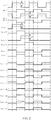
FIG. 2 is a schematic diagram of clock signals, gate drive signals, and charging voltages of pixel units of the first embodiment of the present disclosure. -
FIG. 3 is a schematic diagram of clock signals, gate drive signals, and charging voltages of pixel units of a second embodiment of the present disclosure. -
FIG. 4 is a schematic diagram of clock signals, gate drive signals, and charging voltages of pixel units of a third embodiment of the present disclosure. - The technical solutions in the embodiments of the present disclosure will be clearly and completely described below in combination with the accompanying drawings. Apparently, the embodiments in the following description are a part of the embodiments rather than all of the embodiments of the present disclosure. All other embodiments obtained by persons of ordinary skill in the art based on the embodiments of the present disclosure without making creative efforts shall fall within the protection scope of the present disclosure.
- Please refer to
FIG. 1 , which is a schematic diagram of a liquid crystal display panel of a first embodiment of the present disclosure. A liquid crystal display panel 30 includes a plurality of pixel units, such as Pixel11, Pixel12, Pixel13, Pixel14, Pixel21, Pixel22, Pixel23, Pixel24. These pixel units are arranged in an array. Agate drive circuit 31 is disposed on one side of the liquid crystal display panel 30, and includes afirst drive stage 311, asecond drive stage 312, athird drive stage 313, and afourth drive stage 314. Thegate drive circuit 31 is connected to a plurality of scan lines and is configured to sequentially provide gate drive signals on the plurality of scan lines to turn on the pixel units connected to the scan lines row by row. A scan line G1 is connected to thefirst drive stage 311, a scan line G2 is connected to thesecond drive stage 312, a scan line G3 is connected to thethird drive stage 313, and a scan line G4 is connected to thefourth drive stage 314. - Each two scan lines correspond to the pixel units arranged in the same row, and are alternately connected to the pixel units arranged in the same line. For example, the scan line G1 and the scan line G2 correspond to the pixel units Pixel11, Pixel12, Pixel21, and Pixel22 arranged in the same row. The scan line G1 is connected to the pixel unit Pixel11. The scan line G2 is connected to the pixel unit Pixel12 which is adjacent to in the same row as the pixel unit Pixel11. The scan line G1 is connected to the pixel unit Pixel21 which is adjacent to in the same row as the pixel unit Pixel12. The scan line G2 is connected to the pixel unit Pixel22 which is adjacent to in the same row as the pixel unit Pixel21.
- The
data drive circuit 32 is disposed on one side of the liquid crystal display panel 30 and connected to a plurality of data lines. Thedata drive circuit 32 is configured to charge the pixel units connected to the data lines and turned on by the drive of the gate drive signals. For example, a data line D1 is connected to a column of the pixel units Pixel11,Pixel 13, and a column of the pixel units Pixel12,Pixel 14 adjacent thereto. - The scan line G1, the scan line G2, the scan line G3, and the scan line G4 are perpendicular to data lines D1, D2, and D3, respectively. In other embodiments, the scan line G1, the scan line G2, the scan line G3, and the scan line G4 and the data lines D1, D2, and D3 are not necessarily perpendicular to each other, and they may have an included angle of any size.
- Please refer to
FIG. 2 , which is a pulse diagram of a charging result of pixel units of the first embodiment of the present disclosure. A signal CK1 is a first clock drive signal received by thefirst drive stage 311, a signal CK2 is a second clock drive signal received by thesecond drive stage 312, a signal CK3 is a third clock drive signal received by thethird drive stage 313, and a signal CK4 is a fourth clock drive signal received by thefourth drive stage 314. The signal CK1, the signal CK2, the signal CK3 and the signal CK4 have the same cycle, and their phases are sequentially shifted by a quarter of a cycle. A signal Gate1 is a first gate drive signal that thefirst drive stage 311 outputs to the gate line G1 according to the signal CK1. A signal Gate2 is a second gate drive signal that thesecond drive stage 312 outputs to the gate line G2 according to the signal CK2. A signal Gate3 is a third gate drive signal that thethird drive stage 313 outputs to the gate line G3 according to the signal CK3. A signal Gate4 is a fourth gate drive signal that thefourth drive stage 314 outputs to the gate line G4 according to the signal CK4. Cycles of the signal Gate1, the signal Gate2, the signal Gate3, and the signal Gate4 are the same, and their phases are sequentially shifted by a quarter of a cycle. Thepixel unit Pixel 11 connected to the gate line G1 is driven by the signal Gate1, The pixel unit Pixel12 connected to the gate line G2 is driven by the signal Gate2, The pixel unit Pixel13 connected to the gate line G3 is driven by the signal Gate3, and Thepixel unit Pixel 14 connected to the gate line G4 is driven by the signal Gate4. - The signal CK1 and the signal CK3 have the same pulse amplitude, the signal CK2 and the signal CK4 have the same pulse amplitude, and the pulse amplitude of the signal CK1 and the signal CK3 is ΔV greater than the pulse amplitude of the signal CK2 and the signal CK4. Thus, the signal Gate1 output according to the signal CK1 and the signal Gate3 output according to the signal CK3 have pulses of the same amplitude. The signal Gate2 output according to the signal CK2 and the signal Gate4 output according to the signal CK4 have pulses of the same amplitude. Therefore, the pulse amplitude of the signal Gate1 and the signal Gate3 is ΔV greater than the pulse amplitude of the signal Gate2 and the signal Gate4. The greater the pulse amplitudes of the gate drive signals, the better the driving performance on the pixel units, and the greater the charging efficiency of the pixel units. Accordingly, a charging efficiency of the
pixel units Pixel 11 andPixel 13 driven by the signal Gate1 and the signal Gate3 is greater than that ofpixel units Pixel 12 andPixel 14 driven by the signal Gate2 and the signal Gate4. - In this embodiment, the pulse amplitude of the signal CK1 and the signal CK3 is greater than the pulse amplitude of the signal CK2 and the signal CK4 by increasing the pulse amplitude of the signal CK1 and the signal CK3. In other embodiments, it can also be achieved by reducing the pulse amplitude of the signal CK2 and the signal CK4. Alternatively, it can also be achieved by increasing the pulse amplitude of the signal CK1 and the signal CK3 and reducing the pulse amplitude of the signal CK2 and the signal CK4.
- A signal Data1 is a data signal input to the data line D1 by the data drive
circuit 32, and a signal Data2 is a data signal input to the data line D2 by the data drivecircuit 32. The signals Data1 and Data2 have the same cycle and opposite polarity. - As shown in
FIG. 2 , thepixel unit Pixel 11 is driven to turn on by the signal Gate1 before a polarity of the signal Data1 is reversed. Thepixel unit Pixel 11 is charged with a high voltage received from the Data1 within a first quarter of a cycle when it is turned on. The pixel unit Pixel11 is charged with a low voltage received from the Data1 within the last quarter of the cycle when it is turned on under the driving of the Gate1. The polarity is reversed during charging, resulting in incomplete charging. After the polarity of the signal Data1 is reversed, the pixel unit Pixel12 is turned on under the driving of the signal Gate2. When the pixel unit Pixel2 is turned on, it is charged with the low voltage received from the Data1. There is no polarity reversion, and the charging is complete. - A charging efficiency of the
pixel unit Pixel 11 driven by the signal Gate1 is greater than that of the pixel unit Pixel12 driven by the signal Gate2. Therefore, although thepixel unit Pixel 11 undergoes polarity reversion during the charging process, a difference between charging amount of the pixel unit Pixel11 and thepixel unit Pixel 12 is small. - Similarly, the pixel unit Pixel13 is driven to turn on by the signal Gate3 before the polarity of the signal Data1 is inverted. The
pixel unit Pixel 13 is charged with the low voltage received from the Data1 within the first quarter of the cycle when it is turned on. The pixel unit Pixel13 is charged with the high voltage received from the Data1 within the last quarter of the cycle when it is turned on under the driving of the Gate3. The polarity is reversed during charging, resulting in incomplete charging. After the polarity of the signal Data1 is reversed, thepixel unit Pixel 14 is turned on under the driving of the signal Gate4. When the pixel unit Pixel3 is turned on, it is charged with the high voltage received from the Data1. There is no polarity reversion, and the charging is complete. - A charging efficiency of the pixel unit Pixel13 driven by the signal Gate3 is greater than that of the pixel unit Pixel14 driven by the signal Gate4. Therefore, although the pixel unit Pixel13 undergoes polarity reversion during the charging process, a difference between charging amount of the
pixel unit Pixel 13 and thepixel unit Pixel 14 is small. - A charging principle of the pixel units Pixel21, Pixel22, Pixel23 and Pixel24 is similar to that of the pixel units Pixel11, Pixel12, Pixel13, and Pixel14, and is not repeated here.
- In other embodiments, the gate drive circuit may further include six or eight or more drive stages, as long as the number of drive stages is even.
- From the above description, it can be known that in this embodiment, by increasing the voltage of the gate drive signals of the pixel units that will undergo polarity reversion when charging is performed, so as to increase the charging efficiency of these pixel units and to reduce the difference between the charging amount of these pixel units that undergo polarity reversion during charging such that the difference between the charging amount of pixel units that undergoes polarity reversion during charging and the charging amount of pixel units that do not undergo polarity reversion during charging is reduced, thereby reducing a difference in brightness of a screen and improving a display performance.
- Please refer to
FIG. 1 andFIG. 3, FIG. 3 is a pulse diagram of a charging result of pixel units of a second embodiment of the present disclosure. A signal CK1 is a first clock drive signal received by thefirst drive stage 311, a signal CK2 is a second clock drive signal received by thesecond drive stage 312, a signal CK3 is a third clock drive signal received by thethird drive stage 313, and a signal CK4 is a fourth clock drive signal received by thefourth drive stage 314. The signal CK1, the signal CK2, the signal CK3, and the signal CK4 have the same cycle, and their phases are sequentially shifted by a quarter of a cycle. A signal Gate1 is a first gate drive signal that thefirst drive stage 311 outputs to the gate line G1 according to the signal CK1. A signal Gate2 is a second gate drive signal that thesecond drive stage 312 outputs to the gate line G2 according to the signal CK2. A signal Gate3 is a third gate drive signal that thethird drive stage 313 outputs to the gate line G3 according to the signal CK3. A signal Gate4 is a fourth gate drive signal that thefourth drive stage 314 outputs to the gate line G4 according to the signal CK4. Cycles of the signal Gate1, the signal Gate2, the signal Gate3, and the signal Gate4 are the same, and their phases are sequentially shifted by a quarter of a cycle. Thepixel unit Pixel 11 connected to the gate line G1 is driven by the signal Gate1, The pixel unit Pixel12 connected to the gate line G2 is driven by the signal Gate2, Thepixel unit Pixel 13 connected to the gate line G3 is driven by the signal Gate3, and Thepixel unit Pixel 14 connected to the gate line G4 is driven by the signal Gate4. - The signal CK1 and the signal CK3 have the same pulse amplitude, the signal CK2 and the signal CK4 have the same pulse amplitude, and the second half of the pulse amplitude of the signal CK1 and the signal CK3 is ΔV greater than that of the signal CK2 and the signal CK4. Thus, the signal Gate1 output according to the signal CK1 and the signal Gate3 output according to the signal CK3 have pulses of the same amplitude. The signal Gate2 output according to the signal CK2 and the signal Gate4 output according to the signal CK4 have pulses of the same amplitude. Therefore, the second half of the pulse amplitude of the signal CK1 and the signal CK3 is ΔV greater than that of the signal CK2 and the signal CK4. The greater the pulse amplitudes of the gate drive signals, the better the driving performance on the pixel units, and the greater the charging efficiency of the pixel units. Accordingly, a charging efficiency of the pixel units Pixel11 and Pixel13 driven by the signal Gate1 and the signal Gate3 is greater than that of
pixel units Pixel 12 andPixel 14 driven by the signal Gate2 and the signal Gate4. - In this embodiment, by increasing the second half of the pulse amplitude of the signal CK1 and the signal CK3, the pulse amplitude of the signal CK1 and the signal CK3 is greater than the pulse amplitude of the signal CK2 and the signal CK4. In other embodiments, the pulse amplitude of the signal CK2 and the signal CK4 can also be reduced. Alternatively, it can be achieved by increasing the pulse amplitude of the second half of the signal CK1 and the signal CK3 and decreasing the pulse amplitude of the signal CK2 and the signal CK4.
- In other embodiments, a proportion of time occupied by high pulses of the signal CK1 and the signal CK3 may be any proportion, and it is not limited to a 50% proportion as shown in
FIG. 3 . - A signal Data1 is a data signal input to the data line D1 by the data drive
circuit 32, and a signal Data2 is a data signal input to the data line D2 by the data drivecircuit 32. The signals Data1 and Data2 have the same cycle and opposite polarity. - As shown in
FIG. 3 , the pixel unit Pixel11 is driven to turn on by the signal Gate1 before a polarity of the signal Data1 is reversed. The pixel unit Pixel11 is charged with a high voltage received from the Data1 within a first quarter of a cycle when it is turned on. The pixel unit Pixel11 is charged with a low voltage received from the Data1 within the last quarter of the cycle when it is turned on under the driving of the Gate1. The polarity is reversed during charging, resulting in incomplete charging. After the polarity of the signal Data1 is reversed, the pixel unit Pixel12 is turned on under the driving of the signal Gate2. When the pixel unit Pixel2 is turned on, it is charged with the low voltage received from the Data1. There is no polarity reversion, and the charging is complete. - A charging efficiency of the pixel unit Pixel11 driven by the signal Gate1 is greater than that of the pixel unit Pixel12 driven by the signal Gate2. Therefore, although the
pixel unit Pixel 11 undergoes polarity reversion during the charging process, a difference between charging amount of thepixel unit Pixel 11 and thepixel unit Pixel 12 is small. - Similarly, the pixel unit Pixel13 is driven to turn on by the signal Gate3 before the polarity of the signal Data1 is inverted. The
pixel unit Pixel 13 is charged with the low voltage received from the Data1 within the first quarter of the cycle when it is turned on. The pixel unit Pixel13 is charged with the high voltage received from the Data1 within the last quarter of the cycle when it is turned on under the driving of the Gate3. The polarity is reversed during charging, resulting in incomplete charging. After the polarity of the signal Data1 is reversed, thepixel unit Pixel 14 is turned on under the driving of the signal Gate4. When the pixel unit Pixel3 is turned on, it is charged with the high voltage received from the Data1. There is no polarity reversion, and the charging is complete. - A charging efficiency of the pixel unit Pixel13 driven by the signal Gate3 is greater than that of the pixel unit Pixel14 driven by the signal Gate4. Therefore, although the pixel unit Pixel13 undergoes polarity reversion during the charging process, a difference between charging amount of the
pixel unit Pixel 13 and thepixel unit Pixel 14 is small. - A charging principle of the pixel units Pixel21, Pixel22, Pixel23 and Pixel24 is similar to that of the pixel units Pixel11, Pixel12, Pixel13, and Pixel14, and is not repeated here.
- Please refer to
FIG. 1 andFIG. 4, FIG. 4 is a pulse diagram of a charging result of pixel units of a third embodiment of the present disclosure. A signal CK1 is a first clock drive signal received by thefirst drive stage 311, a signal CK2 is a second clock drive signal received by thesecond drive stage 312, a signal CK3 is a third clock drive signal received by thethird drive stage 313, and a signal CK4 is a fourth clock drive signal received by thefourth drive stage 314. The signal CK1, the signal CK2, the signal CK3, and the signal CK4 have the same cycle, and their phases are sequentially shifted by a quarter of a cycle. A signal Gate1 is a first gate drive signal that thefirst drive stage 311 outputs to the gate line G1 according to the signal CK1. A signal Gate2 is a second gate drive signal that thesecond drive stage 312 outputs to the gate line G2 according to the signal CK2. A signal Gate3 is a third gate drive signal that thethird drive stage 313 outputs to the gate line G3 according to the signal CK3. A signal Gate4 is a fourth gate drive signal that thefourth drive stage 314 outputs to the gate line G4 according to the signal CK4. Cycles of the signal Gate1, the signal Gate2, the signal Gate3, and the signal Gate4 are the same, and their phases are sequentially shifted by a quarter of a cycle. Thepixel unit Pixel 11 connected to the gate line G1 is driven by the signal Gate1, The pixel unit Pixel12 connected to the gate line G2 is driven by the signal Gate2, Thepixel unit Pixel 13 connected to the gate line G3 is driven by the signal Gate3, and Thepixel unit Pixel 14 connected to the gate line G4 is driven by the signal Gate4. - The signal CK1 and the signal CK3 have the same pulse width, the signal CK2 and the signal CK4 have the same pulse width, and the pulse width of the signal CK1 and the signal CK3 is greater than the pulse width of the signal CK2 and the signal CK4. Thus, the signal Gate1 output according to the signal CK1 and the signal Gate3 output according to the signal CK3 have the same pulse width. The signal Gate2 output according to the signal CK2 and the signal Gate4 output according to the signal CK4 have the same pulse width. Also, the pulse width of the signal CK1 and the signal CK3 is greater than the pulse width of the signal CK2 and the signal CK4. The greater the pulse widths of the gate drive signals, the longer the charging time of the pixel units, and the more power each pixel unit charges. Accordingly, a charging time of the pixel units Pixel11 and
Pixel 13 driven by the signal Gate1 and the signal Gate3 is longer than a charging time of the pixel units Pixel12 and Pixel14 driven by the signal Gate2 and the signal Gate4. - In this embodiment, by increasing the pulse width of the signal CK1 and the signal CK3 and decreasing the pulse width of the signal CK2 and the signal CK4, the pulse width of the signal CK1 and the signal CK3 is greater than the pulse width of the signal CK2 and the signal CK4. In other embodiments, the pulse width of the signal CK2 and the signal CK4 can also be reduced. Alternatively, the pulse width of the signal CK1 and the signal CK3 can also be increased.
- A signal Data1 is a data signal input to the data line D1 by the data drive
circuit 32, and a signal Data2 is a data signal input to the data line D2 by the data drivecircuit 32. The signals Data1 and Data2 have the same cycle and opposite polarity. - As shown in
FIG. 4 , the pixel unit Pixel11 is driven to turn on by the signal Gate1 before a polarity of the signal Data1 is reversed. The pixel unit Pixel11 is charged with a high voltage received from the Data1 within a first quarter of a cycle when it is turned on. Thepixel unit Pixel 11 is charged with a low voltage received from the Data1 within the last quarter of the cycle when it is turned on under the driving of the Gate1. The polarity is reversed during charging, resulting in incomplete charging. After the polarity of the signal Data1 is reversed, the pixel unit Pixel12 is turned on under the driving of the signal Gate2. When the pixel unit Pixel2 is turned on, it is charged with the low voltage received from the Data1. There is no polarity reversion, and the charging is complete. However, the pulse width of the signal Gate1 is large, so the pixel unit Pixel11 has a longer time to charge after the polarity is reversed, which can charge more power. The pulse width of the signal Gate2 is smaller, so the charging time of thepixel unit Pixel 12 is shorter, and the charging power is smaller. Therefore, the difference between the charging amount of thepixel unit Pixel 11 and thepixel unit Pixel 12 is small. - Similarly, the pixel unit Pixel13 is driven to turn on by the signal Gate3. The pixel unit Pixel13 is charged with the low voltage received from the Data1 within the first quarter of the cycle when it is turned on. The pixel unit Pixel13 is charged with the high voltage received from the Data1 within the last quarter of the cycle when it is turned on under the driving of the Gate3. The polarity is reversed during charging, resulting in incomplete charging. The pixel unit Pixel14 is turned on under the driving of the signal Gate4. When the pixel unit Pixel14 is turned on, it is charged with the high voltage received from the Data1. There is no polarity reversion, and the charging is complete.
- However, the pulse width of the signal Gate3 is large, so the pixel unit Pixel13 has a longer time to charge after the polarity is reversed, which can charge more power. The pulse width of the signal Gate4 is smaller, so the charging time of the pixel unit Pixel14 is shorter, and the charging power is smaller. Therefore, the difference between the charging amount of the
pixel unit Pixel 13 and thepixel unit Pixel 14 is small. - A charging principle of the pixel units Pixel21, Pixel22, Pixel23 and Pixel24 is similar to that of the pixel units Pixel11, Pixel12, Pixel13, and Pixel14, and is not repeated here.
- In other embodiments, the gate drive circuit may further include six or eight or more drive stages, as long as the number of drive stages is even.
- From the above description, it can be known that in this embodiment, by extending the pulse width of the gate drive signals of pixel units that will undergo polarity reversion during charging, the charging time of these pixel units will be extended such that the difference between the charging amount of pixel units that undergoes polarity reversion during charging and the charging amount of pixel units that do not undergo polarity reversion during charging is reduced, thereby reducing a difference in brightness of a screen and improving a display performance.
- A difference between the prior art and the liquid crystal display panel of the present disclosure is that the gate drive signals on the two scan lines connected to the pixel units arranged in the same row have different driving capabilities, so the difference between the charging amount of pixel units that undergoes polarity reversion during charging and the charging amount of pixel units that do not undergo polarity reversion during charging is reduced, thereby reducing a difference in brightness of a screen and improving a display performance.
- The above description is only the preferable embodiments of the present disclosure and is not intended to limit the scope of the present disclosure. All conversions of equivalents structures and equivalents procedures made by using the description and accompanying drawings of the present disclosure, or direct or indirect using in other related technical field, should be embodied in the protection scope of the appending claims of the present disclosure.
Claims (19)
- A liquid crystal display panel, comprising:a plurality of pixel units arranged in an array;a plurality of scan lines, wherein each two of the scan lines correspond to pixel units arranged in the same row and are alternately connected to the pixel units arranged in the same row;a gate drive circuit configured to provide a plurality of gate drive signals on one scan line sequentially to turn on pixel units connected to the scan line;a plurality of data lines arranged next to each column of the pixel units, wherein each data line is connected to the pixel units of two adjacent columns; anda data drive circuit configured to provide a plurality of data drive signals to the data lines in a polarity reversal manner to charge the pixel units connected to the data lines and being turned on;wherein corresponding to the pixel units arranged in the same row, the pixel units connected to a first scan line of the two scan lines are turned on before a polarity of the data drive signals is reversed, and the pixel units connected to a second scan line of the two scan lines are turned on after or at the same time as the polarity of the data drive signals is reversed; and wherein a driving capability of the gate drive signals on the first scan line is greater than a driving capability of the gate drive signals on the second scan line, thereby eliminating a charging difference caused by the polarity reversion of the data drive signals; andwherein the gate drive signals on the plurality of scan lines are sequentially shifted by a quarter of a polarity reversal cycle of the data drive signals along a column direction.
- The liquid crystal display panel as claimed in claim 1, wherein a pulse height of the gate drive signals on the first scan line is at least partially greater than a pulse height of the gate drive signals on the second scan line.
- The liquid crystal display panel as claimed in claim 1, wherein a pulse width of the gate drive signals on the first scan line is greater than a pulse width of the gate drive signals on the second scan line.
- The liquid crystal display panel as claimed in claim 1, wherein the gate drive circuit is disposed on one side of the liquid crystal display panel.
- The liquid crystal display panel as claimed in claim 1, wherein the data drive circuit is disposed on another side of the liquid crystal display panel.
- The liquid crystal display panel as claimed in claim 1, wherein the plurality of scan lines are perpendicular to the plurality of data lines.
- A liquid crystal display panel, comprising:a plurality of pixel units arranged in an array;a plurality of scan lines, wherein each two of the scan lines correspond to pixel units arranged in the same row and are alternately connected to the pixel units arranged in the same row;a gate drive circuit configured to provide a plurality of gate drive signals on one scan line sequentially to turn on pixel units connected to the scan line;a plurality of data lines arranged next to each column of the pixel units, wherein each data line is connected to the pixel units of two adjacent columns; anda data drive circuit configured to provide a plurality of data drive signals to the data lines in a polarity reversal manner to charge the pixel units connected to the data lines and being turned on;wherein the gate drive signals on the two scan lines corresponding to the pixel units arranged in the same row have different driving capabilities, thereby eliminating a charging difference caused by a polarity reversion of the data drive signals.
- The liquid crystal display panel as claimed in claim 7, wherein corresponding to the pixel units arranged in the same row, the pixel units connected to a first scan line of the two scan lines are turned on before a polarity of the data drive signals is reversed, and the pixel units connected to a second scan line of the two scan lines are turned on after or at the same time as the polarity of the data drive signals is reversed, and a driving capability of the gate drive signals on the first scan line is greater than a driving capability of the gate drive signals on the second scan line.
- The liquid crystal display panel as claimed in claim 8, wherein a pulse height of the gate drive signals on the first scan line is at least partially greater than a pulse height of the gate drive signals on the second scan line.
- The liquid crystal display panel as claimed in claim 8, wherein a pulse width of the gate drive signals on the first scan line is greater than a pulse width of the gate drive signals on the second scan line.
- The liquid crystal display panel as claimed in claim 7, wherein the gate drive signals on the plurality of scan lines are sequentially shifted by a quarter of a polarity reversal cycle of the data drive signals along a column direction.
- The liquid crystal display panel as claimed in claim 7, wherein the gate drive circuit is disposed on one side of the liquid crystal display panel.
- The liquid crystal display panel as claimed in claim 7, wherein the data drive circuit is disposed on another side of the liquid crystal display panel.
- The liquid crystal display panel as claimed in claim 7, wherein the plurality of scan lines are perpendicular to the plurality of data lines.
- A gate drive circuit mounted on a liquid crystal display panel, comprising a first drive stage and a second drive stage, wherein the first drive stage receives a first clock signal, and outputs a first gate drive signal in response to the first clock signal, the second drive stage receives a second clock signal, and outputs a second gate drive signal in response to the second clock signal, wherein the first clock signal and the second clock signal are set such that a driving capability of the first gate drive signal is different from a driving capability of the second gate drive signal.
- The gate drive circuit as claimed in claim 15, wherein a pulse amplitude of the first clock signal is greater than a pulse amplitude of the second clock signal, so that a pulse amplitude of the first gate drive signal is greater than a pulse amplitude of the second gate drive signal.
- The gate drive circuit as claimed in claim 15, wherein a pulse width of the first clock signal is greater than a pulse width of the second clock signal, so that a pulse width of the first gate drive signal is greater than a pulse width of the second gate drive signal.
- The gate drive circuit as claimed in claim 15, further comprising a third drive stage and a fourth drive stage, wherein the third drive stage receives a third clock signal, and outputs a third gate drive signal in response to the third clock signal, the fourth drive stage receives a fourth clock signal, and outputs a fourth gate drive signal in response to the fourth clock signal, wherein the third clock signal and the fourth clock signal are further set such that a driving capability of the third gate drive signal is the same as the driving capability of the first gate drive signal, and a driving capability of the fourth gate drive signal is the same as the driving capability of the second gate drive signal.
- The gate drive circuit as claimed in claim 18, wherein a cycle from the first clock signal to the fourth clock signal is the same and phases of each other are sequentially shifted by a quarter of the cycle, so that a cycle from the first gate drive signal to the fourth gate drive signal is the same and phases of each other are sequentially shifted by a quarter of the cycle.
Applications Claiming Priority (2)
| Application Number | Priority Date | Filing Date | Title |
|---|---|---|---|
| CN201711088166.3A CN107767832B (en) | 2017-11-07 | 2017-11-07 | Liquid crystal display panel and grid drive circuit |
| PCT/CN2017/117313 WO2019090908A1 (en) | 2017-11-07 | 2017-12-20 | Liquid crystal display panel and gate drive circuit |
Publications (2)
| Publication Number | Publication Date |
|---|---|
| EP3709286A1 true EP3709286A1 (en) | 2020-09-16 |
| EP3709286A4 EP3709286A4 (en) | 2021-09-01 |
Family
ID=61272742
Family Applications (1)
| Application Number | Title | Priority Date | Filing Date |
|---|---|---|---|
| EP17931182.4A Withdrawn EP3709286A4 (en) | 2017-11-07 | 2017-12-20 | LIQUID CRYSTAL DISPLAY PANEL AND GRID ATTACK CIRCUIT |
Country Status (6)
| Country | Link |
|---|---|
| US (1) | US10475408B2 (en) |
| EP (1) | EP3709286A4 (en) |
| JP (1) | JP2020535470A (en) |
| KR (1) | KR20200075004A (en) |
| CN (1) | CN107767832B (en) |
| WO (1) | WO2019090908A1 (en) |
Cited By (1)
| Publication number | Priority date | Publication date | Assignee | Title |
|---|---|---|---|---|
| CN116682380A (en) * | 2023-06-12 | 2023-09-01 | 惠科股份有限公司 | Data driving circuit, display panel, driving strength adjustment method and storage medium |
Families Citing this family (18)
| Publication number | Priority date | Publication date | Assignee | Title |
|---|---|---|---|---|
| CN108877722B (en) * | 2018-07-27 | 2020-12-01 | 京东方科技集团股份有限公司 | Gate driving unit group and driving method thereof, gate driving circuit and display device |
| KR20260053047A (en) | 2018-09-21 | 2026-04-20 | 가부시키가이샤 한도오따이 에네루기 켄큐쇼 | Flip-flop circuit, driver circuit, display panel, display device, input/output device, and information processing device |
| CN109410867B (en) | 2018-12-05 | 2020-10-16 | 惠科股份有限公司 | Display panel, driving method and display device |
| CN109448649A (en) * | 2018-12-17 | 2019-03-08 | 惠科股份有限公司 | Display panel, driving method of display panel and display device |
| CN109584837A (en) * | 2019-01-30 | 2019-04-05 | 惠科股份有限公司 | Display panel driving method and display device |
| CN109584838A (en) * | 2019-01-30 | 2019-04-05 | 惠科股份有限公司 | Display panel driving method and display device |
| CN109616072A (en) * | 2019-01-30 | 2019-04-12 | 惠科股份有限公司 | Display panel driving method and display device |
| CN109671408A (en) * | 2019-01-30 | 2019-04-23 | 惠科股份有限公司 | Driving method, device and equipment of display panel and storage medium |
| CN109599075B (en) | 2019-01-30 | 2020-12-15 | 惠科股份有限公司 | Driving method and driving device of display panel and display equipment |
| CN109584840B (en) * | 2019-01-30 | 2020-12-29 | 惠科股份有限公司 | Driving method and device of display panel |
| CN109658893B (en) * | 2019-01-30 | 2021-05-28 | 惠科股份有限公司 | Driving method and driving device of display panel and display equipment |
| CN109686304B (en) * | 2019-02-20 | 2020-09-01 | 深圳市华星光电半导体显示技术有限公司 | Display panel and driving method thereof |
| CN112017600B (en) * | 2019-05-30 | 2022-02-01 | 京东方科技集团股份有限公司 | Driving device and method of liquid crystal display panel and display device |
| CN110767186A (en) * | 2019-09-29 | 2020-02-07 | 福建华佳彩有限公司 | Driving method of dual-gate panel |
| CN112731719A (en) * | 2020-12-31 | 2021-04-30 | 重庆惠科金渝光电科技有限公司 | Display panel, driving method thereof, and computer storage medium |
| CN114203128B (en) * | 2021-12-17 | 2022-11-15 | 武汉京东方光电科技有限公司 | Display panel driving method and circuit and display device |
| WO2024000462A1 (en) * | 2022-06-30 | 2024-01-04 | 京东方科技集团股份有限公司 | Display substrate and display apparatus |
| CN116486730B (en) * | 2023-04-26 | 2026-05-12 | 京东方科技集团股份有限公司 | Display module, driving method thereof and display device |
Family Cites Families (19)
| Publication number | Priority date | Publication date | Assignee | Title |
|---|---|---|---|---|
| TW552573B (en) * | 2001-08-21 | 2003-09-11 | Samsung Electronics Co Ltd | Liquid crystal display and driving method thereof |
| US7369111B2 (en) * | 2003-04-29 | 2008-05-06 | Samsung Electronics Co., Ltd. | Gate driving circuit and display apparatus having the same |
| JP2006177992A (en) * | 2004-12-20 | 2006-07-06 | Mitsubishi Electric Corp | Method for driving liquid crystal display device and liquid crystal display device |
| US7586476B2 (en) * | 2005-06-15 | 2009-09-08 | Lg. Display Co., Ltd. | Apparatus and method for driving liquid crystal display device |
| US20070004079A1 (en) * | 2005-06-30 | 2007-01-04 | Geefay Frank S | Method for making contact through via contact to an offset contactor inside a cap for the wafer level packaging of FBAR chips |
| KR101158899B1 (en) * | 2005-08-22 | 2012-06-25 | 삼성전자주식회사 | Liquid crystal display device, and method for driving thereof |
| JP4201026B2 (en) * | 2006-07-07 | 2008-12-24 | ソニー株式会社 | Liquid crystal display device and driving method of liquid crystal display device |
| KR101375863B1 (en) * | 2007-03-08 | 2014-03-17 | 삼성디스플레이 주식회사 | Display apparatus and method of driving the same |
| CN100562780C (en) * | 2007-09-04 | 2009-11-25 | 友达光电股份有限公司 | Double-side grid driving type liquid crystal display and its driving method |
| JP5100450B2 (en) * | 2007-11-29 | 2012-12-19 | 三菱電機株式会社 | Image display apparatus and driving method thereof |
| CN101676985A (en) | 2008-09-17 | 2010-03-24 | 北京京东方光电科技有限公司 | Liquid crystal display signal inversion driving method |
| US20130057598A1 (en) * | 2010-06-02 | 2013-03-07 | Akihisa Iwamoto | Display panel, display device, and method of driving the same |
| TWI489437B (en) * | 2010-06-02 | 2015-06-21 | Novatek Microelectronics Corp | Driving method driving module and liquid crystal display device |
| JP2012068599A (en) * | 2010-09-27 | 2012-04-05 | Casio Comput Co Ltd | Liquid crystal display device |
| KR20120075166A (en) * | 2010-12-28 | 2012-07-06 | 삼성모바일디스플레이주식회사 | Lcd display device and driving method thereof |
| CN102237034B (en) * | 2011-07-11 | 2013-05-08 | 北京大学深圳研究生院 | Grid driving circuit and display device |
| JP2014153541A (en) * | 2013-02-08 | 2014-08-25 | Japan Display Central Co Ltd | Image display unit and driving method of the same |
| CN105489185B (en) * | 2016-01-25 | 2017-12-01 | 京东方科技集团股份有限公司 | Driving device, display device and driving method |
| CN206946910U (en) * | 2017-11-07 | 2018-01-30 | 深圳市华星光电半导体显示技术有限公司 | A kind of liquid crystal display panel |
-
2017
- 2017-11-07 CN CN201711088166.3A patent/CN107767832B/en not_active Expired - Fee Related
- 2017-12-20 JP JP2020517338A patent/JP2020535470A/en active Pending
- 2017-12-20 US US15/742,504 patent/US10475408B2/en not_active Expired - Fee Related
- 2017-12-20 KR KR1020207015952A patent/KR20200075004A/en not_active Ceased
- 2017-12-20 WO PCT/CN2017/117313 patent/WO2019090908A1/en not_active Ceased
- 2017-12-20 EP EP17931182.4A patent/EP3709286A4/en not_active Withdrawn
Cited By (1)
| Publication number | Priority date | Publication date | Assignee | Title |
|---|---|---|---|---|
| CN116682380A (en) * | 2023-06-12 | 2023-09-01 | 惠科股份有限公司 | Data driving circuit, display panel, driving strength adjustment method and storage medium |
Also Published As
| Publication number | Publication date |
|---|---|
| WO2019090908A1 (en) | 2019-05-16 |
| US20190139507A1 (en) | 2019-05-09 |
| JP2020535470A (en) | 2020-12-03 |
| CN107767832B (en) | 2020-02-07 |
| KR20200075004A (en) | 2020-06-25 |
| EP3709286A4 (en) | 2021-09-01 |
| CN107767832A (en) | 2018-03-06 |
| US10475408B2 (en) | 2019-11-12 |
Similar Documents
| Publication | Publication Date | Title |
|---|---|---|
| CN107767832B (en) | Liquid crystal display panel and grid drive circuit | |
| US20240212550A1 (en) | Display panel, display device and driving method | |
| US10242634B2 (en) | Display device | |
| US9799283B2 (en) | HSD liquid crystal display panel, display device and driving method thereof | |
| CN102799036B (en) | A kind of display and display panel | |
| US8330695B2 (en) | Liquid crystal display device, method for driving the same, and television receiver | |
| US10332471B2 (en) | Pulse generation device, array substrate, display device, drive circuit and driving method | |
| CN1753072A (en) | Liquid crystal display device and method of driving the same | |
| US20230059832A1 (en) | Display panel and display device | |
| US10942405B2 (en) | Display device | |
| CN109559706B (en) | Display driving circuit and display device | |
| US8581822B2 (en) | Double-gate liquid crystal display device which adjusts main-charge time and precharge time according to data polarities and related driving method | |
| US12014699B2 (en) | Display panel, display panel driving method, and display device | |
| WO2017101573A1 (en) | Pixel circuit, driving method therefor, driver circuit, and display device | |
| CN103474039A (en) | Grid line driving method, grid driving circuit and display device | |
| WO2020233549A1 (en) | Array substrate and driving method thereof, and display device | |
| CN117524166A (en) | Display panel and display device | |
| CN110879500B (en) | Display substrate, driving method thereof, display panel, display device | |
| TW201312535A (en) | LCD panel with the dual gate structure and the driving method of the same | |
| CN103293732B (en) | Liquid crystal panel drive method and liquid crystal panel | |
| US10134350B2 (en) | Shift register unit, method for driving same, gate driving circuit and display apparatus | |
| CN101710476B (en) | Display panel | |
| CN101551983A (en) | Buffer applied to source electrode driving circuit of display and control method thereof | |
| KR20130011265A (en) | Liquid crystal display device and method for driving the same | |
| CN101303835A (en) | Method for driving a liquid crystal display panel |
Legal Events
| Date | Code | Title | Description |
|---|---|---|---|
| STAA | Information on the status of an ep patent application or granted ep patent |
Free format text: STATUS: THE INTERNATIONAL PUBLICATION HAS BEEN MADE |
|
| PUAI | Public reference made under article 153(3) epc to a published international application that has entered the european phase |
Free format text: ORIGINAL CODE: 0009012 |
|
| STAA | Information on the status of an ep patent application or granted ep patent |
Free format text: STATUS: REQUEST FOR EXAMINATION WAS MADE |
|
| 17P | Request for examination filed |
Effective date: 20200519 |
|
| AK | Designated contracting states |
Kind code of ref document: A1 Designated state(s): AL AT BE BG CH CY CZ DE DK EE ES FI FR GB GR HR HU IE IS IT LI LT LU LV MC MK MT NL NO PL PT RO RS SE SI SK SM TR |
|
| AX | Request for extension of the european patent |
Extension state: BA ME |
|
| DAV | Request for validation of the european patent (deleted) | ||
| DAX | Request for extension of the european patent (deleted) | ||
| A4 | Supplementary search report drawn up and despatched |
Effective date: 20210802 |
|
| RIC1 | Information provided on ipc code assigned before grant |
Ipc: G09G 3/36 20060101AFI20210727BHEP |
|
| STAA | Information on the status of an ep patent application or granted ep patent |
Free format text: STATUS: THE APPLICATION IS DEEMED TO BE WITHDRAWN |
|
| 18D | Application deemed to be withdrawn |
Effective date: 20230701 |