EP3709175B1 - Speichervorrichtung und rechenvorrichtung mit der speichervorrichtung - Google Patents
Speichervorrichtung und rechenvorrichtung mit der speichervorrichtung Download PDFInfo
- Publication number
- EP3709175B1 EP3709175B1 EP20150631.8A EP20150631A EP3709175B1 EP 3709175 B1 EP3709175 B1 EP 3709175B1 EP 20150631 A EP20150631 A EP 20150631A EP 3709175 B1 EP3709175 B1 EP 3709175B1
- Authority
- EP
- European Patent Office
- Prior art keywords
- memory blocks
- storage device
- data
- memory
- buffer area
- Prior art date
- Legal status (The legal status is an assumption and is not a legal conclusion. Google has not performed a legal analysis and makes no representation as to the accuracy of the status listed.)
- Active
Links
Images








Classifications
-
- G—PHYSICS
- G06—COMPUTING OR CALCULATING; COUNTING
- G06F—ELECTRIC DIGITAL DATA PROCESSING
- G06F3/00—Input arrangements for transferring data to be processed into a form capable of being handled by the computer; Output arrangements for transferring data from processing unit to output unit, e.g. interface arrangements
- G06F3/06—Digital input from, or digital output to, record carriers, e.g. RAID, emulated record carriers or networked record carriers
- G06F3/0601—Interfaces specially adapted for storage systems
- G06F3/0602—Interfaces specially adapted for storage systems specifically adapted to achieve a particular effect
- G06F3/0614—Improving the reliability of storage systems
-
- G—PHYSICS
- G06—COMPUTING OR CALCULATING; COUNTING
- G06F—ELECTRIC DIGITAL DATA PROCESSING
- G06F12/00—Accessing, addressing or allocating within memory systems or architectures
- G06F12/02—Addressing or allocation; Relocation
- G06F12/0223—User address space allocation, e.g. contiguous or non contiguous base addressing
- G06F12/023—Free address space management
- G06F12/0238—Memory management in non-volatile memory, e.g. resistive RAM or ferroelectric memory
- G06F12/0246—Memory management in non-volatile memory, e.g. resistive RAM or ferroelectric memory in block erasable memory, e.g. flash memory
-
- G—PHYSICS
- G06—COMPUTING OR CALCULATING; COUNTING
- G06F—ELECTRIC DIGITAL DATA PROCESSING
- G06F3/00—Input arrangements for transferring data to be processed into a form capable of being handled by the computer; Output arrangements for transferring data from processing unit to output unit, e.g. interface arrangements
- G06F3/06—Digital input from, or digital output to, record carriers, e.g. RAID, emulated record carriers or networked record carriers
- G06F3/0601—Interfaces specially adapted for storage systems
- G06F3/0602—Interfaces specially adapted for storage systems specifically adapted to achieve a particular effect
- G06F3/0614—Improving the reliability of storage systems
- G06F3/0619—Improving the reliability of storage systems in relation to data integrity, e.g. data losses, bit errors
-
- G—PHYSICS
- G06—COMPUTING OR CALCULATING; COUNTING
- G06F—ELECTRIC DIGITAL DATA PROCESSING
- G06F3/00—Input arrangements for transferring data to be processed into a form capable of being handled by the computer; Output arrangements for transferring data from processing unit to output unit, e.g. interface arrangements
- G06F3/06—Digital input from, or digital output to, record carriers, e.g. RAID, emulated record carriers or networked record carriers
- G06F3/0601—Interfaces specially adapted for storage systems
- G06F3/0602—Interfaces specially adapted for storage systems specifically adapted to achieve a particular effect
- G06F3/0604—Improving or facilitating administration, e.g. storage management
-
- G—PHYSICS
- G06—COMPUTING OR CALCULATING; COUNTING
- G06F—ELECTRIC DIGITAL DATA PROCESSING
- G06F3/00—Input arrangements for transferring data to be processed into a form capable of being handled by the computer; Output arrangements for transferring data from processing unit to output unit, e.g. interface arrangements
- G06F3/06—Digital input from, or digital output to, record carriers, e.g. RAID, emulated record carriers or networked record carriers
- G06F3/0601—Interfaces specially adapted for storage systems
- G06F3/0602—Interfaces specially adapted for storage systems specifically adapted to achieve a particular effect
- G06F3/0608—Saving storage space on storage systems
-
- G—PHYSICS
- G06—COMPUTING OR CALCULATING; COUNTING
- G06F—ELECTRIC DIGITAL DATA PROCESSING
- G06F3/00—Input arrangements for transferring data to be processed into a form capable of being handled by the computer; Output arrangements for transferring data from processing unit to output unit, e.g. interface arrangements
- G06F3/06—Digital input from, or digital output to, record carriers, e.g. RAID, emulated record carriers or networked record carriers
- G06F3/0601—Interfaces specially adapted for storage systems
- G06F3/0602—Interfaces specially adapted for storage systems specifically adapted to achieve a particular effect
- G06F3/061—Improving I/O performance
- G06F3/0613—Improving I/O performance in relation to throughput
-
- G—PHYSICS
- G06—COMPUTING OR CALCULATING; COUNTING
- G06F—ELECTRIC DIGITAL DATA PROCESSING
- G06F3/00—Input arrangements for transferring data to be processed into a form capable of being handled by the computer; Output arrangements for transferring data from processing unit to output unit, e.g. interface arrangements
- G06F3/06—Digital input from, or digital output to, record carriers, e.g. RAID, emulated record carriers or networked record carriers
- G06F3/0601—Interfaces specially adapted for storage systems
- G06F3/0628—Interfaces specially adapted for storage systems making use of a particular technique
- G06F3/0638—Organizing or formatting or addressing of data
- G06F3/064—Management of blocks
-
- G—PHYSICS
- G06—COMPUTING OR CALCULATING; COUNTING
- G06F—ELECTRIC DIGITAL DATA PROCESSING
- G06F3/00—Input arrangements for transferring data to be processed into a form capable of being handled by the computer; Output arrangements for transferring data from processing unit to output unit, e.g. interface arrangements
- G06F3/06—Digital input from, or digital output to, record carriers, e.g. RAID, emulated record carriers or networked record carriers
- G06F3/0601—Interfaces specially adapted for storage systems
- G06F3/0628—Interfaces specially adapted for storage systems making use of a particular technique
- G06F3/0655—Vertical data movement, i.e. input-output transfer; data movement between one or more hosts and one or more storage devices
- G06F3/0656—Data buffering arrangements
-
- G—PHYSICS
- G06—COMPUTING OR CALCULATING; COUNTING
- G06F—ELECTRIC DIGITAL DATA PROCESSING
- G06F3/00—Input arrangements for transferring data to be processed into a form capable of being handled by the computer; Output arrangements for transferring data from processing unit to output unit, e.g. interface arrangements
- G06F3/06—Digital input from, or digital output to, record carriers, e.g. RAID, emulated record carriers or networked record carriers
- G06F3/0601—Interfaces specially adapted for storage systems
- G06F3/0628—Interfaces specially adapted for storage systems making use of a particular technique
- G06F3/0655—Vertical data movement, i.e. input-output transfer; data movement between one or more hosts and one or more storage devices
- G06F3/0658—Controller construction arrangements
-
- G—PHYSICS
- G06—COMPUTING OR CALCULATING; COUNTING
- G06F—ELECTRIC DIGITAL DATA PROCESSING
- G06F3/00—Input arrangements for transferring data to be processed into a form capable of being handled by the computer; Output arrangements for transferring data from processing unit to output unit, e.g. interface arrangements
- G06F3/06—Digital input from, or digital output to, record carriers, e.g. RAID, emulated record carriers or networked record carriers
- G06F3/0601—Interfaces specially adapted for storage systems
- G06F3/0628—Interfaces specially adapted for storage systems making use of a particular technique
- G06F3/0655—Vertical data movement, i.e. input-output transfer; data movement between one or more hosts and one or more storage devices
- G06F3/0659—Command handling arrangements, e.g. command buffers, queues, command scheduling
-
- G—PHYSICS
- G06—COMPUTING OR CALCULATING; COUNTING
- G06F—ELECTRIC DIGITAL DATA PROCESSING
- G06F3/00—Input arrangements for transferring data to be processed into a form capable of being handled by the computer; Output arrangements for transferring data from processing unit to output unit, e.g. interface arrangements
- G06F3/06—Digital input from, or digital output to, record carriers, e.g. RAID, emulated record carriers or networked record carriers
- G06F3/0601—Interfaces specially adapted for storage systems
- G06F3/0668—Interfaces specially adapted for storage systems adopting a particular infrastructure
- G06F3/0671—In-line storage system
- G06F3/0673—Single storage device
- G06F3/0679—Non-volatile semiconductor memory device, e.g. flash memory, one time programmable memory [OTP]
-
- G—PHYSICS
- G06—COMPUTING OR CALCULATING; COUNTING
- G06F—ELECTRIC DIGITAL DATA PROCESSING
- G06F2212/00—Indexing scheme relating to accessing, addressing or allocation within memory systems or architectures
- G06F2212/72—Details relating to flash memory management
- G06F2212/7203—Temporary buffering, e.g. using volatile buffer or dedicated buffer blocks
Definitions
- the degree of integration of the storage device and a volume thereof continues to increase as semiconductor manufacturing technologies advance.
- a high degree of integration of the storage device enables reduced costs necessary to manufacture the storage device.
- the high degree of integration of the storage device also causes scale-down and a structural change of the storage device. For example, damage to data stored in the storage device may occur, thereby decreasing the reliability of the storage device. Accordingly, there is a continuous demand for improving the reliability of the storage device.
- US2009/006725 discloses a nonvolatile memory which includes a storage area having a plurality of memory blocks each including a plurality of nonvolatile memory cells, and a buffer including a plurality of nonvolatile memory cells and configured to temporarily store data, and in which data is erased for each block.
- EP2706460 an apparatus including a processor for sending a first command to a memory to instruct storage of data in a Single-Level Cell (SLC) area of the memory if a function requiring high-speed storage of large amounts of data is selected.
- the storage device the nonvolatile memory device may comprise: a plurality of memory blocks configured as a user area comprising first memory blocks among the plurality of memory blocks and a buffer area comprising second memory blocks among the plurality of memory blocks.
- the controller may be configured to: receive a write command to write data to the nonvolatile memory device, the write command comprising a turbo write command of a turbo write operation to write the data into the user area through the buffer area.
- the controller may be configured to: write the data to the nonvolatile memory device through the buffer area according to the turbo write operation of the turbo write command based on identifying that a size of the data does not exceed an available buffer size of the buffer area, the available buffer size of the buffer area comprising a size of available memory blocks among the second memory blocks of which a period of time between a time of erasing stored data stored in the available memory blocks of the buffer area from the available memory blocks and a current time exceeds a predetermined time.
- the present disclosure also provides a computing device comprising: the storage device according to any aspect or embodiment as disclosed herein.
- FIG. 1 illustrates a storage device 100 according to an embodiment.
- the storage device 100 may include a nonvolatile memory device 110 and a controller 120.
- the nonvolatile memory device 110 may perform the erase operation in the unit of a memory block.
- the nonvolatile memory device 110 may independently erase the first to twentieth memory blocks BLK1 to BLK20 under control of the controller 120.
- Each of the first to twentieth memory blocks BLK1 to BLK20 may include a plurality of memory cells.
- the nonvolatile memory device 110 may perform the write operation and the read operation in a unit smaller than a memory block. For example, under control of the controller 120, the nonvolatile memory device 110 may select some of memory cells of a certain memory block and may perform the write operation or the read operation on the selected memory cells.
- the controller 120 may control the nonvolatile memory device 110 under control of an external host device. For example, the controller 120 may direct the nonvolatile memory device 110 to perform the read operation, the write operation, or the erase operation.
- the controller 120 may set, partition, or otherwise configure a portion of the first to twentieth memory blocks BLK1 to BLK20 of the nonvolatile memory device 110 as a user area 111 and may utilize the remaining portion thereof as a buffer area 112.
- the controller 120 may select the first to sixteenth memory blocks BLK1 to BLK16 as the user area 111 and may select the seventeenth to twentieth memory blocks BLK17 to BLK20 as the buffer area 112.
- the controller 120 may provide a storage space of the first to sixteenth memory blocks BLK1 to BLK16 of the user area 111 to the external host device.
- the controller 120 may provide a storage space of the seventeenth to twentieth memory blocks BLK17 to BLK20 of the buffer area 112 as a buffer of the user area 111. For example, the controller 120 may not provide the storage space of the seventeenth to twentieth memory blocks BLK17 to BLK20 of the buffer area 112 to be accessible for storage to the external host device. It will be appreciated that the ratio of buffer area 112 to user area 111 and/or number of buffer area 112 memory blocks may be any desired.
- the controller 120 may include a buffer size block 121, a migration block 122, a memory interface block 123, and a host interface block 124.
- the buffer size block 121, the migration block 122, the memory interface block 123, and the host interface block 124 may be modules of the controller 120 configured to execute operations of the controller 120.
- the migration block 122 may migrate valid data written into the seventeenth to twentieth memory blocks BLK17 to BLK20 of the buffer area 112 to the user area 111.
- the migration of valid data may be carried out in response to a request of the external host device or after a predetermined at an idle time.
- the data that are migrated from the buffer area 112 to the user area 111 may be invalidated in the buffer area 112 and may be identified as invalid or dirty data.
- Invalid data may be data which has been previously read and/or migrated from the memory block and requires erasing.
- the invalid data may be redundant data.
- the memory interface block 123 may provide a command, an address, or data to the nonvolatile memory device 110 such that the nonvolatile memory device 110 performs the write operation, the read operation, or the erase operation.
- the host interface block 124 may receive various requests from the external host device.
- the host interface block 124 may parse requests received from the external host device. Based on a result of the parsing, the host interface block 124 may control the nonvolatile memory device 110 or may provide information to the external host device. For example, the host interface block 124 may provide the available buffer size identified by the buffer size block 121 to the external host device.
- FIG. 2 illustrates a method of operating the storage device 100 according to an embodiment.
- the host interface block 124 of the controller 120 may receive a command CMD, an address ADDR, and data DATA from the external host device.
- the command CMD may be a write command, a read command, or an erase command.
- the migration block 122 of the controller 120 may initiate data migration. Under control of the migration block 122, the controller 120 may migrate (or move) data written into the buffer area 112 to the location on the user area 111 indicated by the address ADDR.
- the buffer size block 121 of the controller 120 may detect (or identify) the available buffer size of the buffer area 112 based on a reuse time, when a request is received from the external host device or periodically (or at a certain period).
- the reuse time may relate to a time at which a memory block may be reused.
- the reuse time may be defined in relation to a previous erase time. That is, the reuse time may be a time after the previous erase operation.
- the buffer size block 121 may identify a capacity of memory blocks, in which an erase operation is currently possible and data are able to be written, from among the invalid memory blocks of the buffer area 112, as the available buffer size.
- the available buffer size may not coincide with the total capacity of the invalid memory blocks of the buffer area 112.
- the buffer size block 121 may determine whether any of the invalid memory blocks is included in the available buffer size and any is not included in the available buffer size, by using the reuse time.
- FIG. 3 illustrates a method of identifying an available buffer size according to an embodiment.
- the buffer size block 121 may determine whether a time (e.g., an elapsed time) that elapses after a certain invalid memory block of the seventeenth to twentieth memory blocks BLK17 to BLK20 in the buffer area 112 is erased is greater than the reuse time.
- a time e.g., an elapsed time
- a memory cell for example, a flash memory cell has a structure in which a body, a tunneling insulating layer, an information storage layer, a blocking insulating layer, and a control gate are stacked.
- a high voltage is applied to the control gate, and a low voltage is applied to the body.
- charges of the body are injected into the information storage layer through the tunneling insulating layer. This injection of the charges may make a threshold voltage of a memory cell high.
- the low voltage is applied to the control gate, and the high voltage is applied to the body.
- charges of the information storage layer are pulled off and transferred to the body through the tunneling insulating layer. This transfer of the charges may lower a threshold voltage of a memory cell.
- the curing or stabilization may cause a first change in threshold voltages of memory cells in the certain memory block as much as a first level.
- the erase operation or the write operation is again performed before the curing or stabilization of the certain memory block is completed, in addition to the first change in threshold voltages caused in the previous erase and write operations, the current write and erase operations accompanying the curing or stabilization may cause a second change in threshold voltages.
- the probability that the erase operation and the write operation are triggered before the curing or stabilization is completed may be with regard to the memory blocks BLK17 to BLK20 of the buffer area 112.
- the external host device may intend to write data into the buffer area 112, to migrate the written data to the user area 111, and to further write any other data into the buffer area 112.
- the storage device 100 may include a memory block, of which the elapsed time after erase is greater than the reuse time, from among the seventeenth to twentieth memory blocks BLK17 to BLK20 of the buffer area 112 in the available buffer size.
- the elapsed time may be a time over which charges that are trapped in the tunneling insulating layer or the blocking insulating layer are likely to be discharged over time.
- the elapsed time may be a predetermined time against which availability or unavailability of the memory block is judged.
- the storage device 100 may exclude a memory block, of which the elapsed time after erase is not greater than the reuse time, from the available buffer size. Accordingly, a memory block in which charges that are trapped in the tunneling insulating layer or the blocking insulating layer may not have been discharged over time is not be included in the calculation of the available buffer size.
- FIGS. 4 to 8 illustrate how the storage device 100 manages the buffer area 112 based on the reuse time.
- FIG. 4 illustrates a state of a storage device before storing in the buffer area 112.
- the seventeenth to twentieth memory blocks BLK17 to BLK20 of the buffer area 112 may be invalid memory blocks storing invalid data INV.
- the buffer size block 121 may further manage the available buffer size. Because the curing or stabilization of the seventeenth to twentieth memory blocks BLK17 to BLK20 is completed, the available buffer size may be "4" (meaning a size of four memory blocks). However, the available buffer size is not limited to the number of memory blocks. The available buffer size may be expressed by a capacity of data to be actually written, such as B, KB, MB, GB, or TB.
- FIG. 5 illustrates a state of a storage device in which data are written into a portion of the buffer area 112.
- the host interface block 124 of the controller 120 may receive a first command CMD1, a first address ADDR1, and first data DATA1 from the external host device.
- the first command CMD1 may be a write command.
- the first address ADDR1 may correspond to, for example, memory block thirteen BLK13 of the user area 111.
- the buffer size block 121 may generate a first time stamp TS1 of a time when the seventeenth and eighteenth memory blocks BLK17 and BLK18 are erased and may record the first time stamp TS1 in association with the seventeenth and eighteenth memory blocks BLK17 and BLK18.
- the buffer size block 121 may store the time stamp TS in association with the corresponding memory block in a lookup table, a register, or any other storage mechanism.
- FIG. 6 illustrates a state of a storage device in which data are written into a remainder of the buffer area 112.
- the host interface block 124 of the controller 120 may receive a second command CMD2, a second address ADDR2, and second data DATA2 from the external host device.
- the second command CMD2 may be a write command.
- the second address ADDR2 may correspond to, for example, the fourteenth memory block BLK14 of the user area 111.
- the memory interface block 123 of the controller 120 may transmit an erase command and an address indicating the nineteenth and twentieth memory blocks BLK19 and BLK20 of the buffer area 112 to the nonvolatile memory device 110.
- the nonvolatile memory device 110 may erase the nineteenth and twentieth memory blocks BLK19 and BLK20.
- the buffer size block 121 may generate a second time stamp TS2 of when the nineteenth and twentieth memory blocks BLK19 and BLK20 are erased and may record the second time stamp TS2 in association with the nineteenth and twentieth memory blocks BLK19 and BLK20.
- the memory interface block 123 of the controller 120 may transmit a write command, an address indicating the nineteenth and twentieth memory blocks BLK19 and BLK20 of the buffer area 112, and the second data DATA2 to the nonvolatile memory device 110.
- the nonvolatile memory device 110 may write the second data DATA2 into the nineteenth and twentieth memory blocks BLK19 and BLK20.
- the nineteenth and twentieth memory blocks BLK19 and BLK20 may be valid memory blocks storing valid data VAL.
- the buffer size block 121 may decrease the available buffer size. For example, because all memory blocks of the buffer area 112 are valid memory blocks, the available buffer size may decrease to "0."
- the memory interface block 123 may transmit a read command and an address indicating the seventeenth to twentieth memory blocks BLK17 to BLK20 of the buffer area 112 to the nonvolatile memory device 110.
- the nonvolatile memory device 110 may read the first data DATA1 from the seventeenth and eighteenth memory blocks BLK17 and BLK18 and may read the second data DATA2 from the nineteenth and twentieth memory blocks BLK19 and BLK20.
- the nonvolatile memory device 110 may transmit the first data DATA1 and the second data DATA2 to the controller 120.
- the memory interface block 123 may transmit a write command, the first address ADDR1 indicating the thirteenth memory block BLK13, and the first data DATA1 to the nonvolatile memory device 110. Also, the memory interface block 123 may transmit a write command, the second address ADDR2 indicating the fourteenth memory block BLK14, and the second data DATA2 to the nonvolatile memory device 110.
- the nonvolatile memory device 110 may write the first data DATA1 into the thirteenth memory block BLK13 and may write the second data DATA2 into the fourteenth memory block BLK14.
- the memory interface block 123 may utilize memory cells of the thirteenth and fourteenth memory blocks BLK13 and BLK14 of the user area 111 as multi-level cells MLC.
- the memory cells of the user area 111 are not limited to multi-level cells MLC.
- the memory cells of the user area 111 may be utilized as triple level cells TLC or quadruple level cells QLC.
- the seventeenth to twentieth memory blocks BLK17 to BLK20 of the buffer area 112 may be invalid memory blocks storing invalid data INV.
- the thirteenth and fourteenth memory blocks BLK13 and BLK14 of the user area 111 may be valid memory blocks storing valid data VAL.
- the buffer size block 121 may compare a time stamp of each of the seventeenth to twentieth memory blocks BLK17 to BLK20 (following an erase of blocks BLK17 to BLK20) with a current time and may determine the available buffer size based on a result of the comparison.
- the seventeenth and eighteenth memory blocks BLK17 and BLK18 have the first time stamp TS1.
- a difference between the first time stamp TS1 and the current time, that is, an elapsed time ET1 of the seventeenth and eighteenth memory blocks BLK17 and BLK18 may be greater than the reuse time.
- the memory blocks BLK17 and BLK18 may be indicated as available.
- the nineteenth and twentieth memory blocks BLK19 and BLK20 have the second time stamp TS2.
- a difference between the second time stamp TS2 and the current time, that is, an elapsed time ET2 of the nineteenth and twentieth memory blocks BLK19 and BLK20 may be not greater than the reuse time.
- the memory blocks BLK19 and BLK20 may be indicated as unavailable.
- the buffer size block 121 may identify the seventeenth and eighteenth memory blocks BLK17 and BLK18 as available memory blocks of the buffer area 112 and may identify the nineteenth and twentieth memory blocks BLK19 and BLK20 as unavailable memory blocks of the buffer area 112. Accordingly, the number of invalid memory blocks of the buffer area 112 may be "4"; however, in operation S235, the available buffer size identified by the buffer size block 121 may be "2.”
- the host interface block 124 may report the available buffer size to the external host device.
- the identification and report of the available buffer size may be performed in response to one identical command or different, separate commands, which are provided from the external host device.
- FIG. 8 illustrates a state of a storage device which determines an available buffer size.
- the buffer size block 121 may compare a time stamp of each of the seventeenth to twentieth memory blocks BLK17 to BLK20 with a current time and may determine an available buffer size based on a result of the comparison.
- the nineteenth and twentieth memory blocks BLK19 and BLK20 have the second time stamp TS2.
- a difference between the second time stamp TS2 and the current time, that is, an elapsed time ET2 of the nineteenth and twentieth memory blocks BLK19 and BLK20 may be greater than the reuse time.
- the nineteenth and twentieth memory blocks BLK19 and BLK20 may be identified as available memory blocks of the buffer area 112. Accordingly, in operation S242, the available buffer size identified by the buffer size block 121 may be "4.”
- the host interface block 124 may report the available buffer size to the external host device.
- the identification and report of the available buffer size may be performed in response to one identical command or different, separate commands, which are provided from the external host device.
- FIG. 9 illustrates a method of the storage device 100 performing write operations for the user area 111 and the buffer area 112.
- the host interface block 124 of the controller 120 may receive the command CMD, the address ADDR, and the data DATA from the external host device.
- the command CMD may be a write command.
- the address ADDR may indicate a certain storage location of the user area 111.
- the host interface block 124 may determine whether the received command CMD is a turbo write command.
- the controller 120 may perform a turbo write operation of writing the data DATA relatively quickly.
- the memory interface block 123 may write the received data DATA into the buffer area 112. Because the memory cells of the buffer area 112 are used as single level cells SLC, a speed at which the data DATA are written may be relatively fast. Afterwards, in operation S340, in response to a request of the external host device or at an idle time, the memory interface block 123 may migrate the data DATA written into the buffer area 112 to the user area 111 based on the address ADDR.
- operation S350 is performed.
- the controller 120 may perform a normal write operation of writing the data DATA to memory, which may be slower than the turbo write operation.
- the memory interface block 123 may directly write the data DATA into the user area 111 based on the address ADDR, without using the buffer area 112.
- the storage device 100 may allow the host device to select the turbo write operation that uses the buffer area 112 and the normal write operation that does not use the buffer area 112.
- the external host device may select the turbo write operation to perform fast data processing.
- the external host device may select the normal write operation to allow a margin for a resource of the buffer area 112.
- the storage device 100 may control whether to select the turbo write operation and the normal write operation, based on the available size of the buffer area 112 and the size of the data DATA.
- the storage device 100 may perform a turbo write operation. If the size of the data DATA is greater than the available size of the buffer, then the storage device may perform a normal write operation. Alternatively, if the size of the data DATA is greater than the available size of the buffer, then the storage device may split the data DATA, and perform a turbo write operation on a portion of the data DATA and a normal write operation on a portion of the data DATA, as will described with respect to FIG. 17 .
- FIG. 10 illustrates a storage device 200 according to an embodiment.
- the storage device 200 includes a nonvolatile memory device 210, a controller 220, and a random access memory 230.
- the nonvolatile memory device 210 may include a user area 211 and a buffer area 212.
- the controller 220 may include a buffer size block 221, a migration block 222, a memory interface block 223, and a host interface block 224.
- the controller 220 may further include a memory controller 225.
- the memory controller 225 may be configured to control the random access memory 230.
- the storage device 200 may use the random access memory 230 as a buffer between the nonvolatile memory device 210 and the external host device.
- the controller 220 may store data received from the external host device into the random access memory 230.
- the controller 220 may write data stored in the random access memory 230 into the nonvolatile memory device 210. In this case, as described with reference to FIG. 9 , the controller 220 may select one of the turbo write operation and the normal write operation.
- the buffer size block 221 may identify the available buffer size of the buffer area 212 as described with reference to FIGS. 1 to 8 .
- the controller 220 may not provide the available buffer size to the external host device and may internally use the available buffer size.
- the controller 220 may refer to the available buffer size when writing the write data stored in the random access memory 230 into the buffer area 212 through the turbo write operation.
- the controller 220 may write data, the size of which is less than or equal to the available buffer size, into the buffer area 212 through the turbo write operation.
- the controller 220 may store data read from the nonvolatile memory device 210 into the random access memory 230.
- the controller 220 may transmit the data stored in the random access memory 230 to the external host device.
- FIG. 11 illustrates a computing device 300 according to an embodiment.
- the computing device 300 may be implemented as a mobile device such as a smartphone, a smart pad, or a notebook computer, or a fixed device such as a computer, a workstation, or a server.
- the computing device 300 includes a processor 310, a random access memory 320, a modem 330, a user interface 340, and a storage device 350.
- the processor 310 may execute an operating system necessary to drive the computing device 300, and various applications executable on the operating system.
- the processor 310 may be a host device of the storage device 350.
- the processor 310 may read program codes of the operating system and the applications from the storage device 350 and may store the loaded codes into the random access memory 320.
- the processor 310 may execute the operating system and the applications by executing the codes stored in the random access memory 320.
- the processor 310 may include a central processing unit (CPU) or an application processor (AP).
- the random access memory 320 may be used as a system memory or a working memory of the computing device 300.
- the random access memory 320 may store various codes to be executed by the processor 310.
- the random access memory 320 may store user data that are generated by the operating system or the applications of the processor 310.
- the random access memory 320 may store data received from an external device through the modem 330 or data to be transmitted to the external device through the modem 330.
- the random access memory 320 may store data input from an external user through the user interface 340 or data to be output to the external user through the user interface 340.
- the random access memory 320 may include a dynamic random access memory (DRAM), a static random access memory (SRAM), a phase-change RAM (PRAM), a magnetic RAM (MRAM), a ferroelectric RAM (FRAM), a magnetic RAM (MRAM), a resistive RAM (RRAM), etc.
- DRAM dynamic random access memory
- SRAM static random access memory
- PRAM phase-change RAM
- MRAM magnetic RAM
- FRAM ferroelectric RAM
- MRAM magnetic RAM
- RRAM resistive RAM
- the modem 330 is a communication interface configured to perform wired or wireless communication with an external device.
- the modem 330 may communicate with the external device based on at least one of various standards such as Ethernet, long term evolution (LTE), 5 th generation (5G) mobile communication, wireless-fidelity Bluetooth, and near field communication (NFC).
- LTE long term evolution
- 5G 5 th generation
- NFC near field communication
- the user interface 340 is configured to exchange information with the user.
- the user interface 340 may include user input devices, which are able to receive information from a user, such as a keyboard, a mouse, a touch pad, a touch panel, a microphone.
- the user interface 340 may include user output devices, which are able to provide information to the user, such as a monitor, a beam projector, a speaker, and a motor.
- the storage device 350 may be used to store the codes of the operating system and the applications, and user data.
- the storage device 350 may be a disk and may include the storage device 100 described with reference to FIGS. 1 to 10 .
- the storage device 350 may identify memory blocks, of which the elapsed time after erase is greater than the reuse time, from among invalid memory blocks of the buffer area 112 or 212 as an available buffer.
- the storage device 350 may identify the available buffer size and may report to the processor 310 on the available buffer size.
- the processor 310 may select one of the turbo write operation and the normal write operation, based on the available buffer size.
- the processor 310 may write data into the storage device 350 through the selected write operation.
- the storage device 350 may not separately report to the processor 310 on the available buffer size.
- the processor 310 may request a write operation from the storage device 350 without separation of the turbo write operation and the normal write operation.
- the storage device 350 may store write data into the random access memory 320.
- the storage device 350 may select one of the turbo write operation and the normal write operation based on the available buffer size.
- FIG. 12 illustrates a method of storing data performed between the processor 310 and the storage device 350.
- the storage device 350 includes the storage device 100 described with reference to FIGS. 1 to 9 .
- the processor 310 and the storage device 350 may perform a provisioning operation.
- the processor 310 may request provisioning of the buffer area 212 from the storage device 350.
- the request of operation S410 may be performed by using a query request UFS protocol information unit (UPIU) based on a universal flash storage (UFS).
- UPIU UFS protocol information unit
- UFS universal flash storage
- the processor 310 may transmit a write descriptor query request UPIU to the storage device 350.
- the write descriptor query request UPIU may include mode information, size information, and logical unit (LU) information.
- the mode information may indicate a way to generate the buffer area 212 and may include a reduction mode and a non-reduction mode.
- the size information may include information about the size of the buffer area 212.
- the LU information may indicate whether all LUs share the buffer area 212 in a state that the buffer area 212 is implemented with one LU of the storage device 350 or whether the buffer area 212 is implemented in each of LUs of the storage device 350.
- the storage device 350 may transmit a response UPIU to the processor 310.
- the response UPIU may include an available buffer size of a buffer area.
- FIGS. 13 to 16 illustrate diagrams in which a provisioning operation is performed.
- FIG. 13 illustrates a diagram in which a buffer area is allocated in a reduction mode when the storage device 350 does not have an overprovision (OP) area.
- OP overprovision
- a storage space of the storage device 350 may be divided into a meta area and a user area.
- the meta area may be used for the storage device 350 to store metadata (e.g., a mapping table of logical addresses and physical addresses) necessary to manage the storage device 350.
- the meta area may not be accessible to the external host device (e.g., the processor 310).
- the user area may be an area that the storage device 350 is accessible to the processor 310 and may be accessed for the processor 310 to write data.
- the storage device 350 may provide capacity information of the user area to the processor 310.
- the processor 310 may provide size information of the buffer area to the storage device 350.
- the storage device 350 may allocate an area, which corresponds to the size information, of the user area for the buffer area. That is, in the reduction mode, the size of the user area may be decreased to be smaller than an original size when the provisioning operation is performed.
- the buffer area may be allocated to be equal in size to the decrement of the user area.
- the size of the buffer area may be fixed. Memory blocks that are selected as the buffer area may be physically fixed. That is, when rebooting and re-provisioning are performed, previously selected memory blocks may be consistently selected as the buffer area. According to the example of FIG. 13 , a user area, which is allocated to write data, of the storage device 350 may decrease, while a buffer area supporting the turbo write operation may be stably secured.
- FIG. 14 illustrates a diagram in which a buffer area is allocated in the non-reduction mode when the storage device 350 does not have an overprovision (OP) area.
- size information may include a maximum size of a buffer area.
- the size of the buffer area may vary with the size information.
- the storage device 350 may provide an original size of a user area to the processor 310.
- the storage device 350 may adaptively or dynamically allocate a buffer area within the user area. For example, the storage device 350 may allocate memory blocks of the user area, in which data are not written, as the buffer area.
- the storage device 350 may allocate the buffer area to have the maximum size. As data are written into the user area, the storage device 350 may decrease the size of the buffer area. For example, as a filling rate of the user area increases, the storage device 350 may decrease the size of the buffer area.
- the buffer area may decrease to the minimum size of the size information.
- the minimum size may be automatically determined by the storage device 350.
- the storage device 350 may increase the size of the buffer area.
- the storage device 350 may adaptively or dynamically select memory blocks to be included in the buffer area.
- the storage device 350 may adaptively select memory blocks to be included in the buffer area with reference to the age or degree of usage of the storage device 350 and the number of program/erase cycles of each of memory blocks. Memory blocks having the low (or high) degree of usage or the small (or large) number of program/erase cycles may be included in the buffer area.
- the storage device 350 may differently manage a certain memory block, based on whether the certain memory block is included in the buffer area. For example, the storage device 350 may manage parameters such as a read count and the number of program/erase cycles of a memory block and may manage data by using the parameters.
- the storage device 350 may differently set a weight to be applied to a read count and a weight to be applied to the number of program/erase cycles, based on whether a certain memory block is included in the buffer area. For example, a smaller (or greater) weight may be applied to a read count of a memory block belonging to the buffer area, and a smaller (or greater) weight may be applied to the number of program/erase cycles of the memory block belonging to the buffer area.
- the processor 310 may select the non-reduction mode to perform the provisioning operation, thus effectively utilizing the original size of the user area of the storage device 350.
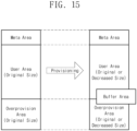
- FIG. 15 illustrates a diagram in which a buffer area is allocated in a reduction mode when the storage device 350 has an overprovision (OP) area.
- the storage device 350 may have an overprovision area in addition to a meta area and a user area.
- the overprovision area may be a storage space that is provided to improve the performance of the storage device 350. For example, in the case that free memory blocks in which data are not written exist, when a garbage collection operation or a read reclaim operation is performed on data written in the user area, the garbage collection operation and the read reclaim operation may be more quickly performed.
- the storage device 350 may provide the user area to the external host device, and may integrally leverage the user area and the overprovision area to write and manage user data.
- the storage device 350 may fixedly allocate a portion of the user area or the overprovision area for a buffer area.
- a portion of the buffer area may be included in the overprovision area, and a remainder of the buffer area may be included in the user area. Accordingly, the user area or the overprovision area may have an original size or a decreased size.
- FIG. 16 illustrates a diagram in which a buffer area is allocated in a non-reduction mode when the storage device 350 has an overprovision (OP) area.
- OP overprovision
- the storage device 350 may have an overprovision area in addition to a meta area and a user area.
- the storage device 350 may maintain original sizes of the user area or the overprovision area.
- the storage device 350 may dynamically allocate the user area or the overprovision area for a buffer area. A portion of the buffer area may be included in the overprovision area, and a remainder of the buffer area may be included in the user area.
- the processor 310 and the storage device 350 may perform the turbo write operation.
- the processor 310 may request the turbo write operation from the storage device 350.
- the request for the turbo write operation may use a write command UPIU based on the UFS.
- the write command UPIU may be identified as the request for the turbo write operation by setting a group number of the write command UPIU to a certain value, for example, "0x11."
- the storage device 350 may write data into the buffer area 112 in response to the write command UPIU having the group number of "0x11."
- the storage device 350 may transmit the response UPIU to the processor 310.
- the processor 310 and the storage device 350 may perform the normal write operation.
- the processor 310 may request the normal write operation from the storage device 350.
- the request for the normal write operation may use the write command UPIU based on the UFS.
- the storage device 350 may write data into the user area 111 in response to the write command UPIU.
- the storage device 350 may transmit the response UPIU to the processor 310.
- the processor 310 and the storage device 350 may perform a migration operation or may set the migration operation.
- the processor 310 may request the migration operation from the storage device 350.
- the request for the migration operation may be performed by using the query request UPIU based on the UFS.
- the processor 310 may transmit a set flag query request UPIU to the storage device 350.
- the set flag query request UPIU may include flush information or hibernation information.
- the storage device 350 may perform the migration operation, which is described with reference to FIG. 7 , in response to the set flag query request UPIU.
- the storage device 350 may change migration settings. For example, in response to the set flag query request UPIU, the storage device 350 may change the migration settings such that the migration operation is autonomously performed in the hibernation mode or such that the autonomous migration operation is not performed.
- the storage device 350 may transmit the response UPIU to the processor 310.
- the response UPIU may include the available buffer size. That is, when the migration operation is completed, the storage device 350 may identify the available buffer size and may report to the processor 310 on the available buffer size.
- the processor 310 and the storage device 350 may perform a buffer size query operation. For example, in operation S450, the processor 310 may query to the storage device 350 to obtain the buffer size. The query about the buffer size may be performed by using a query request based on the UFS.
- the processor 310 may transmit a read attributes query request UPIU to the storage device 350.
- the storage device 350 may transmit the response UPIU to the processor 310.
- the response UPIU may include the available buffer size.
- the storage device 350 may identify the available buffer size and may provide an indication of the available buffer size to the processor 310.
- the turbo write operation, the normal write operation, and the migration operation may be autonomously performed by the controller 220.
- the storage device 350 may perform the provisioning operation in response to a request of the processor 310.
- the buffer size query operation may be omitted.
- the processor 310 may determine whether the size of the data to be written is greater than the available buffer size. When the size of the data to be written is not greater than the available buffer size, in operation S530, the processor 310 may perform the turbo write operation of writing data into the buffer area 112.
- the processor 310 may divide the data into a turbo portion and a normal portion. In operation S550, the processor 310 may perform the turbo write operation of writing the turbo portion of the data into the buffer area 112.
- the processor 310 may perform the normal write operation of writing the normal portion of the data into the user area 111. That is, the processor 310 may split the data to be written and may write the split portions into the storage device 350 through the turbo write operation and the normal write operation.
- the processor 310 may perform the normal write operation of writing the data into the user area 111 of the storage device 350.
- the method described with reference to FIG. 17 may be autonomously performed by the controller 220.
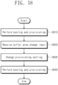
- FIG. 18 illustrates a method of the computing device 300 changing a size of a buffer area.
- the computing device 300 may perform booting when power is supplied and provisioning, as described above.
- the processor 310 may perform the provisioning operation with the storage device 350, based on the size of the buffer area of the existing provisioning settings.
- the computing device 300 may execute an operating system and applications under control of a user.
- the computing device 300 may receive a buffer area change input.
- the computing device 300 may receive the buffer area change input from the user through the user interface 340.
- the processor 310 may update the size of the buffer area of the provisioning settings.
- the computing device 300 may again perform booting and provisioning.
- the processor 310 may perform the provisioning operation with the storage device 350, based on the size of the buffer area of the updated provisioning settings.
- the computing device 300 may change the size of the buffer area, based on an input of the user. Changing the size of the buffer area may accompany rebooting and re-provisioning. As the change of the size of the buffer area is permitted, the computing device 300 may provide greater flexibility to the user.
- an existing memory block that has been used as the user area may be utilized as the buffer area.
- an existing memory block that has been utilized as the buffer area may be used as the user area.
- the storage device 350 may differently manage a certain memory block, based on whether the certain memory block is included in the buffer area. For example, the storage device 350 may manage parameters such as a read count and the number of program/erase cycles of a memory block and may manage data by using the parameters.
- the storage device 350 may differently set a weight to be applied to a read count and a weight to be applied to the number of program/erase cycles, based on whether a certain memory block is included in the buffer area. For example, a smaller (or greater) weight may be applied to a read count of a memory block belonging to the buffer area, and a smaller (or greater) weight may be applied to the number of program/erase cycles of the memory block belonging to the buffer area.
- components of the storage device 100 or 200 and the computing device 300 are described by using the terms “first,” “second,” “third,” and the like.
- first,” “second,” “third,” and the like may be used to distinguish components from each other and do not limit the descriptions thereof.
- first,” “second,” “third,” and the like do not involve an order or a numerical meaning of any form.
- the blocks and modules may be implemented with various hardware devices, such as an integrated circuit, an application certain IC (ASCI), a field programmable gate array (FPGA), and a complex programmable logic device (CPLD), firmware driven in hardware devices, software such as an application, or a combination of a hardware device and software.
- ASCI application certain IC
- FPGA field programmable gate array
- CPLD complex programmable logic device
- firmware driven in hardware devices software such as an application, or a combination of a hardware device and software.
- the blocks and modules may include circuits enrolled as circuits or semiconductor elements in an integrated circuit.
- an available buffer size of a buffer area is identified based on whether a reuse time elapses after a memory block of the buffer area is erased. Accordingly, a storage device and a computing device capable of preventing an error from occurring in the buffer area due to frequent erase operations and providing improved reliability are provided.
Landscapes
- Engineering & Computer Science (AREA)
- Theoretical Computer Science (AREA)
- Physics & Mathematics (AREA)
- General Engineering & Computer Science (AREA)
- General Physics & Mathematics (AREA)
- Human Computer Interaction (AREA)
- Computer Security & Cryptography (AREA)
- Techniques For Improving Reliability Of Storages (AREA)
Claims (13)
- Speicherungsvorrichtung (100), Folgendes umfassend:eine nichtflüchtige Speichervorrichtung (110) einschließlich einer Vielzahl von Speicherblöcken; undeine Steuerung (120), die konfiguriert ist, um einige Speicherblöcke der Vielzahl von Speicherblöcken als Pufferbereich (112) zu verwenden,wobei Speicherblöcke, die ungültige Daten unter den einigen Speicherblöcken speichern, ungültige Speicherblöcke (BLK17-20) sind, unddadurch gekennzeichnet, dass die Steuerung ferner zu Folgendem konfiguriert ist:Identifizieren von Speicherblöcken, bei denen eine verstrichene Zeit nach dem Löschen größer als eine Wiederverwendungszeit ist, unter den ungültigen Speicherblöcken, als verfügbare Speicherblöcke des Pufferbereichs; undBereitstellen einer verfügbaren Puffergröße für eine externe Hostvorrichtung, wobei die verfügbare Puffergröße eine Anzahl und/oder Kapazität der verfügbaren Speicherblöcke angibt,wobei die Wiederverwendungszeit eine vorbestimmte Zeit ist, in Bezug auf die die Verfügbarkeit oder Nichtverfügbarkeit des Speicherblocks auf der Grundlage einer Zeit beurteilt wird, im Laufe derer Ladungen entladen werden, die infolge einer Löschoperation in einer tunnelnden Isolierschicht oder einer blockierenden Isolierschicht einer Speicherzelle des Speicherblocks eingeschlossen sind, um die Schwellenspannung zu senken, bevor der Block verfügbar gemacht wird.
- Speicherungsvorrichtung (100) nach Anspruch 1, wobei die Steuerung (120) konfiguriert ist, um die ungültigen Speicherblöcke als Reaktion auf eine Anforderung der externen Hostvorrichtung oder periodisch zu überprüfen und die verfügbare Puffergröße basierend auf einem Ergebnis der Überprüfung zu aktualisieren.
- Speicherungsvorrichtung (100) nach Anspruch 1 oder 2, wobei die Steuerung (120) konfiguriert ist, um die verfügbare Puffergröße für die externe Hostvorrichtung bereitzustellen, als Reaktion auf eine Leseattributabfrageanforderung-UFS-Protokollinformationseinheit, UPIU, basierend auf einem universellen Flash-Speicher, UFS, die von der externen Hostvorrichtung empfangen wird.
- Speicherungsvorrichtung (100) nach einem der vorhergehenden Ansprüche, wobei die Steuerung (120) zu Folgendem konfiguriert ist:Empfangen eines Schreibbefehls, einer Adresse und Daten von der externen Hostvorrichtung;Schreiben der Daten in verfügbare Speicherblöcke des Pufferbereichs (112), wenn der Schreibbefehl ein Turbo-Schreibbefehl ist;Schreiben der Daten an einer Stelle, die die Adresse angibt, von anderen Speicherblöcken außer dem Pufferbereich, wenn der Schreibbefehl ein normaler Schreibbefehl ist.
- Speicherungsvorrichtung (100) nach Anspruch 4, wobei der Turbo-Schreibbefehl und der normale Schreibbefehl unterschiedliche Gruppennummern in einer Schreibbefehl-UPIU basierend auf einem UFS aufweisen.
- Speicherungsvorrichtung (100) nach Anspruch 4 oder 5, wobei der Turbo-Schreibbefehl Folgendes einschließt:eine auf einem UFS basierende Abfrageanforderungs-UPIU zum Setzen eines Flags, die eine Turbo-Schreiboperation aktiviert; undeine Schreibbefehl-UPIU, die auf dem UFS basiert.
- Speicherungsvorrichtung (100) nach einem der Ansprüche 4 bis 6, wobei die Steuerung (120) als Reaktion auf eine Anforderung der externen Hostvorrichtung oder in einem Ruhezustand ferner zu Folgendem konfiguriert ist:
Migrieren von gültigen Daten, die in den Pufferbereich (112) geschrieben werden, an die Stelle, die die Adresse angibt, der anderen Speicherblöcke mit Ausnahme des Pufferbereichs und Ungültigmachen der gültigen Daten. - Speicherungsvorrichtung (100) nach Anspruch 7, wobei die Anforderung der externen Hostvorrichtung eine auf einem UFS basierende Abfrageanforderungs-UPIU zum Setzen eines Flags einschießt.
- Speicherungsvorrichtung (100) nach Anspruch 7 oder 8, wobei das Überführen der gültigen Daten in den Ruhezustand durch eine auf einem UFS basierende Abfrageanforderungs-UPIU zum Setzen eines Flags aktiviert und deaktiviert wird.
- Speicherungsvorrichtung (100) nach einem der vorhergehenden Ansprüche, wobei die Steuerung ferner zu Folgendem konfiguriert ist:Bereitstellen einer Kapazität der Vielzahl von Speicherblöcken für die externe Hostvorrichtung während eines Boot-Operation;Empfangen eines Beschaffungsbefehls einschließlich Kapazitätsinformationen des Pufferbereichs (112) von der externen Hostvorrichtung; undAuswählen der einigen Speicherblöcken aus der Vielzahl von Speicherblöcken basierend auf den Kapazitätsinformationen, damit sie dem Pufferbereich zugewiesen werden.
- Speicherungsvorrichtung (100) nach Anspruch 10, wobei der Beschaffungsbefehl ferner Modusinformationen einschließt, und
wobei, wenn die Modusinformationen einen Reduktionsmodus angeben, die Steuerung (120) ferner konfiguriert ist, um eine Speicherkapazität von verbleibenden Speicherblöcken der Vielzahl von Speicherblöcken, die nicht zu den einigen Speicherblöcken des Pufferbereichs (112) gehören, für die externe Hostvorrichtung als Benutzerbereich bereitzustellen. - Speicherungsvorrichtung (100) nach Anspruch 11, wobei die Steuerung (120) die einigen Speicherblöcke, die im Pufferbereich (112) eingeschlossen sind, fest auswählt, Speicherzellen der einigen Speicherblöcke als Single Level Cell verwendet und Speicherzellen der übrigen Speicherblöcke als mindestens Triple Level Cells verwendet.
- Speicherungsvorrichtung (100) nach Anspruch 10, wobei der Beschaffungsbefehl ferner Modusinformationen einschließt, und
wobei, wenn die Modusinformationen einen Nicht-Reduktionsmodus angeben, die Steuerung (120) ferner konfiguriert ist, um eine Speicherkapazität der Vielzahl von Speicherblöcken für die externe Hostvorrichtung als Benutzerbereich bereitzustellen.
Applications Claiming Priority (1)
| Application Number | Priority Date | Filing Date | Title |
|---|---|---|---|
| KR1020190029435A KR102746577B1 (ko) | 2019-03-14 | 2019-03-14 | 스토리지 장치 및 스토리지 장치를 포함하는 컴퓨팅 장치 |
Publications (2)
| Publication Number | Publication Date |
|---|---|
| EP3709175A1 EP3709175A1 (de) | 2020-09-16 |
| EP3709175B1 true EP3709175B1 (de) | 2024-12-25 |
Family
ID=69157595
Family Applications (1)
| Application Number | Title | Priority Date | Filing Date |
|---|---|---|---|
| EP20150631.8A Active EP3709175B1 (de) | 2019-03-14 | 2020-01-07 | Speichervorrichtung und rechenvorrichtung mit der speichervorrichtung |
Country Status (4)
| Country | Link |
|---|---|
| US (1) | US11132143B2 (de) |
| EP (1) | EP3709175B1 (de) |
| KR (1) | KR102746577B1 (de) |
| CN (1) | CN111694511B (de) |
Families Citing this family (10)
| Publication number | Priority date | Publication date | Assignee | Title |
|---|---|---|---|---|
| US10901903B2 (en) * | 2018-12-21 | 2021-01-26 | Micron Technology, Inc. | Flash memory persistent cache techniques |
| JP7490469B2 (ja) * | 2020-06-25 | 2024-05-27 | キオクシア株式会社 | ストレージデバイス、ストレージシステム及び制御方法 |
| DE102022100592A1 (de) * | 2021-02-05 | 2022-08-11 | Samsung Electronics Co., Ltd. | Betriebsverfahren eines Universal-Flash-Storage-Hosts und Betriebsverfahren eines Universal-Flash-Storage-Systems |
| KR20220158372A (ko) | 2021-05-24 | 2022-12-01 | 에스케이하이닉스 주식회사 | 데이터 저장 장치 및 그 동작 방법 |
| US11481147B1 (en) * | 2021-06-17 | 2022-10-25 | EMC IP Holding Company LLC | Buffer allocation techniques |
| US11614896B2 (en) | 2021-08-06 | 2023-03-28 | Western Digital Technologies, Inc. | UFS out of order hint generation |
| US11829615B2 (en) | 2022-02-16 | 2023-11-28 | Western Digital Technologies, Inc. | Out of order data transfer hint calibration |
| US11853201B2 (en) * | 2022-05-25 | 2023-12-26 | Micron Technology, Inc. | Selective single-level memory cell operation |
| US12547336B2 (en) * | 2023-03-30 | 2026-02-10 | Silicon Motion, Inc. | Control method of memory device and associated flash memory controller |
| WO2024253745A1 (en) * | 2023-06-06 | 2024-12-12 | Qualcomm Incorporated | Universal flash storage shared write booster buffer enhancements |
Family Cites Families (21)
| Publication number | Priority date | Publication date | Assignee | Title |
|---|---|---|---|---|
| US4433374A (en) * | 1980-11-14 | 1984-02-21 | Sperry Corporation | Cache/disk subsystem with cache bypass |
| JP2008152464A (ja) | 2006-12-15 | 2008-07-03 | Toshiba Corp | 記憶装置 |
| JP4461170B2 (ja) | 2007-12-28 | 2010-05-12 | 株式会社東芝 | メモリシステム |
| US8060719B2 (en) | 2008-05-28 | 2011-11-15 | Micron Technology, Inc. | Hybrid memory management |
| KR101861170B1 (ko) | 2011-08-17 | 2018-05-25 | 삼성전자주식회사 | 마이그레이션 관리자를 포함하는 메모리 시스템 |
| KR20130060791A (ko) * | 2011-11-30 | 2013-06-10 | 삼성전자주식회사 | 마모도 제어 로직을 포함하는 메모리 시스템, 데이터 저장 장치, 메모리 카드, 그리고 솔리드 스테이트 드라이브 |
| KR20140033964A (ko) * | 2012-09-11 | 2014-03-19 | 삼성전자주식회사 | 단말기의 데이터 저장장치 및 방법 |
| KR102285462B1 (ko) * | 2014-03-26 | 2021-08-05 | 삼성전자주식회사 | 불휘발성 메모리 및 메모리 컨트롤러를 포함하는 메모리 시스템의 동작 방법 |
| US9959203B2 (en) * | 2014-06-23 | 2018-05-01 | Google Llc | Managing storage devices |
| US9841011B2 (en) | 2014-07-21 | 2017-12-12 | Lg Electronics Inc. | Linear compressor and a linear motor for a linear compressor |
| KR20160024530A (ko) | 2014-08-26 | 2016-03-07 | 에스케이하이닉스 주식회사 | 반도체 장치 및 이의 동작 방법 |
| US10430328B2 (en) * | 2014-09-16 | 2019-10-01 | Sandisk Technologies Llc | Non-volatile cache and non-volatile storage medium using single bit and multi bit flash memory cells or different programming parameters |
| KR102282962B1 (ko) | 2014-12-22 | 2021-07-30 | 삼성전자주식회사 | 스토리지 장치 및 스토리지 장치의 동작 방법 |
| KR102295223B1 (ko) * | 2015-01-13 | 2021-09-01 | 삼성전자주식회사 | 속도 모드 관리자를 포함하는 저장 장치 및 사용자 장치 |
| KR20170015708A (ko) | 2015-07-30 | 2017-02-09 | 삼성전자주식회사 | 불휘발성 메모리 장치를 포함하는 저장 장치 및 그것의 프로그램 방법 |
| KR20170044780A (ko) * | 2015-10-15 | 2017-04-26 | 에스케이하이닉스 주식회사 | 메모리 시스템 및 메모리 시스템의 동작방법 |
| KR102602694B1 (ko) * | 2015-12-15 | 2023-11-15 | 삼성전자주식회사 | 스토리지 컨트롤러의 작동 방법과 이를 포함하는 스토리지 장치의 작동 방법 |
| KR102601211B1 (ko) | 2016-06-01 | 2023-11-10 | 삼성전자주식회사 | 빠른 재사용 메모리 블록 검출 방법 및 이를 이용한 메모리 블록 관리 방법 |
| US10209900B2 (en) * | 2016-09-19 | 2019-02-19 | Fungible, Inc. | Buffer allocation and memory management using mapping table |
| US11133075B2 (en) * | 2017-07-07 | 2021-09-28 | Micron Technology, Inc. | Managed NAND power management |
| US10468077B2 (en) | 2018-02-07 | 2019-11-05 | Intel Corporation | Adaptive object buffering and meta-data indexing using persistent memory to improve flash memory durability in tiered storage |
-
2019
- 2019-03-14 KR KR1020190029435A patent/KR102746577B1/ko active Active
- 2019-09-20 US US16/577,790 patent/US11132143B2/en active Active
- 2019-12-27 CN CN201911376861.9A patent/CN111694511B/zh active Active
-
2020
- 2020-01-07 EP EP20150631.8A patent/EP3709175B1/de active Active
Also Published As
| Publication number | Publication date |
|---|---|
| US20200293221A1 (en) | 2020-09-17 |
| KR20200110547A (ko) | 2020-09-24 |
| CN111694511B (zh) | 2024-12-20 |
| US11132143B2 (en) | 2021-09-28 |
| KR102746577B1 (ko) | 2024-12-26 |
| EP3709175A1 (de) | 2020-09-16 |
| CN111694511A (zh) | 2020-09-22 |
Similar Documents
| Publication | Publication Date | Title |
|---|---|---|
| EP3709175A1 (de) | Speichervorrichtung und rechenvorrichtung mit der speichervorrichtung | |
| EP3872641B1 (de) | Speichervorrichtung und verfahren zum betrieb einer speichervorrichtung | |
| CN112306907B (zh) | 存储设备、包括其的存储系统及存储设备的操作方法 | |
| JP6517684B2 (ja) | メモリシステムおよび制御方法 | |
| JP6517685B2 (ja) | メモリシステムおよび制御方法 | |
| KR102098697B1 (ko) | 비휘발성 메모리 시스템, 이를 포함하는 시스템 및 상기 비휘발성 메모리 시스템의 적응적 사용자 저장 영역 조절 방법 | |
| US20240192883A1 (en) | Management of Storage Space in Solid State Drives to Support Proof of Space Activities | |
| KR101297563B1 (ko) | 스토리지 관리 방법 및 관리 시스템 | |
| US12086432B2 (en) | Gradually reclaim storage space occupied by a proof of space plot in a solid state drive | |
| US11392309B2 (en) | Memory system for performing migration operation and operating method thereof | |
| US12293106B2 (en) | Storage device, storage system, and control method | |
| KR20150133913A (ko) | 메모리 컨트롤러의 동작 방법 | |
| US11775188B2 (en) | Communications to reclaim storage space occupied by proof of space plots in solid state drives | |
| KR20150055413A (ko) | 데이터 저장 장치 | |
| KR20200114052A (ko) | 컨트롤러, 메모리 시스템 및 그것의 동작 방법 | |
| US20250217284A1 (en) | Garbage collection for flash translation layer tables | |
| US12314181B2 (en) | Data storage device with memory services for storage access queues | |
| US20240264750A1 (en) | Atomic Operations Implemented using Memory Services of Data Storage Devices | |
| US20250013570A1 (en) | Performance Optimization for Loading Data in Memory Services Configured on Storage Capacity of a Data Storage Device | |
| US20250013367A1 (en) | Performance Optimization for Storing Data in Memory Services Configured on Storage Capacity of a Data Storage Device | |
| US20240193085A1 (en) | Data Storage Device with Memory Services based on Storage Capacity | |
| US20250348424A1 (en) | Memory controller for ensuring write performance, storage apparatus having the same, and operation method thereof | |
| US20240143226A1 (en) | Data storage device and method for managing a write buffer | |
| WO2018051387A1 (ja) | 情報処理システムおよびデータ格納方法 | |
| KR20250066032A (ko) | 스토리지 장치 및 그것의 동작 방법 |
Legal Events
| Date | Code | Title | Description |
|---|---|---|---|
| PUAI | Public reference made under article 153(3) epc to a published international application that has entered the european phase |
Free format text: ORIGINAL CODE: 0009012 |
|
| STAA | Information on the status of an ep patent application or granted ep patent |
Free format text: STATUS: THE APPLICATION HAS BEEN PUBLISHED |
|
| AK | Designated contracting states |
Kind code of ref document: A1 Designated state(s): AL AT BE BG CH CY CZ DE DK EE ES FI FR GB GR HR HU IE IS IT LI LT LU LV MC MK MT NL NO PL PT RO RS SE SI SK SM TR |
|
| AX | Request for extension of the european patent |
Extension state: BA ME |
|
| STAA | Information on the status of an ep patent application or granted ep patent |
Free format text: STATUS: REQUEST FOR EXAMINATION WAS MADE |
|
| 17P | Request for examination filed |
Effective date: 20210224 |
|
| RBV | Designated contracting states (corrected) |
Designated state(s): AL AT BE BG CH CY CZ DE DK EE ES FI FR GB GR HR HU IE IS IT LI LT LU LV MC MK MT NL NO PL PT RO RS SE SI SK SM TR |
|
| STAA | Information on the status of an ep patent application or granted ep patent |
Free format text: STATUS: EXAMINATION IS IN PROGRESS |
|
| 17Q | First examination report despatched |
Effective date: 20220610 |
|
| P01 | Opt-out of the competence of the unified patent court (upc) registered |
Effective date: 20230520 |
|
| GRAP | Despatch of communication of intention to grant a patent |
Free format text: ORIGINAL CODE: EPIDOSNIGR1 |
|
| STAA | Information on the status of an ep patent application or granted ep patent |
Free format text: STATUS: GRANT OF PATENT IS INTENDED |
|
| INTG | Intention to grant announced |
Effective date: 20240718 |
|
| GRAS | Grant fee paid |
Free format text: ORIGINAL CODE: EPIDOSNIGR3 |
|
| GRAA | (expected) grant |
Free format text: ORIGINAL CODE: 0009210 |
|
| STAA | Information on the status of an ep patent application or granted ep patent |
Free format text: STATUS: THE PATENT HAS BEEN GRANTED |
|
| AK | Designated contracting states |
Kind code of ref document: B1 Designated state(s): AL AT BE BG CH CY CZ DE DK EE ES FI FR GB GR HR HU IE IS IT LI LT LU LV MC MK MT NL NO PL PT RO RS SE SI SK SM TR |
|
| REG | Reference to a national code |
Ref country code: GB Ref legal event code: FG4D |
|
| REG | Reference to a national code |
Ref country code: CH Ref legal event code: EP |
|
| REG | Reference to a national code |
Ref country code: DE Ref legal event code: R096 Ref document number: 602020043565 Country of ref document: DE |
|
| REG | Reference to a national code |
Ref country code: IE Ref legal event code: FG4D |
|
| REG | Reference to a national code |
Ref country code: NL Ref legal event code: FP |
|
| REG | Reference to a national code |
Ref country code: LT Ref legal event code: MG9D |
|
| PG25 | Lapsed in a contracting state [announced via postgrant information from national office to epo] |
Ref country code: HR Free format text: LAPSE BECAUSE OF FAILURE TO SUBMIT A TRANSLATION OF THE DESCRIPTION OR TO PAY THE FEE WITHIN THE PRESCRIBED TIME-LIMIT Effective date: 20241225 |
|
| PG25 | Lapsed in a contracting state [announced via postgrant information from national office to epo] |
Ref country code: FI Free format text: LAPSE BECAUSE OF FAILURE TO SUBMIT A TRANSLATION OF THE DESCRIPTION OR TO PAY THE FEE WITHIN THE PRESCRIBED TIME-LIMIT Effective date: 20241225 |
|
| PG25 | Lapsed in a contracting state [announced via postgrant information from national office to epo] |
Ref country code: BG Free format text: LAPSE BECAUSE OF FAILURE TO SUBMIT A TRANSLATION OF THE DESCRIPTION OR TO PAY THE FEE WITHIN THE PRESCRIBED TIME-LIMIT Effective date: 20241225 |
|
| PG25 | Lapsed in a contracting state [announced via postgrant information from national office to epo] |
Ref country code: NO Free format text: LAPSE BECAUSE OF FAILURE TO SUBMIT A TRANSLATION OF THE DESCRIPTION OR TO PAY THE FEE WITHIN THE PRESCRIBED TIME-LIMIT Effective date: 20250325 |
|
| PG25 | Lapsed in a contracting state [announced via postgrant information from national office to epo] |
Ref country code: LV Free format text: LAPSE BECAUSE OF FAILURE TO SUBMIT A TRANSLATION OF THE DESCRIPTION OR TO PAY THE FEE WITHIN THE PRESCRIBED TIME-LIMIT Effective date: 20241225 Ref country code: GR Free format text: LAPSE BECAUSE OF FAILURE TO SUBMIT A TRANSLATION OF THE DESCRIPTION OR TO PAY THE FEE WITHIN THE PRESCRIBED TIME-LIMIT Effective date: 20250326 |
|
| PG25 | Lapsed in a contracting state [announced via postgrant information from national office to epo] |
Ref country code: RS Free format text: LAPSE BECAUSE OF FAILURE TO SUBMIT A TRANSLATION OF THE DESCRIPTION OR TO PAY THE FEE WITHIN THE PRESCRIBED TIME-LIMIT Effective date: 20250325 |
|
| REG | Reference to a national code |
Ref country code: AT Ref legal event code: MK05 Ref document number: 1754764 Country of ref document: AT Kind code of ref document: T Effective date: 20241225 |
|
| PG25 | Lapsed in a contracting state [announced via postgrant information from national office to epo] |
Ref country code: SM Free format text: LAPSE BECAUSE OF FAILURE TO SUBMIT A TRANSLATION OF THE DESCRIPTION OR TO PAY THE FEE WITHIN THE PRESCRIBED TIME-LIMIT Effective date: 20241225 |
|
| PG25 | Lapsed in a contracting state [announced via postgrant information from national office to epo] |
Ref country code: PL Free format text: LAPSE BECAUSE OF FAILURE TO SUBMIT A TRANSLATION OF THE DESCRIPTION OR TO PAY THE FEE WITHIN THE PRESCRIBED TIME-LIMIT Effective date: 20241225 |
|
| PG25 | Lapsed in a contracting state [announced via postgrant information from national office to epo] |
Ref country code: ES Free format text: LAPSE BECAUSE OF FAILURE TO SUBMIT A TRANSLATION OF THE DESCRIPTION OR TO PAY THE FEE WITHIN THE PRESCRIBED TIME-LIMIT Effective date: 20241225 |
|
| PG25 | Lapsed in a contracting state [announced via postgrant information from national office to epo] |
Ref country code: IS Free format text: LAPSE BECAUSE OF FAILURE TO SUBMIT A TRANSLATION OF THE DESCRIPTION OR TO PAY THE FEE WITHIN THE PRESCRIBED TIME-LIMIT Effective date: 20250425 |
|
| PG25 | Lapsed in a contracting state [announced via postgrant information from national office to epo] |
Ref country code: PT Free format text: LAPSE BECAUSE OF FAILURE TO SUBMIT A TRANSLATION OF THE DESCRIPTION OR TO PAY THE FEE WITHIN THE PRESCRIBED TIME-LIMIT Effective date: 20250428 |
|
| PG25 | Lapsed in a contracting state [announced via postgrant information from national office to epo] |
Ref country code: EE Free format text: LAPSE BECAUSE OF FAILURE TO SUBMIT A TRANSLATION OF THE DESCRIPTION OR TO PAY THE FEE WITHIN THE PRESCRIBED TIME-LIMIT Effective date: 20241225 |
|
| PG25 | Lapsed in a contracting state [announced via postgrant information from national office to epo] |
Ref country code: AT Free format text: LAPSE BECAUSE OF FAILURE TO SUBMIT A TRANSLATION OF THE DESCRIPTION OR TO PAY THE FEE WITHIN THE PRESCRIBED TIME-LIMIT Effective date: 20241225 Ref country code: RO Free format text: LAPSE BECAUSE OF FAILURE TO SUBMIT A TRANSLATION OF THE DESCRIPTION OR TO PAY THE FEE WITHIN THE PRESCRIBED TIME-LIMIT Effective date: 20241225 |
|
| PG25 | Lapsed in a contracting state [announced via postgrant information from national office to epo] |
Ref country code: SK Free format text: LAPSE BECAUSE OF FAILURE TO SUBMIT A TRANSLATION OF THE DESCRIPTION OR TO PAY THE FEE WITHIN THE PRESCRIBED TIME-LIMIT Effective date: 20241225 |
|
| PG25 | Lapsed in a contracting state [announced via postgrant information from national office to epo] |
Ref country code: CZ Free format text: LAPSE BECAUSE OF FAILURE TO SUBMIT A TRANSLATION OF THE DESCRIPTION OR TO PAY THE FEE WITHIN THE PRESCRIBED TIME-LIMIT Effective date: 20241225 |
|
| PG25 | Lapsed in a contracting state [announced via postgrant information from national office to epo] |
Ref country code: IT Free format text: LAPSE BECAUSE OF FAILURE TO SUBMIT A TRANSLATION OF THE DESCRIPTION OR TO PAY THE FEE WITHIN THE PRESCRIBED TIME-LIMIT Effective date: 20241225 |
|
| REG | Reference to a national code |
Ref country code: CH Ref legal event code: PL |
|
| PG25 | Lapsed in a contracting state [announced via postgrant information from national office to epo] |
Ref country code: SE Free format text: LAPSE BECAUSE OF FAILURE TO SUBMIT A TRANSLATION OF THE DESCRIPTION OR TO PAY THE FEE WITHIN THE PRESCRIBED TIME-LIMIT Effective date: 20241225 |
|
| PG25 | Lapsed in a contracting state [announced via postgrant information from national office to epo] |
Ref country code: MC Free format text: LAPSE BECAUSE OF FAILURE TO SUBMIT A TRANSLATION OF THE DESCRIPTION OR TO PAY THE FEE WITHIN THE PRESCRIBED TIME-LIMIT Effective date: 20241225 Ref country code: LU Free format text: LAPSE BECAUSE OF NON-PAYMENT OF DUE FEES Effective date: 20250107 |
|
| REG | Reference to a national code |
Ref country code: DE Ref legal event code: R097 Ref document number: 602020043565 Country of ref document: DE |
|
| PG25 | Lapsed in a contracting state [announced via postgrant information from national office to epo] |
Ref country code: DK Free format text: LAPSE BECAUSE OF FAILURE TO SUBMIT A TRANSLATION OF THE DESCRIPTION OR TO PAY THE FEE WITHIN THE PRESCRIBED TIME-LIMIT Effective date: 20241225 |
|
| PG25 | Lapsed in a contracting state [announced via postgrant information from national office to epo] |
Ref country code: BE Free format text: LAPSE BECAUSE OF NON-PAYMENT OF DUE FEES Effective date: 20250131 |
|
| PG25 | Lapsed in a contracting state [announced via postgrant information from national office to epo] |
Ref country code: CH Free format text: LAPSE BECAUSE OF NON-PAYMENT OF DUE FEES Effective date: 20250131 |
|
| REG | Reference to a national code |
Ref country code: BE Ref legal event code: MM Effective date: 20250131 |
|
| PLBE | No opposition filed within time limit |
Free format text: ORIGINAL CODE: 0009261 |
|
| STAA | Information on the status of an ep patent application or granted ep patent |
Free format text: STATUS: NO OPPOSITION FILED WITHIN TIME LIMIT |
|
| 26N | No opposition filed |
Effective date: 20250926 |
|
| PGFP | Annual fee paid to national office [announced via postgrant information from national office to epo] |
Ref country code: NL Payment date: 20251126 Year of fee payment: 7 |
|
| PGFP | Annual fee paid to national office [announced via postgrant information from national office to epo] |
Ref country code: GB Payment date: 20251127 Year of fee payment: 7 |
|
| PG25 | Lapsed in a contracting state [announced via postgrant information from national office to epo] |
Ref country code: FR Free format text: LAPSE BECAUSE OF NON-PAYMENT OF DUE FEES Effective date: 20250225 |
|
| PG25 | Lapsed in a contracting state [announced via postgrant information from national office to epo] |
Ref country code: IE Free format text: LAPSE BECAUSE OF NON-PAYMENT OF DUE FEES Effective date: 20250107 |
|
| PGFP | Annual fee paid to national office [announced via postgrant information from national office to epo] |
Ref country code: DE Payment date: 20251126 Year of fee payment: 7 |